EP3163606A1 - Flash memory and fabricating method thereof - Google Patents
Flash memory and fabricating method thereof Download PDFInfo
- Publication number
- EP3163606A1 EP3163606A1 EP16194585.2A EP16194585A EP3163606A1 EP 3163606 A1 EP3163606 A1 EP 3163606A1 EP 16194585 A EP16194585 A EP 16194585A EP 3163606 A1 EP3163606 A1 EP 3163606A1
- Authority
- EP
- European Patent Office
- Prior art keywords
- gate
- dielectric layer
- transistors
- selecting
- transistor
- Prior art date
- Legal status (The legal status is an assumption and is not a legal conclusion. Google has not performed a legal analysis and makes no representation as to the accuracy of the status listed.)
- Withdrawn
Links
Images

Classifications
-
- H—ELECTRICITY
- H10—SEMICONDUCTOR DEVICES; ELECTRIC SOLID-STATE DEVICES NOT OTHERWISE PROVIDED FOR
- H10B—ELECTRONIC MEMORY DEVICES
- H10B41/00—Electrically erasable-and-programmable ROM [EEPROM] devices comprising floating gates
-
- H—ELECTRICITY
- H10—SEMICONDUCTOR DEVICES; ELECTRIC SOLID-STATE DEVICES NOT OTHERWISE PROVIDED FOR
- H10B—ELECTRONIC MEMORY DEVICES
- H10B41/00—Electrically erasable-and-programmable ROM [EEPROM] devices comprising floating gates
- H10B41/30—Electrically erasable-and-programmable ROM [EEPROM] devices comprising floating gates characterised by the memory core region
- H10B41/35—Electrically erasable-and-programmable ROM [EEPROM] devices comprising floating gates characterised by the memory core region with a cell select transistor, e.g. NAND
-
- H—ELECTRICITY
- H10—SEMICONDUCTOR DEVICES; ELECTRIC SOLID-STATE DEVICES NOT OTHERWISE PROVIDED FOR
- H10B—ELECTRONIC MEMORY DEVICES
- H10B41/00—Electrically erasable-and-programmable ROM [EEPROM] devices comprising floating gates
- H10B41/40—Electrically erasable-and-programmable ROM [EEPROM] devices comprising floating gates characterised by the peripheral circuit region
- H10B41/41—Electrically erasable-and-programmable ROM [EEPROM] devices comprising floating gates characterised by the peripheral circuit region of a memory region comprising a cell select transistor, e.g. NAND
-
- H—ELECTRICITY
- H10—SEMICONDUCTOR DEVICES; ELECTRIC SOLID-STATE DEVICES NOT OTHERWISE PROVIDED FOR
- H10B—ELECTRONIC MEMORY DEVICES
- H10B41/00—Electrically erasable-and-programmable ROM [EEPROM] devices comprising floating gates
- H10B41/40—Electrically erasable-and-programmable ROM [EEPROM] devices comprising floating gates characterised by the peripheral circuit region
- H10B41/42—Simultaneous manufacture of periphery and memory cells
- H10B41/43—Simultaneous manufacture of periphery and memory cells comprising only one type of peripheral transistor
-
- H—ELECTRICITY
- H10—SEMICONDUCTOR DEVICES; ELECTRIC SOLID-STATE DEVICES NOT OTHERWISE PROVIDED FOR
- H10B—ELECTRONIC MEMORY DEVICES
- H10B41/00—Electrically erasable-and-programmable ROM [EEPROM] devices comprising floating gates
- H10B41/40—Electrically erasable-and-programmable ROM [EEPROM] devices comprising floating gates characterised by the peripheral circuit region
- H10B41/42—Simultaneous manufacture of periphery and memory cells
- H10B41/43—Simultaneous manufacture of periphery and memory cells comprising only one type of peripheral transistor
- H10B41/46—Simultaneous manufacture of periphery and memory cells comprising only one type of peripheral transistor with an inter-gate dielectric layer also being used as part of the peripheral transistor
-
- H—ELECTRICITY
- H10—SEMICONDUCTOR DEVICES; ELECTRIC SOLID-STATE DEVICES NOT OTHERWISE PROVIDED FOR
- H10B—ELECTRONIC MEMORY DEVICES
- H10B99/00—Subject matter not provided for in other groups of this subclass
-
- H—ELECTRICITY
- H10—SEMICONDUCTOR DEVICES; ELECTRIC SOLID-STATE DEVICES NOT OTHERWISE PROVIDED FOR
- H10D—INORGANIC ELECTRIC SEMICONDUCTOR DEVICES
- H10D1/00—Resistors, capacitors or inductors
-
- H—ELECTRICITY
- H10—SEMICONDUCTOR DEVICES; ELECTRIC SOLID-STATE DEVICES NOT OTHERWISE PROVIDED FOR
- H10D—INORGANIC ELECTRIC SEMICONDUCTOR DEVICES
- H10D30/00—Field-effect transistors [FET]
- H10D30/60—Insulated-gate field-effect transistors [IGFET]
- H10D30/68—Floating-gate IGFETs
- H10D30/681—Floating-gate IGFETs having only two programming levels
- H10D30/683—Floating-gate IGFETs having only two programming levels programmed by tunnelling of carriers, e.g. Fowler-Nordheim tunnelling
-
- H—ELECTRICITY
- H10—SEMICONDUCTOR DEVICES; ELECTRIC SOLID-STATE DEVICES NOT OTHERWISE PROVIDED FOR
- H10D—INORGANIC ELECTRIC SEMICONDUCTOR DEVICES
- H10D62/00—Semiconductor bodies, or regions thereof, of devices having potential barriers
- H10D62/10—Shapes, relative sizes or dispositions of the regions of the semiconductor bodies; Shapes of the semiconductor bodies
- H10D62/113—Isolations within a component, i.e. internal isolations
- H10D62/115—Dielectric isolations, e.g. air gaps
-
- H—ELECTRICITY
- H10—SEMICONDUCTOR DEVICES; ELECTRIC SOLID-STATE DEVICES NOT OTHERWISE PROVIDED FOR
- H10D—INORGANIC ELECTRIC SEMICONDUCTOR DEVICES
- H10D84/00—Integrated devices formed in or on semiconductor substrates that comprise only semiconducting layers, e.g. on Si wafers or on GaAs-on-Si wafers
- H10D84/01—Manufacture or treatment
- H10D84/0123—Integrating together multiple components covered by H10D12/00 or H10D30/00, e.g. integrating multiple IGBTs
- H10D84/0126—Integrating together multiple components covered by H10D12/00 or H10D30/00, e.g. integrating multiple IGBTs the components including insulated gates, e.g. IGFETs
- H10D84/0151—Manufacturing their isolation regions
-
- H—ELECTRICITY
- H10—SEMICONDUCTOR DEVICES; ELECTRIC SOLID-STATE DEVICES NOT OTHERWISE PROVIDED FOR
- H10D—INORGANIC ELECTRIC SEMICONDUCTOR DEVICES
- H10D84/00—Integrated devices formed in or on semiconductor substrates that comprise only semiconducting layers, e.g. on Si wafers or on GaAs-on-Si wafers
- H10D84/01—Manufacture or treatment
- H10D84/02—Manufacture or treatment characterised by using material-based technologies
- H10D84/03—Manufacture or treatment characterised by using material-based technologies using Group IV technology, e.g. silicon technology or silicon-carbide [SiC] technology
- H10D84/038—Manufacture or treatment characterised by using material-based technologies using Group IV technology, e.g. silicon technology or silicon-carbide [SiC] technology using silicon technology, e.g. SiGe
-
- H—ELECTRICITY
- H10—SEMICONDUCTOR DEVICES; ELECTRIC SOLID-STATE DEVICES NOT OTHERWISE PROVIDED FOR
- H10P—GENERIC PROCESSES OR APPARATUS FOR THE MANUFACTURE OR TREATMENT OF DEVICES COVERED BY CLASS H10
- H10P14/00—Formation of materials, e.g. in the shape of layers or pillars
- H10P14/60—Formation of materials, e.g. in the shape of layers or pillars of insulating materials
- H10P14/63—Formation of materials, e.g. in the shape of layers or pillars of insulating materials characterised by the formation processes
- H10P14/6326—Deposition processes
- H10P14/6328—Deposition from the gas or vapour phase
- H10P14/6334—Deposition from the gas or vapour phase using decomposition or reaction of gaseous or vapour phase compounds, i.e. chemical vapour deposition
-
- H—ELECTRICITY
- H10—SEMICONDUCTOR DEVICES; ELECTRIC SOLID-STATE DEVICES NOT OTHERWISE PROVIDED FOR
- H10P—GENERIC PROCESSES OR APPARATUS FOR THE MANUFACTURE OR TREATMENT OF DEVICES COVERED BY CLASS H10
- H10P14/00—Formation of materials, e.g. in the shape of layers or pillars
- H10P14/60—Formation of materials, e.g. in the shape of layers or pillars of insulating materials
- H10P14/65—Formation of materials, e.g. in the shape of layers or pillars of insulating materials characterised by treatments performed before or after the formation of the materials
- H10P14/6516—Formation of materials, e.g. in the shape of layers or pillars of insulating materials characterised by treatments performed before or after the formation of the materials of treatments performed after formation of the materials
- H10P14/6529—Formation of materials, e.g. in the shape of layers or pillars of insulating materials characterised by treatments performed before or after the formation of the materials of treatments performed after formation of the materials by exposure to a gas or vapour
-
- H—ELECTRICITY
- H10—SEMICONDUCTOR DEVICES; ELECTRIC SOLID-STATE DEVICES NOT OTHERWISE PROVIDED FOR
- H10P—GENERIC PROCESSES OR APPARATUS FOR THE MANUFACTURE OR TREATMENT OF DEVICES COVERED BY CLASS H10
- H10P14/00—Formation of materials, e.g. in the shape of layers or pillars
- H10P14/60—Formation of materials, e.g. in the shape of layers or pillars of insulating materials
- H10P14/65—Formation of materials, e.g. in the shape of layers or pillars of insulating materials characterised by treatments performed before or after the formation of the materials
- H10P14/6516—Formation of materials, e.g. in the shape of layers or pillars of insulating materials characterised by treatments performed before or after the formation of the materials of treatments performed after formation of the materials
- H10P14/6534—Formation of materials, e.g. in the shape of layers or pillars of insulating materials characterised by treatments performed before or after the formation of the materials of treatments performed after formation of the materials by exposure to a liquid
-
- H—ELECTRICITY
- H10—SEMICONDUCTOR DEVICES; ELECTRIC SOLID-STATE DEVICES NOT OTHERWISE PROVIDED FOR
- H10P—GENERIC PROCESSES OR APPARATUS FOR THE MANUFACTURE OR TREATMENT OF DEVICES COVERED BY CLASS H10
- H10P14/00—Formation of materials, e.g. in the shape of layers or pillars
- H10P14/60—Formation of materials, e.g. in the shape of layers or pillars of insulating materials
- H10P14/65—Formation of materials, e.g. in the shape of layers or pillars of insulating materials characterised by treatments performed before or after the formation of the materials
- H10P14/6516—Formation of materials, e.g. in the shape of layers or pillars of insulating materials characterised by treatments performed before or after the formation of the materials of treatments performed after formation of the materials
- H10P14/6546—Formation of materials, e.g. in the shape of layers or pillars of insulating materials characterised by treatments performed before or after the formation of the materials of treatments performed after formation of the materials to change the surface groups of the insulating materials
-
- H—ELECTRICITY
- H10—SEMICONDUCTOR DEVICES; ELECTRIC SOLID-STATE DEVICES NOT OTHERWISE PROVIDED FOR
- H10P—GENERIC PROCESSES OR APPARATUS FOR THE MANUFACTURE OR TREATMENT OF DEVICES COVERED BY CLASS H10
- H10P14/00—Formation of materials, e.g. in the shape of layers or pillars
- H10P14/60—Formation of materials, e.g. in the shape of layers or pillars of insulating materials
- H10P14/66—Formation of materials, e.g. in the shape of layers or pillars of insulating materials characterised by the type of materials
- H10P14/668—Formation of materials, e.g. in the shape of layers or pillars of insulating materials characterised by the type of materials the materials being characterised by the deposition precursor materials
- H10P14/6681—Formation of materials, e.g. in the shape of layers or pillars of insulating materials characterised by the type of materials the materials being characterised by the deposition precursor materials the precursor containing a compound comprising Si
-
- H—ELECTRICITY
- H10—SEMICONDUCTOR DEVICES; ELECTRIC SOLID-STATE DEVICES NOT OTHERWISE PROVIDED FOR
- H10P—GENERIC PROCESSES OR APPARATUS FOR THE MANUFACTURE OR TREATMENT OF DEVICES COVERED BY CLASS H10
- H10P14/00—Formation of materials, e.g. in the shape of layers or pillars
- H10P14/60—Formation of materials, e.g. in the shape of layers or pillars of insulating materials
- H10P14/69—Inorganic materials
- H10P14/692—Inorganic materials composed of oxides, glassy oxides or oxide-based glasses
- H10P14/6921—Inorganic materials composed of oxides, glassy oxides or oxide-based glasses containing silicon
- H10P14/69215—Inorganic materials composed of oxides, glassy oxides or oxide-based glasses containing silicon the material being a silicon oxide, e.g. SiO2
-
- H—ELECTRICITY
- H10—SEMICONDUCTOR DEVICES; ELECTRIC SOLID-STATE DEVICES NOT OTHERWISE PROVIDED FOR
- H10P—GENERIC PROCESSES OR APPARATUS FOR THE MANUFACTURE OR TREATMENT OF DEVICES COVERED BY CLASS H10
- H10P50/00—Etching of wafers, substrates or parts of devices
- H10P50/20—Dry etching; Plasma etching; Reactive-ion etching
- H10P50/28—Dry etching; Plasma etching; Reactive-ion etching of insulating materials
- H10P50/282—Dry etching; Plasma etching; Reactive-ion etching of insulating materials of inorganic materials
- H10P50/283—Dry etching; Plasma etching; Reactive-ion etching of insulating materials of inorganic materials by chemical means
-
- H—ELECTRICITY
- H10—SEMICONDUCTOR DEVICES; ELECTRIC SOLID-STATE DEVICES NOT OTHERWISE PROVIDED FOR
- H10W—GENERIC PACKAGES, INTERCONNECTIONS, CONNECTORS OR OTHER CONSTRUCTIONAL DETAILS OF DEVICES COVERED BY CLASS H10
- H10W10/00—Isolation regions in semiconductor bodies between components of integrated devices
- H10W10/01—Manufacture or treatment
- H10W10/021—Manufacture or treatment of air gaps
-
- H—ELECTRICITY
- H10—SEMICONDUCTOR DEVICES; ELECTRIC SOLID-STATE DEVICES NOT OTHERWISE PROVIDED FOR
- H10W—GENERIC PACKAGES, INTERCONNECTIONS, CONNECTORS OR OTHER CONSTRUCTIONAL DETAILS OF DEVICES COVERED BY CLASS H10
- H10W10/00—Isolation regions in semiconductor bodies between components of integrated devices
- H10W10/20—Air gaps
-
- H—ELECTRICITY
- H10—SEMICONDUCTOR DEVICES; ELECTRIC SOLID-STATE DEVICES NOT OTHERWISE PROVIDED FOR
- H10W—GENERIC PACKAGES, INTERCONNECTIONS, CONNECTORS OR OTHER CONSTRUCTIONAL DETAILS OF DEVICES COVERED BY CLASS H10
- H10W20/00—Interconnections in chips, wafers or substrates
- H10W20/01—Manufacture or treatment
- H10W20/071—Manufacture or treatment of dielectric parts thereof
- H10W20/072—Manufacture or treatment of dielectric parts thereof of dielectric parts comprising air gaps
-
- H—ELECTRICITY
- H10—SEMICONDUCTOR DEVICES; ELECTRIC SOLID-STATE DEVICES NOT OTHERWISE PROVIDED FOR
- H10W—GENERIC PACKAGES, INTERCONNECTIONS, CONNECTORS OR OTHER CONSTRUCTIONAL DETAILS OF DEVICES COVERED BY CLASS H10
- H10W20/00—Interconnections in chips, wafers or substrates
- H10W20/40—Interconnections external to wafers or substrates, e.g. back-end-of-line [BEOL] metallisations or vias connecting to gate electrodes
- H10W20/45—Interconnections external to wafers or substrates, e.g. back-end-of-line [BEOL] metallisations or vias connecting to gate electrodes characterised by their insulating parts
- H10W20/46—Interconnections external to wafers or substrates, e.g. back-end-of-line [BEOL] metallisations or vias connecting to gate electrodes characterised by their insulating parts comprising air gaps
Definitions
- the present invention generally relates to the field of semiconductor technologies and, more particularly, relates to a flash memory and a method for fabricating the flash memory.
- flash memory is one important type of the digital circuits.
- flash memory is particularly rapidly developed in memory device filed.
- a main feature of the flash memory is that the storage information can be maintained for a long term in an unpowered condition. So flash memories are widely used in rewritable data storages that require a variety of data to be stored without a power supply. Further, flash memory has many other advantages, such as high integration, fast access speed, being apt to erase and rewrite, etc. Therefore, flash memories are also widely used in many areas such as micro-electromechanical systems, automated control systems, etc.
- Flash memories are commonly used as the memory devices in such portable electronic devices, including digital cameras, laptops, tablet computers, smart phones, etc. Therefore, reducing the size of the flash memory cells and simultaneously reducing the cost of flash memory become one research direction of the technological development.
- the pitch between adjacent memory cells becomes smaller. Therefore, the adjacent memory cells may be interfered with each other when reading, writing or erasing operations are performed. Such interferences may result in an unreliable performance of the flash memory.
- a flash memory fabricating method is provided.
- a first aspect of the present invention provides a method for fabricating a flash memory, comprising: proving a substrate including a memory cell region; forming a memory transistor array including a plurality of memory transistors, and a plurality of selecting transistors in the memory cell region, wherein each selecting transistor is used for selecting one column of memory transistors in the memory transistor array; forming a functional layer covering outer surfaces of the plurality of memory transistors and selecting transistors, as well as surfaces of the substrate between adjacent memory transistors and selecting transistors; performing a surface roughening treatment to the functional layer to provide a roughed surface of the functional layer that absorbs water; making the roughed surface of the functional layer to absorb water; and forming a dielectric layer using a chemical vapor deposition process on the functional layer, wherein the absorbed water is evaporated from the roughed surface of the functional layer during the chemical vapor deposition process to form an upward air flow that resists the deposition of the dielectric layer, such that air gaps are formed between adjacent memory transistors, and the dielectric layer covers
- the memory transistor array may include a plurality of discrete gate stack structures of the plurality of memory transistors, and a plurality of source regions and drain regions on both sides of the gate stack structures; and each selecting transistor includes a gate structure, a source region and a drain region on both sides of the gate structure; wherein a first gap distance between adjacent gate stack structures of the plurality of memory transistors may be made smaller than a second gap distance between one gate structure of the selecting transistor and corresponding adjacent gate stack structure of one memory transistor.
- the method may further comprise: forming a plurality of logic transistors in a peripheral circuit region of the substrate; and each logic transistor includes a gate structure, a source region and a drain region on both sides of the gate structure; wherein the first gap distance between adjacent gate stack structures of the plurality of memory transistors is smaller than a third gap distance between one gate structure of the selecting transistor and corresponding adjacent gate structure of one logic transistor, and is also smaller than a fourth gap distance between adjacent gate structures of the plurality of logic transistors; and wherein the dielectric layer further covers the top surfaces of the plurality of logic transistors and selecting transistors and fills gaps between each selecting transistor and corresponding adjacent logic transistor, and gaps between adjacent logic transistors.
- Making the roughed surface of the functional layer to absorb water may be realized by performing a rinse treatment to the functional layer by using deionized water.
- Making the roughed surface of the functional layer to absorb water may be realized by placing the functional layer in an aqueous environment for 1 day to 10 days.
- a material of the functional layer may be silicon oxide; a thickness of the functional layer may be in a range from 20 ⁇ to 100 ⁇ ; the functional layer may be formed by using an atomic layer deposition method; and the surface roughening treatment to the functional layer may be a dry etching process.
- An etching gas of the dry etching process may be NF 3 ; a gas flow rate of the dry etching process is in a range from 10mL/min to 50mL/min; a power of the dry etching process may be in a range from 100W to 500W; and an etching time of the dry etching process may be in a range from 5s to 10s.
- the method may further comprise: using silicon oxide as a material of the dielectric layer; the chemical vapor deposition process using tetraethyl orthosilicate or silane to form the dielectric layer; and a temperature of the chemical vapor deposition process being in a range from 400 °C to 600 °C.
- the gate stack structure of each memory transistor may include a tunneling dielectric layer, a floating gate, an inner gate dielectric layer, and a control gate; a material of the tunneling dielectric layer may be silicon oxide; a material of the floating gate may be doped polysilicon; the inter gates dielectric layer may be a three-layer structure including silicon oxide, silicon nitride, and nitrogen oxide; and a material of the control gate may be doped polysilicon.
- each selecting transistor from bottom to top, may include a gate dielectric layer, a bottom gate electrode, an inner dummy gate dielectric layer, and a selecting gate; the inner dummy gate dielectric layer may have an opening, the bottom gate electrode and the selecting gate may be electrically connected through the opening; a material of the gate dielectric layer may be silicon oxide; a material of the bottom gate may be doped polysilicon; the inter dummy gate dielectric layer may be a three-layer structure including silicon oxide, silicon nitride, and nitrogen oxide; and a material of the selecting gate is doped polysilicon.
- the gate structure of each logic transistor may include a gate dielectric layer, a bottom gate electrode, an inner dummy gate dielectric layer, and a logic gate; the inner dummy gate dielectric layer has an opening, the bottom gate electrode and the logic gate may be electrically connected through the opening; a material of the gate dielectric layer may be silicon oxide; a material of the bottom gate may be doped polysilicon; the inter dummy gate dielectric layer may be a three-layer structure including silicon oxide, silicon nitride, and silicon oxide; and a material of the logic gate may be doped polysilicon.
- a metal silicide layer may be formed on top of the gate stack structure of each memory transistor, the gate structure of each selecting transistor, and the gate structure of each logic transistor; and the control gate, the selecting gate, and the logic gate may be word lines.
- the memory transistors and the selecting transistor in the memory cell region, as well as the logic transistors in the peripheral circuit region may be formed simultaneously following same fabricating processes.
- a flash memory comprising: a substrate including a memory cell region; a memory transistor array including a plurality of memory transistors, and a plurality of selecting transistors in the memory cell region, wherein each selecting transistor is used for selecting one column of memory transistors in the memory transistor array; a functional layer covering outer surfaces of the plurality of memory transistors and selecting transistors, as well as surfaces of the substrate between adjacent memory transistors and selecting transistors, wherein the functional layer has a roughed surface that absorbs water; a dielectric layer covers the top surfaces of the plurality of memory transistors and selecting transistors and fills gaps between each selecting transistor and corresponding adjacent memory transistor; and air gaps between adjacent memory transistors; wherein the dielectric layer is formed by using a chemical vapor deposition process, and the air gaps are formed by evaporating absorbed water from the roughed surface of the functional layer during the chemical vapor deposition process to form an upward air flow that resists the deposition of the dielectric layer.
- the memory transistor array may include a plurality of discrete gate stack structures of the plurality of memory transistors, and a plurality of source regions and drain regions on both sides of the gate stack structures; and each selecting transistor may include a gate structure, a source region and a drain region on both sides of the gate structure.
- a first gap distance between adjacent gate stack structures of the plurality of memory transistors may be smaller than a second gap distance between one gate structure of the selecting transistor and corresponding adjacent gate stack structure of one memory transistor.
- the flash memory may further comprises: a plurality of logic transistors in a peripheral circuit region of the substrate; and each logic transistor may include a gate structure, a source region and a drain region on both sides of the gate structure; wherein the first gap distance between adjacent gate stack structures of the plurality of memory transistors may be smaller than a third gap distance between one gate structure of the selecting transistor and corresponding adjacent gate structure of one logic transistor, and may be also smaller than a fourth gap distance between adjacent gate structures of the plurality of logic transistors; and wherein the dielectric layer further may cover the top surfaces of the plurality of logic transistors and selecting transistors and may fill gaps between each selecting transistor and corresponding adjacent logic transistor, and gaps between adjacent logic transistors.
- a material of the functional layer may be silicon oxide; a thickness of the functional layer may be in a range from 20 ⁇ to 100 ⁇ ; and a material of the dielectric layer may be silicon oxide.
- the gate stack structure of each memory transistor, from bottom to top, may include a tunneling dielectric layer, a floating gate, an inner gate dielectric layer, and a control gate, a material of the tunneling dielectric layer may be silicon oxide, a material of the floating gate may be doped polysilicon, the inter gates dielectric layer may be a three-layer structure including silicon oxide, silicon nitride, and nitrogen oxide, a material of the control gate may be doped polysilicon; the gate structure each selecting transistor, from bottom to top, may include a gate dielectric layer, a bottom gate electrode, an inner dummy gate dielectric layer, and a selecting gate, the inner dummy gate dielectric layer may have an opening, the bottom gate electrode and the selecting gate are electrically connected through the opening, a material of the gate dielectric layer may be silicon oxide, a material of the bottom gate is doped polysilicon, the inter dummy gate dielectric layer may be a three-layer structure including silicon oxide, silicon nitride, and nitrogen oxide, a material of the
- a metal silicide layer may be formed on top of the gate stack structure of each memory transistor, the gate structure of each selecting transistor, and the gate structure of each logic transistor.
- the pitch between adjacent memory cells becomes smaller. Therefore, the adjacent memory cells may be interfered from each other when reading, writing or erasing operations are performed. Such interferences may result in an unreliable performance of the flash memory.
- a dielectric layer is filled between adjacent flash memory cells to electrically insulate the gate stack structures of the adjacent flash memory cells.
- a material of the dielectric layer is generally silicon oxide, which may result in a too large parasitic capacitance during the charging and discharging process of the reading, writing, or erasing operations. Thus, a memory cell that is not supposed to be operated may be interfered to change the storage state by an adjacent memory cell that is operated.
- the present invention provides a flash memory and a fabricating method thereof.
- a high temperature of the depositing process can be used for evaporating the water absorbed in the functional layer to form water vapor.
- the evaporated water vapor can move upward to form a flow to resist the deposition of the dielectric layer. Therefore, the filling process for forming the dielectric layer can generate multiple air gaps between the gate stack structures of adjacent flash memory cells during the dielectric layer depositing process. As such, the parasitic capacitance can be reduced to avoid interference between adjacent flash memory cells.
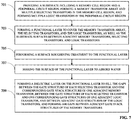
- FIG. 7 illustrates a flow chart of an exemplary process for fabricating a flash memory in accordance with some embodiments of the present invention
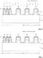
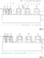
- FIGS. 1-6 illustrate cross sectional structures of an exemplary flash memory corresponding to certain stages of the exemplary fabricating process.
- a substrate including a memory cell region and a peripheral circuit region can be provided.
- a memory transistor array and multiple selecting transistors can be formed in the memory cell region, and multiple logic transistors can be formed in the peripheral circuit region.
- a substrate 10 can be provided.
- the substrate 10 includes a memory cell region I and the peripheral circuit region II.
- the memory cell region can include a memory transistor array, and multiple selecting transistors 102. Each selecting transistor can be used for selecting one row or one column of the memory transistors in the memory transistor array.
- the peripheral circuit region II can include multiple logic transistors.
- the memory transistor array includes multiple discrete gate stack structures 101 and source and drain regions (not shown in the figures) located on both sides of the gate stack structures 101.
- Each selecting transistor 102 includes a gate structure 102 and source and drain regions (not shown in the figure) located on both sides of the gate structure 102.
- the logic transistor includes a gate structure 103 and source and drain regions (not shown in the figure) located on both sides of the gate structure 103.
- the substrate 10 can be any suitable semiconductor substrate, such as a silicon substrate, a silicon on insulator (SOI) substrate, etc.
- the gate stack structures 101 of the memory transistors in the memory cell region I have a relatively small density, so that adjacent gate stack structures 101 has a relatively small gap.
- the gaps between the gate structure 102 of each selecting transistor and corresponding gate stack structure 101 of one adjacent memory transistors, the gaps between the gate structure of each selecting transistor and corresponding gate structure 103 of one adjacent logic transistor, and the gaps between adjacent gate structures 103 of the logic transistors, are relatively large.
- the gate stack structure 101 of each memory transistor can include a tunneling dielectric layer 101a, a floating gate 101b, an inner gate dielectric layer 101c, and a control gate 101d.
- a material of the tunneling dielectric layer 101a is silicon oxide
- a material of the floating gate 101b is doped polysilicon.
- the inter gates dielectric layer 101c is a three-layer structure including silicon oxide, silicon nitride, and nitrogen oxide (ONO).
- a material of the control gate 101d is also doped polysilicon.
- the gate structure 102 of each selecting transistor can include a gate dielectric layer 102a, a bottom gate electrode 102b, an inner dummy gate dielectric layer 102c, and a selecting gate 102d.
- the inner dummy gate dielectric layer 102c has an opening, the bottom gate electrode 102b and the selecting gate 102d are electrically connected through the opening.
- a material of the gate dielectric layer 102a is silicon oxide
- a material of the bottom gate 102b is doped polysilicon.
- the inter dummy gate dielectric layer 102c is a three-layer structure including silicon oxide, silicon nitride, and nitrogen oxide (ONO).
- a material of the selecting gate 102d is also doped polysilicon.
- the gate structure 103 of each logic transistor can include a gate dielectric layer 103a, a bottom gate electrode 103b, an inner dummy gate dielectric layer 103c, and a logic gate 103d.
- the inner dummy gate dielectric layer 103c has an opening, the bottom gate electrode 103b and the logic gate 103d are electrically connected through the opening.
- a material of the gate dielectric layer 103a is silicon oxide
- a material of the bottom gate 103b is doped polysilicon.
- the inter dummy gate dielectric layer 103c is a three-layer structure including silicon oxide, silicon nitride, and silicon oxide (ONO).
- a material of the logic gate 103d is also doped polysilicon.
- the gate stack structures 101, and the gate structures 102, 103 can be made by the following steps.
- the tunneling dielectric layer 101a, and the gate dielectric layers 102a, 103a can be formed in a same layer by a same process.
- a silicon oxide layer can be thermally oxidized or deposited on the semiconductor substrate.
- a thickness difference between the tunneling dielectric layer 101a and the gate dielectric layer 102a or 103a can be predetermined.
- a patterned photoresist layer can be formed to cover a predetermined region in the memory cell region I that is to be formed as the selecting transistors, and to cover the silicon oxide in the peripheral circuit region II.
- the silicon oxide in the memory transistor region can be dry etched to expose the surface of the semiconductor substrate.
- the remaining photoresist layer can be ashed and removed.
- an additional silicon oxide layer can be deposited on the remaining silicon oxide and the exposed surface of the semiconductor substrate.
- a thickness of the additional silicon oxide layer can meet the requirement of the tunneling dielectric layer 101 a.
- a first silicon oxide layer having a first thickness can be formed in the predetermined regions of memory cell region I that are used to be formed as memory transistors.
- a second silicon oxide layer having a second thickness can be formed in the predetermined region of memory cell region I that is used to be formed as the selecting transistors, and in the peripheral circuit region II.
- a first doped polysilicon layer can be deposited on the first silicon oxide layer and the second silicon oxide layer.
- a three-layer structure including silicon oxide, silicon nitride, and silicon oxide (ONO) can be deposited sequentially from bottom to top on the first doped polysilicon layer.
- Multiple openings can then be dry etched in the ONO three-layer structure to expose the first doped polysilicon layer. The positions of the multiple openings can be located in the predetermined regions that are used to be formed as the gate structures of the selecting transistors and the logic transistors. Then a second doped polysilicon layer can be formed in the multiple openings.
- a hard mask layer can be deposited on the second doped polysilicon layer.
- a material of the hard mask layer can be silicon oxide.
- the hard mask layer cam be patterned. Using the patterned hard mask layer as a mask, the formed multi-layer structure including the second layer of doped polysilicon, the ONO three-layer structure, the first doped polysilicon layer and the silicon oxide can be dry etched to form discrete multiple gate stack structures 101 of the memory transistors, the gate structures 102 of the selecting transistors, and the gate structures 103 of the logic transistors.
- the second doped polysilicon layer can also be etched to form word lines.
- iron implantation processes can be performed respectively to the memory cell region I and the peripheral circuit region II of the semiconductor substrate to form corresponding source and drain regions (not shown in the figures) of the memory transistors, the selecting transistors, and the logic transistors.
- the ion implantation processes can include a shallow depth ion implantation process and a deep depth ion implantation process.
- the shallow ion implantation process can be performed by using the gate stack structures 101 of the memory transistors, the gate structure 102 of the selection transistor, and the gate structures 103 of the logic transistors as masks.
- side walls (not shown in the figures) can be formed on both sides of the gate stack structures 101 of the memory transistors, the gate structure 102 of the selection transistor, and the gate structures 103 of the logic transistors respectively.
- the deep ion implantation process can be performed by using the side walls as masks.
- buffer oxide layer 11 may be formed on the surface of the semiconductor substrate surface.
- a material of the buffer oxide layer 11, for example, can be silicon oxide.
- the buffer oxide layer 11 can be used to protect the surface of the semiconductor substrate during the shallow depth ion implantation process and the deep depth ion implantation process.
- metal silicide 12 can then be formed on the top portions of the gate stack structures 101 of the memory transistors, the gate structures 102 of the selecting transistors, and the gate structure 103 of the logic transistor 103.
- a pickling process can be firstly performed to remove the oxidized surface of the doped polysilicon.
- the pickling process can remove upper portions of the side walls to expose the upper portions of the gate stack structures 101 of the memory transistors, the gate structures 102 of the selecting transistors, and the gate structure 103 of the logic transistor 103.
- a metal material can be deposited on the exposed sidewalls of the upper portions of the gate stack structures 101 of the memory transistors, the gate structures 102 of the selecting transistors, and the gate structure 103 of the logic transistor 103, as well as the remaining lower portions of the side walls, and the buffer oxide layer 11.
- the metal material can be nickel. In some other embodiments, the metal material may be cobalt, titanium, or tungsten. After a high temperature silicifying process, the metal material can form the metal silicide 12. At last, the remaining metal that is not silicified can be removed by washing.
- the gate stack structures 101 of the memory transistors have relatively small widths, the exposed upper portions of the gate stack structures 101 of the memory transistors can be fully converted into metal silicide 12.
- the gate structures 102 of the selecting transistors and the gate structures 103 of the logic transistors have relatively large widths, certain thickness surfaces of the exposed upper portions of the gate structures 102 of the selecting transistors and the gate structures 103 of the logic transistors may be converted into metal silicide 12.
- a functional layer can be formed to cover the memory transistor array, the selecting transistors, and the logic transistors, as well as the substrate surfaces between adjacent memory transistors, selecting transistors, and logic transistors.
- a functional layer 13 can be formed by using an atomic layer deposition (ALD) method on the outer surfaces of the gate stack structures 101 of the memory transistor array, the gate structures 102 of the selecting transistors and the gate structures 103 of the logic transistors, and the exposed surfaces of the semiconductor substrate that are between adjacent gate stack structures 101, and/or gate structures 102, 103.
- ALD atomic layer deposition
- the buffer oxide layer 11 is covering the exposed surfaces of the semiconductor substrate that are between adjacent gate stack structures 101, and/or gate structures 102, 103.
- the functional layer 13 is formed on the buffer oxide layer 11.
- the functional layer 13 can be directly formed on the exposed surfaces of the semiconductor substrate that are between adjacent gate stack structures 101, and/or gate structures 102, 103.
- a material of the functional layer 13 may be silicon oxide, and a thickness of the functional layer 13 may be in a range from 20 ⁇ to 100 ⁇ .
- the reason that the functional layer 13 is formed by using the atomic layer deposition (ALD) method has two aspects. On one aspect, the functional layer 13 formed on the surfaces of the semiconductor substrate between adjacent gate stack structures 101 of the memory transistor array having relatively small gaps can have a uniform thickness. On the other aspect, the formed functional layer 13 can be relatively thin, and may fully fill the gaps between adjacent gate stack structures 101 of the memory transistor array.
- a surface roughening treatment can be performed in the functional layer.
- the functional layer 13 can be surface roughened to form a rough surface that can easily absorb water.
- the surface roughening treatment can be achieved by using a dry etching process.
- the dry etching gas can be NF 3
- the gas flow rate can be in a range from 10mL/min to 50mL/min
- the power can be in a range from 100W to 500W
- an etching time can be in a range from 5s to 10s.
- the surface of the functional layer can absorb water.
- the rough surface of the functional layer 13 can absorb water.
- the step can be realized by performing a rinse treatment to the functional layer 13 by using deionized water.
- the step can be realized by placing the functional layer 13 in an aqueous environment for 1 day to 10 days.
- the aqueous environment can be a clean room, and the functional layer 13 can absorb the atmospheric moisture.
- a dielectric layer can be formed on the functional layer.
- the dielectric layer can fill the gaps between the gate structure 102 of each selecting transistor and one corresponding gate stack structure 101 of one adjacent memory transistor, between the gate structure 102 of each selecting transistor and one corresponding gate structures 103 of one adjacent logic transistor, and between adjacent gate structures 103 of the logic transistors.
- air gaps can be formed between adjacent gate stack structures 101 of the memory transistors.
- a dielectric layer 14 can be formed on the water-absorbed functional layer 13 by using a chemical vapor deposition (CVD) process.
- the chemical vapor deposition can use tetraethyl orthosilicate (TEOS) or silane to form a silicon oxide dielectric layer 14.
- TEOS tetraethyl orthosilicate
- a deposition process temperature can be in a range from 400 °C to 600 °C.
- the deposition process temperature can evaporate the absorbed water by the functional layer 13 to form an upward air flow.
- the upward air flow can prevent the deposition of the dielectric layer 14, thereby providing a poor performance of the filling process of the dielectric layer 14.
- the gaps between the gate structure 102 of each selecting transistor and one corresponding gate stack structure 101 of one adjacent memory transistor, between the gate structure 102 of each selecting transistor and one corresponding gate structure 103 of one adjacent logic transistor, and between adjacent gate structures 103 of the logic transistors are relatively large. Therefore, even the filling process of the dielectric layer 14 has a poor performance, the dielectric layer 14 can fill the above described gaps.
- the gaps between adjacent gate stack structures 101 of the memory transistors are relatively small.
- the dielectric layer 14 can only cover the top portions of the gate stack structures 101 of the memory transistors. Therefore, air gaps can be formed between adjacent gate stack structures 101 of the memory transistors.
- the formed dielectric layer 14 can cover the top surfaces of the gate stack structures 101 of the memory transistors, the gate structures 102 of the selecting transistors, and the gate structures 103 of the logic transistor. Further, the formed dielectric layer 14 can fill the gaps between the gate structure 102 of each selecting transistor and one corresponding gate stack structure 101 of one adjacent memory transistor, between the gate structure 102 of each selecting transistor and one corresponding gate structure 103 of one adjacent logic transistor, and between adjacent gate structures 103 of the logic transistors. In the meantime, air gaps can be formed between adjacent gate stack structures 101 of the memory transistors.
- the memory transistors and the selecting transistors in the memory cell region I, as well as the logic transistors in the peripheral circuit region II are formed simultaneously following the same fabricating processes.
- the memory transistors and the selecting transistors in the memory cell region I, and the logic transistors in the peripheral circuit region II can be respectively formed by different fabricating processes.
Landscapes
- Engineering & Computer Science (AREA)
- Manufacturing & Machinery (AREA)
- Semiconductor Memories (AREA)
- Non-Volatile Memory (AREA)
- Chemical & Material Sciences (AREA)
- Chemical Kinetics & Catalysis (AREA)
- Power Engineering (AREA)
Abstract
Description
- This application claims the priority of Chinese patent application No.
201510714032.2, filed on October 28, 2015 - The present invention generally relates to the field of semiconductor technologies and, more particularly, relates to a flash memory and a method for fabricating the flash memory.
- In the current semiconductor industry, integrated circuit products can be divided into three categories: analog circuits, digital circuits, and digital/analog hybrid circuits. Memory device is one important type of the digital circuits. In recent years, flash memory is particularly rapidly developed in memory device filed. A main feature of the flash memory is that the storage information can be maintained for a long term in an unpowered condition. So flash memories are widely used in rewritable data storages that require a variety of data to be stored without a power supply. Further, flash memory has many other advantages, such as high integration, fast access speed, being apt to erase and rewrite, etc. Therefore, flash memories are also widely used in many areas such as micro-electromechanical systems, automated control systems, etc.
- With the development of high-density flash memory technology, the performances of various types of portable electronic devices have been improved. Flash memories are commonly used as the memory devices in such portable electronic devices, including digital cameras, laptops, tablet computers, smart phones, etc. Therefore, reducing the size of the flash memory cells and simultaneously reducing the cost of flash memory become one research direction of the technological development.
- However, as the size of the flash memory cells reduces, the pitch between adjacent memory cells becomes smaller. Therefore, the adjacent memory cells may be interfered with each other when reading, writing or erasing operations are performed. Such interferences may result in an unreliable performance of the flash memory.
- In accordance with some embodiments of the present invention, a flash memory fabricating method is provided.
- A first aspect of the present invention provides a method for fabricating a flash memory, comprising: proving a substrate including a memory cell region; forming a memory transistor array including a plurality of memory transistors, and a plurality of selecting transistors in the memory cell region, wherein each selecting transistor is used for selecting one column of memory transistors in the memory transistor array; forming a functional layer covering outer surfaces of the plurality of memory transistors and selecting transistors, as well as surfaces of the substrate between adjacent memory transistors and selecting transistors; performing a surface roughening treatment to the functional layer to provide a roughed surface of the functional layer that absorbs water; making the roughed surface of the functional layer to absorb water; and forming a dielectric layer using a chemical vapor deposition process on the functional layer, wherein the absorbed water is evaporated from the roughed surface of the functional layer during the chemical vapor deposition process to form an upward air flow that resists the deposition of the dielectric layer, such that air gaps are formed between adjacent memory transistors, and the dielectric layer covers top surfaces of the plurality of memory transistors and selecting transistors and fills gaps between each selecting transistor and corresponding adjacent memory transistor.
- The memory transistor array may include a plurality of discrete gate stack structures of the plurality of memory transistors, and a plurality of source regions and drain regions on both sides of the gate stack structures; and each selecting transistor includes a gate structure, a source region and a drain region on both sides of the gate structure; wherein a first gap distance between adjacent gate stack structures of the plurality of memory transistors may be made smaller than a second gap distance between one gate structure of the selecting transistor and corresponding adjacent gate stack structure of one memory transistor.
- The method may further comprise: forming a plurality of logic transistors in a peripheral circuit region of the substrate; and each logic transistor includes a gate structure, a source region and a drain region on both sides of the gate structure; wherein the first gap distance between adjacent gate stack structures of the plurality of memory transistors is smaller than a third gap distance between one gate structure of the selecting transistor and corresponding adjacent gate structure of one logic transistor, and is also smaller than a fourth gap distance between adjacent gate structures of the plurality of logic transistors; and wherein the dielectric layer further covers the top surfaces of the plurality of logic transistors and selecting transistors and fills gaps between each selecting transistor and corresponding adjacent logic transistor, and gaps between adjacent logic transistors.
- Making the roughed surface of the functional layer to absorb water may be realized by performing a rinse treatment to the functional layer by using deionized water.
- Making the roughed surface of the functional layer to absorb water may be realized by placing the functional layer in an aqueous environment for 1 day to 10 days.
- A material of the functional layer may be silicon oxide; a thickness of the functional layer may be in a range from 20Å to 100 Å; the functional layer may be formed by using an atomic layer deposition method; and the surface roughening treatment to the functional layer may be a dry etching process.
- An etching gas of the dry etching process may be NF3; a gas flow rate of the dry etching process is in a range from 10mL/min to 50mL/min; a power of the dry etching process may be in a range from 100W to 500W; and an etching time of the dry etching process may be in a range from 5s to 10s.
- The method may further comprise: using silicon oxide as a material of the dielectric layer; the chemical vapor deposition process using tetraethyl orthosilicate or silane to form the dielectric layer; and a temperature of the chemical vapor deposition process being in a range from 400 °C to 600 °C.
- The gate stack structure of each memory transistor, from bottom to top, may include a tunneling dielectric layer, a floating gate, an inner gate dielectric layer, and a control gate; a material of the tunneling dielectric layer may be silicon oxide; a material of the floating gate may be doped polysilicon; the inter gates dielectric layer may be a three-layer structure including silicon oxide, silicon nitride, and nitrogen oxide; and a material of the control gate may be doped polysilicon.
- The gate structure each selecting transistor, from bottom to top, may include a gate dielectric layer, a bottom gate electrode, an inner dummy gate dielectric layer, and a selecting gate; the inner dummy gate dielectric layer may have an opening, the bottom gate electrode and the selecting gate may be electrically connected through the opening; a material of the gate dielectric layer may be silicon oxide; a material of the bottom gate may be doped polysilicon; the inter dummy gate dielectric layer may be a three-layer structure including silicon oxide, silicon nitride, and nitrogen oxide; and a material of the selecting gate is doped polysilicon.
- The gate structure of each logic transistor, from bottom to top, may include a gate dielectric layer, a bottom gate electrode, an inner dummy gate dielectric layer, and a logic gate; the inner dummy gate dielectric layer has an opening, the bottom gate electrode and the logic gate may be electrically connected through the opening; a material of the gate dielectric layer may be silicon oxide; a material of the bottom gate may be doped polysilicon; the inter dummy gate dielectric layer may be a three-layer structure including silicon oxide, silicon nitride, and silicon oxide; and a material of the logic gate may be doped polysilicon.
- A metal silicide layer may be formed on top of the gate stack structure of each memory transistor, the gate structure of each selecting transistor, and the gate structure of each logic transistor; and the control gate, the selecting gate, and the logic gate may be word lines.
- The memory transistors and the selecting transistor in the memory cell region, as well as the logic transistors in the peripheral circuit region may be formed simultaneously following same fabricating processes.
- Another aspect of the present invention provides a flash memory, comprising: a substrate including a memory cell region; a memory transistor array including a plurality of memory transistors, and a plurality of selecting transistors in the memory cell region, wherein each selecting transistor is used for selecting one column of memory transistors in the memory transistor array; a functional layer covering outer surfaces of the plurality of memory transistors and selecting transistors, as well as surfaces of the substrate between adjacent memory transistors and selecting transistors, wherein the functional layer has a roughed surface that absorbs water; a dielectric layer covers the top surfaces of the plurality of memory transistors and selecting transistors and fills gaps between each selecting transistor and corresponding adjacent memory transistor; and air gaps between adjacent memory transistors; wherein the dielectric layer is formed by using a chemical vapor deposition process, and the air gaps are formed by evaporating absorbed water from the roughed surface of the functional layer during the chemical vapor deposition process to form an upward air flow that resists the deposition of the dielectric layer.
- The memory transistor array may include a plurality of discrete gate stack structures of the plurality of memory transistors, and a plurality of source regions and drain regions on both sides of the gate stack structures; and each selecting transistor may include a gate structure, a source region and a drain region on both sides of the gate structure. A first gap distance between adjacent gate stack structures of the plurality of memory transistors may be smaller than a second gap distance between one gate structure of the selecting transistor and corresponding adjacent gate stack structure of one memory transistor.
- The flash memory may further comprises: a plurality of logic transistors in a peripheral circuit region of the substrate; and each logic transistor may include a gate structure, a source region and a drain region on both sides of the gate structure; wherein the first gap distance between adjacent gate stack structures of the plurality of memory transistors may be smaller than a third gap distance between one gate structure of the selecting transistor and corresponding adjacent gate structure of one logic transistor, and may be also smaller than a fourth gap distance between adjacent gate structures of the plurality of logic transistors; and wherein the dielectric layer further may cover the top surfaces of the plurality of logic transistors and selecting transistors and may fill gaps between each selecting transistor and corresponding adjacent logic transistor, and gaps between adjacent logic transistors.
- A material of the functional layer may be silicon oxide; a thickness of the functional layer may be in a range from 20Å to 100 Å; and a material of the dielectric layer may be silicon oxide.
- The gate stack structure of each memory transistor, from bottom to top, may include a tunneling dielectric layer, a floating gate, an inner gate dielectric layer, and a control gate, a material of the tunneling dielectric layer may be silicon oxide, a material of the floating gate may be doped polysilicon, the inter gates dielectric layer may be a three-layer structure including silicon oxide, silicon nitride, and nitrogen oxide, a material of the control gate may be doped polysilicon; the gate structure each selecting transistor, from bottom to top, may include a gate dielectric layer, a bottom gate electrode, an inner dummy gate dielectric layer, and a selecting gate, the inner dummy gate dielectric layer may have an opening, the bottom gate electrode and the selecting gate are electrically connected through the opening, a material of the gate dielectric layer may be silicon oxide, a material of the bottom gate is doped polysilicon, the inter dummy gate dielectric layer may be a three-layer structure including silicon oxide, silicon nitride, and nitrogen oxide, a material of the selecting gate may be doped polysilicon; and the gate structure of each logic transistor, from bottom to top, may include a gate dielectric layer, a bottom gate electrode, an inner dummy gate dielectric layer, and a logic gate, the inner dummy gate dielectric layer may have an opening, the bottom gate electrode and the logic gate are electrically connected through the opening, a material of the gate dielectric layer may be silicon oxide, a material of the bottom gate may be doped polysilicon, the inter dummy gate dielectric layer may be a three-layer structure including silicon oxide, silicon nitride, and silicon oxide, a material of the logic gate may be doped polysilicon.
- A metal silicide layer may be formed on top of the gate stack structure of each memory transistor, the gate structure of each selecting transistor, and the gate structure of each logic transistor.
- Other aspects of the present invention can be understood by those skilled in the art in light of the description, the claims, and the drawings of the present invention.
- Various objects, features, and advantages of the present invention can be more fully appreciated with reference to the following detailed description of the present invention when considered in connection with the following drawings, in which like reference numerals identify like elements. It should be noted that the following drawings are merely examples for illustrative purposes according to various disclosed embodiments and are not intended to limit the scope of the present invention.
-
FIGS. 1-6 illustrate cross sectional structures of an exemplary flash memory corresponding to certain stages of an exemplary fabricating process consistent with some embodiments of the present invention; and -
FIG. 7 illustrates a flow chart of an exemplary process for fabricating a flash memory in accordance with some embodiments of the present invention. - Various objects, features, and advantages of the present invention can be more fully appreciated with reference to the following detailed description of the present invention when considered in connection with the following drawings, in which like reference numerals identify like elements. It should be noted that the following drawings are merely examples for illustrative purposes according to various disclosed embodiments and are not intended to limit the scope of one disclosure.
- It is apparent that the described embodiments are some but not all of the embodiments of the present invention. Based on the disclosed embodiments, persons of ordinary skill in the art may derive other embodiments consistent with the present invention, all of which are within the scope of the present invention.
- As described in the background section, with the size reduction of the flash memory cells, the pitch between adjacent memory cells becomes smaller. Therefore, the adjacent memory cells may be interfered from each other when reading, writing or erasing operations are performed. Such interferences may result in an unreliable performance of the flash memory.
- Study shows that, a dielectric layer is filled between adjacent flash memory cells to electrically insulate the gate stack structures of the adjacent flash memory cells. A material of the dielectric layer is generally silicon oxide, which may result in a too large parasitic capacitance during the charging and discharging process of the reading, writing, or erasing operations. Thus, a memory cell that is not supposed to be operated may be interfered to change the storage state by an adjacent memory cell that is operated.
- Accordingly, the present invention provides a flash memory and a fabricating method thereof. In particular, during the dielectric layer depositing process, a high temperature of the depositing process can be used for evaporating the water absorbed in the functional layer to form water vapor. The evaporated water vapor can move upward to form a flow to resist the deposition of the dielectric layer. Therefore, the filling process for forming the dielectric layer can generate multiple air gaps between the gate stack structures of adjacent flash memory cells during the dielectric layer depositing process. As such, the parasitic capacitance can be reduced to avoid interference between adjacent flash memory cells.
- In the following, detailed steps of the disclosed flash memory fabricating method are described in connection with figures.
FIG. 7 illustrates a flow chart of an exemplary process for fabricating a flash memory in accordance with some embodiments of the present invention, andFIGS. 1-6 illustrate cross sectional structures of an exemplary flash memory corresponding to certain stages of the exemplary fabricating process. - As illustrated in
FIG. 7 , atstep 701, a substrate including a memory cell region and a peripheral circuit region can be provided. A memory transistor array and multiple selecting transistors can be formed in the memory cell region, and multiple logic transistors can be formed in the peripheral circuit region. - Referring to
FIG. 1 , asubstrate 10 can be provided. Thesubstrate 10 includes a memory cell region I and the peripheral circuit region II. The memory cell region can include a memory transistor array, and multiple selectingtransistors 102. Each selecting transistor can be used for selecting one row or one column of the memory transistors in the memory transistor array. The peripheral circuit region II can include multiple logic transistors. - The memory transistor array includes multiple discrete
gate stack structures 101 and source and drain regions (not shown in the figures) located on both sides of thegate stack structures 101. Each selectingtransistor 102 includes agate structure 102 and source and drain regions (not shown in the figure) located on both sides of thegate structure 102. The logic transistor includes agate structure 103 and source and drain regions (not shown in the figure) located on both sides of thegate structure 103. - In some embodiments, the
substrate 10 can be any suitable semiconductor substrate, such as a silicon substrate, a silicon on insulator (SOI) substrate, etc. - Specifically, as illustrated in
FIG. 1 , thegate stack structures 101 of the memory transistors in the memory cell region I have a relatively small density, so that adjacentgate stack structures 101 has a relatively small gap. The gaps between thegate structure 102 of each selecting transistor and correspondinggate stack structure 101 of one adjacent memory transistors, the gaps between the gate structure of each selecting transistor andcorresponding gate structure 103 of one adjacent logic transistor, and the gaps betweenadjacent gate structures 103 of the logic transistors, are relatively large. - As illustrated in
FIG. 1 , thegate stack structure 101 of each memory transistor, from bottom to top, can include a tunneling dielectric layer 101a, a floating gate 101b, an innergate dielectric layer 101c, and acontrol gate 101d. In some embodiments, a material of the tunneling dielectric layer 101a is silicon oxide, a material of the floating gate 101b is doped polysilicon. The inter gatesdielectric layer 101c is a three-layer structure including silicon oxide, silicon nitride, and nitrogen oxide (ONO). A material of thecontrol gate 101d is also doped polysilicon. - As illustrated in
FIG. 1 , thegate structure 102 of each selecting transistor, from bottom to top, can include agate dielectric layer 102a, abottom gate electrode 102b, an inner dummygate dielectric layer 102c, and a selectinggate 102d. The inner dummygate dielectric layer 102c has an opening, thebottom gate electrode 102b and the selectinggate 102d are electrically connected through the opening. In some embodiments, a material of thegate dielectric layer 102a is silicon oxide, a material of thebottom gate 102b is doped polysilicon. The inter dummygate dielectric layer 102c is a three-layer structure including silicon oxide, silicon nitride, and nitrogen oxide (ONO). A material of the selectinggate 102d is also doped polysilicon. - As illustrated in
FIG. 1 , thegate structure 103 of each logic transistor, from bottom to top, can include agate dielectric layer 103a, abottom gate electrode 103b, an inner dummygate dielectric layer 103c, and a logic gate 103d. The inner dummygate dielectric layer 103c has an opening, thebottom gate electrode 103b and the logic gate 103d are electrically connected through the opening. In some embodiments, a material of thegate dielectric layer 103a is silicon oxide, a material of thebottom gate 103b is doped polysilicon. The inter dummygate dielectric layer 103c is a three-layer structure including silicon oxide, silicon nitride, and silicon oxide (ONO). A material of the logic gate 103d is also doped polysilicon. - In an exemplary fabricating process, the
gate stack structures 101, and thegate structures - First, the tunneling dielectric layer 101a, and the gate
dielectric layers gate dielectric layer - Then, a first doped polysilicon layer can be deposited on the first silicon oxide layer and the second silicon oxide layer. A three-layer structure including silicon oxide, silicon nitride, and silicon oxide (ONO) can be deposited sequentially from bottom to top on the first doped polysilicon layer. Multiple openings can then be dry etched in the ONO three-layer structure to expose the first doped polysilicon layer. The positions of the multiple openings can be located in the predetermined regions that are used to be formed as the gate structures of the selecting transistors and the logic transistors. Then a second doped polysilicon layer can be formed in the multiple openings.
- After that, a hard mask layer can be deposited on the second doped polysilicon layer. A material of the hard mask layer can be silicon oxide. The hard mask layer cam be patterned. Using the patterned hard mask layer as a mask, the formed multi-layer structure including the second layer of doped polysilicon, the ONO three-layer structure, the first doped polysilicon layer and the silicon oxide can be dry etched to form discrete multiple
gate stack structures 101 of the memory transistors, thegate structures 102 of the selecting transistors, and thegate structures 103 of the logic transistors. - During the dry etching process to form the
gate stack structures 101 and thegate structures - Next, iron implantation processes can be performed respectively to the memory cell region I and the peripheral circuit region II of the semiconductor substrate to form corresponding source and drain regions (not shown in the figures) of the memory transistors, the selecting transistors, and the logic transistors.
- The ion implantation processes can include a shallow depth ion implantation process and a deep depth ion implantation process. The shallow ion implantation process can be performed by using the
gate stack structures 101 of the memory transistors, thegate structure 102 of the selection transistor, and thegate structures 103 of the logic transistors as masks. After performing the shallow ion implantation process, side walls (not shown in the figures) can be formed on both sides of thegate stack structures 101 of the memory transistors, thegate structure 102 of the selection transistor, and thegate structures 103 of the logic transistors respectively. The deep ion implantation process can be performed by using the side walls as masks. - During the shallow depth ion implantation process and the deep depth ion implantation process,
buffer oxide layer 11 may be formed on the surface of the semiconductor substrate surface. A material of thebuffer oxide layer 11, for example, can be silicon oxide. Thebuffer oxide layer 11 can be used to protect the surface of the semiconductor substrate during the shallow depth ion implantation process and the deep depth ion implantation process. - Still referring to
FIG. 1 ,metal silicide 12 can then be formed on the top portions of thegate stack structures 101 of the memory transistors, thegate structures 102 of the selecting transistors, and thegate structure 103 of thelogic transistor 103. - In a specific implementation process, a pickling process can be firstly performed to remove the oxidized surface of the doped polysilicon. The pickling process can remove upper portions of the side walls to expose the upper portions of the
gate stack structures 101 of the memory transistors, thegate structures 102 of the selecting transistors, and thegate structure 103 of thelogic transistor 103. - Next, a metal material can be deposited on the exposed sidewalls of the upper portions of the
gate stack structures 101 of the memory transistors, thegate structures 102 of the selecting transistors, and thegate structure 103 of thelogic transistor 103, as well as the remaining lower portions of the side walls, and thebuffer oxide layer 11. - In one embodiment, the metal material can be nickel. In some other embodiments, the metal material may be cobalt, titanium, or tungsten. After a high temperature silicifying process, the metal material can form the
metal silicide 12. At last, the remaining metal that is not silicified can be removed by washing. - Since the
gate stack structures 101 of the memory transistors have relatively small widths, the exposed upper portions of thegate stack structures 101 of the memory transistors can be fully converted intometal silicide 12. Thegate structures 102 of the selecting transistors and thegate structures 103 of the logic transistors have relatively large widths, certain thickness surfaces of the exposed upper portions of thegate structures 102 of the selecting transistors and thegate structures 103 of the logic transistors may be converted intometal silicide 12. - Turning back to
FIG. 7 , atstep 703, a functional layer can be formed to cover the memory transistor array, the selecting transistors, and the logic transistors, as well as the substrate surfaces between adjacent memory transistors, selecting transistors, and logic transistors. - Referring to
FIG. 2 , afunctional layer 13 can be formed by using an atomic layer deposition (ALD) method on the outer surfaces of thegate stack structures 101 of the memory transistor array, thegate structures 102 of the selecting transistors and thegate structures 103 of the logic transistors, and the exposed surfaces of the semiconductor substrate that are between adjacentgate stack structures 101, and/orgate structures - In one embodiments, the
buffer oxide layer 11 is covering the exposed surfaces of the semiconductor substrate that are between adjacentgate stack structures 101, and/orgate structures functional layer 13 is formed on thebuffer oxide layer 11. In some other embodiments, thefunctional layer 13 can be directly formed on the exposed surfaces of the semiconductor substrate that are between adjacentgate stack structures 101, and/orgate structures - In a specific implementation process, a material of the
functional layer 13 may be silicon oxide, and a thickness of thefunctional layer 13 may be in a range from 20Å to 100 Å. The reason that thefunctional layer 13 is formed by using the atomic layer deposition (ALD) method has two aspects. On one aspect, thefunctional layer 13 formed on the surfaces of the semiconductor substrate between adjacentgate stack structures 101 of the memory transistor array having relatively small gaps can have a uniform thickness. On the other aspect, the formedfunctional layer 13 can be relatively thin, and may fully fill the gaps between adjacentgate stack structures 101 of the memory transistor array. - Turning back to
FIG. 7 , atstep 705, a surface roughening treatment can be performed in the functional layer. - Referring to
FIG. 3 , thefunctional layer 13 can be surface roughened to form a rough surface that can easily absorb water. - In an exemplary implementation process, the surface roughening treatment can be achieved by using a dry etching process. Specifically, by selecting the dry etching gas, controlling the dry etching air flow, power, and etching time, the outer surface of the
functional layer 13 can be slightly etched to form a rough surface that can easily absorb water. In one embodiment, the dry etching gas can be NF3, the gas flow rate can be in a range from 10mL/min to 50mL/min, the power can be in a range from 100W to 500W, and an etching time can be in a range from 5s to 10s. - Turning back to
FIG. 7 , atstep 707, the surface of the functional layer can absorb water. - Referring to
FIG. 4 , the rough surface of thefunctional layer 13 can absorb water. In some embodiments, the step can be realized by performing a rinse treatment to thefunctional layer 13 by using deionized water. In some other embodiments, the step can be realized by placing thefunctional layer 13 in an aqueous environment for 1 day to 10 days. The aqueous environment can be a clean room, and thefunctional layer 13 can absorb the atmospheric moisture. - Turning back to
FIG. 7 , atstep 709, a dielectric layer can be formed on the functional layer. The dielectric layer can fill the gaps between thegate structure 102 of each selecting transistor and one correspondinggate stack structure 101 of one adjacent memory transistor, between thegate structure 102 of each selecting transistor and one correspondinggate structures 103 of one adjacent logic transistor, and betweenadjacent gate structures 103 of the logic transistors. In the meantime, air gaps can be formed between adjacentgate stack structures 101 of the memory transistors. - Referring to
FIG. 5 , adielectric layer 14 can be formed on the water-absorbedfunctional layer 13 by using a chemical vapor deposition (CVD) process. In some embodiments, the chemical vapor deposition can use tetraethyl orthosilicate (TEOS) or silane to form a siliconoxide dielectric layer 14. A deposition process temperature can be in a range from 400 °C to 600 °C. The deposition process temperature can evaporate the absorbed water by thefunctional layer 13 to form an upward air flow. The upward air flow can prevent the deposition of thedielectric layer 14, thereby providing a poor performance of the filling process of thedielectric layer 14. - Referring to
FIG. 4 , the gaps between thegate structure 102 of each selecting transistor and one correspondinggate stack structure 101 of one adjacent memory transistor, between thegate structure 102 of each selecting transistor and one correspondinggate structure 103 of one adjacent logic transistor, and betweenadjacent gate structures 103 of the logic transistors are relatively large. Therefore, even the filling process of thedielectric layer 14 has a poor performance, thedielectric layer 14 can fill the above described gaps. - However, the gaps between adjacent
gate stack structures 101 of the memory transistors are relatively small. When the filling process of thedielectric layer 14 has a poor performance, thedielectric layer 14 can only cover the top portions of thegate stack structures 101 of the memory transistors. Therefore, air gaps can be formed between adjacentgate stack structures 101 of the memory transistors. - Accordingly, as illustrated in
FIG. 6 , the formeddielectric layer 14 can cover the top surfaces of thegate stack structures 101 of the memory transistors, thegate structures 102 of the selecting transistors, and thegate structures 103 of the logic transistor. Further, the formeddielectric layer 14 can fill the gaps between thegate structure 102 of each selecting transistor and one correspondinggate stack structure 101 of one adjacent memory transistor, between thegate structure 102 of each selecting transistor and one correspondinggate structure 103 of one adjacent logic transistor, and betweenadjacent gate structures 103 of the logic transistors. In the meantime, air gaps can be formed between adjacentgate stack structures 101 of the memory transistors. - It should be noted that, in the above-described embodiments, the memory transistors and the selecting transistors in the memory cell region I, as well as the logic transistors in the peripheral circuit region II are formed simultaneously following the same fabricating processes. In some other embodiments, the memory transistors and the selecting transistors in the memory cell region I, and the logic transistors in the peripheral circuit region II can be respectively formed by different fabricating processes.
- The provision of the examples described herein (as well as clauses phrased as "such as," "e.g.," "including," and the like) should not be interpreted as limiting the claimed subject matter to the specific examples; rather, the examples are intended to illustrate only some of many possible aspects.
- Accordingly, a flash memory and a fabricating method thereof is provided.
Claims (15)
- A method for fabricating a flash memory, comprising:proving a substrate including a memory cell region;forming a memory transistor array including a plurality of memory transistors, and a plurality of selecting transistors in the memory cell region, wherein each selecting transistor is used for selecting one column of memory transistors in the memory transistor array;forming a functional layer covering outer surfaces of the plurality of memory transistors and selecting transistors, as well as surfaces of the substrate between adjacent memory transistors and selecting transistors, wherein preferably a material of the functional layer is silicon oxide, a thickness of the functional layer is in a range from 20Å to 100 Å, and the functional layer is formed by using an atomic layer deposition method;performing a surface roughening treatment to the functional layer to provide a roughed surface of the functional layer that absorbs water, wherein preferably the surface roughening treatment to the functional layer is a dry etching process;making the roughed surface of the functional layer to absorb water; andforming a dielectric layer using a chemical vapor deposition process on the functional layer, wherein the absorbed water is evaporated from the roughed surface of the functional layer during the chemical vapor deposition process to form an upward air flow that resists the deposition of the dielectric layer, such that air gaps are formed between adjacent memory transistors, and the dielectric layer covers top surfaces of the plurality of memory transistors and selecting transistors and fills gaps between each selecting transistor and corresponding adjacent memory transistor.
- The method of claim 1, wherein:the memory transistor array includes a plurality of discrete gate stack structures of the plurality of memory transistors, and a plurality of source regions and drain regions on both sides of the gate stack structures; andeach selecting transistor includes a gate structure, a source region and a drain region on both sides of the gate structure;wherein a first gap distance between adjacent gate stack structures of the plurality of memory transistors is smaller than a second gap distance between one gate structure of the selecting transistor and corresponding adjacent gate stack structure of one memory transistor.
- The method of claim 2, further comprising:forming a plurality of logic transistors in a peripheral circuit region of the substrate; andeach logic transistor includes a gate structure, a source region and a drain region on both sides of the gate structure;wherein the first gap distance between adjacent gate stack structures of the plurality of memory transistors is smaller than a third gap distance between one gate structure of the selecting transistor and corresponding adjacent gate structure of one logic transistor, and is also smaller than a fourth gap distance between adjacent gate structures of the plurality of logic transistors; andwherein the dielectric layer further covers the top surfaces of the plurality of logic transistors and selecting transistors and fills gaps between each selecting transistor and corresponding adjacent logic transistor, and gaps between adjacent logic transistors; andwherein preferably the memory transistors and the selecting transistor in the memory cell region, as well as the logic transistors in the peripheral circuit region are formed simultaneously following same fabricating processes.
- The method of any one of the claims 1-3, wherein making the roughed surface of the functional layer to absorb water is realized by
performing a rinse treatment to the functional layer by using deionized water, and/or by placing the functional layer in an aqueous environment for 1 day to 10 days. - The method of any one of the claims 1-4, wherein the surface roughening treatment to the functional layer is a dry etching process, and wherein:an etching gas of the dry etching process is NF3;a gas flow rate of the dry etching process is in a range from 10mL/min to 50mL/min;a power of the dry etching process is in a range from 100W to 500W; andan etching time of the dry etching process is in a range from 5s to 10s.
- The method of any one of the claims 1-5, wherein:a material of the dielectric layer is silicon oxide;the chemical vapor deposition process uses tetraethyl orthosilicate or silane to form the dielectric layer; anda temperature of the chemical vapor deposition process is in a range from 400 °C to 600 °C.
- The method of claim 3, wherein:the gate stack structure of each memory transistor, from bottom to top, includes a tunneling dielectric layer, a floating gate, an inner gate dielectric layer, and a control gate;a material of the tunneling dielectric layer is silicon oxide;a material of the floating gate is doped polysilicon;the inter gates dielectric layer is a three-layer structure including silicon oxide, silicon nitride, and nitrogen oxide; anda material of the control gate is doped polysilicon.
- The method of claim 7, wherein:the gate structure each selecting transistor, from bottom to top, includes a gate dielectric layer, a bottom gate electrode, an inner dummy gate dielectric layer, and a selecting gate;the inner dummy gate dielectric layer has an opening, the bottom gate electrode and the selecting gate are electrically connected through the opening;a material of the gate dielectric layer is silicon oxide;a material of the bottom gate is doped polysilicon;the inter dummy gate dielectric layer is a three-layer structure including silicon oxide, silicon nitride, and nitrogen oxide; anda material of the selecting gate is doped polysilicon.
- The method of claim 8, wherein:the gate structure of each logic transistor, from bottom to top, includes a gate dielectric layer, a bottom gate electrode, an inner dummy gate dielectric layer, and a logic gate;the inner dummy gate dielectric layer has an opening, the bottom gate electrode and the logic gate are electrically connected through the opening;a material of the gate dielectric layer is silicon oxide;a material of the bottom gate is doped polysilicon;the inter dummy gate dielectric layer is a three-layer structure including silicon oxide, silicon nitride, and silicon oxide; anda material of the logic gate is doped polysilicon.
- The method of claim 9, wherein:a metal silicide layer is formed on top of the gate stack structure of each memory transistor, the gate structure of each selecting transistor, and the gate structure of each logic transistor; andthe control gate, the selecting gate, and the logic gate are word lines.
- A flash memory, comprising:a substrate including a memory cell region;a memory transistor array including a plurality of memory transistors, and a plurality of selecting transistors in the memory cell region, wherein each selecting transistor is used for selecting one column of memory transistors in the memory transistor array;a functional layer covering outer surfaces of the plurality of memory transistors and selecting transistors, as well as surfaces of the substrate between adjacent memory transistors and selecting transistors, wherein the functional layer has a roughed surface that absorbs water, wherein preferably a material of the functional layer is silicon oxide, and a thickness of the functional layer is in a range from 20Å to 100 Å;a dielectric layer covers the top surfaces of the plurality of memory transistors and selecting transistors and fills gaps between each selecting transistor and corresponding adjacent memory transistor, wherein preferably a material of the dielectric layer is silicon oxide; andair gaps between adjacent memory transistors;wherein the dielectric layer is formed by using a chemical vapor deposition process, and the air gaps are formed by evaporating absorbed water from the roughed surface of the functional layer during the chemical vapor deposition process to form an upward air flow that resists the deposition of the dielectric layer.
- The flash memory of claim 11, wherein:the memory transistor array include a plurality of discrete gate stack structures of the plurality of memory transistors, and a plurality of source regions and drain regions on both sides of the gate stack structures; andeach selecting transistor includes a gate structure, a source region and a drain region on both sides of the gate structure;wherein a first gap distance between adjacent gate stack structures of the plurality of memory transistors is smaller than a second gap distance between one gate structure of the selecting transistor and corresponding adjacent gate stack structure of one memory transistor, andwherein preferably a metal silicide layer is formed on top of the gate stack structure of each memory transistor, the gate structure of each selecting transistor, and the gate structure of each logic transistor.
- The flash memory of claim 12, further comprising:a plurality of logic transistors in a peripheral circuit region of the substrate; andeach logic transistor includes a gate structure, a source region and a drain region on both sides of the gate structure;wherein the first gap distance between adjacent gate stack structures of the plurality of memory transistors is smaller than a third gap distance between one gate structure of the selecting transistor and corresponding adjacent gate structure of one logic transistor, and is also smaller than a fourth gap distance between adjacent gate structures of the plurality of logic transistors; andwherein the dielectric layer further covers the top surfaces of the plurality of logic transistors and selecting transistors and fills gaps between each selecting transistor and corresponding adjacent logic transistor, and gaps between adjacent logic transistors.
- The flash memory of any one of the claims 11-13, wherein:the gate stack structure of each memory transistor, from bottom to top, includes a tunneling dielectric layer, a floating gate, an inner gate dielectric layer, and a control gate, a material of the tunneling dielectric layer is silicon oxide, a material of the floating gate is doped polysilicon, the inter gates dielectric layer is a three-layer structure including silicon oxide, silicon nitride, and nitrogen oxide, a material of the control gate is doped polysilicon.
- The flash memory of claim 14, wherein:the gate structure each selecting transistor, from bottom to top, includes a gate dielectric layer, a bottom gate electrode, an inner dummy gate dielectric layer, anda selecting gate, the inner dummy gate dielectric layer has an opening, the bottom gate electrode and the selecting gate are electrically connected through the opening, a material of the gate dielectric layer is silicon oxide, a material of the bottom gate is doped polysilicon, the inter dummy gate dielectric layer is a three-layer structure including silicon oxide, silicon nitride, and nitrogen oxide, a material of the selecting gate is doped polysilicon; andthe gate structure of each logic transistor, from bottom to top, includes a gate dielectric layer, a bottom gate electrode, an inner dummy gate dielectric layer, and a logic gate, the inner dummy gate dielectric layer has an opening, the bottom gate electrode and the logic gate are electrically connected through the opening, a material of the gate dielectric layer is silicon oxide, a material of the bottom gate is doped polysilicon, the inter dummy gate dielectric layer is a three-layer structure including silicon oxide, silicon nitride, and silicon oxide, a material of the logic gate is doped polysilicon.
Applications Claiming Priority (1)
| Application Number | Priority Date | Filing Date | Title |
|---|---|---|---|
| CN201510714032.2A CN106653758B (en) | 2015-10-28 | 2015-10-28 | Method for manufacturing flash memory |
Publications (1)
| Publication Number | Publication Date |
|---|---|
| EP3163606A1 true EP3163606A1 (en) | 2017-05-03 |
Family
ID=57208096
Family Applications (1)
| Application Number | Title | Priority Date | Filing Date |
|---|---|---|---|
| EP16194585.2A Withdrawn EP3163606A1 (en) | 2015-10-28 | 2016-10-19 | Flash memory and fabricating method thereof |
Country Status (3)
| Country | Link |
|---|---|
| US (2) | US10418370B2 (en) |
| EP (1) | EP3163606A1 (en) |
| CN (1) | CN106653758B (en) |
Families Citing this family (8)
| Publication number | Priority date | Publication date | Assignee | Title |
|---|---|---|---|---|
| CN111316439B (en) * | 2017-11-02 | 2022-10-25 | 成都锐成芯微科技股份有限公司 | Method for manufacturing non-volatile memory |
| CN108735751B (en) * | 2018-04-26 | 2020-11-03 | 上海华力集成电路制造有限公司 | A kind of floating gate memory cell and preparation method thereof |
| US12575143B2 (en) * | 2020-07-23 | 2026-03-10 | Nanya Technology Corporation | Semiconductor device with air gap and boron nitride cap and method for preparing the same |
| US11380758B2 (en) * | 2020-07-23 | 2022-07-05 | Nanya Technology Corporation | Semiconductor device with air gap and boron nitride cap and method for forming the same |
| CN111883535B (en) * | 2020-08-06 | 2023-11-07 | 上海华力微电子有限公司 | Semiconductor device and manufacturing method thereof |
| CN111834368A (en) * | 2020-08-18 | 2020-10-27 | 上海华力微电子有限公司 | NAND flash memory device and method of manufacturing the same |
| CN114256252B (en) * | 2020-09-22 | 2024-10-29 | 华邦电子股份有限公司 | Nonvolatile memory structure and method of manufacturing the same |
| CN116435188B (en) * | 2023-06-09 | 2023-09-08 | 粤芯半导体技术股份有限公司 | High-voltage device forming method and embedded flash memory device forming method |
Citations (4)
| Publication number | Priority date | Publication date | Assignee | Title |
|---|---|---|---|---|
| JPH0745701A (en) * | 1993-07-27 | 1995-02-14 | Nec Corp | Semiconductor device and manufacture thereof |
| US20120126302A1 (en) * | 2010-11-18 | 2012-05-24 | Mitsuhiko Noda | Nonvolatile semiconductor memory device and manufacturing method of the same |
| US20120199938A1 (en) * | 2011-02-07 | 2012-08-09 | Hynix Semiconductor Inc. | Semiconductor Memory Device and Method of Manufacturing the same |
| US20120241838A1 (en) * | 2011-03-24 | 2012-09-27 | Kabushiki Kaisha Toshiba | Semiconductor storage device and method for manufacturing the same |
Family Cites Families (7)
| Publication number | Priority date | Publication date | Assignee | Title |
|---|---|---|---|---|
| US6458723B1 (en) * | 1999-06-24 | 2002-10-01 | Silicon Genesis Corporation | High temperature implant apparatus |
| KR100552856B1 (en) * | 2004-04-23 | 2006-02-22 | 동부아남반도체 주식회사 | Manufacturing method of semiconductor device |
| US7332449B2 (en) * | 2005-09-30 | 2008-02-19 | Taiwan Semiconductor Manufacturing Co., Ltd. | Method for forming dual damascenes with supercritical fluid treatments |
| KR20120000339A (en) * | 2010-06-25 | 2012-01-02 | 삼성전자주식회사 | Method of fabricating semiconductor device |
| US20120007165A1 (en) * | 2010-07-12 | 2012-01-12 | Samsung Electronics Co., Ltd. | Semiconductor devices |
| US10109492B2 (en) * | 2013-02-25 | 2018-10-23 | Globalfoundries Inc. | Method of forming a high quality interfacial layer for a semiconductor device by performing a low temperature ALD process |
| JP6368214B2 (en) * | 2014-10-03 | 2018-08-01 | 太陽誘電株式会社 | Elastic wave device |
-
2015
- 2015-10-28 CN CN201510714032.2A patent/CN106653758B/en active Active
-
2016
- 2016-10-19 EP EP16194585.2A patent/EP3163606A1/en not_active Withdrawn
- 2016-10-21 US US15/331,467 patent/US10418370B2/en active Active
-
2019
- 2019-07-31 US US16/527,503 patent/US11456307B2/en active Active
Patent Citations (4)
| Publication number | Priority date | Publication date | Assignee | Title |
|---|---|---|---|---|
| JPH0745701A (en) * | 1993-07-27 | 1995-02-14 | Nec Corp | Semiconductor device and manufacture thereof |
| US20120126302A1 (en) * | 2010-11-18 | 2012-05-24 | Mitsuhiko Noda | Nonvolatile semiconductor memory device and manufacturing method of the same |
| US20120199938A1 (en) * | 2011-02-07 | 2012-08-09 | Hynix Semiconductor Inc. | Semiconductor Memory Device and Method of Manufacturing the same |
| US20120241838A1 (en) * | 2011-03-24 | 2012-09-27 | Kabushiki Kaisha Toshiba | Semiconductor storage device and method for manufacturing the same |
Also Published As
| Publication number | Publication date |
|---|---|
| CN106653758A (en) | 2017-05-10 |
| US11456307B2 (en) | 2022-09-27 |
| US20170125431A1 (en) | 2017-05-04 |
| CN106653758B (en) | 2020-04-07 |
| US20190355733A1 (en) | 2019-11-21 |
| US10418370B2 (en) | 2019-09-17 |
Similar Documents
| Publication | Publication Date | Title |
|---|---|---|
| US11456307B2 (en) | Flash memory containing air gaps | |
| US6940120B2 (en) | Non-volatile semiconductor memory device and method of fabricating thereof | |
| US7704851B2 (en) | Method of manufacturing a semiconductor device | |
| CN106356374B (en) | Flash memory and manufacturing method thereof | |
| KR101612453B1 (en) | Charge-trap memory cell, method of fabricating a charge-trap memory cell, and system having a charge-trap memory cell | |
| JP6355139B2 (en) | Memory structure having self-aligned floating gate and control gate and associated method | |
| CN108807401A (en) | A kind of semiconductor devices and its manufacturing method | |
| CN109148599B (en) | Floating-gate split-gate flash memory and manufacturing method thereof | |
| TWI582841B (en) | Method for manufacturing transistor gate and semiconductor device including transistor gate | |
| JP5160751B2 (en) | Flash memory device and manufacturing method thereof | |
| CN104952801B (en) | Semiconductor devices and forming method thereof | |
| CN114400227A (en) | Preparation method of three-dimensional memory | |
| US12046658B2 (en) | Electrode formation | |
| CN101236928A (en) | Method for manufacturing non-volatile memory | |
| US20230114038A1 (en) | Semiconductor structure and manufacturing method thereof | |
| US7067374B2 (en) | Manufacturing methods and structures of memory device | |
| CN118368896A (en) | A semiconductor storage structure and its manufacturing method, and storage device | |
| CN115000150A (en) | Semiconductor device, electronic apparatus and manufacturing method | |
| US20160181267A1 (en) | Non-volatile memory cell, nand-type non-volatile memory, and method of manufacturing the same | |
| TWI689083B (en) | Production method of non-volatile memory device | |
| US7982258B2 (en) | Flash memory device and method for manufacturing the device | |
| CN104752357B (en) | The forming method of memory | |
| CN100508198C (en) | Method for manufacturing non-volatile memory | |
| JP2007081301A (en) | Semiconductor device manufacturing method and semiconductor device | |
| CN101192576A (en) | SONOSSONOS Flash memory manufacture method |
Legal Events
| Date | Code | Title | Description |
|---|---|---|---|
| PUAI | Public reference made under article 153(3) epc to a published international application that has entered the european phase |
Free format text: ORIGINAL CODE: 0009012 |
|
| STAA | Information on the status of an ep patent application or granted ep patent |
Free format text: STATUS: THE APPLICATION HAS BEEN PUBLISHED |
|
| AK | Designated contracting states |
Kind code of ref document: A1 Designated state(s): AL AT BE BG CH CY CZ DE DK EE ES FI FR GB GR HR HU IE IS IT LI LT LU LV MC MK MT NL NO PL PT RO RS SE SI SK SM TR |
|
| AX | Request for extension of the european patent |
Extension state: BA ME |
|
| RAP1 | Party data changed (applicant data changed or rights of an application transferred) |
Owner name: SEMICONDUCTOR MANUFACTURING INTERNATIONAL CORPORAT |
|
| STAA | Information on the status of an ep patent application or granted ep patent |
Free format text: STATUS: REQUEST FOR EXAMINATION WAS MADE |
|
| 17P | Request for examination filed |
Effective date: 20170704 |
|
| RBV | Designated contracting states (corrected) |
Designated state(s): AL AT BE BG CH CY CZ DE DK EE ES FI FR GB GR HR HU IE IS IT LI LT LU LV MC MK MT NL NO PL PT RO RS SE SI SK SM TR |
|
| RAP1 | Party data changed (applicant data changed or rights of an application transferred) |
Owner name: SEMICONDUCTOR MANUFACTURING INTERNATIONAL (SHANGHA Owner name: SEMICONDUCTOR MANUFACTURING INTERNATIONAL (BEIJING |
|
| STAA | Information on the status of an ep patent application or granted ep patent |
Free format text: STATUS: EXAMINATION IS IN PROGRESS |
|
| 17Q | First examination report despatched |
Effective date: 20201120 |
|
| STAA | Information on the status of an ep patent application or granted ep patent |
Free format text: STATUS: THE APPLICATION IS DEEMED TO BE WITHDRAWN |
|
| 18D | Application deemed to be withdrawn |
Effective date: 20210331 |