EP3159884A2 - Scan driver, display device, and method of driving display device - Google Patents
Scan driver, display device, and method of driving display device Download PDFInfo
- Publication number
- EP3159884A2 EP3159884A2 EP16194063.0A EP16194063A EP3159884A2 EP 3159884 A2 EP3159884 A2 EP 3159884A2 EP 16194063 A EP16194063 A EP 16194063A EP 3159884 A2 EP3159884 A2 EP 3159884A2
- Authority
- EP
- European Patent Office
- Prior art keywords
- node
- transistor
- electrode
- generation circuit
- signal generation
- Prior art date
- Legal status (The legal status is an assumption and is not a legal conclusion. Google has not performed a legal analysis and makes no representation as to the accuracy of the status listed.)
- Granted
Links
Images



Classifications
-
- G—PHYSICS
- G09—EDUCATION; CRYPTOGRAPHY; DISPLAY; ADVERTISING; SEALS
- G09G—ARRANGEMENTS OR CIRCUITS FOR CONTROL OF INDICATING DEVICES USING STATIC MEANS TO PRESENT VARIABLE INFORMATION
- G09G3/00—Control arrangements or circuits, of interest only in connection with visual indicators other than cathode-ray tubes
- G09G3/20—Control arrangements or circuits, of interest only in connection with visual indicators other than cathode-ray tubes for presentation of an assembly of a number of characters, e.g. a page, by composing the assembly by combination of individual elements arranged in a matrix no fixed position being assigned to or needed to be assigned to the individual characters or partial characters
- G09G3/22—Control arrangements or circuits, of interest only in connection with visual indicators other than cathode-ray tubes for presentation of an assembly of a number of characters, e.g. a page, by composing the assembly by combination of individual elements arranged in a matrix no fixed position being assigned to or needed to be assigned to the individual characters or partial characters using controlled light sources
- G09G3/30—Control arrangements or circuits, of interest only in connection with visual indicators other than cathode-ray tubes for presentation of an assembly of a number of characters, e.g. a page, by composing the assembly by combination of individual elements arranged in a matrix no fixed position being assigned to or needed to be assigned to the individual characters or partial characters using controlled light sources using electroluminescent panels
- G09G3/32—Control arrangements or circuits, of interest only in connection with visual indicators other than cathode-ray tubes for presentation of an assembly of a number of characters, e.g. a page, by composing the assembly by combination of individual elements arranged in a matrix no fixed position being assigned to or needed to be assigned to the individual characters or partial characters using controlled light sources using electroluminescent panels semiconductive, e.g. using light-emitting diodes [LED]
- G09G3/3208—Control arrangements or circuits, of interest only in connection with visual indicators other than cathode-ray tubes for presentation of an assembly of a number of characters, e.g. a page, by composing the assembly by combination of individual elements arranged in a matrix no fixed position being assigned to or needed to be assigned to the individual characters or partial characters using controlled light sources using electroluminescent panels semiconductive, e.g. using light-emitting diodes [LED] organic, e.g. using organic light-emitting diodes [OLED]
- G09G3/3266—Details of drivers for scan electrodes
-
- G—PHYSICS
- G09—EDUCATION; CRYPTOGRAPHY; DISPLAY; ADVERTISING; SEALS
- G09G—ARRANGEMENTS OR CIRCUITS FOR CONTROL OF INDICATING DEVICES USING STATIC MEANS TO PRESENT VARIABLE INFORMATION
- G09G3/00—Control arrangements or circuits, of interest only in connection with visual indicators other than cathode-ray tubes
- G09G3/20—Control arrangements or circuits, of interest only in connection with visual indicators other than cathode-ray tubes for presentation of an assembly of a number of characters, e.g. a page, by composing the assembly by combination of individual elements arranged in a matrix no fixed position being assigned to or needed to be assigned to the individual characters or partial characters
-
- G—PHYSICS
- G11—INFORMATION STORAGE
- G11C—STATIC STORES
- G11C19/00—Digital stores in which the information is moved stepwise, e.g. shift registers
- G11C19/18—Digital stores in which the information is moved stepwise, e.g. shift registers using capacitors as main elements of the stages
- G11C19/182—Digital stores in which the information is moved stepwise, e.g. shift registers using capacitors as main elements of the stages in combination with semiconductor elements, e.g. bipolar transistors, diodes
- G11C19/184—Digital stores in which the information is moved stepwise, e.g. shift registers using capacitors as main elements of the stages in combination with semiconductor elements, e.g. bipolar transistors, diodes with field-effect transistors, e.g. MOS-FET
- G11C19/186—Digital stores in which the information is moved stepwise, e.g. shift registers using capacitors as main elements of the stages in combination with semiconductor elements, e.g. bipolar transistors, diodes with field-effect transistors, e.g. MOS-FET using only one transistor per capacitor, e.g. bucket brigade shift register
-
- G—PHYSICS
- G11—INFORMATION STORAGE
- G11C—STATIC STORES
- G11C19/00—Digital stores in which the information is moved stepwise, e.g. shift registers
- G11C19/28—Digital stores in which the information is moved stepwise, e.g. shift registers using semiconductor elements
-
- G—PHYSICS
- G09—EDUCATION; CRYPTOGRAPHY; DISPLAY; ADVERTISING; SEALS
- G09G—ARRANGEMENTS OR CIRCUITS FOR CONTROL OF INDICATING DEVICES USING STATIC MEANS TO PRESENT VARIABLE INFORMATION
- G09G2300/00—Aspects of the constitution of display devices
- G09G2300/04—Structural and physical details of display devices
- G09G2300/0421—Structural details of the set of electrodes
- G09G2300/043—Compensation electrodes or other additional electrodes in matrix displays related to distortions or compensation signals, e.g. for modifying TFT threshold voltage in column driver
-
- G—PHYSICS
- G09—EDUCATION; CRYPTOGRAPHY; DISPLAY; ADVERTISING; SEALS
- G09G—ARRANGEMENTS OR CIRCUITS FOR CONTROL OF INDICATING DEVICES USING STATIC MEANS TO PRESENT VARIABLE INFORMATION
- G09G2300/00—Aspects of the constitution of display devices
- G09G2300/08—Active matrix structure, i.e. with use of active elements, inclusive of non-linear two terminal elements, in the pixels together with light emitting or modulating elements
-
- G—PHYSICS
- G09—EDUCATION; CRYPTOGRAPHY; DISPLAY; ADVERTISING; SEALS
- G09G—ARRANGEMENTS OR CIRCUITS FOR CONTROL OF INDICATING DEVICES USING STATIC MEANS TO PRESENT VARIABLE INFORMATION
- G09G2300/00—Aspects of the constitution of display devices
- G09G2300/08—Active matrix structure, i.e. with use of active elements, inclusive of non-linear two terminal elements, in the pixels together with light emitting or modulating elements
- G09G2300/0809—Several active elements per pixel in active matrix panels
- G09G2300/0842—Several active elements per pixel in active matrix panels forming a memory circuit, e.g. a dynamic memory with one capacitor
- G09G2300/0861—Several active elements per pixel in active matrix panels forming a memory circuit, e.g. a dynamic memory with one capacitor with additional control of the display period without amending the charge stored in a pixel memory, e.g. by means of additional select electrodes
-
- G—PHYSICS
- G09—EDUCATION; CRYPTOGRAPHY; DISPLAY; ADVERTISING; SEALS
- G09G—ARRANGEMENTS OR CIRCUITS FOR CONTROL OF INDICATING DEVICES USING STATIC MEANS TO PRESENT VARIABLE INFORMATION
- G09G2310/00—Command of the display device
- G09G2310/02—Addressing, scanning or driving the display screen or processing steps related thereto
- G09G2310/0243—Details of the generation of driving signals
- G09G2310/0251—Precharge or discharge of pixel before applying new pixel voltage
-
- G—PHYSICS
- G09—EDUCATION; CRYPTOGRAPHY; DISPLAY; ADVERTISING; SEALS
- G09G—ARRANGEMENTS OR CIRCUITS FOR CONTROL OF INDICATING DEVICES USING STATIC MEANS TO PRESENT VARIABLE INFORMATION
- G09G2310/00—Command of the display device
- G09G2310/02—Addressing, scanning or driving the display screen or processing steps related thereto
- G09G2310/0262—The addressing of the pixel, in a display other than an active matrix LCD, involving the control of two or more scan electrodes or two or more data electrodes, e.g. pixel voltage dependent on signals of two data electrodes
-
- G—PHYSICS
- G09—EDUCATION; CRYPTOGRAPHY; DISPLAY; ADVERTISING; SEALS
- G09G—ARRANGEMENTS OR CIRCUITS FOR CONTROL OF INDICATING DEVICES USING STATIC MEANS TO PRESENT VARIABLE INFORMATION
- G09G2310/00—Command of the display device
- G09G2310/02—Addressing, scanning or driving the display screen or processing steps related thereto
- G09G2310/0264—Details of driving circuits
-
- G—PHYSICS
- G09—EDUCATION; CRYPTOGRAPHY; DISPLAY; ADVERTISING; SEALS
- G09G—ARRANGEMENTS OR CIRCUITS FOR CONTROL OF INDICATING DEVICES USING STATIC MEANS TO PRESENT VARIABLE INFORMATION
- G09G2310/00—Command of the display device
- G09G2310/02—Addressing, scanning or driving the display screen or processing steps related thereto
- G09G2310/0264—Details of driving circuits
- G09G2310/0286—Details of a shift registers arranged for use in a driving circuit
-
- G—PHYSICS
- G09—EDUCATION; CRYPTOGRAPHY; DISPLAY; ADVERTISING; SEALS
- G09G—ARRANGEMENTS OR CIRCUITS FOR CONTROL OF INDICATING DEVICES USING STATIC MEANS TO PRESENT VARIABLE INFORMATION
- G09G2310/00—Command of the display device
- G09G2310/08—Details of timing specific for flat panels, other than clock recovery
-
- G—PHYSICS
- G09—EDUCATION; CRYPTOGRAPHY; DISPLAY; ADVERTISING; SEALS
- G09G—ARRANGEMENTS OR CIRCUITS FOR CONTROL OF INDICATING DEVICES USING STATIC MEANS TO PRESENT VARIABLE INFORMATION
- G09G3/00—Control arrangements or circuits, of interest only in connection with visual indicators other than cathode-ray tubes
- G09G3/20—Control arrangements or circuits, of interest only in connection with visual indicators other than cathode-ray tubes for presentation of an assembly of a number of characters, e.g. a page, by composing the assembly by combination of individual elements arranged in a matrix no fixed position being assigned to or needed to be assigned to the individual characters or partial characters
- G09G3/22—Control arrangements or circuits, of interest only in connection with visual indicators other than cathode-ray tubes for presentation of an assembly of a number of characters, e.g. a page, by composing the assembly by combination of individual elements arranged in a matrix no fixed position being assigned to or needed to be assigned to the individual characters or partial characters using controlled light sources
- G09G3/30—Control arrangements or circuits, of interest only in connection with visual indicators other than cathode-ray tubes for presentation of an assembly of a number of characters, e.g. a page, by composing the assembly by combination of individual elements arranged in a matrix no fixed position being assigned to or needed to be assigned to the individual characters or partial characters using controlled light sources using electroluminescent panels
- G09G3/32—Control arrangements or circuits, of interest only in connection with visual indicators other than cathode-ray tubes for presentation of an assembly of a number of characters, e.g. a page, by composing the assembly by combination of individual elements arranged in a matrix no fixed position being assigned to or needed to be assigned to the individual characters or partial characters using controlled light sources using electroluminescent panels semiconductive, e.g. using light-emitting diodes [LED]
- G09G3/3208—Control arrangements or circuits, of interest only in connection with visual indicators other than cathode-ray tubes for presentation of an assembly of a number of characters, e.g. a page, by composing the assembly by combination of individual elements arranged in a matrix no fixed position being assigned to or needed to be assigned to the individual characters or partial characters using controlled light sources using electroluminescent panels semiconductive, e.g. using light-emitting diodes [LED] organic, e.g. using organic light-emitting diodes [OLED]
- G09G3/3225—Control arrangements or circuits, of interest only in connection with visual indicators other than cathode-ray tubes for presentation of an assembly of a number of characters, e.g. a page, by composing the assembly by combination of individual elements arranged in a matrix no fixed position being assigned to or needed to be assigned to the individual characters or partial characters using controlled light sources using electroluminescent panels semiconductive, e.g. using light-emitting diodes [LED] organic, e.g. using organic light-emitting diodes [OLED] using an active matrix
- G09G3/3233—Control arrangements or circuits, of interest only in connection with visual indicators other than cathode-ray tubes for presentation of an assembly of a number of characters, e.g. a page, by composing the assembly by combination of individual elements arranged in a matrix no fixed position being assigned to or needed to be assigned to the individual characters or partial characters using controlled light sources using electroluminescent panels semiconductive, e.g. using light-emitting diodes [LED] organic, e.g. using organic light-emitting diodes [OLED] using an active matrix with pixel circuitry controlling the current through the light-emitting element
Definitions
- the present disclosure relates to a scan driver, a display device, and a method of driving the display device.
- a display device is a medium which enables connection between a user and information.
- the display device includes an organic light emitting display (OLED), a liquid crystal display (LCD), a plasma display panel (PDP), etc, and it is being widely used these days.
- OLED organic light emitting display
- LCD liquid crystal display
- PDP plasma display panel
- Some of the examples of the display device operate in a manner that a selected sub-pixel emits light once a scan signal and a data signal is supplied to sub-pixels included in a display panel.
- the display device includes a display panel having a plurality of sub-pixels and a driver for driving the display panel.
- the driver includes a scan driver for supplying a scan signal (or a gate signal) to the display panel, and a data driver for supplying a data signal to the display panel.
- the GIP-type scan driver includes a shift register and an inverter.
- the shift register receives a clock signal from an external device and generates scan signals sequentially based on the clock signal.
- the inverter receives an output signal of the shift register and a clock signal, and generates an emission signal based thereon.
- a display device including a display panel and a scan driver.
- the display panel is configured to display an image.
- the scan driver includes a scan signal generation circuit and an emission signal generation circuit.
- the scan signal generation circuit may be disposed on one side of the display panel, and the emission signal generation circuit may bedisposed on the other side of the display panel.
- the emission signal generation circuit is configured to output an emission signal having at least two Logic High sections in response to an external clock signal and a first scan signal output from the scan signal generation circuit.
- the emission signal generation circuit may comprise a first circuit configured to comprise first to third transistors and a first capacitor to control charging and discharging a Q node and QB node.
- the emission signal generation circuit may comprise a second circuit configured to comprise fourth and fifth transistors to control charging and discharging the Q node and the QB node.
- the emission signal generation circuit may comprise a third circuit configured to comprise a pull-up transistor, a pull-down transistor, and a second capacitor to output a Logic High or Logic Low emission signal through an output terminal of the emission signal generation circuit.
- the first circuit may comprise the first transistor configured such that a gate electrode thereof is connected to a N-th clock signal line, a first electrode thereof is connected to a start signal line, and a second electrode thereof is connected to the Q node.
- the first circuit may comprise the second transistor configured such that a gate electrode thereof is connected to the start signal line, a first electrode thereof is connected to a gate low voltage line, and a second electrode thereof is connected to a Q2 node.
- the first circuit may comprise the first capacitor configured such that one end thereof is connected to a clock signal line and the other end thereof is connected to the Q2 node.
- the first circuit may comprise a third transistor configured to comprise a third transistor A and a third transistor B, wherein the third transistor A is configured such that a gate electrode thereof is connected to the Q2 node, a first electrode thereof is connected to the N-th clock signal line, and a second electrode thereof is connected to the QB node, while the third transistor B is configured such that a gate electrode thereof is connected to the Q node, a first electrode thereof is connected to the gate low voltage line, and a second electrode thereof is connected to the QB node.
- the third circuit may comprise the pull-up transistor configured such that a gate electrode thereof is connected to the Q node, a first electrode thereof is connected to a gate high voltage line, and a second electrode thereof is connected to the output terminal of the emission signal generation circuit.
- the third circuit may comprise the pull-down transistor configured such that a gate electrode thereof is connected to the QB node, a first electrode thereof is connected to the gate low voltage line, and a second electrode thereof is connected to the output terminal of the emission signal generation circuit.
- the third circuit may comprise the second capacitor configured such that one end thereof is connected to the Q node and the other end thereof is connected to the output terminal of the emission signal generation circuit.
- the first circuit may comprise a sixth transistor configured such that a gate electrode thereof is connected to the start signal line, a first electrode thereof is connected to the gate low voltage line, and a second electrode thereof is connected to the QB node.
- the third circuit may comprise a seventh transistor configured such that a gate electrode thereof is connected to the gate high voltage line, a first electrode thereof is connected to one side of the Q node being adjacent to the second electrode of the fourth transistor, and a second electrode thereof is connected to the other side of the Q node being adjacent to one end of the second capacitor.
- the third circuit may comprise the pull down transistor configured to comprise a first pull-down transistor and a second pull-down transistor, wherein the first pull-down transistor is configured such that a gate electrode thereof is connected to the QB node, and a second electrode thereof is connected to the output terminal of the emission signal generation circuit, while the second pull-down transistor is configured such that a gate electrode thereof is connected to the QB node, a first electrode thereof is connected to the gate low voltage line, and a second electrode thereof is connected to a first electrode of the first pull-down transistor.
- the third circuit may comprise a seventh transistor configured such that a gate electrode thereof is connected to the gate high voltage line, a first electrode thereof is connected to one side of the Q node being adjacent to the second electrode of the fourth transistor, and a second electrode thereof is connected to the other side of the Q node being adjacent to one end of the second capacitor.
- the third circuit may comprise an eighth transistor configured such that a gate electrode thereof is connected to the output terminal of the emission signal generation circuit, a first electrode thereof is connected to the gate high voltage line, and a second electrode thereof is connected to a node between the first electrode of the first pull-down transistor and the second electrode of the second pull-down transistor.
- the second circuit may comprise a fifth transistor configured such that a gate electrode thereof is connected to the output terminal of the N-th shift register of the scan signal generation circuit, a first electrode thereof is connected to the N-th clock signal line, and a second electrode thereof is connected to the QB node.
- the second circuit may comprise a fourth transistor A configured such that a gate electrode thereof is connected to an output terminal of an N-th shift register of the scan signal generation circuit, and a first electrode thereof is connected to the gate high voltage line.
- the second circuit may comprise a fourth transistor B configured such that a first electrode thereof is connected to a second electrode of the fourth transistor A, and a second electrode thereof is connected to the Q node.
- the second circuit may comprise a fourth transistor C configured such that a gate electrode thereof is connected to the gate high voltage line, a first electrode thereof is connected to a reset signal line, and a second electrode thereof is connected to the gate electrode of the fourth transistor B.
- the second circuit may comprise a fourth transistor A configured such that a gate electrode thereof is connected to an output terminal of an N-th shift register of the scan signal generation circuit, and a first electrode thereof is connected to the gate high voltage line.
- the second circuit may comprise a fourth transistor B configured such that a gate electrode thereof is connected to a reset signal line, a first electrode thereof is connected to a second electrode of the fourth transistor A, and a second electrode thereof is connected to the Q node.
- the second circuit may comprise a fourth transistor B configured such that a gate electrode thereof is connected to an output terminal of an N-th shift register of the scan signal generation circuit, a first electrode thereof is connected to a second electrode of the fourth transistor A, and a second electrode thereof is connected to the Q node.
- a method of driving a display device which includes a display panel for displaying an image and a scan driver, wherein the scan driver includes a scan signal generation circuit and an emission signal generation circuit.
- the scan signal generation circuit may be disposed on one side of the display panel, and the emission signal generation circuit may bedisposed on the other side of the display panel.
- the method includes outputting, by the emission signal generation circuit, an emission signal having at least two Logic High sections in response to an external clock signal and a first scan signal output from the scan signal generation circuit.
- a first Logic High section of the emission signal may overlap a Logic High section of the first scan signal.
- the first Logic High section of the emission signal may be short.
- a display device is implemented as a television, a set-top box, navigation, a video player, a Blu-ray player, a personal computer (PC), a home theater, a mobile phone, etc.
- the display device may be selected from among a liquid crystal display, an organic light-emitting diode display device, a quantum dot display device, an electrophoretic indication display device, and a plasma display device, but it is not limited thereto.
- the organic light-emitting diode display device is taken as an example of the display device for convenience of explanation.
- transistors may be referred to as a source electrode and a drain electrode, or a drain electrode and a source electrode, depending on type of the transistors.
- the transistors are herein called first and second electrodes to avoid limitation.
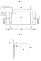
- FIG. 1 is a schematic block diagram illustrating a display device
- FIG. 2 is a diagram illustrating a sub-pixel shown in FIG. 1 .
- a display device includes a display panel 100, a timing controller 110, a data driver 120, and a scan driver 130, 140A, and 140B.
- the display panel 100 includes sub-pixels that are connected to each other and respectively distinguished by data lines DL and scan lines GL which intersect the data lines DL.
- the display panel 100 is sealed so as to protect at least one film, a substrate, or sub-pixels formed thereon from outdoor air such as moisture and oxygen.
- the display panel 100 includes a display area AA, on which sub-pixels are formed, and non-display areas LNA and RNA which is disposed lateral to the display area AA and on which various signal lines or pads are formed.
- the display panel 100 may be implemented by a top-emission method, a bottom-emission method, or a dual-emission method, depending on the configuration of sub-pixels SP.
- one sub-pixel SP includes a switching transistor SW connected to a scan line GL1 and a data line DL1, and a pixel circuit PC operating in response to a data signal DATA which is supplied in response to a scan signal supplied through the switching transistor SW.
- the pixel circuit PC of the sub pixel SP may be formed to further include a drive transistor, a storage capacitor, an organic light diode (OLED), and various types of compensation circuits.
- the timing controller 110 may receive timing signals through an LDVS or TMDS interface receiver circuit connected to a video board.
- the timing signals may include vertical a synchronization signal, a horizontal synchronization signal, a data enable signal, and a dot clock. With reference to an input timing signal, the timing controller 110 generates timing control signals for controlling operation timing of the data driver 120 and the scan driver.
- the data driver 120 includes a plurality of source drive Integrated Circuits (ICs).
- the source drive ICs are supplied with a data signal DATA and a source timing control signal DDC from the timing controller 110.
- the source drive ICs convert the form of the data signal DATA from a digital signal into an analog signal in response to the source timing control signal, and supplies the analog signal through the data lines DL of the display panel 100.
- the source drive ICs are connected to the data lines DL of the display panel 100 by a Chip On Glass (COG) process or a Tape Automated Bonding (TAB) process.
- COG Chip On Glass
- TAB Tape Automated Bonding
- the scan driver includes a level shifter circuit 130, and signal generation circuit 140A and 140B.
- the level shifter circuit 130 may be referred to as a power supply unit. Thus, the level shifter circuit 130 may be defined as an independent component not included in the scan driver. In the following description, however, the level shifter circuit 130 is depicted as being included in the scan driver for convenience of explanation.
- the level shifter circuit 130 is formed on an external substrate connected in the form of an IC to the display panel 100. Under the control of the timing controller 110, the level shifter circuit 130 may shift a level of a signal or voltage which is supplied through a clock signal line, a start signal line, a gate high voltage line, and a gate low voltage line. Then, the level shifter circuit 130 supplies the level-shifted signal or voltage to the signal generation circuit 140A and 140B.
- the signal generation circuit 140A and 140B is formed in the form of a Thin Film Transistor (TFT) on the display panel 100 in a Gate In Panel (GIP) method.
- the signal generation circuit 140A and 140B is formed on the left-hand non-display area LNA and the right-hand non-display area RNA of the display panel 100.
- the signal generation circuit 140A and 140B is composed of stages which shift and output a scan signal based on a signal or voltage CLK, ECLK, VST, EVST, RST, ERST, VGH, or VGL output from the level shifter circuit.
- the signal generation circuit 140A and 140B may be configured in various ways with signal lines and voltage lines along which the signal or voltage CLK, ECLK, VST, EVST, RST, ERST, VGH, or VGL is output bypassing the data driver.
- the signal generation circuit 140A and 140B includes a scan signal generation circuit 140A for outputting a scan signal for turning on or off switching transistors included in sub-pixels, and an emission signal generation circuit 140B for outputting an emission signal for turning on or off emission control transistors included in the sub-pixels.
- the scan signal generation circuit 140A and the emission signal generation circuit 140B may be arranged opposite to the case shown in FIG. 1 .
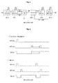
- FIG. 3 is a schematic block diagram illustrating part of an existing scan driver
- FIG. 4 is a waveform view illustrating input and output waveforms of an emission signal generation circuit shown in FIG. 3 .
- a signal generation circuit 140A and 140B of an existing scan driver includes a scan signal generation circuit 140A for outputting a scan signal for turning on or off switching transistors included in sub-pixels PXL, and an emission signal generation circuit 140B for outputting an emission signal for turning on or off emission control transistors included in the sub-pixels PXL.
- Sub-pixels PXL existing on one line Line 1 operate based on a first scan signal Scan 1 Out output from the first shift register SR[1], a second scan signal Scan 2 Out output from the second shift register SR[2], and an emission signal EM Out output from the first inverter circuit INV[1].
- the emission signal generation circuit 140B outputs the emission signal EM Out based on an output signal from a pull-down transistor of the third shift register SR[3] and an output signal from a pull-up transistor of the fourth shift register SR[4].
- the emission signal generation circuit 140B forms a rising edge of a signal output from itself, by synchronizing with a rising edge of an output signal GIP4 output from a pull-up transistor of the fourth shift register SR[4]. Then, the emission signal generation circuit 140B forms a falling edge with regard to a signal output from itself, by synchronizing with a rising edge of an output signal GIP3 Out from the pull-down transistor of the third shift register SR[3].
- the emission signal generation circuit 140B needs to vary the output signal GIP4 Out from the pull-up transistor of the fourth shift register SR[4] in order to perform variation PWM of a pulse width of the emission signal EM Out output from the emission signal generation circuit 140B.
- the signal generation circuit 140A and 140B of the existing scan driver includes four shift registers and a single inverter in order to drive sub-pixels existing on a single line Line 1.
- the emission signal generation circuit 140B needs to further include two additional shift registers in order to generate an emission signal EM Out to increase circuit complexity and layout limitation.
- the existing scan driver is difficult to secure the design margin due to the circuit complexity and layout limitation, so it is hard to implement a narrow bezel.
- FIG. 5 is a schematic block diagram illustrating part of a scan driver according to a first embodiment of the present disclosure
- FIG. 6 is a diagram illustrating an emission signal generation circuit according to the first embodiment of the present disclosure
- FIG. 7 is a waveform view illustrating input and output waves of the emission signal generation circuit shown in FIG. 6
- FIG. 8 is a simulation waveform view of a scan driver according to the first embodiment of the present disclosure
- FIG. 9 shows a waveform view of pulse-width modulation and outputs of the emission signal generation circuit according to the first embodiment of the present disclosure
- FIG. 10 is a diagram of the emission signal generation circuit according to an exemplary variation of the first embodiment of the present disclosure.
- a signal generation circuit 140A and 140B of a scan driver includes a scan signal generation circuit 140A for outputting a scan signal for turning on or off switching transistors included in sub-pixels PXL, and a emission signal generation circuit 140B for outputting an emission signal for turning on or off emission control transistors included in the sub-pixels PXL.
- the scan signal generation circuit 140A includes first and second register circuits SR[1] and SR[2] to receive a clock signal CLK and generate sequential scan signals based on the clock signal CLK.
- the emission signal generation circuit 140B includes a N-th EM driver EMD[N] to receive a clock signal ECLK and generate an emission signal based on the clock signal ECLK.
- the above configurations of the scan signal generation circuit 140A and the emission signal generation circuit 140B are arranged in the form of multiple stages in order to drive sub-pixels PXL existing on each line.
- Sub-pixels existing on one line Line 1 operate based on a first scan signal Scan 1 Out output from the first shift register SR[1], a second scan signal Scan 2 Out output from the second shift register SR[2], and a N-th emission signal EM[N] Out output from the N-th EM driver EMD[N].
- the signal generation circuit 140A and 140B of the scan driver includes two shift registers and a single EM driver in order to drive the sub-pixels PXL existing on one line Line 1.
- the shift registers are connected dependently.
- the emission signal generation circuit 140B does not need an additional shift register to generate an emission signal EM out, and it may help reduce circuit complexity and layout limitation, compared to the configuration of the existing scan driver.
- the emission signal generation circuit 140B is configured to generate the N-th emission signal EM[N] Out based on the clock signal ECLK and an output signal Scan1 Out output from the first shift register SR[1] of the scan signal generation circuit 140A.
- the emission signal generation circuit 140B uses the output signal Scan1 Out output from the first shift register SR[1] disposed on the opposite side to that of that of the existing scan driver.
- the output signal Scan1 Out output from the first shift register SR[1] is supplied to the emission signal generation circuit 140B through the display area AA.
- the second shift register SR[2] is disposed on a line on which the first shift register SR[1] is disposed, as illustrated in FIG. 5 . That is, the second shift register SR[2] and the first shift register SR[1] drives the same line.
- the emission signal generation circuit 140B may operate based on an output signal of a (N-x)-th shift register located before the first register circuit (x is an integer equal to or greater than 1). In the following description, however, the emission signal generation circuit 140B is depicted as operating in response to an output signal of the N-th shift register and a clock signal.
- the emission signal generation circuit 140B includes a first circuit EMDa for controlling charging and discharging of a Q node Q-node and a QB node QB-node, a second circuit EMDb for controlling charging and discharging of the Q node Q-node and the QB node QB-node, and a third circuit EMDc for outputting a Logic High or Logic Low emission signal through an output terminal EMO of the emission signal generation circuit 140B.
- EMDa for controlling charging and discharging of a Q node Q-node and a QB node QB-node
- a second circuit EMDb for controlling charging and discharging of the Q node Q-node and the QB node QB-node
- a third circuit EMDc for outputting a Logic High or Logic Low emission signal through an output terminal EMO of the emission signal generation circuit 140B.
- the first circuit EMDa includes a first transistor T1, a second transistor T2, a first capacitor CE, a third transistor A T3a, and a third transistor B T3b.
- the first transistor T1 is configured to charge the Q node Q-node to a potential of a start signal in response to a clock signal.
- the start signal may be replaced by a signal output through the output terminal of the emission signal generation circuit, which is disposed at a previous stage.
- the second transistor T2 is configured to transmit a gate low voltage to the other end of the first capacitor CE in response to the start signal.
- the other end of the first capacitor CE may be defined as a Q2 node Q2-node.
- the first capacitor CE is configured to turn on the third transistor A T3a by using bootstrap of a clock signal (in other words, by synchronizing with the clock signal).
- the third transistor A T3a is configured to charge or discharge the QB node QB-node to a potential of the clock signal in response to a potential of the Q2 node Q2-node.
- the third transistor B T3b is configured to discharge the QB node to the gate low voltage in response to a potential of the Q node Q-node.
- the third transistor A T3a is configured such that a gate electrode thereof is connected to the Q2 node Q2-node, a first electrode thereof is connected to the N-th clock signal line ECLK1, and a second electrode thereof is connected to the QB node QB-node.
- the third transistor B T3b is configured such that a gate electrode thereof is connected to the Q node Q-node, a first electrode is connected to the gate low voltage line VGL, and a second electrode thereof is connected to the QB node QB-node.
- the second circuit EMDb includes a fourth transistor T4 and a fifth transistor T5.
- the fourth transistor T4 is configured to charge or discharge the Q node Q-node to a potential of a reset signal in response to an output signal of the N-th shift register.
- the fifth transistor T5 is configured to charge or discharge the QB node QB-node to a potential to a clock signal in response to an output signal of the N-th shift register.
- the fourth transistor T4 is configured such that a gate electrode thereof is connected to an output terminal SRO of the N-th shift register, a first electrode thereof is connected to a reset signal line ERST, and a second electrode thereof is connected to the Q node Q-node.
- the fifth transistor T5 is configured such that a gate electrode thereof is connected to the output terminal SRO of the N-th shift register, a first electrode thereof is connected to the N-th clock signal line ECLK1, and a second electrode thereof is connected to the QB node QB-node.
- the third circuit EMDc includes a pull-up transistor Tpu, a pull-down transistor Tpd, and a second capacitor CB.
- the pull-up transistor Tpu is configured to output a gate high voltage through the output terminal EM Out of the emission signal generation circuit 140B in response to a potential of the Q node Q-node.
- the pull-down transistor Tpd is configured to output a gate low voltage through the output terminal EM Out of the emission signal generation circuit 140B in response to a potential of the QB node QB-node.
- the second capacitor CB is configured to cause bootstrap to occur in the output terminal EM Out of the emission signal generation circuit 140B.
- the pull-up transistor Tpu is configured such that a gate electrode thereof is connected to the Q node Q-node, a first electrode thereof is connected to a gate high voltage line VGH, and a second electrode thereof is connected to the output terminal EM Out of the emission signal generation circuit 140B.
- the pull-down transistor Tpd is configured such that a gate electrode thereof is connected to the QB node, a first electrode thereof is connected to the gate low voltage line VGL, and a second electrode thereof is connected to the output terminal EM Out of the emission signal generation circuit 140B.
- the second capacitor CB is configured such that one end thereof is connected to the Q node Q-node and the other end thereof is connected to the output terminal EM Out of the emission signal generation circuit 140B.
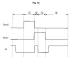
- the emission signal generation circuit may output emission signals EM_OUT1 to EM_OUT4 that are sequentially output for each line in response to a start signal EVST, a first clock signal ECLK1, a second clock signal ECLK2, and a reset signal ERST.
- a pulse width of an emission signal EM Out output from the emission signal generation circuit simply by adjusting a pulse width of a start signal EVST which is one of clock signals.
- a pulse width of the emission signal EM Out output from the emission signal generation circuit is adjusted such that the QB node is maintained at Logic High or Logic Low depending on a logic state of the start signal EVST.
- the emission signal generation circuit according to the exemplary variation of the first embodiment of the present disclosure further includes a sixth transistor T6 in the first circuit EMDa and a seventh transistor T7 in the third circuit EMDc.
- the sixth transistor T6 is configured such that a gate electrode thereof is connected to the start signal line EVST, a first electrode thereof is connected to the gate low voltage line VGL, and a second electrode thereof is connected to the QB node QB-node.
- the seventh transistor T7 is configured such that a gate electrode thereof is connected to the gate high voltage line VGH, a first electrode thereof is connected to one side of the Q node Q-node being adjacent to the second electrode of the fourth transistor T4, and a second electrode thereof is connected to the other side of the Q node Q-node being adjacent to one end of the second capacitor CB.
- the first transistor T1 is configured such that a gate electrode thereof is connected to a N-th clock signal line (which is depicted as a first clock signal line ECLK1 in the embodiment), a first electrode thereof is connected to a start signal line (which is depicted as an emission signal generation circuit existing in the first stage), and a second electrode thereof is connected to the Q node Q-node.
- the second transistor T2 is configured such that a gate electrode thereof is connected to the start signal line, a first electrode thereof is connected to a gate low voltage line VGL, and a second electrode is connected to the Q2 node Q2-node.
- the first capacitor CE is configured such that one end thereof is connected to the clock signal line ECLK1 and the other end thereof is connected to the Q2 node Q2-node.
- the third transistor A T3a is configured such that a gate electrode thereof is connected to the Q2 node Q2-node, a first electrode thereof is connected to the N-th clock signal line ECLK1, and a second electrode thereof is connected to the QB node QB-node.
- the third transistor B T3b is configured such that a gate electrode thereof is connected to the Q node Q-node, a first electrode thereof is connected to the gate low voltage line VGL, and a second electrode thereof is connected to the QB node QB-node.
- the second circuit EMDb includes a fourth transistor T4 and a fifth transistor T5.
- the fourth transistor T4 is configured to charge or discharge the Q node Q-node to a potential to a reset signal in response to an output signal of the N-th shift register.
- the fifth transistor T5 is configured to charge or discharge the QB node to a potential of a clock signal in response to the output signal of the N-th shift register.
- the third circuit EMDc includes a pull-up transistor Tpu, a first pull-down transistor Tpda, a second pull-down transistor Tpdb, a second capacitor CB, the seventh transistor T7, and an eighth transistor T8.
- the pull-up transistor Tpu is configured to output a gate high voltage through an output terminal EM Out of the emission signal generation circuit 140B in response to a potential of the Q node Q-node.
- the first and second pull-down transistors Tpda and Tpdb are each configured to output a gate low voltage through the output terminal EM Out of the emission signal generation circuit 140B in response to a potential of the QB node QB-node.
- the pull-up transistor Tpu is configured such that a gate electrode thereof is connected to the Q node Q-node, a first electrode thereof is connected to the gate high voltage line VGH, and a second electrode thereof is connected to the output terminal EM Out of the emission signal generation circuit 140B.
- the first pull-down transistor Tpda is configured such that a gate electrode thereof is connected to the QB node QB-node, a first electrode thereof is connected to a second electrode of the second pull-down transistor Tpdb, and a second electrode thereof is connected to the output terminal EM Out of the emission signal generation circuit 140B.
- the second pull-down transistor Tpdb is configured such that a gate electrode thereof is connected to the QB node QB-node, a first electrode thereof is connected to the gate low voltage line VGL, and a second electrode thereof is connected to the first electrode of the first pull-down transistor Tpda.
- the second capacitor CB is configured such that one end thereof is connected to the Q node Q-node and the other end thereof is connected to the output terminal EM Out of the emission signal generation circuit 140B.
- the seventh transistor T7 is configured such that a gate electrode thereof is connected to the gate high voltage line VGH, a first electrode thereof is connected to the second electrode of the fourth transistor T4, and a second electrode thereof is connected to the Q node Q-node, and via the Q node to one end of the second capacitor CB and the gate electrode of the pull up transistor Tpu.
- the eighth transistor T8 is configured such that a gate electrode thereof is connected to the output terminal EM Out of the emission signal generation circuit 140B, a first electrode thereof is connected to the gate high voltage line VGH, and a second electrode thereof is connected to a node located between the first electrode of the first pull-down transistor Tpda and the second electrode of the second pull-down transistor Tpdb.
- FIG. 12 is a diagram illustrating an emission signal generation circuit according to a third embodiment of the present disclosure.
- the first circuit EMDa includes a first transistor T1, a second transistor T2, a first capacitor CE, a third transistor A T3a, and a third transistor B T3b.
- the first transistor T2 is configured to charge the Q node Q-node to a potential of a start signal in response to a clock signal.
- the start signal may be replaced by a signal output through an output terminal of the emission signal generation circuit which is located at a previous stage.
- the second transistor T2 is configured to transmit a gate low voltage to the other end of the first capacitor CE in response to the start signal.
- the other end of the first capacitor CE may be defined as a Q2 node Q2-node.
- the first capacitor CE is configured to turn on the third transistor A T3a by using bootstrap of a clock signal (in other words, by synchronizing with the clock signal).
- the third transistor A T3a is configured to charge or discharge the QB node QB-node to potential of the clock signal in response to a potential of the Q2 node Q2-node.
- the third transistor B T3b is configured to discharge the QB node to the gate low voltage in response to a potential of the Q node Q-node.
- the first transistor T1 is configured such that a gate electrode thereof is connected to a N-th clock signal line (which is depicted as a first clock signal line ECLK1 in the embodiment), a first electrode thereof is connected to a start signal line (which is depicted as an emission signal generation circuit existing in a first stage), and a second electrode thereof is connected to the Q node Q-node.
- the second transistor T2 is configured such that a gate electrode thereof is connected to the start signal line, a first electrode thereof is connected to a gate low voltage line VGL, and a second electrode thereof is connected to the Q2 node Q2-node.
- the first capacitor CE is configured such that one end thereof is connected to the clock signal line ECLK1 and the other end thereof is connected to the Q2 node Q2-node.
- the third transistor A T3a is configured such that a gate electrode thereof is connected to the Q2 node Q2-node, a first electrode thereof is connected to the N-th clock signal line ECLK1, and a second electrode thereof is connected to the QB node QB-node.
- the third transistor B T3b is configured such that a gate electrode thereof is connected to the Q node Q-node, a first electrode thereof is connected to the gate low voltage line VGL, and a second electrode thereof is connected to the QB node QB-node.
- the second circuit EMDb includes a fourth transistor T4, a fifth transistor T5, and a third capacitor CQB.
- the fourth transistor T4 is configured to charge or discharge the Q node Q-node to a potential of a reset signal in response to an output signal of the N-th shift register.
- the fifth transistor T5 is configured to charge or discharge the QB node QB-node to a potential to a clock signal in response to an output signal of the N-th shift register.
- the third capacitor CQB is configured to maintain a potential of the QB node QB-node at Logic High or Logic Low so that an emission signal can be stably output through the output terminal EMO of the emission signal generation circuit 140B.
- the fourth transistor T4 is configured such that a gate electrode thereof is connected to an output terminal SRO of the N-th shift register, a first electrode thereof is connected to a reset signal line ERST, and a second electrode thereof is connected to the Q node Q-node.
- the fifth transistor T5 is configured such that a gate electrode thereof is connected to the output terminal SRO of the N-th shift register, a first electrode thereof is connected to the N-th clock signal line ECLK1, and a second electrode thereof is connected to the QB node QB-node.
- the third capacitor CQB is configured such that one end thereof is connected to the QB node QB-node and the other end thereof is connected to the gate low voltage line VGL.
- the third circuit EMDc includes a pull-up transistor Tpu, a first pull-down transistor Tpda, a second pull-down transistor Tpdb, a second capacitor CB, and an eighth transistor T8.
- the pull-up transistor Tpu is configured to output a gate high voltage through an output terminal EM Out of the emission signal generation circuit 140B in response to a potential of the Q node Q-node.
- the first and second pull-down transistors Tpda and Tpdb are each configured to output a gate low voltage in response to a potential of the QB node QB-node through the output terminal EM Out of the emission signal generation circuit 140B.
- the second capacitor CB is configured to cause bootstrap to occur in the output terminal EM Out of the emission signal generation circuit 140B.
- the eighth transistor T8 is configured to stabilize a node connected to electrodes of the pull-down transistors Tpda and Tpdb in response to a potential of the output terminal EM Out of the emission signal generation circuit 140B.
- the second pull-down transistor Tpdb is configured such that a gate electrode thereof is connected to the QB node QB-node, a first electrode thereof is connected to the gate low voltage line VGL, and a second electrode thereof is connected to the first electrode of the first pull-down transistor Tpda.
- the second capacitor CB is configured such that one end thereof is connected to the Q node Q-node and the other end thereof is connected to the output terminal EM Out of the emission signal generation circuit 140B.
- the eighth transistor T8 is configured such that a gate electrode thereof is connected to the output terminal EM Out of the emission signal generation circuit 140B, a first electrode thereof is connected to the gate high voltage line VGH, and a second electrode thereof is connected to a node located between the first electrode of the first pull-down transistor Tpda and the second electrode of the second pull-down transistor Tpdb.
- FIG. 13 is a diagram illustrating an emission signal generation circuit according to a fourth embodiment of the present disclosure.
- an emission signal generated circuit 140B includes a first circuit EMDa for controlling charging and discharging of a Q node Q-node and a QB node QB-node, a second circuit EMDb for controlling charging and discharging of the Q node Q-node and the QB node QB-node, and a third circuit EMDc for controlling a Logic High or Logic Low emission signal through an output terminal EMO of the emission signal generation circuit 140B.
- the first circuit EMDa includes a first transistor T1, a second transistor T2, a first capacitor CE, a third transistor A T3a, and a third transistor B T3b.
- the first transistor T2 is configured to charge the Q node Q-node to a potential of a start signal in response to a clock signal.
- the start signal may be replaced by a signal output through an output terminal of the emission signal generation circuit which is located at a previous stage.
- the second transistor T2 is configured to transmit a gate low voltage to the other end of the first capacitor CE in response to the start signal.
- the other end of the first capacitor CE may be defined as a Q2 node Q2-node.
- the first capacitor CE is configured to turn on the third transistor A T3a by using bootstrap of a clock signal (in other words, by synchronizing with the clock signal).
- the third transistor A T3a is configured to charge or discharge the QB node QB-node to a potential of the clock signal in response to a potential of the Q2 node Q2-node.
- the third transistor B T3b is configured to discharge the QB node to a gate low voltage in response to a potential of the Q node Q-node.
- the first transistor T1 is configured such that a gate electrode thereof is connected to a N-th clock signal line (which is depicted as a first clock signal line ECLK1 in embodiments), a first electrode thereof is connected to a start signal line (which is depicted as an emission signal generation circuit existing in a first stage), and a second electrode thereof is connected to the Q node Q-node.
- the second transistor T2 is configured such that a gate electrode thereof is connected to the start signal line, a first electrode thereof is connected to a gate low voltage line VGL, and a second electrode thereof is connected to the Q2 node Q2-node.
- the first capacitor CE is configured such that one end thereof is connected to the clock signal line ECLK1 and the other end thereof is connected to the Q2 node Q2-node.
- the third transistor A T3a is configured such that a gate electrode thereof is connected to the Q2 node Q2-node, a first electrode thereof is connected to the N-th clock signal line ECLK1, and a second electrode thereof is connected to the QB node QB-node.
- the third transistor B T3b is configured such that a gate electrode thereof is connected to the Q node Q-node, a first electrode thereof is connected to the gate low voltage line VGL, and a second electrode thereof is connected to the QB node QB-node.
- the second circuit EMDb includes fourth transistors T4a to T4c, a fifth transistor T5, and a third capacitor CQB.
- the fourth transistors T4a to T4c are each configured to charge the Q node Q-node to a gate high voltage in response to an output signal of the N-th shift register and a gate high voltage.
- the fifth transistor T5 is configured to charge or discharge the QB node QB-node to a potential to a clock signal in response to an output signal of the N-th shift register.
- the third capacitor CQB is configured to maintain a potential of the QB node QB-node at Logic High or Logic Low so that an emission signal can be stably output through the output terminal EMO of the emission signal generation circuit 140B.
- the fourth transistor A T4a is configured such that a gate electrode thereof is connected to an output terminal SRO of the N-th shift register, a first electrode thereof is connected to a gate high voltage line VGH, and a second electrode thereof is connected to a first electrode of a fourth transistor B T4b.
- the fourth transistor B T4b is configured such that a gate electrode thereof is connected to a second electrode of the fourth transistor C T4c, a first electrode thereof is connected to the second electrode of the fourth transistor A T4a, and a second electrode thereof is connected to the Q node Q-node.
- the fourth transistor C T4c is configured such that a gate electrode thereof is connected to the gate high voltage line VGH, a first electrode thereof is connected to a reset signal line ERST, and a second electrode thereof is connected to the gate electrode of the fourth transistor B T4b.
- the fifth transistor T5 is configured such that a gate electrode thereof is connected to the second electrode of the fourth transistor C T4c (or the gate electrode of the fourth transistor B T4b), a first electrode thereof is connected to the N-th clock signal line ECLK1, and a second electrode is connected to the QB node QB-node.
- the third capacitor CQB is configured such that one end thereof is connected to the QB node QB-node and the other end thereof is connected to the gate low voltage line VGL.
- the third circuit EMDc includes a pull-up transistor Tpu, a first pull-down transistor Tpda, a second pull-down transistor Tpdb, a second capacitor CB, and an eighth transistor T8.
- the pull-up transistor Tpu is configured to output a gate high voltage through an output terminal EM Out of the emission signal generation circuit 140B in response to a potential of the Q node Q-node.
- the first and second pull-down transistors Tpda and Tpdb are each configured to output a gate low voltage in response to a potential of the QB node QB-node through the output terminal EM Out of the emission signal generation circuit 140B.
- the second capacitor CB is configured to cause bootstrap to occur in the output terminal EM Out of the emission signal generation circuit 140B.
- the eighth transistor T8 is configured to stabilize nodes connected to electrodes of the pull-down transistors Tpda and Tpdb in response to a potential of the output terminal EM Out of the emission signal generation circuit 140B.
- the pull-up transistor Tpu is configured such that a gate electrode thereof is connected to the Q node Q-node, a first electrode thereof is connected to the gate high voltage line VGH, and a second electrode thereof is connected to the output terminal EM Out of the emission signal generation circuit 140B.
- the first pull-down transistor Tpda is configured such that a gate electrode thereof is connected to the QB node QB-node, a first electrode thereof is connected to a second electrode of the second pull-down transistor Tpdb, and a second electrode thereof is connected to the output terminal EM Out of the emission signal generation circuit 140B.
- the eighth transistor T8 is configured such that a gate electrode thereof is connected to the output terminal EM Out of the emission signal generation circuit 140B, a first electrode thereof is connected to the gate high voltage line VGH, and a second electrode thereof is connected to a node located between the first electrode of the first pull-down transistor Tpda and the second electrode of the second pull-down transistor Tpdb.
- FIG. 14 is a diagram illustrating an emission signal generation circuit according to a fifth embodiment of the present disclosure.
- an emission signal generated circuit 140B includes a first circuit EMDa for controlling charging and discharging of a Q node Q-node and a QB node QB-node, a second circuit EMDb for controlling charging and discharging of the Q node Q-node and the QB node QB-node, and a third circuit EMDc for outputting a Logic-High or Logic-Low emission signal through an output terminal EMO of the emission signal generation circuit 140B.
- the first circuit EMDa includes a first transistor T1, a second transistor T2, a first capacitor CE, a third transistor A T3a, and a third transistor B T3b.
- the first transistor T1 is configured to charge the Q node Q-node to a potential of a start signal in response to a clock signal.
- the start signal may be replaced by a signal output through an output terminal of the emission signal generation circuit which is located at a previous stage.
- the second transistor T2 is configured to transmit a gate low voltage to the other end of the first capacitor CE in response to the start signal.
- the other end of the first capacitor CE may be defined as a Q2 node Q2-node.
- the first capacitor CE is configured to turn on the third transistor A T3a by using bootstrap of a clock signal (in other words, by synchronizing with the clock signal).
- the third transistor A T3a is configured to charge or discharge the QB node QB-node to potential of the clock signal in response to a potential of the Q2 node Q2-node.
- the third transistor B T3b is configured to discharge the QB node to a gate low voltage in response to a potential of the Q node Q-node.
- the first transistor T1 is configured such that a gate electrode thereof is connected to a N-th clock signal line (which is depicted as a first clock signal line ECLK1 in embodiments), a first electrode thereof is connected to a start signal line (which is depicted as an emission signal generation circuit existing in a first stage), and a second electrode thereof is connected to the Q node Q-node.
- the second transistor T2 is configured such that a gate electrode thereof is connected to the start signal line, a first electrode thereof is connected to a gate low voltage line VGL, and a second electrode thereof is connected to the Q2 node.
- the first capacitor CE is configured such that one end thereof is connected to the clock signal line ECLK1 and the other end thereof is connected to the Q2 node Q2-node.
- the third transistor A T3a is configured such that a gate electrode thereof is connected to the Q2 node Q2-node, a first electrode thereof is connected to the N-th clock signal line ECLK1, and a second electrode thereof is connected to the QB node QB-node.
- the third transistor B T3b is configured such that a gate electrode thereof is connected to the Q node Q-node, a first electrode is connected to the gate low voltage line VGL, and a second electrode thereof is connected to the QB node QB-node.
- the second circuit EMDb includes fourth transistors T4a and T4b, a fifth transistor T5, and a third capacitor CQB.
- the fourth transistors T4a and T4b are each configured to charge the Q node Q-node to a gate high voltage in response to an output signal of a N-th shift register and a reset signal.
- the fifth transistor T5 is configured to charge or discharge the QB node QB-node to a potential to a clock signal in response to an output signal of the N-th shift register.
- the third capacitor CQB is configured to maintain a potential of the QB node QB-node at Logic High or Logic Low so that an emission signal can be stably output through the output terminal EMO of the emission signal generation circuit 140B.
- a fourth transistor A T4a is configured such that a gate electrode thereof is connected to an output terminal SRO of the N-th shift register, a first electrode thereof is connected to a gate high voltage line VGH, and a second electrode thereof is connected to a first electrode of a fourth transistor B T4b.
- the fourth transistor B T4b is configured such that a gate electrode thereof is connected to a reset signal line ERST, a first electrode thereof is connected to the second electrode of the fourth transistor A T4a, and a second electrode thereof is connected to the Q node Q-node.
- the fifth transistor T5 is configured such that such that a gate electrode thereof is connected to the reset signal line ERST, a first electrode thereof is connected to a N-th clock signal line ECLK1, and a second electrode thereof is connected to the QB node QB-node.
- the third capacitor CQB is configured such that one end thereof is connected to the QB-node and the other end thereof is connected to the gate low voltage line VGL.
- the third circuit EMDc includes a pull-up transistor Tpu, a first pull-down transistor Tpda, a second pull-down transistor Tpdb, a second capacitor CB, and an eighth transistor T8.
- the pull-up transistor Tpu is configured to output a gate high voltage through an output terminal EM Out of the emission signal generation circuit 140B in response to a potential of the Q node Q-node.
- the first and second pull-down transistors Tpda and Tpdb are each configured to output a gate low voltage through the output terminal EM Out of the emission signal generation circuit 140B in response to a potential of the QB node QB-node.
- the second capacitor CB is configured to cause bootstrap to occur in the output terminal EM Out of the emission signal generation circuit 140B.
- the eighth transistor T8 is configured to stabilize a node connected to electrodes of the pull-down transistors Tpda and Tpdb in response to a potential of the output terminal EM Out of the emission signal generation circuit 140B.
- the second pull-down transistor Tpdb is configured such that a gate electrode thereof is connected to the QB node QB-node, a first electrode thereof is connected to the gate low voltage line VGL, and a second electrode thereof is connected to the first electrode of the first pull-down transistor Tpda.
- the second capacitor CB is configured such that one end thereof is connected to the Q node Q-node and the other end thereof is connected to the output terminal EM Out of the emission signal generation circuit 140B.
- the eighth transistor T8 is configured such that a gate electrode thereof is connected to the output terminal EM Out of the emission signal generation circuit 140B, a first electrode thereof is connected to the gate high voltage line VGH, and a second electrode thereof is connected to a node located between the first electrode of the first pull-down transistor Tpda and the second electrode of the second pull-down transistor Tpdb.
- FIG. 15 is a diagram illustrating an emission signal generation circuit according to a sixth embodiment of the present disclosure.
- an emission signal generated circuit 140B includes a first circuit EMDa for controlling charging and discharging of a Q node Q-node and a QB node QB-node, a second circuit EMDb for controlling charging and discharging of the Q node Q-node and the QB node QB-node, and a third circuit EMDc for outputting a Logic-High or Logic-Low emission signal through an output terminal EMO of the emission signal generation circuit 140B.
- the first circuit EMDa includes a first transistor T1, a second transistor T2, a first capacitor CE, a third transistor A T3a, and a third transistor B T3b.
- the first transistor T1 is configured to charge the Q node Q-node to a potential of a start signal in response to a clock signal.
- the start signal may be replaced by a signal output through an output terminal of the emission signal generation circuit which is located at a previous stage.
- the second transistor T2 is configured to transmit a gate low voltage to the other end of the first capacitor CE in response to the start signal.
- the other end of the first capacitor CE may be defined as a Q2 node Q2-node.
- the first capacitor CE is configured to turn on the third transistor A T3a by using bootstrap of a clock signal (in other words, by synchronizing with the clock signal).
- the third transistor A T3a is configured to charge or discharge the QB node QB-node to a potential of the clock signal in response to a potential of the Q2 node Q2-node.
- the third transistor B T3b is configured to discharge the QB node to a gate low voltage in response to a potential of the Q node Q-node.
- the first transistor T1 is configured such that a gate electrode thereof is connected to a N-th clock signal line (which is depicted as a first clock signal line ECLK1 in embodiments), a first electrode thereof is connected to a start signal line (which is depicted as an emission signal generation circuit existing in a first stage), and a second electrode thereof is connected to the Q node Q-node.
- the second transistor T2 is configured such that a gate electrode thereof is connected to the start signal line, a first electrode thereof is connected to a low voltage line VGL, and a second electrode thereof is connected to the Q2 node Q2-node.
- the first capacitor CE is configured such that one end thereof is connected to the clock signal line ECLK1 and the other end thereof is connected to the Q2 node Q2-node.
- the third transistor A T3a is configured such that a gate electrode thereof is connected to the Q2 node Q2-node, a first electrode thereof is connected to the N-th clock signal line ECLK1, and a second electrode thereof is connected to the QB node QB-node.
- the third transistor B T3b is configured such that a gate electrode thereof is connected to the Q node Q-node, a first electrode thereof is connected to the gate low voltage line VGL, and a second electrode thereof is connected to the QB node QB-node.
- the second circuit EMDb includes fourth transistors T4a to T4c, a fifth transistor T5, and a third capacitor CQB.
- the fourth transistors T4a to T4c are each configured to charge the Q node Q-node to a gate high voltage in response to an output signal of the N-th shift register and a gate high voltage.
- the fifth transistor T5 is configured to charge or discharge the QB node QB-node to a potential to a clock signal in response to an output signal of the N-th shift register.
- the third capacitor CQB is configured to maintain a potential of the QB node QB-node at Logic High or Logic Low so that an emission signal can be stably output through the output terminal EMO of the emission signal generation circuit 140B.
- the fourth transistor A T4a is configured such that a gate electrode thereof is connected to an output terminal SRO of the N-th shift register, a first electrode thereof is connected to a gate high voltage line VGH, and a second electrode thereof is connected to a first electrode of a fourth transistor B T4b.
- the fourth transistor B T4b is configured such that a gate electrode thereof is connected to a second electrode of the fourth transistor C T4c, a first electrode thereof is connected to the second electrode of the fourth transistor A T4a, and a second electrode thereof is connected to the Q node Q-node.
- the fourth transistor C T4c is configured such that a gate electrode thereof is connected to the gate high voltage line VGH, a first electrode thereof is connected to a reset signal line ERST, and a second electrode thereof is connected to the gate electrode of the fourth transistor B T4b.
- the fifth transistor T5 is configured such that a gate electrode thereof is connected to the output terminal SRO of the N-th shift register, a first electrode thereof is connected to the N-th clock signal line ECLK1, and a second electrode is connected to the QB node QB-node.
- the third capacitor CQB is configured such that one end thereof is connected to the QB node QB-node and the other end thereof is connected to the gate low voltage line VGL.
- the third circuit EMDc includes a pull-up transistor Tpu, a first pull-down transistor Tpda, a second pull-down transistor Tpdb, a second capacitor CB, and an eighth transistor T8.
- the pull-up transistor is Tpu configured to output a gate high voltage through an output terminal EM Out of the emission signal generation circuit 140B in response to a potential of the Q node Q-node.
- the first and second pull-down transistors Tpda and Tpdb are each configured to output a gate low voltage in response to a potential of the QB node QB-node through the output terminal EM Out of the emission signal generation circuit 140B.
- the second capacitor CB is configured to cause bootstrap to occur in the output terminal EM Out of the emission signal generation circuit 140B.
- the eighth transistor T8 is configured to stabilize a node connected to electrodes of the pull-down transistors Tpda and Tpdb in response to a potential of the output terminal EM Out of the emission signal generation circuit 140B.
- the pull-up transistor Tpu is configured such that a gate electrode thereof is connected to the Q node Q-node, a first electrode thereof is connected to the gate high voltage line VGH, and a second electrode thereof is connected to the output terminal EM Out of the emission signal generation circuit 140B.
- the first pull-down transistor Tpda is configured such that a gate electrode thereof is connected to the QB node QB-node, a first electrode thereof is connected to a second electrode of the second pull-down transistor Tpdb, and a second electrode thereof is connected to the output terminal EM Out of the emission signal generation circuit 140B.
- the second pull-down transistor Tpdb is configured such that a gate electrode thereof is connected to the QB node QB-node, a first electrode thereof is connected to the gate low voltage line VGL, and a second electrode thereof is connected to the first electrode of the first pull-down transistor Tpda.
- the second capacitor CB is configured such that one end thereof is connected to the Q node Q-node and the other end thereof is connected to the output terminal EM Out of the emission signal generation circuit 140B.
- the eighth transistor T8 is configured such that a gate electrode thereof is connected to the output terminal EM Out of the emission signal generation circuit 140B, a first electrode thereof is connected to the gate high voltage line VGH, and a second electrode thereof is connected to a node located between the first electrode of the first pull-down transistor Tpda and the second electrode of the second pull-down transistor Tpdb.
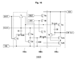
- FIG. 16 is a diagram illustrating an emission signal generation circuit according to a seventh embodiment of the present disclosure.
- an emission signal generated circuit 140B includes a first circuit EMDa for controlling charging and discharging of a Q node Q-node and a QB node QB-node, a second circuit EMDb for controlling charging and discharging of the Q node Q-node and the QB node QB-node, and a third circuit EMDc for outputting a Logic-High or Logic-Low emission signal through an output terminal EMO of the emission signal generation circuit 140B.
- the first circuit EMDa includes a first transistor T1, a second transistor T2, a first capacitor CE, a third transistor A T3a, and a third transistor B T3b.
- the first transistor T2 is configured to charge the Q node Q-node to a potential of a start signal in response to a clock signal.
- the start signal may be replaced by a signal output through an output terminal of the emission signal generation circuit which is located at a previous stage.
- the second transistor T2 is configured to transmit a gate low voltage to the other end of the first capacitor CE in response to the start signal.
- the other end of the first capacitor CE may be defined as a Q2 node Q2-node.
- the first capacitor CE is configured to turn on the third transistor A T3a by using bootstrap of a clock signal (in other words, by synchronizing with the clock signal).
- the third transistor A T3a is configured to charge or discharge the QB node QB-node to a potential of the clock signal in response to a potential of the Q2 node Q2-node.
- the third transistor B T3b is configured to discharge the QB node to a gate low voltage in response to a potential of the Q node Q-node.
- the first transistor T1 is configured such that a gate electrode thereof is connected to a N-th clock signal line (which is depicted as a first clock signal line ECLK1 in embodiments), a first electrode thereof is connected to a start signal line (which is depicted as an emission signal generation circuit existing in a first stage), and a second electrode thereof is connected to the Q node Q-node.
- the second transistor T2 is configured such that a gate electrode thereof is connected to the start signal line, a first electrode thereof is connected to a gate low voltage line VGL, and a second electrode thereof is connected to the Q2 node Q2-node.
- the first capacitor CE is configured such that one end thereof is connected to the clock signal line ECLK1 and the other end thereof is connected to the Q2 node Q2-node.
- the third transistor A T3a is configured such that a gate electrode thereof is connected to the Q2 node Q2-node, a first electrode thereof is connected to the N-th clock signal line ECLK1, and a second electrode thereof is connected to the QB node QB-node.
- the third transistor B T3b is configured such that a gate electrode thereof is connected to the Q node Q-node, a first electrode thereof is connected to the gate low voltage line VGL, and a second electrode thereof is connected to the QB node QB-node.
- the second circuit EMDb includes fourth transistors T4a to T4b, a fifth transistor T5, and a third capacitor CQB.
- the fourth transistors T4a to T4b are each configured to charge the Q node Q-node to a gate high voltage in response to an output signal of the N-th shift register and a reset signal.
- the fifth transistor T5 is configured to charge or discharge the QB node QB-node to a potential to a clock signal in response to an output signal of the N-th shift register.
- the third capacitor CQB is configured to maintain a potential of the QB node QB-node at Logic High or Logic Low so that an emission signal can be output through the output terminal EMO of the emission signal generation circuit 140B.
- the fourth transistor A T4a is configured such that a gate electrode thereof is connected to a reset signal line ERST, a first electrode thereof is connected to a gate high voltage line VGH, and a second electrode thereof is connected to a first electrode of a fourth transistor B T4b.
- the fourth transistor B T4b is configured such that a gate electrode thereof is connected to an output terminal SRO of the N-th shift register, a first electrode thereof is connected to the second electrode of the fourth transistor A T4a, and a second electrode thereof is connected to the Q node Q-node.
- the fifth transistor T5 is configured such that a gate electrode thereof is connected to the reset signal line ERST, a first electrode thereof is connected to the N-th clock signal line ECLK1, and a second electrode is connected to the QB node QB-node.
- the third capacitor CQB is configured such that one end thereof is connected to the QB node QB-node and the other end thereof is connected to the gate low voltage line VGL.
- the third circuit EMDc includes a pull-up transistor Tpu, a first pull-down transistor Tpda, a second pull-down transistor Tpdb, a second capacitor CB, and an eighth transistor T8.
- the pull-up transistor Tpu is configured to output a gate high voltage through an output terminal EM Out of the emission signal generation circuit 140B in response to a potential of the Q node Q-node.
- the first and second pull-down transistors Tpda and Tpdb are each configured to output a gate low voltage in response to a potential of the QB node QB-node through the output terminal EM Out of the emission signal generation circuit 140B.
- the eighth transistor T8 is configured such that a gate electrode thereof is connected to the output terminal EM Out of the emission signal generation circuit 140B, a first electrode thereof is connected to the gate high voltage line VGH, and a second electrode thereof is connected to a node located between the first electrode of the first pull-down transistor Tpda and the second electrode of the second pull-down transistor Tpdb.
- the above-described scan driver may be applied to a display device which is implemented by sub-pixels in the following circuit structure.
- FIG. 17 is a diagram illustrating details of a sub-pixel shown in FIG. 2
- FIG. 18 is a waveform view illustrating an output waveform of a scan driver according to the present disclosure and a node voltage of a driving transistor.
- a sub-pixel has a circuit structure including four transistors, two storage capacitors, and an OLED.
- the four transistors include a switching transistor SWT, an emission control transistor EMT, a driving transistor DRT, and a sensing transistor SNT.
- the two storage capacitors include a first storage capacitor CST and a second storage capacitor CDT.
- the switching transistor SWT is configured to transfer a reference voltage Ref or a data voltage Data to one end of the first storage capacitor CST.
- the switching transistor SWT is configured such that a gate electrode thereof is connected to a first scan line Scan1, a first electrode thereof is connected to a data line DL, and a second electrode thereof is connected to one end of the first storage capacitor CST and to a gate electrode of the driving transistor DRT.
- the driving transistor DRT is configured to generate a driving current in response to a data voltage stored in the first storage capacitor CST, the driving current which causes the OLED to emit light.
- the driving transistor DRT is configured such that a gate electrode thereof is connected to one end of the first storage capacitor CST, a first electrode thereof is connected to the second electrode of the emission control transistor EMT, and a second electrode thereof is connected to an anode electrode of the OLED.
- the sensing transistor SNT is configured to supply an initial voltage Vini to a sensing node so as not just to perform initialization, but to sense characteristics of the driving transistor DRT and the OLED (for example, a threshold voltage and current mobility).
- the sensing transistor SNT is configured such that a gate electrode thereof is connected to a second scan line Scan2, a first electrode thereof is connected to a sensing line SL, and a second electrode thereof is connected to the second electrode of the driving transistor DRT, to the anode electrode of the OLED, and to a sensing node connected to the first storage capacitor CST.
- the OLED is configured to emit light in response to a driving current generated by the driving transistor DRT.
- the OLED is configured such that an anode electrode thereof is connected to the sensing node and a cathode electrode thereof is connected to a second power line VSS.
- an emission signal em remains at Logic Low, and a second scan signal Scan 2 at a gate high voltage is output through an output terminal SRO[2] of a second shift register. Then, a sensing node (or a source node) of the driving transistor DRT is initialized to an initial voltage Vini (see Section 1).
- a scan signal Scan 1 at a gate low voltage is output through the output terinal SRO[N[ of the first shift register, and the emission signal em is changed to Logic High (a second emission signal). Then, the driving transistor DRT generates a driving current in response to the data voltage Data programmed to the first storage capacitor CST, and the OLED emits light in response to the driving current (see Section 4).
- the above-described sub-pixel needs an emission signal having at least two Logic High sections in order to perform sampling operation 2 and emission operation 4.
- An emission signal em in the emission operation 4 is generated by an emission signal generation circuit of a scan driver according to the first embodiment of the present disclosure.
- an emission signal em is generated having a first signal with a short Logic High section and a second signal with a Logic High section longer than that of the first signal.
- a Logic High section of the first scan signal Scan 1 partly overlaps a Logic High section of the second scan signal Scan 2
- the first Logic High section of the emission signal em overlaps the Logic Low section of the first scan signal Scan 1.
- the waveform shown in FIG. 18 is merely an example, and it may vary with a clock signal and a reset signal.
- the present disclosure may remove the need of an additional shift register provided in a display device to generate an emission signal, thereby reducing circuit complexity and layout limitation.
- the present disclosure may reduce circuit complexity of a scan driver to thereby overcome layout limitation and secure sufficient design margin, improving difficulties of implementing a narrow bezel.
- the present disclosure may reduce circuit complexity of a scan driver to thereby secure sufficient encapsulation margin, improving device reliability.
- the present disclosure is able to adjust a pulse width of an emission signal by means of a clock signal to thereby reduce a lateral current, adjusting an initial time sufficiently and thus enabling stable driving operation.
Landscapes
- Engineering & Computer Science (AREA)
- Power Engineering (AREA)
- Microelectronics & Electronic Packaging (AREA)
- Physics & Mathematics (AREA)
- Computer Hardware Design (AREA)
- General Physics & Mathematics (AREA)
- Theoretical Computer Science (AREA)
- Control Of Indicators Other Than Cathode Ray Tubes (AREA)
- Chemical & Material Sciences (AREA)
- Crystallography & Structural Chemistry (AREA)
- Control Of El Displays (AREA)
Abstract

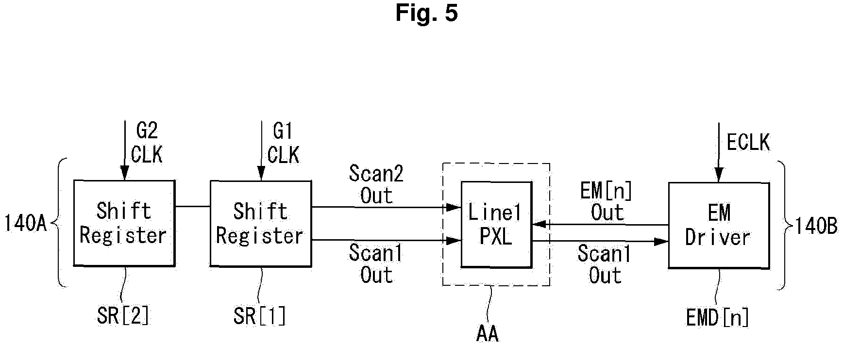
Description
- This application claims the priority benefit of
Korean Patent Application No. 10-2015-0147981, filed on October 23, 2015 - The present disclosure relates to a scan driver, a display device, and a method of driving the display device.
- With the development of information technologies, the display device market is growing. A display device is a medium which enables connection between a user and information. The display device includes an organic light emitting display (OLED), a liquid crystal display (LCD), a plasma display panel (PDP), etc, and it is being widely used these days.
- Some of the examples of the display device, such as the LCD or the OLED, operate in a manner that a selected sub-pixel emits light once a scan signal and a data signal is supplied to sub-pixels included in a display panel.
- The display device includes a display panel having a plurality of sub-pixels and a driver for driving the display panel. The driver includes a scan driver for supplying a scan signal (or a gate signal) to the display panel, and a data driver for supplying a data signal to the display panel.
- The scan driver may be in embedded in the display panel, and, in this case, the scan driver may be the form of an Integrated Circuit (IC) or a in the form of Gate in Panel (GIP) by performing a thin film transistor (TFT) process.
- The GIP-type scan driver includes a shift register and an inverter. The shift register receives a clock signal from an external device and generates scan signals sequentially based on the clock signal. The inverter receives an output signal of the shift register and a clock signal, and generates an emission signal based thereon.
- However, when an existing GIP-type scan driver is used, it is difficult to implement a narrow bezel due to layout limitation and complexity of the shift register and the inverter.
- The objects are solved by the features of the independent claims. In one general aspect, there is provided a display device including a display panel and a scan driver. The display panel is configured to display an image. The scan driver includes a scan signal generation circuit and an emission signal generation circuit. The scan signal generation circuit may be disposed on one side of the display panel, and the emission signal generation circuit may bedisposed on the other side of the display panel. The emission signal generation circuit is configured to output an emission signal having at least two Logic High sections in response to an external clock signal and a first scan signal output from the scan signal generation circuit. The emission signal generation circuit may comprise a first circuit configured to comprise first to third transistors and a first capacitor to control charging and discharging a Q node and QB node. The emission signal generation circuit may comprise a second circuit configured to comprise fourth and fifth transistors to control charging and discharging the Q node and the QB node. The emission signal generation circuit may comprise a third circuit configured to comprise a pull-up transistor, a pull-down transistor, and a second capacitor to output a Logic High or Logic Low emission signal through an output terminal of the emission signal generation circuit. The first circuit may comprise the first transistor configured such that a gate electrode thereof is connected to a N-th clock signal line, a first electrode thereof is connected to a start signal line, and a second electrode thereof is connected to the Q node. The first circuit may comprise the second transistor configured such that a gate electrode thereof is connected to the start signal line, a first electrode thereof is connected to a gate low voltage line, and a second electrode thereof is connected to a Q2 node. The first circuit may comprise the first capacitor configured such that one end thereof is connected to a clock signal line and the other end thereof is connected to the Q2 node. The first circuit may comprise a third transistor configured to comprise a third transistor A and a third transistor B, wherein the third transistor A is configured such that a gate electrode thereof is connected to the Q2 node, a first electrode thereof is connected to the N-th clock signal line, and a second electrode thereof is connected to the QB node, while the third transistor B is configured such that a gate electrode thereof is connected to the Q node, a first electrode thereof is connected to the gate low voltage line, and a second electrode thereof is connected to the QB node. The third circuit may comprise the pull-up transistor configured such that a gate electrode thereof is connected to the Q node, a first electrode thereof is connected to a gate high voltage line, and a second electrode thereof is connected to the output terminal of the emission signal generation circuit. The third circuit may comprise the pull-down transistor configured such that a gate electrode thereof is connected to the QB node, a first electrode thereof is connected to the gate low voltage line, and a second electrode thereof is connected to the output terminal of the emission signal generation circuit. The third circuit may comprise the second capacitor configured such that one end thereof is connected to the Q node and the other end thereof is connected to the output terminal of the emission signal generation circuit. The first circuit may comprise a sixth transistor configured such that a gate electrode thereof is connected to the start signal line, a first electrode thereof is connected to the gate low voltage line, and a second electrode thereof is connected to the QB node. The third circuit may comprise a seventh transistor configured such that a gate electrode thereof is connected to the gate high voltage line, a first electrode thereof is connected to one side of the Q node being adjacent to the second electrode of the fourth transistor, and a second electrode thereof is connected to the other side of the Q node being adjacent to one end of the second capacitor. The third circuit may comprise the pull down transistor configured to comprise a first pull-down transistor and a second pull-down transistor, wherein the first pull-down transistor is configured such that a gate electrode thereof is connected to the QB node, and a second electrode thereof is connected to the output terminal of the emission signal generation circuit, while the second pull-down transistor is configured such that a gate electrode thereof is connected to the QB node, a first electrode thereof is connected to the gate low voltage line, and a second electrode thereof is connected to a first electrode of the first pull-down transistor. The third circuit may comprise a seventh transistor configured such that a gate electrode thereof is connected to the gate high voltage line, a first electrode thereof is connected to one side of the Q node being adjacent to the second electrode of the fourth transistor, and a second electrode thereof is connected to the other side of the Q node being adjacent to one end of the second capacitor. The third circuit may comprise an eighth transistor configured such that a gate electrode thereof is connected to the output terminal of the emission signal generation circuit, a first electrode thereof is connected to the gate high voltage line, and a second electrode thereof is connected to a node between the first electrode of the first pull-down transistor and the second electrode of the second pull-down transistor. The third circuit may comprise the pull-down transistor configured to comprise a first pull-down transistor and a second pull-down transistor, wherein the first pull-down transistor is configured such that a gate electrode thereof is connected to the QB node and a second electrode thereof is connected to the output terminal of the emission signal generation circuit, while the second pull-down transistor is configured such that a gate electrode thereof is connected to the QB node, a first electrode thereof is connected to the gate low voltage line, and a second electrode thereof is connected to a first electrode of the first pull-down transistor. The third circuit may comprise an eighth transistor configured such that a gate electrode thereof is connected to the output terminal of the emission signal generation circuit, a first electrode thereof is connected to the gate high voltage line, and a second electrode thereof is connected to a node between the first electrode of the first pull-down transistor and the second electrode of the second pull-down transistor. The second circuit may comprise the fourth transistor configured such that a gate electrode thereof is connected to an output terminal of an N-th shift register circuit of the scan signal generation circuit, a first electrode thereof is connected to a reset signal line, and a second electrode thereof is connected to the Q node. The second circuit may comprise a fifth transistor configured such that a gate electrode thereof is connected to the output terminal of the N-th shift register of the scan signal generation circuit, a first electrode thereof is connected to the N-th clock signal line, and a second electrode thereof is connected to the QB node. The second circuit may comprise a fourth transistor A configured such that a gate electrode thereof is connected to an output terminal of an N-th shift register of the scan signal generation circuit, and a first electrode thereof is connected to the gate high voltage line. The second circuit may comprise a fourth transistor B configured such that a first electrode thereof is connected to a second electrode of the fourth transistor A, and a second electrode thereof is connected to the Q node. The second circuit may comprise a fourth transistor C configured such that a gate electrode thereof is connected to the gate high voltage line, a first electrode thereof is connected to a reset signal line, and a second electrode thereof is connected to the gate electrode of the fourth transistor B. The second circuit may comprise a fourth transistor A configured such that a gate electrode thereof is connected to an output terminal of an N-th shift register of the scan signal generation circuit, and a first electrode thereof is connected to the gate high voltage line. The second circuit may comprise a fourth transistor B configured such that a gate electrode thereof is connected to a reset signal line, a first electrode thereof is connected to a second electrode of the fourth transistor A, and a second electrode thereof is connected to the Q node. The second circuit may comprise a fourth transistor A configured such that a gate electrode thereof is connected to an output terminal of an N-th shift register of the scan signal generation circuit, and a first electrode thereof is connected to the gate high voltage line. The second circuit may comprise a fourth transistor B configured such that a first electrode thereof is connected to a second electrode of the fourth transistor A, and a second electrode thereof is connected to the Q node. The second circuit may comprise a fourth transistor C configured such that a gate electrode thereof is connected to the gate high voltage line, and a second electrode thereof is connected to a gate electrode of the fourth transistor B. The second circuit may comprise a fourth transistor A configured such that a gate electrode thereof is connected to a reset signal line, and a first electrode thereof is connected to the gate high voltage line. The second circuit may comprise a fourth transistor B configured such that a gate electrode thereof is connected to an output terminal of an N-th shift register of the scan signal generation circuit, a first electrode thereof is connected to a second electrode of the fourth transistor A, and a second electrode thereof is connected to the Q node.
- In another general aspect, there is provided a scan driver including a scan signal generation circuit and an emission signal generation circuit. The emission signal generation circuit is configured to output an emission signal having at least two Logic High sections in response to an external clock signal and a first scan signal output from the scan signal generation circuit. The scan signal generation circuit may be disposed on one side of the display panel, and the emission signal generation circuit may bedisposed on the other side of the display panel. The emission signal generation circuit may comprise a first circuit configured to comprise first to third transistors and a first capacitor to control charging and discharging a Q node and a QB node. The emission signal generation circuit may comprise a second circuit configured to comprise fourth and fifth transistors to control charging and discharging the Q node and the QB node. The emission signal generation circuit may comprise a third circuit configured to comprise a pull-up transistor, a pull-down transistor, and a second capacitor to output a Logic High or Logic Low emission signal through an output terminal of the emission signal generation circuit. The first circuit may comprise the first transistor configured such that a gate electrode thereof is connected to an N-th clock signal line, a first electrode thereof is connected to a start signal line, and a second electrode thereof is connected to the Q node. The first circuit may comprise the second transistor configured such that a gate electrode thereof is connected to the start signal line, a first electrode thereof is connected to a gate low voltage line, and a second electrode thereof is connected to a Q2 node. The first circuit may comprise the first capacitor configured such that one end thereof is connected to a clock signal line and the other end thereof is connected to the Q2 node. The first circuit may comprise a third transistor configured to comprise a third transistor A and a third transistor B, wherein the third transistor A is configured such that a gate electrode thereof is connected to the Q2 node, a first electrode thereof is connected to the N-th clock signal line, and a second electrode thereof is connected to the QB node, while the third transistor B is configured such that a gate electrode thereof is connected to the Q node, a first electrode thereof is connected to the gate low voltage line, and a second electrode thereof is connected to the QB node.
- In yet another general aspect, there is provided a method of driving a display device which includes a display panel for displaying an image and a scan driver, wherein the scan driver includes a scan signal generation circuit and an emission signal generation circuit. The scan signal generation circuit may be disposed on one side of the display panel, and the emission signal generation circuit may bedisposed on the other side of the display panel. The method includes outputting, by the emission signal generation circuit, an emission signal having at least two Logic High sections in response to an external clock signal and a first scan signal output from the scan signal generation circuit. A first Logic High section of the emission signal may overlap a Logic High section of the first scan signal. The first Logic High section of the emission signal may be short.
- The accompany drawings, which are included to provide a further understanding of the invention and are incorporated on and constitute a part of this specification illustrate embodiments of the invention and together with the description serve to explain the principles of the invention.
-
FIG. 1 is a schematic block diagram illustrating a display device. -
FIG. 2 is a diagram illustrating a structure of a sub-pixel shown inFIG. 1 . -
FIG. 3 is a schematic block diagram illustrating part of an existing scan driver. -
FIG. 4 is a waveform wave illustrating input and output waves in an emission signal generation circuit shown inFIG. 3 . -
FIG. 5 is a schematic block diagram illustrating part of a scan driver according to a first embodiment of the present disclosure. -
FIG. 6 is a diagram illustrating an emission signal generation circuit according to the first embodiment of the present disclosure. -
FIG. 7 is a waveform view of input and output waves in the emission signal generation circuit shown inFIG. 6 . -
FIG. 8 is a simulation waveform view of the scan driver according to the first embodiment of the present invention. -
FIG. 9 is a waveform view of pulse-width modulation and outputs of the emission signal generation signal according to the first embodiment of the present disclosure. -
FIG. 10 is a diagram illustrating an emission signal generation circuit according to an exemplary variation of the first embodiment of the present disclosure. -
FIG. 11 is a diagram illustrating an emission signal generation circuit according to a second embodiment of the present disclosure. -
FIG. 12 is a diagram illustrating an emission signal generation circuit according to a third embodiment of the present disclosure. -
FIG. 13 is a diagram illustrating an emission signal generation circuit according to a fourth embodiment of the present disclosure. -
FIG. 14 is a diagram illustrating an emission signal generation circuit according to a fifth embodiment of the present disclosure. -
FIG. 15 is a diagram illustrating an emission signal generation circuit according to a sixth embodiment of the present disclosure. -
FIG. 16 is a diagram illustrating an emission signal generation circuit according to a seventh embodiment of the present disclosure. -
FIG. 17 is a diagram illustrating details of the sub-pixel shown inFIG. 2 . -
FIG. 18 is a waveform view showing an output waveform of the scan driver according to the present disclosure and a node voltage of a driving transistor. - Reference will now be made in detail embodiments of the invention examples of which are illustrated in the accompanying drawings.
- Hereinafter, embodiments of the present disclosure are described with accompanying drawings.
- A display device according to the present disclosure is implemented as a television, a set-top box, navigation, a video player, a Blu-ray player, a personal computer (PC), a home theater, a mobile phone, etc. The display device may be selected from among a liquid crystal display, an organic light-emitting diode display device, a quantum dot display device, an electrophoretic indication display device, and a plasma display device, but it is not limited thereto. In the following descriptions, the organic light-emitting diode display device is taken as an example of the display device for convenience of explanation. In addition, except for a gate electrode, transistors may be referred to as a source electrode and a drain electrode, or a drain electrode and a source electrode, depending on type of the transistors. However, the transistors are herein called first and second electrodes to avoid limitation.
-
FIG. 1 is a schematic block diagram illustrating a display device, andFIG. 2 is a diagram illustrating a sub-pixel shown inFIG. 1 . - As illustrated in
FIG. 1 , a display device includes adisplay panel 100, atiming controller 110, adata driver 120, and ascan driver - The
display panel 100 includes sub-pixels that are connected to each other and respectively distinguished by data lines DL and scan lines GL which intersect the data lines DL. Thedisplay panel 100 is sealed so as to protect at least one film, a substrate, or sub-pixels formed thereon from outdoor air such as moisture and oxygen. - The
display panel 100 includes a display area AA, on which sub-pixels are formed, and non-display areas LNA and RNA which is disposed lateral to the display area AA and on which various signal lines or pads are formed. Thedisplay panel 100 may be implemented by a top-emission method, a bottom-emission method, or a dual-emission method, depending on the configuration of sub-pixels SP. - As illustrated in
FIG. 2 , one sub-pixel SP includes a switching transistor SW connected to a scan line GL1 and a data line DL1, and a pixel circuit PC operating in response to a data signal DATA which is supplied in response to a scan signal supplied through the switching transistor SW. The pixel circuit PC of the sub pixel SP may be formed to further include a drive transistor, a storage capacitor, an organic light diode (OLED), and various types of compensation circuits. - The
timing controller 110 may receive timing signals through an LDVS or TMDS interface receiver circuit connected to a video board. The timing signals may include vertical a synchronization signal, a horizontal synchronization signal, a data enable signal, and a dot clock. With reference to an input timing signal, thetiming controller 110 generates timing control signals for controlling operation timing of thedata driver 120 and the scan driver. - The
data driver 120 includes a plurality of source drive Integrated Circuits (ICs). The source drive ICs are supplied with a data signal DATA and a source timing control signal DDC from thetiming controller 110. The source drive ICs convert the form of the data signal DATA from a digital signal into an analog signal in response to the source timing control signal, and supplies the analog signal through the data lines DL of thedisplay panel 100. The source drive ICs are connected to the data lines DL of thedisplay panel 100 by a Chip On Glass (COG) process or a Tape Automated Bonding (TAB) process. - The scan driver includes a
level shifter circuit 130, and signalgeneration circuit - The
level shifter circuit 130 may be referred to as a power supply unit. Thus, thelevel shifter circuit 130 may be defined as an independent component not included in the scan driver. In the following description, however, thelevel shifter circuit 130 is depicted as being included in the scan driver for convenience of explanation. - The
level shifter circuit 130 is formed on an external substrate connected in the form of an IC to thedisplay panel 100. Under the control of thetiming controller 110, thelevel shifter circuit 130 may shift a level of a signal or voltage which is supplied through a clock signal line, a start signal line, a gate high voltage line, and a gate low voltage line. Then, thelevel shifter circuit 130 supplies the level-shifted signal or voltage to thesignal generation circuit - The
signal generation circuit display panel 100 in a Gate In Panel (GIP) method. Thesignal generation circuit display panel 100. Thesignal generation circuit signal generation circuit - The
signal generation circuit signal generation circuit 140A for outputting a scan signal for turning on or off switching transistors included in sub-pixels, and an emissionsignal generation circuit 140B for outputting an emission signal for turning on or off emission control transistors included in the sub-pixels. The scansignal generation circuit 140A and the emissionsignal generation circuit 140B may be arranged opposite to the case shown inFIG. 1 . - Hereinafter, the problems of an existing scan driver and examples for solving the problems are explained.
-
FIG. 3 is a schematic block diagram illustrating part of an existing scan driver, andFIG. 4 is a waveform view illustrating input and output waveforms of an emission signal generation circuit shown inFIG. 3 . - As illustrated in
FIG. 3 , asignal generation circuit signal generation circuit 140A for outputting a scan signal for turning on or off switching transistors included in sub-pixels PXL, and an emissionsignal generation circuit 140B for outputting an emission signal for turning on or off emission control transistors included in the sub-pixels PXL. - The scan
signal generation circuit 140A includes first and second shift registers SR[1] and SR[2] to receive a clock signal and generate sequential scan signals based on the clock signal. The emissionsignal generation circuit 140B includes a first inverter circuit INV[1] to receive an output signal and a clock signal from third and fourth shift register SR[3] and SR[4] and generate an emission signal EM out based on the output signal and the clock signal. The above configurations of the scansignal generation circuit 140A and the emissionsignal generation circuit 140B are arranged in the form of multiple stages so as to drive sub-pixels PXL existing on each line. - Sub-pixels PXL existing on one
line Line 1 operate based on a firstscan signal Scan 1 Out output from the first shift register SR[1], a secondscan signal Scan 2 Out output from the second shift register SR[2], and an emission signal EM Out output from the first inverter circuit INV[1]. - The emission
signal generation circuit 140B outputs the emission signal EM Out based on an output signal from a pull-down transistor of the third shift register SR[3] and an output signal from a pull-up transistor of the fourth shift register SR[4]. - As illustrated in
FIGS. 3 and 4 , the emissionsignal generation circuit 140B forms a rising edge of a signal output from itself, by synchronizing with a rising edge of an output signal GIP4 output from a pull-up transistor of the fourth shift register SR[4]. Then, the emissionsignal generation circuit 140B forms a falling edge with regard to a signal output from itself, by synchronizing with a rising edge of an output signal GIP3 Out from the pull-down transistor of the third shift register SR[3]. - Due to the above configuration, the emission
signal generation circuit 140B needs to vary the output signal GIP4 Out from the pull-up transistor of the fourth shift register SR[4] in order to perform variation PWM of a pulse width of the emission signal EM Out output from the emissionsignal generation circuit 140B. - The
signal generation circuit single line Line 1. In particular, the emissionsignal generation circuit 140B needs to further include two additional shift registers in order to generate an emission signal EM Out to increase circuit complexity and layout limitation. - As a result, the existing scan driver is difficult to secure the design margin due to the circuit complexity and layout limitation, so it is hard to implement a narrow bezel.
-
FIG. 5 is a schematic block diagram illustrating part of a scan driver according to a first embodiment of the present disclosure,FIG. 6 is a diagram illustrating an emission signal generation circuit according to the first embodiment of the present disclosure,FIG. 7 is a waveform view illustrating input and output waves of the emission signal generation circuit shown inFIG. 6 ,FIG. 8 is a simulation waveform view of a scan driver according to the first embodiment of the present disclosure,FIG. 9 shows a waveform view of pulse-width modulation and outputs of the emission signal generation circuit according to the first embodiment of the present disclosure, andFIG. 10 is a diagram of the emission signal generation circuit according to an exemplary variation of the first embodiment of the present disclosure. - As illustrated in
FIG. 5 , asignal generation circuit signal generation circuit 140A for outputting a scan signal for turning on or off switching transistors included in sub-pixels PXL, and a emissionsignal generation circuit 140B for outputting an emission signal for turning on or off emission control transistors included in the sub-pixels PXL. - The scan
signal generation circuit 140A includes first and second register circuits SR[1] and SR[2] to receive a clock signal CLK and generate sequential scan signals based on the clock signal CLK. The emissionsignal generation circuit 140B includes a N-th EM driver EMD[N] to receive a clock signal ECLK and generate an emission signal based on the clock signal ECLK. The above configurations of the scansignal generation circuit 140A and the emissionsignal generation circuit 140B are arranged in the form of multiple stages in order to drive sub-pixels PXL existing on each line. - Sub-pixels existing on one
line Line 1 operate based on a firstscan signal Scan 1 Out output from the first shift register SR[1], a secondscan signal Scan 2 Out output from the second shift register SR[2], and a N-th emission signal EM[N] Out output from the N-th EM driver EMD[N]. - The
signal generation circuit line Line 1. In the scansignal generation circuit 140A, the shift registers are connected dependently. However, the emissionsignal generation circuit 140B does not need an additional shift register to generate an emission signal EM out, and it may help reduce circuit complexity and layout limitation, compared to the configuration of the existing scan driver. - As a result, compared to the existing scan driver, the scan driver according to the first embodiment of the present disclosure reduces the circuit complexity and overcome layout limitation, thereby securing the design margin and thus enabled to resolving the challenges required to implement a narrow bezel. In addition, the scan driver according to the first embodiment of the present disclosure may reduce circuit complexity compared to the existing scan driver, thereby securing a sufficient encapsulation margin and thus improving device reliability.
- To this end, the emission
signal generation circuit 140B is configured to generate the N-th emission signal EM[N] Out based on the clock signal ECLK and an output signal Scan1 Out output from the first shift register SR[1] of the scansignal generation circuit 140A. - As such, the emission
signal generation circuit 140B according to the first embodiment of the present disclosure uses the output signal Scan1 Out output from the first shift register SR[1] disposed on the opposite side to that of that of the existing scan driver. The output signal Scan1 Out output from the first shift register SR[1] is supplied to the emissionsignal generation circuit 140B through the display area AA. - Meanwhile, the second shift register SR[2] is disposed on a line on which the first shift register SR[1] is disposed, as illustrated in
FIG. 5 . That is, the second shift register SR[2] and the first shift register SR[1] drives the same line. - The aforementioned
signal generation circuit signal generation circuit 140A may be comprised of at least four phases, and a clock signal ECLK supplied to the emissionsignal generation circuit 140B may be comprised of at least two phases. However, aspects of the present disclosure are not limited thereto. - Hereinafter, a configuration of the emission
signal generation circuit 140B according to the first embodiment of the present disclosure is described. The emissionsignal generation circuit 140B may operate based on an output signal of a (N-x)-th shift register located before the first register circuit (x is an integer equal to or greater than 1). In the following description, however, the emissionsignal generation circuit 140B is depicted as operating in response to an output signal of the N-th shift register and a clock signal. - As illustrated in
FIG. 6 , the emissionsignal generation circuit 140B includes a first circuit EMDa for controlling charging and discharging of a Q node Q-node and a QB node QB-node, a second circuit EMDb for controlling charging and discharging of the Q node Q-node and the QB node QB-node, and a third circuit EMDc for outputting a Logic High or Logic Low emission signal through an output terminal EMO of the emissionsignal generation circuit 140B. - The first circuit EMDa includes a first transistor T1, a second transistor T2, a first capacitor CE, a third transistor A T3a, and a third transistor B T3b. The first transistor T1 is configured to charge the Q node Q-node to a potential of a start signal in response to a clock signal. The start signal may be replaced by a signal output through the output terminal of the emission signal generation circuit, which is disposed at a previous stage. The second transistor T2 is configured to transmit a gate low voltage to the other end of the first capacitor CE in response to the start signal. The other end of the first capacitor CE may be defined as a Q2 node Q2-node. The first capacitor CE is configured to turn on the third transistor A T3a by using bootstrap of a clock signal (in other words, by synchronizing with the clock signal). The third transistor A T3a is configured to charge or discharge the QB node QB-node to a potential of the clock signal in response to a potential of the Q2 node Q2-node. The third transistor B T3b is configured to discharge the QB node to the gate low voltage in response to a potential of the Q node Q-node.
- The first transistor T1 is configured such that a gate electrode thereof is connected to a N-th clock signal line (which is depicted as a first clock signal line ECLK1 in the embodiment), a first electrode thereof is connected to a start signal line (which is depicted as an emission signal generation circuit existing in a first stage), and a second electrode thereof is connected to the Q node Q-node. The second transistor T2 is configured such that a gate electrode thereof is connected to the start signal line, a first electrode thereof is connected to a gate low voltage line VGL, and a second electrode thereof is connected to the Q2 node. The first capacitor CE is configured such that one end thereof is connected to the clock signal line ECLK1 and the other end thereof is connected to the Q2 node Q2-node. The third transistor A T3a is configured such that a gate electrode thereof is connected to the Q2 node Q2-node, a first electrode thereof is connected to the N-th clock signal line ECLK1, and a second electrode thereof is connected to the QB node QB-node. The third transistor B T3b is configured such that a gate electrode thereof is connected to the Q node Q-node, a first electrode is connected to the gate low voltage line VGL, and a second electrode thereof is connected to the QB node QB-node.
- The second circuit EMDb includes a fourth transistor T4 and a fifth transistor T5. The fourth transistor T4 is configured to charge or discharge the Q node Q-node to a potential of a reset signal in response to an output signal of the N-th shift register. The fifth transistor T5 is configured to charge or discharge the QB node QB-node to a potential to a clock signal in response to an output signal of the N-th shift register.
- The fourth transistor T4 is configured such that a gate electrode thereof is connected to an output terminal SRO of the N-th shift register, a first electrode thereof is connected to a reset signal line ERST, and a second electrode thereof is connected to the Q node Q-node. The fifth transistor T5 is configured such that a gate electrode thereof is connected to the output terminal SRO of the N-th shift register, a first electrode thereof is connected to the N-th clock signal line ECLK1, and a second electrode thereof is connected to the QB node QB-node.
- The third circuit EMDc includes a pull-up transistor Tpu, a pull-down transistor Tpd, and a second capacitor CB. The pull-up transistor Tpu is configured to output a gate high voltage through the output terminal EM Out of the emission
signal generation circuit 140B in response to a potential of the Q node Q-node. The pull-down transistor Tpd is configured to output a gate low voltage through the output terminal EM Out of the emissionsignal generation circuit 140B in response to a potential of the QB node QB-node. The second capacitor CB is configured to cause bootstrap to occur in the output terminal EM Out of the emissionsignal generation circuit 140B. - The pull-up transistor Tpu is configured such that a gate electrode thereof is connected to the Q node Q-node, a first electrode thereof is connected to a gate high voltage line VGH, and a second electrode thereof is connected to the output terminal EM Out of the emission
signal generation circuit 140B. The pull-down transistor Tpd is configured such that a gate electrode thereof is connected to the QB node, a first electrode thereof is connected to the gate low voltage line VGL, and a second electrode thereof is connected to the output terminal EM Out of the emissionsignal generation circuit 140B. The second capacitor CB is configured such that one end thereof is connected to the Q node Q-node and the other end thereof is connected to the output terminal EM Out of the emissionsignal generation circuit 140B. - Hereinafter, there is provided descriptions about the operation of the emission
signal generation circuit 140B according to the first embodiment of the present disclosure. - As illustrated in
FIGS. 6 and7 , when a start signal EVST happens to be at Logic Low and the N-th clock signal ECLK1 happens to be at Logic High, the Q node Q-node is maintained in a discharging state whilst the QB node QB-node is maintained in a charging state. At this point, the pull-up transistor Tpu is turned off and the pull-down transistor Tpd is turned on. Thus, an emission signal at a gate low voltage corresponding to Logic Low is output from the output terminal EM Out of the emissionsignal generation circuit 140B (see Section ①). - When a scan signal at a gate high voltage corresponding to Logic High is output from the output terminal SRO of the N-th shift register and the reset signal ERST happens to be at Logic High, the Q node Q-node is temporarily maintained in the charging state whilst the QB node QB-node is temporarily maintained in the discharging state. At this point, the pull-up transistor Tpu is turned on and the pull-down transistor Tpd is turned off. Then, when the N-th clock signal ECLK1 happens to be at Logic High, the Q node Q-nde is changed to the charging state whilst the QB node is changed to the charging state. At this point, the pull-up transistor Tpu is turned off and the pull-down transistor Tpd is turned on. Thus, an emission signal at a gate high voltage corresponding to Logic High is temporarily output from the output terminal EM Out of the emission
signal generation circuit 140B (see Section ②). - When a scan signal at a gate low voltage corresponding to logic low is output from the output terminal SRO of the N-th shift register and the N-th clock signal ECLK happens to be at Logic High, the Q node Q-node is maintained in the discharging state whilst the QB node QB-node is maintained in the charging state. At this point, the pull-up transistor Tpu is turned off and the pull-down transistor Tpd is turned on. Thus, an emission signal at a gate low voltage corresponding to Logic Low is output from the output terminal EM Out of the emission
signal generation circuit 140B (see Section ③). - When the start signal EVST happens to be at Logic High and the N-th clock signal ECLK1 happens to be at Logic High, the Q node Q-node is changed to the charging state whilst the QB node QB-node is changed to the discharging state. Then, the start signal EVST is constantly maintained at Logic High and a scan signal output from the output terminal SRO of the N-th shift register is constantly maintained at a gate low voltage corresponding to Logic Low. At this point, the pull-up transistor Tpu is turned on and the pull-down transistor Tpd is turned off. Thus, the an emission signal at a gate high voltage corresponding to Logic High is constantly output from the output terminal of the emission
signal generation circuit 140B (see Section ④). - A (N+1)-th clock signal ECLK2, which is seen together with the N-th clock signal ECLK1, is a clock signal supplied to an emission signal generation circuit existing in the next stage. The reason that the N-th clock signal ECLK1 and the (N+1)-th clock signal ECLK2 are shown together in
FIG. 7 is because it is an example in which the emission signal generation circuit operates based on a two-phase clock signal. - As shown in the simulation result of
FIG. 8 , the emission signal generation circuit according to the first embodiment of the present disclosure may output emission signals EM_OUT1 to EM_OUT4 that are sequentially output for each line in response to a start signal EVST, a first clock signal ECLK1, a second clock signal ECLK2, and a reset signal ERST. - As found from comparison between (a) and (b) in
FIG. 9 , it is possible to adjust a pulse width of an emission signal EM Out output from the emission signal generation circuit simply by adjusting a pulse width of a start signal EVST which is one of clock signals. As explained with the above-described operational characteristics, a pulse width of the emission signal EM Out output from the emission signal generation circuit is adjusted such that the QB node is maintained at Logic High or Logic Low depending on a logic state of the start signal EVST. - As illustrated in
FIG. 10 , the emission signal generation circuit according to the exemplary variation of the first embodiment of the present disclosure further includes a sixth transistor T6 in the first circuit EMDa and a seventh transistor T7 in the third circuit EMDc. - The sixth transistor T6 is configured to discharge the QB node QB-node to a gate low voltage so that an output can be stably output through the output terminal EM Out of the emission
signal generation circuit 140B in response to a start signal. The seventh transistor T7 is configured to (physically) divide the Q node Q-node into one side and the other side so that an output can be stably output through the output terminal EM Out of the emission signal generation circuit 140 in response to a gate high voltage. - The sixth transistor T6 is configured such that a gate electrode thereof is connected to the start signal line EVST, a first electrode thereof is connected to the gate low voltage line VGL, and a second electrode thereof is connected to the QB node QB-node. The seventh transistor T7 is configured such that a gate electrode thereof is connected to the gate high voltage line VGH, a first electrode thereof is connected to one side of the Q node Q-node being adjacent to the second electrode of the fourth transistor T4, and a second electrode thereof is connected to the other side of the Q node Q-node being adjacent to one end of the second capacitor CB.
- The emission signal generation circuit according to the exemplary variation of the first embodiment of the present disclosure is the same as that shown in the first embodiment, except for further including the sixth transistor T6 in the first circuit EMDa and the seventh transistor T7 in the third circuit EMDc. Accordingly, detailed descriptions about the configuration, connection, and driving method thereof are the same as that shown in the first embodiment, and thus, they are not herein provided.
- The emission signal generation circuit according to the first embodiment of the present disclosure may be implemented using various types of circuits with the same operational characteristics even though it has somewhat different circuit structure and connection relationships. Hereinafter, other embodiments are described with the same operational characteristics as those of the first embodiment. Thus, the detailed descriptions about the operational characteristics are omitted, and circuit structure and connection relationships of the different embodiments will be mainly explained.
-
FIG. 11 is a diagram illustrating an emission signal generation circuit according to a second embodiment of the present disclosure. - As illustrated in
FIG. 11 , an emission signal generation circuit includes a first circuit EMDa for controlling charging and discharging of a Q node Q-node and a QB node QB-node, a second circuit EMDb for controlling charging and discharging of the Q node Q-node and the QB node QB-node, and a third circuit EMDc for outputting a Logic High or Logic Low emission signal through an output terminal EMO of an emissionsignal generation circuit 140B. - The first circuit EMDa includes a first transistor T1, a second transistor T2, a first capacitor CE, a third transistor A T3a, and a third transistor B T3b. The first transistor T1 is configured to charge the Q node Q-node to a potential of a start signal in response to a clock signal. The start signal may be replaced by a signal output from the output terminal of the emission signal generation circuit which is disposed at a previous stage. The second transistor T2 is configured to transfer a gate low voltage to the other end of the first capacitor CE in response to the start signal. The other end of the first capacitor CE may be defined as a Q2 node Q2-node. The first capacitor CE is configured to turn on the third transistor A T3a by using bootstrap of a clock signal (in the other words, by synchronizing with the clock signal). The third transistor A T3a is configured to charge or discharge the QB node QB-node to a potential of the clock signal in response to a potential of the Q2 node Q2-node. The third transistor B T3b is configured to discharge the QB node QB-node to the gate low voltage in response to the Q node Q-node.
- The first transistor T1 is configured such that a gate electrode thereof is connected to a N-th clock signal line (which is depicted as a first clock signal line ECLK1 in the embodiment), a first electrode thereof is connected to a start signal line (which is depicted as an emission signal generation circuit existing in the first stage), and a second electrode thereof is connected to the Q node Q-node. The second transistor T2 is configured such that a gate electrode thereof is connected to the start signal line, a first electrode thereof is connected to a gate low voltage line VGL, and a second electrode is connected to the Q2 node Q2-node. The first capacitor CE is configured such that one end thereof is connected to the clock signal line ECLK1 and the other end thereof is connected to the Q2 node Q2-node. The third transistor A T3a is configured such that a gate electrode thereof is connected to the Q2 node Q2-node, a first electrode thereof is connected to the N-th clock signal line ECLK1, and a second electrode thereof is connected to the QB node QB-node. The third transistor B T3b is configured such that a gate electrode thereof is connected to the Q node Q-node, a first electrode thereof is connected to the gate low voltage line VGL, and a second electrode thereof is connected to the QB node QB-node.
- The second circuit EMDb includes a fourth transistor T4 and a fifth transistor T5. The fourth transistor T4 is configured to charge or discharge the Q node Q-node to a potential to a reset signal in response to an output signal of the N-th shift register. The fifth transistor T5 is configured to charge or discharge the QB node to a potential of a clock signal in response to the output signal of the N-th shift register.
- The fourth transistor T4 is configured such that a gate electrode thereof is connected to an output terminal SRO of the N-th shift register, a first electrode thereof is connected to a reset signal line ERST, and a second electrode thereof is connected to a first electrode of a seventh transistor T7. The fifth transistor T5 is configured such that a gate electrode thereof is connected to the output terminal SRO of the N-th shift register, a first electrode thereof is connected to the N-th clock signal line ECLK1, and a second electrode thereof is connected to the QB node QB-node.
- The third circuit EMDc includes a pull-up transistor Tpu, a first pull-down transistor Tpda, a second pull-down transistor Tpdb, a second capacitor CB, the seventh transistor T7, and an eighth transistor T8. The pull-up transistor Tpu is configured to output a gate high voltage through an output terminal EM Out of the emission
signal generation circuit 140B in response to a potential of the Q node Q-node. The first and second pull-down transistors Tpda and Tpdb are each configured to output a gate low voltage through the output terminal EM Out of the emissionsignal generation circuit 140B in response to a potential of the QB node QB-node. The second capacitor CB is configured to cause bootstrap to occur in the output terminal EM Out of the emissionsignal generation circuit 140B. The seventh transistor T7 is configured to (physically) divide the Q node Q-node into one side and the other side so that an output can be stably output through the output terminal EM Out of the emissionsignal generation circuit 140B in response to a gate high voltage. The eighth transistor T8 is configured to stabilize nodes connected to electrodes of the pull-down transistors Tpda and Tpdb in response to a potential of the output terminal EM Out of the emissionsignal generation circuit 140B. - The pull-up transistor Tpu is configured such that a gate electrode thereof is connected to the Q node Q-node, a first electrode thereof is connected to the gate high voltage line VGH, and a second electrode thereof is connected to the output terminal EM Out of the emission
signal generation circuit 140B. The first pull-down transistor Tpda is configured such that a gate electrode thereof is connected to the QB node QB-node, a first electrode thereof is connected to a second electrode of the second pull-down transistor Tpdb, and a second electrode thereof is connected to the output terminal EM Out of the emissionsignal generation circuit 140B. The second pull-down transistor Tpdb is configured such that a gate electrode thereof is connected to the QB node QB-node, a first electrode thereof is connected to the gate low voltage line VGL, and a second electrode thereof is connected to the first electrode of the first pull-down transistor Tpda. The second capacitor CB is configured such that one end thereof is connected to the Q node Q-node and the other end thereof is connected to the output terminal EM Out of the emissionsignal generation circuit 140B. The seventh transistor T7 is configured such that a gate electrode thereof is connected to the gate high voltage line VGH, a first electrode thereof is connected to the second electrode of the fourth transistor T4, and a second electrode thereof is connected to the Q node Q-node, and via the Q node to one end of the second capacitor CB and the gate electrode of the pull up transistor Tpu. The eighth transistor T8 is configured such that a gate electrode thereof is connected to the output terminal EM Out of the emissionsignal generation circuit 140B, a first electrode thereof is connected to the gate high voltage line VGH, and a second electrode thereof is connected to a node located between the first electrode of the first pull-down transistor Tpda and the second electrode of the second pull-down transistor Tpdb. -
FIG. 12 is a diagram illustrating an emission signal generation circuit according to a third embodiment of the present disclosure. - As illustrated in
FIG. 12 , an emission signal generatedcircuit 140B includes a first circuit EMDa for controlling charging and discharging of a Q node Q-node and a QB node QB-node, a second circuit EMDb for controlling charging and discharging of the Q node Q-node and the QB node QB-node, and a third circuit EMDc for outputting a Logic High or Logic Low emission signal through an output terminal EMO of the emissionsignal generation circuit 140B. - The first circuit EMDa includes a first transistor T1, a second transistor T2, a first capacitor CE, a third transistor A T3a, and a third transistor B T3b. The first transistor T2 is configured to charge the Q node Q-node to a potential of a start signal in response to a clock signal. The start signal may be replaced by a signal output through an output terminal of the emission signal generation circuit which is located at a previous stage. The second transistor T2 is configured to transmit a gate low voltage to the other end of the first capacitor CE in response to the start signal. The other end of the first capacitor CE may be defined as a Q2 node Q2-node. The first capacitor CE is configured to turn on the third transistor A T3a by using bootstrap of a clock signal (in other words, by synchronizing with the clock signal). The third transistor A T3a is configured to charge or discharge the QB node QB-node to potential of the clock signal in response to a potential of the Q2 node Q2-node. The third transistor B T3b is configured to discharge the QB node to the gate low voltage in response to a potential of the Q node Q-node.
- The first transistor T1 is configured such that a gate electrode thereof is connected to a N-th clock signal line (which is depicted as a first clock signal line ECLK1 in the embodiment), a first electrode thereof is connected to a start signal line (which is depicted as an emission signal generation circuit existing in a first stage), and a second electrode thereof is connected to the Q node Q-node. The second transistor T2 is configured such that a gate electrode thereof is connected to the start signal line, a first electrode thereof is connected to a gate low voltage line VGL, and a second electrode thereof is connected to the Q2 node Q2-node. The first capacitor CE is configured such that one end thereof is connected to the clock signal line ECLK1 and the other end thereof is connected to the Q2 node Q2-node. The third transistor A T3a is configured such that a gate electrode thereof is connected to the Q2 node Q2-node, a first electrode thereof is connected to the N-th clock signal line ECLK1, and a second electrode thereof is connected to the QB node QB-node. The third transistor B T3b is configured such that a gate electrode thereof is connected to the Q node Q-node, a first electrode thereof is connected to the gate low voltage line VGL, and a second electrode thereof is connected to the QB node QB-node.
- The second circuit EMDb includes a fourth transistor T4, a fifth transistor T5, and a third capacitor CQB. The fourth transistor T4 is configured to charge or discharge the Q node Q-node to a potential of a reset signal in response to an output signal of the N-th shift register. The fifth transistor T5 is configured to charge or discharge the QB node QB-node to a potential to a clock signal in response to an output signal of the N-th shift register. The third capacitor CQB is configured to maintain a potential of the QB node QB-node at Logic High or Logic Low so that an emission signal can be stably output through the output terminal EMO of the emission
signal generation circuit 140B. - The fourth transistor T4 is configured such that a gate electrode thereof is connected to an output terminal SRO of the N-th shift register, a first electrode thereof is connected to a reset signal line ERST, and a second electrode thereof is connected to the Q node Q-node. The fifth transistor T5 is configured such that a gate electrode thereof is connected to the output terminal SRO of the N-th shift register, a first electrode thereof is connected to the N-th clock signal line ECLK1, and a second electrode thereof is connected to the QB node QB-node. The third capacitor CQB is configured such that one end thereof is connected to the QB node QB-node and the other end thereof is connected to the gate low voltage line VGL.
- The third circuit EMDc includes a pull-up transistor Tpu, a first pull-down transistor Tpda, a second pull-down transistor Tpdb, a second capacitor CB, and an eighth transistor T8. The pull-up transistor Tpu is configured to output a gate high voltage through an output terminal EM Out of the emission
signal generation circuit 140B in response to a potential of the Q node Q-node. The first and second pull-down transistors Tpda and Tpdb are each configured to output a gate low voltage in response to a potential of the QB node QB-node through the output terminal EM Out of the emissionsignal generation circuit 140B. The second capacitor CB is configured to cause bootstrap to occur in the output terminal EM Out of the emissionsignal generation circuit 140B. The eighth transistor T8 is configured to stabilize a node connected to electrodes of the pull-down transistors Tpda and Tpdb in response to a potential of the output terminal EM Out of the emissionsignal generation circuit 140B. - The pull-up transistor Tpu is configured such that a gate electrode thereof is connected to the Q node Q-node, a first electrode thereof is connected to the gate high voltage line VGH, and a second electrode thereof is connected to the output terminal EM Out of the emission
signal generation circuit 140B. The first pull-down transistor Tpda is configured such that a gate electrode thereof is connected to the QB node QB-node, a first electrode thereof is connected to a second electrode of the second pull-down transistor Tpdb, and a second electrode thereof is connected to the output terminal EM Out of the emissionsignal generation circuit 140B. The second pull-down transistor Tpdb is configured such that a gate electrode thereof is connected to the QB node QB-node, a first electrode thereof is connected to the gate low voltage line VGL, and a second electrode thereof is connected to the first electrode of the first pull-down transistor Tpda. The second capacitor CB is configured such that one end thereof is connected to the Q node Q-node and the other end thereof is connected to the output terminal EM Out of the emissionsignal generation circuit 140B. The eighth transistor T8 is configured such that a gate electrode thereof is connected to the output terminal EM Out of the emissionsignal generation circuit 140B, a first electrode thereof is connected to the gate high voltage line VGH, and a second electrode thereof is connected to a node located between the first electrode of the first pull-down transistor Tpda and the second electrode of the second pull-down transistor Tpdb. -
FIG. 13 is a diagram illustrating an emission signal generation circuit according to a fourth embodiment of the present disclosure. - As illustrated in
FIG. 13 , an emission signal generatedcircuit 140B includes a first circuit EMDa for controlling charging and discharging of a Q node Q-node and a QB node QB-node, a second circuit EMDb for controlling charging and discharging of the Q node Q-node and the QB node QB-node, and a third circuit EMDc for controlling a Logic High or Logic Low emission signal through an output terminal EMO of the emissionsignal generation circuit 140B. - The first circuit EMDa includes a first transistor T1, a second transistor T2, a first capacitor CE, a third transistor A T3a, and a third transistor B T3b. The first transistor T2 is configured to charge the Q node Q-node to a potential of a start signal in response to a clock signal. The start signal may be replaced by a signal output through an output terminal of the emission signal generation circuit which is located at a previous stage. The second transistor T2 is configured to transmit a gate low voltage to the other end of the first capacitor CE in response to the start signal. The other end of the first capacitor CE may be defined as a Q2 node Q2-node. The first capacitor CE is configured to turn on the third transistor A T3a by using bootstrap of a clock signal (in other words, by synchronizing with the clock signal). The third transistor A T3a is configured to charge or discharge the QB node QB-node to a potential of the clock signal in response to a potential of the Q2 node Q2-node. The third transistor B T3b is configured to discharge the QB node to a gate low voltage in response to a potential of the Q node Q-node.
- The first transistor T1 is configured such that a gate electrode thereof is connected to a N-th clock signal line (which is depicted as a first clock signal line ECLK1 in embodiments), a first electrode thereof is connected to a start signal line (which is depicted as an emission signal generation circuit existing in a first stage), and a second electrode thereof is connected to the Q node Q-node. The second transistor T2 is configured such that a gate electrode thereof is connected to the start signal line, a first electrode thereof is connected to a gate low voltage line VGL, and a second electrode thereof is connected to the Q2 node Q2-node. The first capacitor CE is configured such that one end thereof is connected to the clock signal line ECLK1 and the other end thereof is connected to the Q2 node Q2-node. The third transistor A T3a is configured such that a gate electrode thereof is connected to the Q2 node Q2-node, a first electrode thereof is connected to the N-th clock signal line ECLK1, and a second electrode thereof is connected to the QB node QB-node. The third transistor B T3b is configured such that a gate electrode thereof is connected to the Q node Q-node, a first electrode thereof is connected to the gate low voltage line VGL, and a second electrode thereof is connected to the QB node QB-node.
- The second circuit EMDb includes fourth transistors T4a to T4c, a fifth transistor T5, and a third capacitor CQB. The fourth transistors T4a to T4c are each configured to charge the Q node Q-node to a gate high voltage in response to an output signal of the N-th shift register and a gate high voltage. The fifth transistor T5 is configured to charge or discharge the QB node QB-node to a potential to a clock signal in response to an output signal of the N-th shift register. The third capacitor CQB is configured to maintain a potential of the QB node QB-node at Logic High or Logic Low so that an emission signal can be stably output through the output terminal EMO of the emission
signal generation circuit 140B. - The fourth transistor A T4a is configured such that a gate electrode thereof is connected to an output terminal SRO of the N-th shift register, a first electrode thereof is connected to a gate high voltage line VGH, and a second electrode thereof is connected to a first electrode of a fourth transistor B T4b. The fourth transistor B T4b is configured such that a gate electrode thereof is connected to a second electrode of the fourth transistor C T4c, a first electrode thereof is connected to the second electrode of the fourth transistor A T4a, and a second electrode thereof is connected to the Q node Q-node. The fourth transistor C T4c is configured such that a gate electrode thereof is connected to the gate high voltage line VGH, a first electrode thereof is connected to a reset signal line ERST, and a second electrode thereof is connected to the gate electrode of the fourth transistor B T4b. The fifth transistor T5 is configured such that a gate electrode thereof is connected to the second electrode of the fourth transistor C T4c (or the gate electrode of the fourth transistor B T4b), a first electrode thereof is connected to the N-th clock signal line ECLK1, and a second electrode is connected to the QB node QB-node. The third capacitor CQB is configured such that one end thereof is connected to the QB node QB-node and the other end thereof is connected to the gate low voltage line VGL.
- The third circuit EMDc includes a pull-up transistor Tpu, a first pull-down transistor Tpda, a second pull-down transistor Tpdb, a second capacitor CB, and an eighth transistor T8. The pull-up transistor Tpu is configured to output a gate high voltage through an output terminal EM Out of the emission
signal generation circuit 140B in response to a potential of the Q node Q-node. The first and second pull-down transistors Tpda and Tpdb are each configured to output a gate low voltage in response to a potential of the QB node QB-node through the output terminal EM Out of the emissionsignal generation circuit 140B. The second capacitor CB is configured to cause bootstrap to occur in the output terminal EM Out of the emissionsignal generation circuit 140B. The eighth transistor T8 is configured to stabilize nodes connected to electrodes of the pull-down transistors Tpda and Tpdb in response to a potential of the output terminal EM Out of the emissionsignal generation circuit 140B. - The pull-up transistor Tpu is configured such that a gate electrode thereof is connected to the Q node Q-node, a first electrode thereof is connected to the gate high voltage line VGH, and a second electrode thereof is connected to the output terminal EM Out of the emission
signal generation circuit 140B. The first pull-down transistor Tpda is configured such that a gate electrode thereof is connected to the QB node QB-node, a first electrode thereof is connected to a second electrode of the second pull-down transistor Tpdb, and a second electrode thereof is connected to the output terminal EM Out of the emissionsignal generation circuit 140B. The second pull-down transistor Tpdb is configured such that a gate electrode thereof is connected to the QB node QB-node, a first electrode thereof is connected to the gate low voltage line VGL, and a second electrode thereof is connected to the first electrode of the first pull-down transistor Tpda. The second capacitor CB is configured such that one end thereof is connected to the Q node Q-node and the other end thereof is connected to the output terminal EM Out of the emissionsignal generation circuit 140B. The eighth transistor T8 is configured such that a gate electrode thereof is connected to the output terminal EM Out of the emissionsignal generation circuit 140B, a first electrode thereof is connected to the gate high voltage line VGH, and a second electrode thereof is connected to a node located between the first electrode of the first pull-down transistor Tpda and the second electrode of the second pull-down transistor Tpdb. -
FIG. 14 is a diagram illustrating an emission signal generation circuit according to a fifth embodiment of the present disclosure. - As illustrated in
FIG. 14 , an emission signal generatedcircuit 140B includes a first circuit EMDa for controlling charging and discharging of a Q node Q-node and a QB node QB-node, a second circuit EMDb for controlling charging and discharging of the Q node Q-node and the QB node QB-node, and a third circuit EMDc for outputting a Logic-High or Logic-Low emission signal through an output terminal EMO of the emissionsignal generation circuit 140B. - The first circuit EMDa includes a first transistor T1, a second transistor T2, a first capacitor CE, a third transistor A T3a, and a third transistor B T3b. The first transistor T1 is configured to charge the Q node Q-node to a potential of a start signal in response to a clock signal. The start signal may be replaced by a signal output through an output terminal of the emission signal generation circuit which is located at a previous stage. The second transistor T2 is configured to transmit a gate low voltage to the other end of the first capacitor CE in response to the start signal. The other end of the first capacitor CE may be defined as a Q2 node Q2-node. The first capacitor CE is configured to turn on the third transistor A T3a by using bootstrap of a clock signal (in other words, by synchronizing with the clock signal). The third transistor A T3a is configured to charge or discharge the QB node QB-node to potential of the clock signal in response to a potential of the Q2 node Q2-node. The third transistor B T3b is configured to discharge the QB node to a gate low voltage in response to a potential of the Q node Q-node.
- The first transistor T1 is configured such that a gate electrode thereof is connected to a N-th clock signal line (which is depicted as a first clock signal line ECLK1 in embodiments), a first electrode thereof is connected to a start signal line (which is depicted as an emission signal generation circuit existing in a first stage), and a second electrode thereof is connected to the Q node Q-node. The second transistor T2 is configured such that a gate electrode thereof is connected to the start signal line, a first electrode thereof is connected to a gate low voltage line VGL, and a second electrode thereof is connected to the Q2 node. The first capacitor CE is configured such that one end thereof is connected to the clock signal line ECLK1 and the other end thereof is connected to the Q2 node Q2-node. The third transistor A T3a is configured such that a gate electrode thereof is connected to the Q2 node Q2-node, a first electrode thereof is connected to the N-th clock signal line ECLK1, and a second electrode thereof is connected to the QB node QB-node. The third transistor B T3b is configured such that a gate electrode thereof is connected to the Q node Q-node, a first electrode is connected to the gate low voltage line VGL, and a second electrode thereof is connected to the QB node QB-node.
- The second circuit EMDb includes fourth transistors T4a and T4b, a fifth transistor T5, and a third capacitor CQB. The fourth transistors T4a and T4b are each configured to charge the Q node Q-node to a gate high voltage in response to an output signal of a N-th shift register and a reset signal. The fifth transistor T5 is configured to charge or discharge the QB node QB-node to a potential to a clock signal in response to an output signal of the N-th shift register. The third capacitor CQB is configured to maintain a potential of the QB node QB-node at Logic High or Logic Low so that an emission signal can be stably output through the output terminal EMO of the emission
signal generation circuit 140B. - A fourth transistor A T4a is configured such that a gate electrode thereof is connected to an output terminal SRO of the N-th shift register, a first electrode thereof is connected to a gate high voltage line VGH, and a second electrode thereof is connected to a first electrode of a fourth transistor B T4b. The fourth transistor B T4b is configured such that a gate electrode thereof is connected to a reset signal line ERST, a first electrode thereof is connected to the second electrode of the fourth transistor A T4a, and a second electrode thereof is connected to the Q node Q-node. The fifth transistor T5 is configured such that such that a gate electrode thereof is connected to the reset signal line ERST, a first electrode thereof is connected to a N-th clock signal line ECLK1, and a second electrode thereof is connected to the QB node QB-node. The third capacitor CQB is configured such that one end thereof is connected to the QB-node and the other end thereof is connected to the gate low voltage line VGL.
- The third circuit EMDc includes a pull-up transistor Tpu, a first pull-down transistor Tpda, a second pull-down transistor Tpdb, a second capacitor CB, and an eighth transistor T8. The pull-up transistor Tpu is configured to output a gate high voltage through an output terminal EM Out of the emission
signal generation circuit 140B in response to a potential of the Q node Q-node. The first and second pull-down transistors Tpda and Tpdb are each configured to output a gate low voltage through the output terminal EM Out of the emissionsignal generation circuit 140B in response to a potential of the QB node QB-node. The second capacitor CB is configured to cause bootstrap to occur in the output terminal EM Out of the emissionsignal generation circuit 140B. The eighth transistor T8 is configured to stabilize a node connected to electrodes of the pull-down transistors Tpda and Tpdb in response to a potential of the output terminal EM Out of the emissionsignal generation circuit 140B. - The pull-up transistor Tpu is configured such that a gate electrode thereof is connected to the Q node Q-node, a first electrode thereof is connected to the gate high voltage line VGH, and a second electrode thereof is connected to the output terminal EM Out of the emission
signal generation circuit 140B. The first pull-down transistor Tpda is configured such that a gate electrode thereof is connected to the QB node QB-node, a first electrode thereof is connected to a second electrode of the second pull-down transistor Tpdb, and a second electrode thereof is connected to the output terminal EM Out of the emissionsignal generation circuit 140B. The second pull-down transistor Tpdb is configured such that a gate electrode thereof is connected to the QB node QB-node, a first electrode thereof is connected to the gate low voltage line VGL, and a second electrode thereof is connected to the first electrode of the first pull-down transistor Tpda. The second capacitor CB is configured such that one end thereof is connected to the Q node Q-node and the other end thereof is connected to the output terminal EM Out of the emissionsignal generation circuit 140B. The eighth transistor T8 is configured such that a gate electrode thereof is connected to the output terminal EM Out of the emissionsignal generation circuit 140B, a first electrode thereof is connected to the gate high voltage line VGH, and a second electrode thereof is connected to a node located between the first electrode of the first pull-down transistor Tpda and the second electrode of the second pull-down transistor Tpdb. -
FIG. 15 is a diagram illustrating an emission signal generation circuit according to a sixth embodiment of the present disclosure. - As illustrated in
FIG. 15 , an emission signal generatedcircuit 140B includes a first circuit EMDa for controlling charging and discharging of a Q node Q-node and a QB node QB-node, a second circuit EMDb for controlling charging and discharging of the Q node Q-node and the QB node QB-node, and a third circuit EMDc for outputting a Logic-High or Logic-Low emission signal through an output terminal EMO of the emissionsignal generation circuit 140B. - The first circuit EMDa includes a first transistor T1, a second transistor T2, a first capacitor CE, a third transistor A T3a, and a third transistor B T3b. The first transistor T1 is configured to charge the Q node Q-node to a potential of a start signal in response to a clock signal. The start signal may be replaced by a signal output through an output terminal of the emission signal generation circuit which is located at a previous stage. The second transistor T2 is configured to transmit a gate low voltage to the other end of the first capacitor CE in response to the start signal. The other end of the first capacitor CE may be defined as a Q2 node Q2-node. The first capacitor CE is configured to turn on the third transistor A T3a by using bootstrap of a clock signal (in other words, by synchronizing with the clock signal). The third transistor A T3a is configured to charge or discharge the QB node QB-node to a potential of the clock signal in response to a potential of the Q2 node Q2-node. The third transistor B T3b is configured to discharge the QB node to a gate low voltage in response to a potential of the Q node Q-node.
- The first transistor T1 is configured such that a gate electrode thereof is connected to a N-th clock signal line (which is depicted as a first clock signal line ECLK1 in embodiments), a first electrode thereof is connected to a start signal line (which is depicted as an emission signal generation circuit existing in a first stage), and a second electrode thereof is connected to the Q node Q-node. The second transistor T2 is configured such that a gate electrode thereof is connected to the start signal line, a first electrode thereof is connected to a low voltage line VGL, and a second electrode thereof is connected to the Q2 node Q2-node. The first capacitor CE is configured such that one end thereof is connected to the clock signal line ECLK1 and the other end thereof is connected to the Q2 node Q2-node. The third transistor A T3a is configured such that a gate electrode thereof is connected to the Q2 node Q2-node, a first electrode thereof is connected to the N-th clock signal line ECLK1, and a second electrode thereof is connected to the QB node QB-node. The third transistor B T3b is configured such that a gate electrode thereof is connected to the Q node Q-node, a first electrode thereof is connected to the gate low voltage line VGL, and a second electrode thereof is connected to the QB node QB-node.
- The second circuit EMDb includes fourth transistors T4a to T4c, a fifth transistor T5, and a third capacitor CQB. The fourth transistors T4a to T4c are each configured to charge the Q node Q-node to a gate high voltage in response to an output signal of the N-th shift register and a gate high voltage. The fifth transistor T5 is configured to charge or discharge the QB node QB-node to a potential to a clock signal in response to an output signal of the N-th shift register. The third capacitor CQB is configured to maintain a potential of the QB node QB-node at Logic High or Logic Low so that an emission signal can be stably output through the output terminal EMO of the emission
signal generation circuit 140B. - The fourth transistor A T4a is configured such that a gate electrode thereof is connected to an output terminal SRO of the N-th shift register, a first electrode thereof is connected to a gate high voltage line VGH, and a second electrode thereof is connected to a first electrode of a fourth transistor B T4b. The fourth transistor B T4b is configured such that a gate electrode thereof is connected to a second electrode of the fourth transistor C T4c, a first electrode thereof is connected to the second electrode of the fourth transistor A T4a, and a second electrode thereof is connected to the Q node Q-node. The fourth transistor C T4c is configured such that a gate electrode thereof is connected to the gate high voltage line VGH, a first electrode thereof is connected to a reset signal line ERST, and a second electrode thereof is connected to the gate electrode of the fourth transistor B T4b. The fifth transistor T5 is configured such that a gate electrode thereof is connected to the output terminal SRO of the N-th shift register, a first electrode thereof is connected to the N-th clock signal line ECLK1, and a second electrode is connected to the QB node QB-node. The third capacitor CQB is configured such that one end thereof is connected to the QB node QB-node and the other end thereof is connected to the gate low voltage line VGL.
- The third circuit EMDc includes a pull-up transistor Tpu, a first pull-down transistor Tpda, a second pull-down transistor Tpdb, a second capacitor CB, and an eighth transistor T8. The pull-up transistor is Tpu configured to output a gate high voltage through an output terminal EM Out of the emission
signal generation circuit 140B in response to a potential of the Q node Q-node. The first and second pull-down transistors Tpda and Tpdb are each configured to output a gate low voltage in response to a potential of the QB node QB-node through the output terminal EM Out of the emissionsignal generation circuit 140B. The second capacitor CB is configured to cause bootstrap to occur in the output terminal EM Out of the emissionsignal generation circuit 140B. The eighth transistor T8 is configured to stabilize a node connected to electrodes of the pull-down transistors Tpda and Tpdb in response to a potential of the output terminal EM Out of the emissionsignal generation circuit 140B. - The pull-up transistor Tpu is configured such that a gate electrode thereof is connected to the Q node Q-node, a first electrode thereof is connected to the gate high voltage line VGH, and a second electrode thereof is connected to the output terminal EM Out of the emission
signal generation circuit 140B. The first pull-down transistor Tpda is configured such that a gate electrode thereof is connected to the QB node QB-node, a first electrode thereof is connected to a second electrode of the second pull-down transistor Tpdb, and a second electrode thereof is connected to the output terminal EM Out of the emissionsignal generation circuit 140B. The second pull-down transistor Tpdb is configured such that a gate electrode thereof is connected to the QB node QB-node, a first electrode thereof is connected to the gate low voltage line VGL, and a second electrode thereof is connected to the first electrode of the first pull-down transistor Tpda. The second capacitor CB is configured such that one end thereof is connected to the Q node Q-node and the other end thereof is connected to the output terminal EM Out of the emissionsignal generation circuit 140B. The eighth transistor T8 is configured such that a gate electrode thereof is connected to the output terminal EM Out of the emissionsignal generation circuit 140B, a first electrode thereof is connected to the gate high voltage line VGH, and a second electrode thereof is connected to a node located between the first electrode of the first pull-down transistor Tpda and the second electrode of the second pull-down transistor Tpdb. -
FIG. 16 is a diagram illustrating an emission signal generation circuit according to a seventh embodiment of the present disclosure. - As illustrated in
FIG. 16 , an emission signal generatedcircuit 140B includes a first circuit EMDa for controlling charging and discharging of a Q node Q-node and a QB node QB-node, a second circuit EMDb for controlling charging and discharging of the Q node Q-node and the QB node QB-node, and a third circuit EMDc for outputting a Logic-High or Logic-Low emission signal through an output terminal EMO of the emissionsignal generation circuit 140B. - The first circuit EMDa includes a first transistor T1, a second transistor T2, a first capacitor CE, a third transistor A T3a, and a third transistor B T3b. The first transistor T2 is configured to charge the Q node Q-node to a potential of a start signal in response to a clock signal. The start signal may be replaced by a signal output through an output terminal of the emission signal generation circuit which is located at a previous stage. The second transistor T2 is configured to transmit a gate low voltage to the other end of the first capacitor CE in response to the start signal. The other end of the first capacitor CE may be defined as a Q2 node Q2-node. The first capacitor CE is configured to turn on the third transistor A T3a by using bootstrap of a clock signal (in other words, by synchronizing with the clock signal). The third transistor A T3a is configured to charge or discharge the QB node QB-node to a potential of the clock signal in response to a potential of the Q2 node Q2-node. The third transistor B T3b is configured to discharge the QB node to a gate low voltage in response to a potential of the Q node Q-node.
- The first transistor T1 is configured such that a gate electrode thereof is connected to a N-th clock signal line (which is depicted as a first clock signal line ECLK1 in embodiments), a first electrode thereof is connected to a start signal line (which is depicted as an emission signal generation circuit existing in a first stage), and a second electrode thereof is connected to the Q node Q-node. The second transistor T2 is configured such that a gate electrode thereof is connected to the start signal line, a first electrode thereof is connected to a gate low voltage line VGL, and a second electrode thereof is connected to the Q2 node Q2-node. The first capacitor CE is configured such that one end thereof is connected to the clock signal line ECLK1 and the other end thereof is connected to the Q2 node Q2-node. The third transistor A T3a is configured such that a gate electrode thereof is connected to the Q2 node Q2-node, a first electrode thereof is connected to the N-th clock signal line ECLK1, and a second electrode thereof is connected to the QB node QB-node. The third transistor B T3b is configured such that a gate electrode thereof is connected to the Q node Q-node, a first electrode thereof is connected to the gate low voltage line VGL, and a second electrode thereof is connected to the QB node QB-node.
- The second circuit EMDb includes fourth transistors T4a to T4b, a fifth transistor T5, and a third capacitor CQB. The fourth transistors T4a to T4b are each configured to charge the Q node Q-node to a gate high voltage in response to an output signal of the N-th shift register and a reset signal. The fifth transistor T5 is configured to charge or discharge the QB node QB-node to a potential to a clock signal in response to an output signal of the N-th shift register. The third capacitor CQB is configured to maintain a potential of the QB node QB-node at Logic High or Logic Low so that an emission signal can be output through the output terminal EMO of the emission
signal generation circuit 140B. - The fourth transistor A T4a is configured such that a gate electrode thereof is connected to a reset signal line ERST, a first electrode thereof is connected to a gate high voltage line VGH, and a second electrode thereof is connected to a first electrode of a fourth transistor B T4b. The fourth transistor B T4b is configured such that a gate electrode thereof is connected to an output terminal SRO of the N-th shift register, a first electrode thereof is connected to the second electrode of the fourth transistor A T4a, and a second electrode thereof is connected to the Q node Q-node. The fifth transistor T5 is configured such that a gate electrode thereof is connected to the reset signal line ERST, a first electrode thereof is connected to the N-th clock signal line ECLK1, and a second electrode is connected to the QB node QB-node. The third capacitor CQB is configured such that one end thereof is connected to the QB node QB-node and the other end thereof is connected to the gate low voltage line VGL.
- The third circuit EMDc includes a pull-up transistor Tpu, a first pull-down transistor Tpda, a second pull-down transistor Tpdb, a second capacitor CB, and an eighth transistor T8. The pull-up transistor Tpu is configured to output a gate high voltage through an output terminal EM Out of the emission
signal generation circuit 140B in response to a potential of the Q node Q-node. The first and second pull-down transistors Tpda and Tpdb are each configured to output a gate low voltage in response to a potential of the QB node QB-node through the output terminal EM Out of the emissionsignal generation circuit 140B. The second capacitor CB is configured to cause bootstrap to occur in the output terminal EM Out of the emissionsignal generation circuit 140B. The eighth transistor T8 is configured to stabilize a node connected to electrodes of the pull-down transistors Tpda and Tpdb in response to a potential of the output terminal EM Out of the emissionsignal generation circuit 140B. - The pull-up transistor Tpu is configured such that a gate electrode thereof is connected to the Q node Q-node, a first electrode thereof is connected to the gate high voltage line VGH, and a second electrode thereof is connected to the output terminal EM Out of the emission
signal generation circuit 140B. The first pull-down transistor Tpda is configured such that a gate electrode thereof is connected to the QB node QB-node, a first electrode thereof is connected to a second electrode of the second pull-down transistor Tpdb, and a second electrode thereof is connected to the output terminal EM Out of the emissionsignal generation circuit 140B. The second pull-down transistor Tpdb is configured such that a gate electrode thereof is connected to the QB node QB-node, a first electrode thereof is connected to the gate low voltage line VGL, and a second electrode thereof is connected to the first electrode of the first pull-down transistor Tpda. The second capacitor CB is configured such that one end thereof is connected to the Q node Q-node and the other end thereof is connected to the output terminal EM Out of the emissionsignal generation circuit 140B. The eighth transistor T8 is configured such that a gate electrode thereof is connected to the output terminal EM Out of the emissionsignal generation circuit 140B, a first electrode thereof is connected to the gate high voltage line VGH, and a second electrode thereof is connected to a node located between the first electrode of the first pull-down transistor Tpda and the second electrode of the second pull-down transistor Tpdb. - The above-described scan driver may be applied to a display device which is implemented by sub-pixels in the following circuit structure.
-
FIG. 17 is a diagram illustrating details of a sub-pixel shown inFIG. 2 , andFIG. 18 is a waveform view illustrating an output waveform of a scan driver according to the present disclosure and a node voltage of a driving transistor. - Hereinafter, a circuit structure of a sub-pixel according to an embodiment of the present disclosure.
- As illustrated in
FIG. 17 , a sub-pixel has a circuit structure including four transistors, two storage capacitors, and an OLED. The four transistors include a switching transistor SWT, an emission control transistor EMT, a driving transistor DRT, and a sensing transistor SNT. The two storage capacitors include a first storage capacitor CST and a second storage capacitor CDT. - The switching transistor SWT is configured to transfer a reference voltage Ref or a data voltage Data to one end of the first storage capacitor CST. The switching transistor SWT is configured such that a gate electrode thereof is connected to a first scan line Scan1, a first electrode thereof is connected to a data line DL, and a second electrode thereof is connected to one end of the first storage capacitor CST and to a gate electrode of the driving transistor DRT.
- The emission control transistor EMT is configured to control supplying of a first power so as to control actual emitting duration of the OLED. The emission control transistor EMT is configured such that a gate electrode thereof is connected to an emission signal line EM, a first electrode thereof is connected to a first power line VDD, and a second electrode thereof is connected to a first electrode of the driving transistor DRT.
- The driving transistor DRT is configured to generate a driving current in response to a data voltage stored in the first storage capacitor CST, the driving current which causes the OLED to emit light. The driving transistor DRT is configured such that a gate electrode thereof is connected to one end of the first storage capacitor CST, a first electrode thereof is connected to the second electrode of the emission control transistor EMT, and a second electrode thereof is connected to an anode electrode of the OLED.
- The sensing transistor SNT is configured to supply an initial voltage Vini to a sensing node so as not just to perform initialization, but to sense characteristics of the driving transistor DRT and the OLED (for example, a threshold voltage and current mobility). The sensing transistor SNT is configured such that a gate electrode thereof is connected to a second scan line Scan2, a first electrode thereof is connected to a sensing line SL, and a second electrode thereof is connected to the second electrode of the driving transistor DRT, to the anode electrode of the OLED, and to a sensing node connected to the first storage capacitor CST.
- The first storage capacitor CST is configured to transfer a stored data voltage to the gate electrode of the driving transistor DRT. The first storage capacitor CST is configured such that one end thereof is connected to the gate electrode of the driving transistor DRT and the other end is connected to a sensing node.
- The second storage capacitor CDT is configured to improve driving efficiency by a driving current in a manner that variation of a source electrode is reflected by variation of the gate electrode of the driving transistor DRT when the reference voltage Ref is changed into the data voltage Data. The second storage capacitor CDT is configured such that one end thereof is connected to a first power line VDD and the other end thereof is connected to the second electrode of the driving transistor DRT.
- The OLED is configured to emit light in response to a driving current generated by the driving transistor DRT. The OLED is configured such that an anode electrode thereof is connected to the sensing node and a cathode electrode thereof is connected to a second power line VSS.
- Hereinafter, the operation of a sub-pixel according to an embodiment of the present disclosure is described.
- As illustrated in
FIGS. 17 and18 , an emission signal em remains at Logic Low, and a secondscan signal Scan 2 at a gate high voltage is output through an output terminal SRO[2] of a second shift register. Then, a sensing node (or a source node) of the driving transistor DRT is initialized to an initial voltage Vini (see Section ①). - The emission signal em remains at Logic Low, a first
scan signal Scan 1 at a gate high voltage is output through an output terminal SRO[1] of a first shift register, and then the emission signal em is changed to Logic High (a first emission signal). Then, the driving transistor DRT performs sampling (e.g., sampling a threshold voltage) (see Section ②). - The first
scan signal Scan 1 at the gate high voltage, which is output through the output terminal SRO[1] of the first shift register, is maintained, and the emission signal em is changed to Logic Low. Then, a reference voltage Vref supplied through the data line DL is changed into a data voltage Data and programmed to the first storage capacitor CST (see Section ③). - A
scan signal Scan 1 at a gate low voltage is output through the output terinal SRO[N[ of the first shift register, and the emission signal em is changed to Logic High (a second emission signal). Then, the driving transistor DRT generates a driving current in response to the data voltage Data programmed to the first storage capacitor CST, and the OLED emits light in response to the driving current (see Section ④). - The above-described sub-pixel needs an emission signal having at least two Logic High sections in order to perform
sampling operation ② andemission operation ④. An emission signal em in theemission operation ④ is generated by an emission signal generation circuit of a scan driver according to the first embodiment of the present disclosure. - In the example shown in
FIG. 18 , an emission signal em is generated having a first signal with a short Logic High section and a second signal with a Logic High section longer than that of the first signal. In addition, in the example shown inFIG. 18 , a Logic High section of the firstscan signal Scan 1 partly overlaps a Logic High section of the secondscan signal Scan 2, and the first Logic High section of the emission signal em overlaps the Logic Low section of the firstscan signal Scan 1. However, the waveform shown inFIG. 18 is merely an example, and it may vary with a clock signal and a reset signal. - As above, the present disclosure may remove the need of an additional shift register provided in a display device to generate an emission signal, thereby reducing circuit complexity and layout limitation. As a result, the present disclosure may reduce circuit complexity of a scan driver to thereby overcome layout limitation and secure sufficient design margin, improving difficulties of implementing a narrow bezel. In addition, the present disclosure may reduce circuit complexity of a scan driver to thereby secure sufficient encapsulation margin, improving device reliability. Furthermore, the present disclosure is able to adjust a pulse width of an emission signal by means of a clock signal to thereby reduce a lateral current, adjusting an initial time sufficiently and thus enabling stable driving operation.
Claims (15)
- A scan driver comprising:a scan signal generation circuit; andan emission signal generation circuit,wherein the emission signal generation circuit is configured to output an emission signal having at least two Logic High sections in response to an external clock signal and a first scan signal output from the scan signal generation circuit.
- The scan driver of claim 1, wherein the emission signal generation circuit comprises:a first circuit comprising a first transistor, a second transistor, and third transistors A and B and a first capacitor to control charging and discharging a Q node and a QB node;a second circuit comprising at least one fourth transistor and a fifth transistor to control charging and discharging the Q node and the QB node; anda third circuit comprising a pull-up transistor, at least one pull-down transistor, and a second capacitor to output a Logic High or Logic Low emission signal through an output terminal of the emission signal generation circuit.
- The scan driver of claim 2, wherein:the first transistor has a gate electrode connected to an N-th clock signal line, a first electrode connected to a start signal line, and a second electrode connected to the Q node;the second transistor has a gate electrode connected to the start signal line, a first electrode connected to a gate low voltage line, and a second electrode connected to a Q2 node;the first capacitor has one end connected to a clock signal line and the other end connected to the Q2 node; andthe third transistor A has a gate electrode connected to the Q2 node, a first electrode connected to the N-th clock signal line, and a second electrode connected to the QB node, while the third transistor B has a gate electrode connected to the Q node, a first electrode connected to the gate low voltage line, and a second electrode connected to the QB node.
- The scan driver of claim 2 or 3, wherein:the pull-up transistor has a gate electrode connected to the Q node, a first electrode connected to a gate high voltage line, and a second electrode connected to the output terminal of the emission signal generation circuit;the pull-down transistor has a gate electrode connected to the QB node, a first electrode connected to the gate low voltage line, and a second electrode connected to the output terminal of the emission signal generation circuit; andthe second capacitor has one end connected to the Q node and the other end connected to the output terminal of the emission signal generation circuit.
- The scan driver of any one of claims 2 to 4,
wherein the first circuit comprises a sixth transistor having a gate electrode connected to the start signal line, a first electrode connected to the gate low voltage line, and a second electrode connected to the QB node, and
wherein the third circuit comprises a seventh transistor having a gate electrode connected to the gate high voltage line, a first electrode connected to the second electrode of the fourth transistor, and a second electrode connected to the Q node. - The scan driver of claim 2 or 3, wherein:the pull-up transistor has a gate electrode connected to the Q node, a first electrode connected to a gate high voltage line, and a second electrode connected to the output terminal of the emission signal generation circuit;the at least one pull down transistor comprises a first pull-down transistor and a second pull-down transistor, wherein the first pull-down transistor has a gate electrode connected to the QB node, and a second electrode connected to the output terminal of the emission signal generation circuit, while the second pull-down transistor has a gate electrode connected to the QB node, a first electrode connected to the gate low voltage line, and a second electrode connected to the first electrode of the first pull-down transistor;the second capacitor has one end connected to the Q node and the other end connected to the output terminal of the emission signal generation circuit;wherein the third circuit comprises an eighth transistor having a gate electrode connected to the output terminal of the emission signal generation circuit, a first electrode connected to the gate high voltage line, and a second electrode connected to a node between the first electrode of the first pull-down transistor and the second electrode of the second pull-down transistor.
- The scan driver of claim 6, wherein the third circuit comprises a seventh transistor having a gate electrode thereof is connected to the gate high voltage line, a first electrode connected to the second electrode of the fourth transistor, and a second electrode connected to the Q node.
- The scan driver of claim 6, wherein the third circuit comprises a third capacitor having one end connected to the QB node and the other end connected to the gate low voltage line.
- The scan driver of any one of claims 2 to 8, wherein:the fourth transistor has a gate electrode connected to an output terminal of an N-th shift register circuit of the scan signal generation circuit, a first electrode connected to a reset signal line, and a second electrode connected to the Q node; andthe fifth transistor has a gate electrode connected to the output terminal of the N-th shift register of the scan signal generation circuit, a first electrode connected to the N-th clock signal line, and a second electrode connected to the QB node.
- The scan driver of any one of claims 2, 3, 6 or 8, wherein the at least one fourth transistor comprises:a fourth transistor A having a gate electrode connected to an output terminal of an N-th shift register of the scan signal generation circuit, and a first electrode connected to the gate high voltage line;a fourth transistor B having a first electrode connected to a second electrode of the fourth transistor A, and a second electrode connected to the Q node; anda fourth transistor C having a gate electrode connected to the gate high voltage line, a first electrode connected to a reset signal line, and a second electrode connected to a gate electrode of the fourth transistor B.
- The scan driver of any one of claims 2, 3, 6 or 8, wherein the at least one fourth transistor comprises:a fourth transistor A having a gate electrode connected to one of an output terminal of an N-th shift register of the scan signal generation circuit and a reset signal line, and a first electrode connected to the gate high voltage line;a fourth transistor B having a gate electrode connected to the other one of the output terminal of an N-th shift register of the scan signal generation circuit and the reset signal line, a first electrode connected to a second electrode of the fourth transistor A, and a second electrode connected to the Q node.
- A display device comprising:a display panel for displaying an image; anda scan driver according to any one of the preceding claims.
- The display device according to claim 12, wherein the scan signal generation circuit and the emission signal generation circuit are disposed in non-display areas of the display panel with a display area of the display panel therebetween.
- A method of driving a display device including a display panel for displaying an image and a scan driver, wherein the scan driver includes a scan signal generation circuit and an emission signal generation circuit, the method comprising:outputting, by the emission signal generation circuit, an emission signal having at least two Logic High sections in response to an external clock signal and a first scan signal output from the scan signal generation circuit.
- The method of claim 14, wherein a first Logic High section of the emission signal overlaps a Logic High section of the first scan signal, the first Logic High section of the emission signal being shorter than a second Logic High section of the emission signal.
Applications Claiming Priority (1)
| Application Number | Priority Date | Filing Date | Title |
|---|---|---|---|
| KR1020150147981A KR102373693B1 (en) | 2015-10-23 | 2015-10-23 | Scan Driver, Display Device and Driving Method of Display Device |
Publications (3)
| Publication Number | Publication Date |
|---|---|
| EP3159884A2 true EP3159884A2 (en) | 2017-04-26 |
| EP3159884A3 EP3159884A3 (en) | 2017-07-26 |
| EP3159884B1 EP3159884B1 (en) | 2019-02-20 |
Family
ID=57137940
Family Applications (1)
| Application Number | Title | Priority Date | Filing Date |
|---|---|---|---|
| EP16194063.0A Active EP3159884B1 (en) | 2015-10-23 | 2016-10-17 | Scan driver, display device, and method of driving display device |
Country Status (4)
| Country | Link |
|---|---|
| US (1) | US10586494B2 (en) |
| EP (1) | EP3159884B1 (en) |
| KR (1) | KR102373693B1 (en) |
| CN (1) | CN106991945B (en) |
Cited By (1)
| Publication number | Priority date | Publication date | Assignee | Title |
|---|---|---|---|---|
| EP3444804A1 (en) * | 2017-08-16 | 2019-02-20 | LG Display Co., Ltd. | Gate driver circuit and display device using the same |
Families Citing this family (30)
| Publication number | Priority date | Publication date | Assignee | Title |
|---|---|---|---|---|
| CN104978922B (en) * | 2015-07-29 | 2017-07-18 | 京东方科技集团股份有限公司 | Shift register, display device and shift register driving method |
| CN105575328B (en) * | 2016-03-01 | 2018-03-06 | 京东方科技集团股份有限公司 | Shift register cell, gate driving circuit and display device |
| KR102396195B1 (en) * | 2017-07-13 | 2022-05-10 | 엘지디스플레이 주식회사 | Gate driving circuit and display dedvice using the same |
| KR102393141B1 (en) * | 2017-08-21 | 2022-05-02 | 엘지디스플레이 주식회사 | Gate driving circuit, display device and method of driving the display device using the gate driving circuit |
| KR102612946B1 (en) | 2017-09-26 | 2023-12-11 | 엘지디스플레이 주식회사 | Gate driver and display panel having the same |
| KR102526614B1 (en) * | 2017-10-31 | 2023-04-27 | 엘지디스플레이 주식회사 | Gate driver and electroluminiscent display device including the same |
| KR102523066B1 (en) * | 2017-11-21 | 2023-04-17 | 엘지디스플레이 주식회사 | Gate driver and electroluminescence display device including the same |
| KR102484502B1 (en) * | 2017-12-01 | 2023-01-04 | 엘지디스플레이 주식회사 | Gate driver and display device including the same |
| TWI644303B (en) * | 2017-12-12 | 2018-12-11 | 友達光電股份有限公司 | Driving method for display device |
| CN108806592B (en) * | 2018-05-18 | 2020-03-24 | 京东方科技集团股份有限公司 | Display driving circuit, display driving method and display device |
| KR102619099B1 (en) * | 2018-05-31 | 2023-12-27 | 엘지디스플레이 주식회사 | Display device comprising scan driver |
| KR102750942B1 (en) * | 2018-10-30 | 2025-01-08 | 엘지디스플레이 주식회사 | Gate driver and organic light emitting display device including the same |
| CN109377957B (en) * | 2018-12-03 | 2020-05-05 | 惠科股份有限公司 | Driving method, driving circuit and display device |
| CN113168811B (en) * | 2018-12-06 | 2022-11-25 | 深圳市柔宇科技股份有限公司 | EOA circuit, display panel and terminal |
| KR102710287B1 (en) * | 2018-12-20 | 2024-09-25 | 엘지디스플레이 주식회사 | Electroluminescence display device including gate driver |
| KR102740895B1 (en) * | 2019-10-16 | 2024-12-12 | 엘지디스플레이 주식회사 | Scan Driver and Display Device including the Scan Driver |
| KR102820790B1 (en) * | 2019-10-25 | 2025-06-13 | 엘지디스플레이 주식회사 | Scan Driver and Display Device including the same |
| CN210692046U (en) * | 2020-01-02 | 2020-06-05 | 京东方科技集团股份有限公司 | Shift register, gate drive circuit and display device |
| CN113939866B (en) * | 2020-03-16 | 2023-04-14 | 京东方科技集团股份有限公司 | Display substrate, manufacturing method and display device |
| CN111710302B (en) * | 2020-07-14 | 2021-11-05 | 京东方科技集团股份有限公司 | Shift register unit and driving method thereof, gate driving circuit, and display device |
| TWI743984B (en) * | 2020-09-10 | 2021-10-21 | 友達光電股份有限公司 | Driving method and displat device |
| KR102899770B1 (en) * | 2020-09-11 | 2025-12-12 | 엘지디스플레이 주식회사 | Scan driver and organic light emitting display device including the same |
| KR102877477B1 (en) * | 2020-12-29 | 2025-10-27 | 엘지디스플레이 주식회사 | Gate driving circuit and electroluminescence display device using the same |
| CN113192463B (en) * | 2021-05-11 | 2022-11-04 | 合肥京东方卓印科技有限公司 | Light emission control shift register, gate drive circuit, display device and method |
| KR102884347B1 (en) | 2021-06-04 | 2025-11-14 | 삼성디스플레이 주식회사 | Display device |
| CN113570999B (en) * | 2021-08-04 | 2023-06-30 | 武汉天马微电子有限公司 | Display panel and display device |
| CN114038424B (en) * | 2021-11-22 | 2022-09-09 | 深圳市华星光电半导体显示技术有限公司 | GOA circuit and display panel |
| US12236890B2 (en) | 2022-05-27 | 2025-02-25 | Chengdu Boe Optoelectronics Technology Co., Ltd. | Shift register, driving method thereof, display substrate and display device |
| CN118871971A (en) * | 2023-02-27 | 2024-10-29 | 京东方科技集团股份有限公司 | Driving circuit, driving method, display substrate and manufacturing method thereof, and display device |
| CN119132235B (en) * | 2024-11-12 | 2025-03-21 | 惠科股份有限公司 | Transmitting pulse generating circuit and transmitting pulse generating method |
Family Cites Families (9)
| Publication number | Priority date | Publication date | Assignee | Title |
|---|---|---|---|---|
| KR101447997B1 (en) | 2008-04-14 | 2014-10-08 | 삼성디스플레이 주식회사 | Display device and driving method thereof |
| KR101810517B1 (en) | 2011-05-18 | 2017-12-20 | 삼성디스플레이 주식회사 | Gate driving circuit and display apparatus having the same |
| KR101517035B1 (en) | 2011-12-05 | 2015-05-06 | 엘지디스플레이 주식회사 | Organic light emitting diode display device and method of driving the same |
| FR2985945B1 (en) * | 2012-01-19 | 2014-11-28 | Albea Services | MULTILAYER FILM FOR A SKIRT OF A FLEXIBLE TUBE AND FLEXIBLE TUBE |
| KR101881853B1 (en) * | 2012-02-29 | 2018-07-26 | 삼성디스플레이 주식회사 | Emission driving unit, emission driver and organic light emitting display device having the same |
| CN103285522A (en) | 2013-06-25 | 2013-09-11 | 苏州科利亚照明科技有限公司 | Ultraviolet-ray cosmetic lamp with simulated sunlight |
| US9454935B2 (en) * | 2013-11-21 | 2016-09-27 | Lg Display Co., Ltd. | Organic light emitting diode display device |
| US9953581B2 (en) * | 2015-02-20 | 2018-04-24 | Apple Inc. | Pulse width modulation (PWM) driving scheme and bezel reduction |
| KR102408900B1 (en) | 2015-10-23 | 2022-06-16 | 엘지디스플레이 주식회사 | Scan Driver, Display Device and Driving Method of Display Device |
-
2015
- 2015-10-23 KR KR1020150147981A patent/KR102373693B1/en active Active
-
2016
- 2016-10-14 US US15/294,361 patent/US10586494B2/en active Active
- 2016-10-17 EP EP16194063.0A patent/EP3159884B1/en active Active
- 2016-10-21 CN CN201610918574.6A patent/CN106991945B/en active Active
Non-Patent Citations (1)
| Title |
|---|
| None |
Cited By (2)
| Publication number | Priority date | Publication date | Assignee | Title |
|---|---|---|---|---|
| EP3444804A1 (en) * | 2017-08-16 | 2019-02-20 | LG Display Co., Ltd. | Gate driver circuit and display device using the same |
| US10418388B2 (en) | 2017-08-16 | 2019-09-17 | Lg Display Co., Ltd. | Gate driver circuit and display device using the same |
Also Published As
| Publication number | Publication date |
|---|---|
| CN106991945B (en) | 2020-10-09 |
| CN106991945A (en) | 2017-07-28 |
| US10586494B2 (en) | 2020-03-10 |
| EP3159884B1 (en) | 2019-02-20 |
| US20170116926A1 (en) | 2017-04-27 |
| KR102373693B1 (en) | 2022-03-17 |
| KR20170047631A (en) | 2017-05-08 |
| EP3159884A3 (en) | 2017-07-26 |
Similar Documents
| Publication | Publication Date | Title |
|---|---|---|
| EP3159884B1 (en) | Scan driver, display device, and method of driving display device | |
| US10078983B2 (en) | Scan driver, display device, and method of driving display device | |
| JP7071318B2 (en) | Gate drive unit and electroluminescent display device using this | |
| CN109308864B (en) | Gate driving circuit and display device comprising same | |
| US10741123B2 (en) | Gate driver and display device including the same | |
| KR102396195B1 (en) | Gate driving circuit and display dedvice using the same | |
| KR102175905B1 (en) | Scan driver and display device using thereof | |
| KR20230155064A (en) | Scan Driver | |
| US11205389B2 (en) | Scan driver and display device having same | |
| CN114170970B (en) | Scan driver and organic light emitting display device including the same | |
| KR20180095774A (en) | Gate driving circuit and display dedvice using the same | |
| KR20190018803A (en) | Gate driving circuit and display device using the same | |
| US11315485B2 (en) | Shift register circuit and light emitting display device including the shift register circuit | |
| KR20140131448A (en) | Scan Driver and Display Device Using the same | |
| US20250209990A1 (en) | Scan Signal Generation Circuit and Display Device Including the Same | |
| US12230218B2 (en) | Display device and display driving method based on sensing subpixels characteristics | |
| KR20200030422A (en) | Gate driver for external compensation and organic light emitting display device including the same | |
| KR102511046B1 (en) | Gate driver and electroluminescence display device using the same | |
| KR102710414B1 (en) | Gate driving circuit and display dedvice using the same | |
| KR20240078712A (en) | Gate driving circuit, display device |
Legal Events
| Date | Code | Title | Description |
|---|---|---|---|
| PUAI | Public reference made under article 153(3) epc to a published international application that has entered the european phase |
Free format text: ORIGINAL CODE: 0009012 |
|
| STAA | Information on the status of an ep patent application or granted ep patent |
Free format text: STATUS: REQUEST FOR EXAMINATION WAS MADE |
|
| 17P | Request for examination filed |
Effective date: 20161017 |
|
| AK | Designated contracting states |
Kind code of ref document: A2 Designated state(s): AL AT BE BG CH CY CZ DE DK EE ES FI FR GB GR HR HU IE IS IT LI LT LU LV MC MK MT NL NO PL PT RO RS SE SI SK SM TR |
|
| AX | Request for extension of the european patent |
Extension state: BA ME |
|
| PUAL | Search report despatched |
Free format text: ORIGINAL CODE: 0009013 |
|
| AK | Designated contracting states |
Kind code of ref document: A3 Designated state(s): AL AT BE BG CH CY CZ DE DK EE ES FI FR GB GR HR HU IE IS IT LI LT LU LV MC MK MT NL NO PL PT RO RS SE SI SK SM TR |
|
| AX | Request for extension of the european patent |
Extension state: BA ME |
|
| RIC1 | Information provided on ipc code assigned before grant |
Ipc: G09G 3/3266 20160101AFI20170616BHEP |
|
| RBV | Designated contracting states (corrected) |
Designated state(s): AL AT BE BG CH CY CZ DE DK EE ES FI FR GB GR HR HU IE IS IT LI LT LU LV MC MK MT NL NO PL PT RO RS SE SI SK SM TR |
|
| STAA | Information on the status of an ep patent application or granted ep patent |
Free format text: STATUS: EXAMINATION IS IN PROGRESS |
|
| 17Q | First examination report despatched |
Effective date: 20180214 |
|
| GRAP | Despatch of communication of intention to grant a patent |
Free format text: ORIGINAL CODE: EPIDOSNIGR1 |
|
| STAA | Information on the status of an ep patent application or granted ep patent |
Free format text: STATUS: GRANT OF PATENT IS INTENDED |
|
| INTG | Intention to grant announced |
Effective date: 20180914 |
|
| GRAS | Grant fee paid |
Free format text: ORIGINAL CODE: EPIDOSNIGR3 |
|
| GRAA | (expected) grant |
Free format text: ORIGINAL CODE: 0009210 |
|
| STAA | Information on the status of an ep patent application or granted ep patent |
Free format text: STATUS: THE PATENT HAS BEEN GRANTED |
|
| AK | Designated contracting states |
Kind code of ref document: B1 Designated state(s): AL AT BE BG CH CY CZ DE DK EE ES FI FR GB GR HR HU IE IS IT LI LT LU LV MC MK MT NL NO PL PT RO RS SE SI SK SM TR |
|
| REG | Reference to a national code |
Ref country code: GB Ref legal event code: FG4D |
|
| REG | Reference to a national code |
Ref country code: CH Ref legal event code: EP |
|
| REG | Reference to a national code |
Ref country code: DE Ref legal event code: R096 Ref document number: 602016010059 Country of ref document: DE |
|
| REG | Reference to a national code |
Ref country code: AT Ref legal event code: REF Ref document number: 1099237 Country of ref document: AT Kind code of ref document: T Effective date: 20190315 |
|
| REG | Reference to a national code |
Ref country code: IE Ref legal event code: FG4D |
|
| REG | Reference to a national code |
Ref country code: LT Ref legal event code: MG4D |
|
| REG | Reference to a national code |
Ref country code: NL Ref legal event code: MP Effective date: 20190220 |
|
| PG25 | Lapsed in a contracting state [announced via postgrant information from national office to epo] |
Ref country code: NO Free format text: LAPSE BECAUSE OF FAILURE TO SUBMIT A TRANSLATION OF THE DESCRIPTION OR TO PAY THE FEE WITHIN THE PRESCRIBED TIME-LIMIT Effective date: 20190520 Ref country code: LT Free format text: LAPSE BECAUSE OF FAILURE TO SUBMIT A TRANSLATION OF THE DESCRIPTION OR TO PAY THE FEE WITHIN THE PRESCRIBED TIME-LIMIT Effective date: 20190220 Ref country code: SE Free format text: LAPSE BECAUSE OF FAILURE TO SUBMIT A TRANSLATION OF THE DESCRIPTION OR TO PAY THE FEE WITHIN THE PRESCRIBED TIME-LIMIT Effective date: 20190220 Ref country code: PT Free format text: LAPSE BECAUSE OF FAILURE TO SUBMIT A TRANSLATION OF THE DESCRIPTION OR TO PAY THE FEE WITHIN THE PRESCRIBED TIME-LIMIT Effective date: 20190620 Ref country code: FI Free format text: LAPSE BECAUSE OF FAILURE TO SUBMIT A TRANSLATION OF THE DESCRIPTION OR TO PAY THE FEE WITHIN THE PRESCRIBED TIME-LIMIT Effective date: 20190220 |
|
| PG25 | Lapsed in a contracting state [announced via postgrant information from national office to epo] |
Ref country code: NL Free format text: LAPSE BECAUSE OF FAILURE TO SUBMIT A TRANSLATION OF THE DESCRIPTION OR TO PAY THE FEE WITHIN THE PRESCRIBED TIME-LIMIT Effective date: 20190220 Ref country code: LV Free format text: LAPSE BECAUSE OF FAILURE TO SUBMIT A TRANSLATION OF THE DESCRIPTION OR TO PAY THE FEE WITHIN THE PRESCRIBED TIME-LIMIT Effective date: 20190220 Ref country code: HR Free format text: LAPSE BECAUSE OF FAILURE TO SUBMIT A TRANSLATION OF THE DESCRIPTION OR TO PAY THE FEE WITHIN THE PRESCRIBED TIME-LIMIT Effective date: 20190220 Ref country code: BG Free format text: LAPSE BECAUSE OF FAILURE TO SUBMIT A TRANSLATION OF THE DESCRIPTION OR TO PAY THE FEE WITHIN THE PRESCRIBED TIME-LIMIT Effective date: 20190520 Ref country code: RS Free format text: LAPSE BECAUSE OF FAILURE TO SUBMIT A TRANSLATION OF THE DESCRIPTION OR TO PAY THE FEE WITHIN THE PRESCRIBED TIME-LIMIT Effective date: 20190220 Ref country code: IS Free format text: LAPSE BECAUSE OF FAILURE TO SUBMIT A TRANSLATION OF THE DESCRIPTION OR TO PAY THE FEE WITHIN THE PRESCRIBED TIME-LIMIT Effective date: 20190620 Ref country code: GR Free format text: LAPSE BECAUSE OF FAILURE TO SUBMIT A TRANSLATION OF THE DESCRIPTION OR TO PAY THE FEE WITHIN THE PRESCRIBED TIME-LIMIT Effective date: 20190521 |
|
| REG | Reference to a national code |
Ref country code: AT Ref legal event code: MK05 Ref document number: 1099237 Country of ref document: AT Kind code of ref document: T Effective date: 20190220 |
|
| PG25 | Lapsed in a contracting state [announced via postgrant information from national office to epo] |
Ref country code: DK Free format text: LAPSE BECAUSE OF FAILURE TO SUBMIT A TRANSLATION OF THE DESCRIPTION OR TO PAY THE FEE WITHIN THE PRESCRIBED TIME-LIMIT Effective date: 20190220 Ref country code: ES Free format text: LAPSE BECAUSE OF FAILURE TO SUBMIT A TRANSLATION OF THE DESCRIPTION OR TO PAY THE FEE WITHIN THE PRESCRIBED TIME-LIMIT Effective date: 20190220 Ref country code: SK Free format text: LAPSE BECAUSE OF FAILURE TO SUBMIT A TRANSLATION OF THE DESCRIPTION OR TO PAY THE FEE WITHIN THE PRESCRIBED TIME-LIMIT Effective date: 20190220 Ref country code: AL Free format text: LAPSE BECAUSE OF FAILURE TO SUBMIT A TRANSLATION OF THE DESCRIPTION OR TO PAY THE FEE WITHIN THE PRESCRIBED TIME-LIMIT Effective date: 20190220 Ref country code: RO Free format text: LAPSE BECAUSE OF FAILURE TO SUBMIT A TRANSLATION OF THE DESCRIPTION OR TO PAY THE FEE WITHIN THE PRESCRIBED TIME-LIMIT Effective date: 20190220 Ref country code: CZ Free format text: LAPSE BECAUSE OF FAILURE TO SUBMIT A TRANSLATION OF THE DESCRIPTION OR TO PAY THE FEE WITHIN THE PRESCRIBED TIME-LIMIT Effective date: 20190220 Ref country code: IT Free format text: LAPSE BECAUSE OF FAILURE TO SUBMIT A TRANSLATION OF THE DESCRIPTION OR TO PAY THE FEE WITHIN THE PRESCRIBED TIME-LIMIT Effective date: 20190220 Ref country code: EE Free format text: LAPSE BECAUSE OF FAILURE TO SUBMIT A TRANSLATION OF THE DESCRIPTION OR TO PAY THE FEE WITHIN THE PRESCRIBED TIME-LIMIT Effective date: 20190220 |
|
| REG | Reference to a national code |
Ref country code: DE Ref legal event code: R097 Ref document number: 602016010059 Country of ref document: DE |
|
| PG25 | Lapsed in a contracting state [announced via postgrant information from national office to epo] |
Ref country code: SM Free format text: LAPSE BECAUSE OF FAILURE TO SUBMIT A TRANSLATION OF THE DESCRIPTION OR TO PAY THE FEE WITHIN THE PRESCRIBED TIME-LIMIT Effective date: 20190220 Ref country code: PL Free format text: LAPSE BECAUSE OF FAILURE TO SUBMIT A TRANSLATION OF THE DESCRIPTION OR TO PAY THE FEE WITHIN THE PRESCRIBED TIME-LIMIT Effective date: 20190220 |
|
| PLBE | No opposition filed within time limit |
Free format text: ORIGINAL CODE: 0009261 |
|
| STAA | Information on the status of an ep patent application or granted ep patent |
Free format text: STATUS: NO OPPOSITION FILED WITHIN TIME LIMIT |
|
| PG25 | Lapsed in a contracting state [announced via postgrant information from national office to epo] |
Ref country code: AT Free format text: LAPSE BECAUSE OF FAILURE TO SUBMIT A TRANSLATION OF THE DESCRIPTION OR TO PAY THE FEE WITHIN THE PRESCRIBED TIME-LIMIT Effective date: 20190220 |
|
| 26N | No opposition filed |
Effective date: 20191121 |
|
| PG25 | Lapsed in a contracting state [announced via postgrant information from national office to epo] |
Ref country code: SI Free format text: LAPSE BECAUSE OF FAILURE TO SUBMIT A TRANSLATION OF THE DESCRIPTION OR TO PAY THE FEE WITHIN THE PRESCRIBED TIME-LIMIT Effective date: 20190220 |
|
| PG25 | Lapsed in a contracting state [announced via postgrant information from national office to epo] |
Ref country code: TR Free format text: LAPSE BECAUSE OF FAILURE TO SUBMIT A TRANSLATION OF THE DESCRIPTION OR TO PAY THE FEE WITHIN THE PRESCRIBED TIME-LIMIT Effective date: 20190220 |
|
| PG25 | Lapsed in a contracting state [announced via postgrant information from national office to epo] |
Ref country code: MC Free format text: LAPSE BECAUSE OF FAILURE TO SUBMIT A TRANSLATION OF THE DESCRIPTION OR TO PAY THE FEE WITHIN THE PRESCRIBED TIME-LIMIT Effective date: 20190220 |
|
| REG | Reference to a national code |
Ref country code: CH Ref legal event code: PL |
|
| PG25 | Lapsed in a contracting state [announced via postgrant information from national office to epo] |
Ref country code: LI Free format text: LAPSE BECAUSE OF NON-PAYMENT OF DUE FEES Effective date: 20191031 Ref country code: CH Free format text: LAPSE BECAUSE OF NON-PAYMENT OF DUE FEES Effective date: 20191031 Ref country code: LU Free format text: LAPSE BECAUSE OF NON-PAYMENT OF DUE FEES Effective date: 20191017 |
|
| REG | Reference to a national code |
Ref country code: BE Ref legal event code: MM Effective date: 20191031 |
|
| PG25 | Lapsed in a contracting state [announced via postgrant information from national office to epo] |
Ref country code: BE Free format text: LAPSE BECAUSE OF NON-PAYMENT OF DUE FEES Effective date: 20191031 |
|
| PG25 | Lapsed in a contracting state [announced via postgrant information from national office to epo] |
Ref country code: IE Free format text: LAPSE BECAUSE OF NON-PAYMENT OF DUE FEES Effective date: 20191017 |
|
| PG25 | Lapsed in a contracting state [announced via postgrant information from national office to epo] |
Ref country code: CY Free format text: LAPSE BECAUSE OF FAILURE TO SUBMIT A TRANSLATION OF THE DESCRIPTION OR TO PAY THE FEE WITHIN THE PRESCRIBED TIME-LIMIT Effective date: 20190220 |
|
| PG25 | Lapsed in a contracting state [announced via postgrant information from national office to epo] |
Ref country code: MT Free format text: LAPSE BECAUSE OF FAILURE TO SUBMIT A TRANSLATION OF THE DESCRIPTION OR TO PAY THE FEE WITHIN THE PRESCRIBED TIME-LIMIT Effective date: 20190220 Ref country code: HU Free format text: LAPSE BECAUSE OF FAILURE TO SUBMIT A TRANSLATION OF THE DESCRIPTION OR TO PAY THE FEE WITHIN THE PRESCRIBED TIME-LIMIT; INVALID AB INITIO Effective date: 20161017 |
|
| PG25 | Lapsed in a contracting state [announced via postgrant information from national office to epo] |
Ref country code: MK Free format text: LAPSE BECAUSE OF FAILURE TO SUBMIT A TRANSLATION OF THE DESCRIPTION OR TO PAY THE FEE WITHIN THE PRESCRIBED TIME-LIMIT Effective date: 20190220 |
|
| PGFP | Annual fee paid to national office [announced via postgrant information from national office to epo] |
Ref country code: GB Payment date: 20250820 Year of fee payment: 10 |
|
| PGFP | Annual fee paid to national office [announced via postgrant information from national office to epo] |
Ref country code: FR Payment date: 20250821 Year of fee payment: 10 |
|
| PGFP | Annual fee paid to national office [announced via postgrant information from national office to epo] |
Ref country code: DE Payment date: 20250820 Year of fee payment: 10 |