EP3157056A2 - Semiconductor package structure and method for forming the same - Google Patents
Semiconductor package structure and method for forming the same Download PDFInfo
- Publication number
- EP3157056A2 EP3157056A2 EP16183501.2A EP16183501A EP3157056A2 EP 3157056 A2 EP3157056 A2 EP 3157056A2 EP 16183501 A EP16183501 A EP 16183501A EP 3157056 A2 EP3157056 A2 EP 3157056A2
- Authority
- EP
- European Patent Office
- Prior art keywords
- semiconductor
- semiconductor die
- active surface
- redistribution layer
- semiconductor package
- Prior art date
- Legal status (The legal status is an assumption and is not a legal conclusion. Google has not performed a legal analysis and makes no representation as to the accuracy of the status listed.)
- Ceased
Links
Images





Classifications
-
- H—ELECTRICITY
- H10—SEMICONDUCTOR DEVICES; ELECTRIC SOLID-STATE DEVICES NOT OTHERWISE PROVIDED FOR
- H10W—GENERIC PACKAGES, INTERCONNECTIONS, CONNECTORS OR OTHER CONSTRUCTIONAL DETAILS OF DEVICES COVERED BY CLASS H10
- H10W70/00—Package substrates; Interposers; Redistribution layers [RDL]
- H10W70/60—Insulating or insulated package substrates; Interposers; Redistribution layers
- H10W70/611—Insulating or insulated package substrates; Interposers; Redistribution layers for connecting multiple chips together
- H10W70/614—Insulating or insulated package substrates; Interposers; Redistribution layers for connecting multiple chips together the multiple chips being integrally enclosed
-
- H—ELECTRICITY
- H10—SEMICONDUCTOR DEVICES; ELECTRIC SOLID-STATE DEVICES NOT OTHERWISE PROVIDED FOR
- H10W—GENERIC PACKAGES, INTERCONNECTIONS, CONNECTORS OR OTHER CONSTRUCTIONAL DETAILS OF DEVICES COVERED BY CLASS H10
- H10W72/00—Interconnections or connectors in packages
- H10W72/20—Bump connectors, e.g. solder bumps or copper pillars; Dummy bumps; Thermal bumps
-
- H—ELECTRICITY
- H10—SEMICONDUCTOR DEVICES; ELECTRIC SOLID-STATE DEVICES NOT OTHERWISE PROVIDED FOR
- H10P—GENERIC PROCESSES OR APPARATUS FOR THE MANUFACTURE OR TREATMENT OF DEVICES COVERED BY CLASS H10
- H10P72/00—Handling or holding of wafers, substrates or devices during manufacture or treatment thereof
- H10P72/70—Handling or holding of wafers, substrates or devices during manufacture or treatment thereof for supporting or gripping
- H10P72/74—Handling or holding of wafers, substrates or devices during manufacture or treatment thereof for supporting or gripping using temporarily an auxiliary support
-
- H—ELECTRICITY
- H10—SEMICONDUCTOR DEVICES; ELECTRIC SOLID-STATE DEVICES NOT OTHERWISE PROVIDED FOR
- H10W—GENERIC PACKAGES, INTERCONNECTIONS, CONNECTORS OR OTHER CONSTRUCTIONAL DETAILS OF DEVICES COVERED BY CLASS H10
- H10W70/00—Package substrates; Interposers; Redistribution layers [RDL]
- H10W70/60—Insulating or insulated package substrates; Interposers; Redistribution layers
-
- H—ELECTRICITY
- H10—SEMICONDUCTOR DEVICES; ELECTRIC SOLID-STATE DEVICES NOT OTHERWISE PROVIDED FOR
- H10W—GENERIC PACKAGES, INTERCONNECTIONS, CONNECTORS OR OTHER CONSTRUCTIONAL DETAILS OF DEVICES COVERED BY CLASS H10
- H10W70/00—Package substrates; Interposers; Redistribution layers [RDL]
- H10W70/60—Insulating or insulated package substrates; Interposers; Redistribution layers
- H10W70/611—Insulating or insulated package substrates; Interposers; Redistribution layers for connecting multiple chips together
-
- H—ELECTRICITY
- H10—SEMICONDUCTOR DEVICES; ELECTRIC SOLID-STATE DEVICES NOT OTHERWISE PROVIDED FOR
- H10W—GENERIC PACKAGES, INTERCONNECTIONS, CONNECTORS OR OTHER CONSTRUCTIONAL DETAILS OF DEVICES COVERED BY CLASS H10
- H10W70/00—Package substrates; Interposers; Redistribution layers [RDL]
- H10W70/60—Insulating or insulated package substrates; Interposers; Redistribution layers
- H10W70/62—Insulating or insulated package substrates; Interposers; Redistribution layers characterised by their interconnections
- H10W70/63—Vias, e.g. via plugs
- H10W70/635—Through-vias
-
- H—ELECTRICITY
- H10—SEMICONDUCTOR DEVICES; ELECTRIC SOLID-STATE DEVICES NOT OTHERWISE PROVIDED FOR
- H10W—GENERIC PACKAGES, INTERCONNECTIONS, CONNECTORS OR OTHER CONSTRUCTIONAL DETAILS OF DEVICES COVERED BY CLASS H10
- H10W70/00—Package substrates; Interposers; Redistribution layers [RDL]
- H10W70/60—Insulating or insulated package substrates; Interposers; Redistribution layers
- H10W70/67—Insulating or insulated package substrates; Interposers; Redistribution layers characterised by their insulating layers or insulating parts
- H10W70/68—Shapes or dispositions thereof
- H10W70/685—Shapes or dispositions thereof comprising multiple insulating layers
-
- H—ELECTRICITY
- H10—SEMICONDUCTOR DEVICES; ELECTRIC SOLID-STATE DEVICES NOT OTHERWISE PROVIDED FOR
- H10W—GENERIC PACKAGES, INTERCONNECTIONS, CONNECTORS OR OTHER CONSTRUCTIONAL DETAILS OF DEVICES COVERED BY CLASS H10
- H10W74/00—Encapsulations, e.g. protective coatings
- H10W74/10—Encapsulations, e.g. protective coatings characterised by their shape or disposition
- H10W74/111—Encapsulations, e.g. protective coatings characterised by their shape or disposition the semiconductor body being completely enclosed
- H10W74/114—Encapsulations, e.g. protective coatings characterised by their shape or disposition the semiconductor body being completely enclosed by a substrate and the encapsulations
- H10W74/117—Encapsulations, e.g. protective coatings characterised by their shape or disposition the semiconductor body being completely enclosed by a substrate and the encapsulations the substrate having spherical bumps for external connection
-
- H—ELECTRICITY
- H10—SEMICONDUCTOR DEVICES; ELECTRIC SOLID-STATE DEVICES NOT OTHERWISE PROVIDED FOR
- H10W—GENERIC PACKAGES, INTERCONNECTIONS, CONNECTORS OR OTHER CONSTRUCTIONAL DETAILS OF DEVICES COVERED BY CLASS H10
- H10W90/00—Package configurations
-
- H—ELECTRICITY
- H10—SEMICONDUCTOR DEVICES; ELECTRIC SOLID-STATE DEVICES NOT OTHERWISE PROVIDED FOR
- H10W—GENERIC PACKAGES, INTERCONNECTIONS, CONNECTORS OR OTHER CONSTRUCTIONAL DETAILS OF DEVICES COVERED BY CLASS H10
- H10W95/00—Packaging processes not covered by the other groups of this subclass
-
- H—ELECTRICITY
- H10—SEMICONDUCTOR DEVICES; ELECTRIC SOLID-STATE DEVICES NOT OTHERWISE PROVIDED FOR
- H10P—GENERIC PROCESSES OR APPARATUS FOR THE MANUFACTURE OR TREATMENT OF DEVICES COVERED BY CLASS H10
- H10P72/00—Handling or holding of wafers, substrates or devices during manufacture or treatment thereof
- H10P72/70—Handling or holding of wafers, substrates or devices during manufacture or treatment thereof for supporting or gripping
- H10P72/74—Handling or holding of wafers, substrates or devices during manufacture or treatment thereof for supporting or gripping using temporarily an auxiliary support
- H10P72/7424—Handling or holding of wafers, substrates or devices during manufacture or treatment thereof for supporting or gripping using temporarily an auxiliary support used as a support during the manufacture of self-supporting substrates
-
- H—ELECTRICITY
- H10—SEMICONDUCTOR DEVICES; ELECTRIC SOLID-STATE DEVICES NOT OTHERWISE PROVIDED FOR
- H10P—GENERIC PROCESSES OR APPARATUS FOR THE MANUFACTURE OR TREATMENT OF DEVICES COVERED BY CLASS H10
- H10P72/00—Handling or holding of wafers, substrates or devices during manufacture or treatment thereof
- H10P72/70—Handling or holding of wafers, substrates or devices during manufacture or treatment thereof for supporting or gripping
- H10P72/74—Handling or holding of wafers, substrates or devices during manufacture or treatment thereof for supporting or gripping using temporarily an auxiliary support
- H10P72/743—Handling or holding of wafers, substrates or devices during manufacture or treatment thereof for supporting or gripping using temporarily an auxiliary support used as a support during manufacture of interconnect decals or build up layers
-
- H—ELECTRICITY
- H10—SEMICONDUCTOR DEVICES; ELECTRIC SOLID-STATE DEVICES NOT OTHERWISE PROVIDED FOR
- H10P—GENERIC PROCESSES OR APPARATUS FOR THE MANUFACTURE OR TREATMENT OF DEVICES COVERED BY CLASS H10
- H10P72/00—Handling or holding of wafers, substrates or devices during manufacture or treatment thereof
- H10P72/70—Handling or holding of wafers, substrates or devices during manufacture or treatment thereof for supporting or gripping
- H10P72/74—Handling or holding of wafers, substrates or devices during manufacture or treatment thereof for supporting or gripping using temporarily an auxiliary support
- H10P72/7436—Handling or holding of wafers, substrates or devices during manufacture or treatment thereof for supporting or gripping using temporarily an auxiliary support used to support a device or a wafer when forming electrical connections thereto
-
- H—ELECTRICITY
- H10—SEMICONDUCTOR DEVICES; ELECTRIC SOLID-STATE DEVICES NOT OTHERWISE PROVIDED FOR
- H10W—GENERIC PACKAGES, INTERCONNECTIONS, CONNECTORS OR OTHER CONSTRUCTIONAL DETAILS OF DEVICES COVERED BY CLASS H10
- H10W70/00—Package substrates; Interposers; Redistribution layers [RDL]
- H10W70/01—Manufacture or treatment
- H10W70/05—Manufacture or treatment of insulating or insulated package substrates, or of interposers, or of redistribution layers
- H10W70/08—Manufacture or treatment of insulating or insulated package substrates, or of interposers, or of redistribution layers by depositing layers on the chip or wafer, e.g. "chip-first" RDLs
- H10W70/09—Manufacture or treatment of insulating or insulated package substrates, or of interposers, or of redistribution layers by depositing layers on the chip or wafer, e.g. "chip-first" RDLs extending onto an encapsulation that laterally surrounds the chip or wafer, e.g. fan-out wafer level package [FOWLP] RDLs
-
- H—ELECTRICITY
- H10—SEMICONDUCTOR DEVICES; ELECTRIC SOLID-STATE DEVICES NOT OTHERWISE PROVIDED FOR
- H10W—GENERIC PACKAGES, INTERCONNECTIONS, CONNECTORS OR OTHER CONSTRUCTIONAL DETAILS OF DEVICES COVERED BY CLASS H10
- H10W70/00—Package substrates; Interposers; Redistribution layers [RDL]
- H10W70/099—Connecting interconnections to insulating or insulated package substrates, interposers or redistribution layers
-
- H—ELECTRICITY
- H10—SEMICONDUCTOR DEVICES; ELECTRIC SOLID-STATE DEVICES NOT OTHERWISE PROVIDED FOR
- H10W—GENERIC PACKAGES, INTERCONNECTIONS, CONNECTORS OR OTHER CONSTRUCTIONAL DETAILS OF DEVICES COVERED BY CLASS H10
- H10W72/00—Interconnections or connectors in packages
- H10W72/071—Connecting or disconnecting
- H10W72/073—Connecting or disconnecting of die-attach connectors
-
- H—ELECTRICITY
- H10—SEMICONDUCTOR DEVICES; ELECTRIC SOLID-STATE DEVICES NOT OTHERWISE PROVIDED FOR
- H10W—GENERIC PACKAGES, INTERCONNECTIONS, CONNECTORS OR OTHER CONSTRUCTIONAL DETAILS OF DEVICES COVERED BY CLASS H10
- H10W72/00—Interconnections or connectors in packages
- H10W72/20—Bump connectors, e.g. solder bumps or copper pillars; Dummy bumps; Thermal bumps
- H10W72/241—Dispositions, e.g. layouts
-
- H—ELECTRICITY
- H10—SEMICONDUCTOR DEVICES; ELECTRIC SOLID-STATE DEVICES NOT OTHERWISE PROVIDED FOR
- H10W—GENERIC PACKAGES, INTERCONNECTIONS, CONNECTORS OR OTHER CONSTRUCTIONAL DETAILS OF DEVICES COVERED BY CLASS H10
- H10W72/00—Interconnections or connectors in packages
- H10W72/50—Bond wires
- H10W72/59—Bond pads specially adapted therefor
-
- H—ELECTRICITY
- H10—SEMICONDUCTOR DEVICES; ELECTRIC SOLID-STATE DEVICES NOT OTHERWISE PROVIDED FOR
- H10W—GENERIC PACKAGES, INTERCONNECTIONS, CONNECTORS OR OTHER CONSTRUCTIONAL DETAILS OF DEVICES COVERED BY CLASS H10
- H10W72/00—Interconnections or connectors in packages
- H10W72/851—Dispositions of multiple connectors or interconnections
- H10W72/874—On different surfaces
-
- H—ELECTRICITY
- H10—SEMICONDUCTOR DEVICES; ELECTRIC SOLID-STATE DEVICES NOT OTHERWISE PROVIDED FOR
- H10W—GENERIC PACKAGES, INTERCONNECTIONS, CONNECTORS OR OTHER CONSTRUCTIONAL DETAILS OF DEVICES COVERED BY CLASS H10
- H10W72/00—Interconnections or connectors in packages
- H10W72/851—Dispositions of multiple connectors or interconnections
- H10W72/874—On different surfaces
- H10W72/884—Die-attach connectors and bond wires
-
- H—ELECTRICITY
- H10—SEMICONDUCTOR DEVICES; ELECTRIC SOLID-STATE DEVICES NOT OTHERWISE PROVIDED FOR
- H10W—GENERIC PACKAGES, INTERCONNECTIONS, CONNECTORS OR OTHER CONSTRUCTIONAL DETAILS OF DEVICES COVERED BY CLASS H10
- H10W72/00—Interconnections or connectors in packages
- H10W72/90—Bond pads, in general
- H10W72/941—Dispositions of bond pads
- H10W72/9413—Dispositions of bond pads on encapsulations
-
- H—ELECTRICITY
- H10—SEMICONDUCTOR DEVICES; ELECTRIC SOLID-STATE DEVICES NOT OTHERWISE PROVIDED FOR
- H10W—GENERIC PACKAGES, INTERCONNECTIONS, CONNECTORS OR OTHER CONSTRUCTIONAL DETAILS OF DEVICES COVERED BY CLASS H10
- H10W74/00—Encapsulations, e.g. protective coatings
- H10W74/01—Manufacture or treatment
- H10W74/019—Manufacture or treatment using temporary auxiliary substrates
-
- H—ELECTRICITY
- H10—SEMICONDUCTOR DEVICES; ELECTRIC SOLID-STATE DEVICES NOT OTHERWISE PROVIDED FOR
- H10W—GENERIC PACKAGES, INTERCONNECTIONS, CONNECTORS OR OTHER CONSTRUCTIONAL DETAILS OF DEVICES COVERED BY CLASS H10
- H10W90/00—Package configurations
- H10W90/20—Configurations of stacked chips
- H10W90/28—Configurations of stacked chips the stacked chips having different sizes, e.g. chip stacks having a pyramidal shape
-
- H—ELECTRICITY
- H10—SEMICONDUCTOR DEVICES; ELECTRIC SOLID-STATE DEVICES NOT OTHERWISE PROVIDED FOR
- H10W—GENERIC PACKAGES, INTERCONNECTIONS, CONNECTORS OR OTHER CONSTRUCTIONAL DETAILS OF DEVICES COVERED BY CLASS H10
- H10W90/00—Package configurations
- H10W90/701—Package configurations characterised by the relative positions of pads or connectors relative to package parts
-
- H—ELECTRICITY
- H10—SEMICONDUCTOR DEVICES; ELECTRIC SOLID-STATE DEVICES NOT OTHERWISE PROVIDED FOR
- H10W—GENERIC PACKAGES, INTERCONNECTIONS, CONNECTORS OR OTHER CONSTRUCTIONAL DETAILS OF DEVICES COVERED BY CLASS H10
- H10W90/00—Package configurations
- H10W90/701—Package configurations characterised by the relative positions of pads or connectors relative to package parts
- H10W90/721—Package configurations characterised by the relative positions of pads or connectors relative to package parts of bump connectors
- H10W90/722—Package configurations characterised by the relative positions of pads or connectors relative to package parts of bump connectors between stacked chips
-
- H—ELECTRICITY
- H10—SEMICONDUCTOR DEVICES; ELECTRIC SOLID-STATE DEVICES NOT OTHERWISE PROVIDED FOR
- H10W—GENERIC PACKAGES, INTERCONNECTIONS, CONNECTORS OR OTHER CONSTRUCTIONAL DETAILS OF DEVICES COVERED BY CLASS H10
- H10W90/00—Package configurations
- H10W90/701—Package configurations characterised by the relative positions of pads or connectors relative to package parts
- H10W90/731—Package configurations characterised by the relative positions of pads or connectors relative to package parts of die-attach connectors
- H10W90/732—Package configurations characterised by the relative positions of pads or connectors relative to package parts of die-attach connectors between stacked chips
-
- H—ELECTRICITY
- H10—SEMICONDUCTOR DEVICES; ELECTRIC SOLID-STATE DEVICES NOT OTHERWISE PROVIDED FOR
- H10W—GENERIC PACKAGES, INTERCONNECTIONS, CONNECTORS OR OTHER CONSTRUCTIONAL DETAILS OF DEVICES COVERED BY CLASS H10
- H10W90/00—Package configurations
- H10W90/701—Package configurations characterised by the relative positions of pads or connectors relative to package parts
- H10W90/731—Package configurations characterised by the relative positions of pads or connectors relative to package parts of die-attach connectors
- H10W90/734—Package configurations characterised by the relative positions of pads or connectors relative to package parts of die-attach connectors between a chip and a stacked insulating package substrate, interposer or RDL
-
- H—ELECTRICITY
- H10—SEMICONDUCTOR DEVICES; ELECTRIC SOLID-STATE DEVICES NOT OTHERWISE PROVIDED FOR
- H10W—GENERIC PACKAGES, INTERCONNECTIONS, CONNECTORS OR OTHER CONSTRUCTIONAL DETAILS OF DEVICES COVERED BY CLASS H10
- H10W90/00—Package configurations
- H10W90/701—Package configurations characterised by the relative positions of pads or connectors relative to package parts
- H10W90/751—Package configurations characterised by the relative positions of pads or connectors relative to package parts of bond wires
- H10W90/754—Package configurations characterised by the relative positions of pads or connectors relative to package parts of bond wires between a chip and a stacked insulating package substrate, interposer or RDL
Definitions
- the present invention relates to a semiconductor package structure, and in particular to a multi-die semiconductor package structure and methods for forming the same.
- a dual-dies fan-out WLCSP includes two dies disposed side by side. Accordingly, the size of the package is too big and warpage is an issue of concern.
- TSV technology comprises forming TSVs penetrating multiple dies. Accordingly, the fabrication cost is high and it wastes the area of the dies.
- a 3D PoP structure stacks a top package on a bottom package. Accordingly, it is difficult to reduce the thickness of the 3D PoP structure even further.
- a semiconductor package structure and a method for forming a semiconductor package structure are provided.
- An exemplary embodiment of a semiconductor package structure includes a first semiconductor die including a first active surface and a first non-active surface.
- the semiconductor package structure also includes a second semiconductor die including a second active surface and a second non-active surface.
- the second semiconductor die is stacked on the first semiconductor die.
- the first non-active surface faces the second non-active surface.
- the semiconductor package structure further includes a first redistribution layer structure.
- the first active surface faces the first redistribution layer structure.
- the semiconductor package structure includes a second redistribution layer structure.
- the second active surface faces the second redistribution layer structure.
- a semiconductor package structure includes a first semiconductor die including a first conductive pad.
- the semiconductor package structure also includes a second semiconductor die including a second conductive pad.
- the second semiconductor die vertically overlaps the first semiconductor die.
- the first and second conductive pads face away from each other.
- the semiconductor package structure further includes a molding compound surrounding the first semiconductor die and the second semiconductor die.
- An exemplary embodiment of a method for forming a semiconductor package structure includes providing a first semiconductor die including a first non-active surface. The method also includes stacking a second semiconductor die on the first semiconductor die. The first non-active surface faces a second non-active surface of the second semiconductor die. The method further includes forming a molding compound surrounding the first and second semiconductor dies.
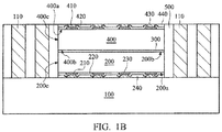
- FIGS. 1A-1E are cross-sectional views of various stages of a method for forming a semiconductor package structure, in accordance with some embodiments of the disclosure. Additional operations can be provided before, during, and/or after the stages described in FIGS. 1A-1E . Some of the stages that are described can be replaced or eliminated for different embodiments. Additional features can be added to the semiconductor package structure. Some of the features described below can be replaced or eliminated for different embodiments. To simplify the diagram, only a portion of the semiconductor package structure is depicted in FIGS. 1A-1E .
- a carrier substrate 100 is provided.
- the carrier substrate 100 is a temporary substrate and will be removed during subsequent steps.
- the carrier substrate 100 is a wafer or a panel.
- the carrier substrate 100 includes glass, silicon, or another suitable carrier material.
- one or more conductive vias 110 are formed on the carrier substrate 100.
- the conductive vias 110 are through package vias (TPVs).
- the conductive vias 110 include copper or another suitable conductive material.
- a semiconductor die 200 is provided on the carrier substrate 100.
- the semiconductor die 200 is flipped and attached to the carrier substrate 100 through an adhesive layer (not shown, which will be removed during subsequent steps).
- multiple semiconductor dies 200 are provided on the carrier substrate 100.
- the semiconductor die 200 is a system-on-chip (SOC), a memory die, an analog processor (AP), a digital processor (DP), a baseband (BB) component, a radio-frequency (RF) component, or another suitable active electronic component.
- the memory die may be a dynamic random access memory (DRAM) die.
- the logic die may be a central processing unit (CPU), a graphics processing unit (GPU), or a DRAM controller.
- the semiconductor die 200 includes an active surface 200a, a non-active surface 200b, and a sidewall 200c. The sidewall 200c may be substantially perpendicular to the active surface 200a and the non-active surface 200b.
- the semiconductor die 200 includes one or more conductive pads 210 at the active surface 200a.
- the conductive pads 210 face the carrier substrate 100.
- the conductive pads 210 may be the topmost layer in an interconnection structure of the semiconductor die 200.
- the conductive pads 210 may be included as a conductive trace of the interconnection structure. To simplify the diagram, only the conductive pads 210 are depicted herein.
- the conductive pads 210 are formed by an electroplating process, a bonding process or another applicable process.
- a passivation layer 220 is disposed at the active surface 200a and partially covers the conductive pads 210.
- the passivation layer 220 includes one or more openings. Each opening exposes a portion of one of the conductive pads 210.
- One or more conductive structures 230 are formed on the passivation layer 220 and fill the openings of the passivation layer 220. As a result, the conductive structures 230 are electrically connected to the conductive pads 210. In some embodiments, the conductive structures 230 are multiple portions of a conductive layer. In some embodiments, the conductive structures 230 are conductive bumps (such as micro bumps), which are balls or pillars. In some other embodiments, the conductive structures 230 are not formed.
- An underfill layer 240 is formed on the passivation layer 220 and surrounds an upper portion of the conductive structures 230. In some other embodiments, the underfill layer 240 is not formed.
- the formation of the semiconductor die 200 includes sequentially forming the conductive pads 210, the passivation layer 220, the conductive structures 230 and the underfill layer 240 on a semiconductor wafer or panel. Afterwards, the semiconductor wafer or panel is diced into multiple semiconductor dies. The semiconductor die 200 is known-good and provided on the carrier substrate 100.
- the semiconductor die 200 is provided on the carrier substrate 100 after the formation of the conductive vias 110. In some other embodiments, the semiconductor die 200 is provided on the carrier substrate 100 before the formation of the conductive vias 110. In some embodiments, the conductive vias 110 are thicker than the semiconductor die 200.
- a semiconductor die 400 is vertically stacked on the semiconductor die 200, in accordance with some embodiments of the disclosure.
- one of the conductive vias 110 and the semiconductor dies 200 and 400 are positioned side by side.
- the conductive vias 110 are thicker than the semiconductor die 400.
- the semiconductor die 400 is attached to the semiconductor die 200 through an adhesive layer 300.
- the adhesive layer 300 is sandwiched between the semiconductor die 200 and the semiconductor die 400.
- multiple semiconductor dies 400 are stacked on the semiconductor die 200.
- the semiconductor die 400 is a SOC, a memory die, an AP, a DP, a BB component, a RF component, or another suitable active electronic component.
- the semiconductor die 400 includes an active surface 400a, a non-active surface 400b, and a sidewall 400c.
- the sidewall 400c may be substantially perpendicular to the active surface 400a and the non-active surface 400b.
- the non-active surface 400b faces the non-active surface 200b.
- the adhesive layer 300 is in direct contact with the non-active surfaces 400b and 200b, and is sandwiched between the non-active surfaces 400b and 200b.
- the semiconductor die 400 includes one or more conductive pads 410 at the active surface 400a.
- the conductive pads 410 face away from the semiconductor die 200 and the carrier substrate 100.
- the conductive pads 210 and 410 face away from each other.
- the conductive pads 410 are formed by an electroplating process, a bonding process or another applicable process.
- the structure and formation of the semiconductor die 400 are similar to or the same as that of the semiconductor die 200. Therefore, the details regarding the passivation layer 420, the conductive structures 430 and the underfill layer 440 are not described again for brevity.
- the semiconductor dies 200 and 400 have different functions.
- one of the semiconductor dies 200 and 400 is a SOC and the other is a memory die.
- one of the semiconductor dies 200 and 400 is an AP and the other is a DP.
- one of the semiconductor dies 200 and 400 is a BB component and the other is a RF component.
- the semiconductor dies 200 and 400 may have the same function.
- the semiconductor dies 200 and 400 are the same size, as shown in FIG. 1B . In some other embodiments, the semiconductor dies 200 and 400 are different sizes. The semiconductor dies 200 and 400 may align or misalign to each other. In some embodiments, the semiconductor die 400 completely vertically overlaps the semiconductor die 200. As a result, the sidewall 400c is substantially coplanar with the sidewall 200c. In some other embodiments, the semiconductor die 400 partially vertically overlaps the semiconductor die 200. As a result, the sidewall 400c is non-coplanar with the sidewall 200c.
- a molding compound 500 is formed on the carrier substrate 100.
- the molding compound 500 surrounds the conductive vias 110, the semiconductor dies 200 and 400, and the adhesive layer 300.
- the molding compound 500 adjoins the sidewalls 200c and 400c.
- a portion of the molding compound 500 is sandwiched between one of the conductive vias 110 and the semiconductor die 200. In some embodiments, a portion of the molding compound 500 is sandwiched between one of the conductive vias 110 and the semiconductor die 400.
- the semiconductor die 400 is narrower than the semiconductor die 200 or the semiconductor dies 200 and 400 do not completely overlap with each other. As a result, a portion of the molding compound 500 extends on the semiconductor die 200. The portion of the molding compound 500 may be in direct contact with the non-active surface 200b. In some embodiments, the semiconductor die 400 is wider than the semiconductor die 200 or the semiconductor dies 200 and 400 do not completely overlap with each other. As a result, a portion of the molding compound 500 extends under the semiconductor die 400. The portion of the molding compound 500 may be in direct contact with the adhesive layer 300.
- the molding compound 500 includes a nonconductive material such as an epoxy, a resin, a moldable polymer, or another suitable molding material.
- the molding compound 500 is applied as a substantial liquid, and then is cured through a chemical reaction.
- the molding compound 500 is an ultraviolet (UV) or thermally cured polymer applied as a gel or malleable solid, and then is cured through a UV or thermal curing process. The molding compound 500 may be cured with a mold.
- the deposited molding compound 500 covers the top surfaces of the conductive vias 110 and the conductive structures 430.
- a thinning process (such as an etching process, a milling process, a grinding process or a polishing process) is performed to thin the deposited molding compound 500.
- the thinned molding compound 500 exposes the top surfaces of the conductive vias 110 and the conductive structures 430.
- the top surface of the molding compound 500 is substantially coplanar with the top surfaces of the conductive vias 110 and the conductive structures 430.
- a redistribution layer (RDL) structure 600 which is also referred to as a fan-out structure, is formed on the molding compound 500, the conductive vias 110, and the semiconductor die 400.
- the RDL structure 600 may include one or more conductive traces disposed in an IMD layer.
- the IMD layer may include multiple sub-dielectric layers successively stacked on the molding compound 500.
- a plurality of conductive traces 620 is positioned on a first sub-dielectric layer 610 and covered by a second sub-dielectric layer 630.
- One of the plurality of conductive traces 620 is electrically coupled to the conductive vias 110 and the semiconductor die 400.
- the conductive pads 410 are electrically connected to the conductive traces 620 of the RDL structure 600 through the conductive structures 430.
- the conductive structures 430 are not formed, and the conductive pads 410 are directly electrically connected to the conductive traces 620. It should be noted that the numbers and the arrangements of the conductive traces and the sub-dielectric layers of the RDL structure 600 shown in the figures are only an example and are not a limitation to the present invention.
- the IMD layer may be formed of organic materials, which include a polymer base material, non-organic materials, which include silicon nitride (SiN x ), silicon oxide (SiO x ), graphene, or the like.
- the first and second sub-dielectric layers 610 and 630 are made of a polymer base material, in which the first sub-dielectric layer 610 has a thickness of about 12 ⁇ m and the second sub-dielectric layer 630 has a thickness of about 24 ⁇ m.
- the IMD layer is a high-k dielectric layer (k is the dielectric constant of the dielectric layer).
- the IMD layer may be formed of a photosensitive material, which includes a dry film photoresist, or a taping film.
- a supporting substrate 700 is provided on the RDL structure 600.
- the supporting substrate 700 is a temporary substrate and will be removed during subsequent steps.
- the supporting substrate 700 includes glass, silicon, or another suitable supportive material.
- the RDL structure 600 is previously formed on the supporting substrate 700. Afterwards, the supporting substrate 700 with the RDL structure 600 is bonded on the molding compound 500, the conductive vias 110, and the semiconductor die 400.
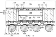
- the carrier substrate 100 is removed.
- an adhesive layer (not shown) may be sandwiched between the semiconductor die 200 and the carrier substrate 100, as aforementioned. After the removal of the carrier substrate 100, this adhesive layer is also removed. For example, a thinning process (such as a grinding process) is performed to remove the adhesive layer.
- the conductive vias 110 and the molding compound 500 may be partially removed during the removal of the adhesive layer.
- a redistribution layer (RDL) structure 800 is formed using the supporting substrate 700 as a carrier.
- the RDL structures 600 and 800 are positioned on two opposite sides of the molding compound 500.
- the semiconductor die 200 is positioned between the RDL structure 800 and the semiconductor die 400, while the semiconductor die 400 is positioned between the RDL structure 600 and the semiconductor die 200.
- the RDL structures 600 and 800 are also positioned on two opposite sides of the conductive vias 110 penetrating the molding compound 500.
- the active surface 200a faces the RDL structure 800 while the active surface 400a faces the RDL structure 600.
- the RDL structure 800 may include one or more conductive traces disposed in an IMD layer.
- the IMD layer may include multiple sub-dielectric layers successively stacked on the molding compound 500.
- a plurality of first conductive traces 820 is positioned on a first sub-dielectric layer 810 and covered by a second sub-dielectric layer 830.
- One of the plurality of first conductive traces 820 is electrically coupled to the conductive vias 110 and the semiconductor die 200.
- the conductive pads 210 are electrically connected to the first conductive traces 820 of the RDL structure 600 through the conductive structures 230. In some other embodiments, the conductive structures 230 are not formed, and the conductive pads 210 are directly electrically connected to the first conductive traces 820.
- a plurality of second conductive traces 840 is positioned on the second sub-dielectric layer 830 and covered by a third sub-dielectric layer 850. It should be noted that the numbers and the arrangements of the conductive traces and the sub-dielectric layers of the RDL structure 800 shown in the figures are only an example and are not a limitation to the present invention.
- Pad portions of conductive traces are exposed from the top of the RDL structure 800.
- the pad portions of the second conductive traces 840 are exposed from openings of the third sub-dielectric layer 850 and connected to subsequently formed conductive components.
- the RDL structure 800 is previously formed on the carrier substrate 100. Subsequently, the conductive vias 110, the semiconductor dies 200 and 400, the molding compound 500, and the RDL structure 600 are formed on the RDL structure 800 on the carrier substrate 100. In this case, the semiconductor die 200 is bonded and electrically connected to the RDL structure 800 through the conductive structures 230. After the supporting substrate 700 is provided on the RDL structure 600, the carrier substrate 100 is removed and the RDL structure 800 is exposed.
- one or more conductive components 900 are formed on the RDL structure 800 using the supporting substrate 700 as a carrier.
- the conductive components 900 are electrically connected to the pad portions of the second conductive traces 840.
- the conductive components 900 are conductive pillars, conductive bumps (such as micro bumps), conductive paste structures, or another suitable conductive component.
- the conductive components 900 may include copper, solder, or another suitable conductive material.
- UBM layer 910 there is an under-bump metallurgy (UBM) layer 910 between one of the conductive components 900 and one pad portion of the second conductive traces 840.
- the UBM layer 910 may include one or more layers, such as a barrier layer and a seed layer.
- the UBM layer 910 including a single layer is depicted herein as an example.
- the supporting substrate 700 is removed.
- the RDL structure 600 is exposed.
- a singulation process is performed after the removal of the supporting substrate 700.
- the RDL structures 600 and 800, and the molding compound 500 may be cut.
- multiple semiconductor packages 1000A are formed.
- the semiconductor package 1000A can be directly bonded onto a printed circuit board (PCB). In this case, there is no semiconductor device (such as a semiconductor die or a semiconductor package) stacked on the semiconductor package 1000A.
- PCB printed circuit board
- each of the semiconductor packages 1000A includes vertically stacked semiconductor dies 200 and 400.
- the non-active surface 200b of the semiconductor die 200 faces the non-active surface 400b of the semiconductor die 400.
- the semiconductor dies 200 and 400 are electrically connected to each other through the overlying RDL structure 600, the underlying RDL structure 800, and the conductive vias 110 by the side thereof.
- multiple semiconductor dies can be integrated in a semiconductor package without increasing the horizontal size (area) of the semiconductor package.
- the length of electrical conduction paths from semiconductor dies to a PCB is short, and there are a large number of the electrical conduction paths. Therefore, a multi-die semiconductor package with a smaller size and better electrical performance is provided.
- FIG. 2 is a cross-sectional view of a semiconductor package structure, in accordance with some embodiments of the disclosure. Elements in FIG. 2 that are the same as those in FIGS. 1A-1E are labeled with the same reference numbers as in FIGS. 1A-1E and are not described again for brevity.
- the structure of the semiconductor package 1000B shown in FIG. 2 is similar to that of the semiconductor package 1000A shown in FIG. IE. The difference between them is that there is a solder mask layer 650 on the RDL structure 600 of the semiconductor package 1000B.
- One or more openings 660 are formed in the solder mask layer 650 and extend into the RDL structure 600 so as to expose pad portions of conductive traces in the RDL structure 600.
- the openings 660 extend into the second sub-dielectric layer 630.
- the pad portions of the conductive traces 620 are exposed from the openings 660.
- solder mask layer 650 and the openings 660 The purpose of the formation of the solder mask layer 650 and the openings 660 is further electrical connection.
- a chip/die may be bonded on the solder mask layer 650 and is electrically connected to the RDL structure 600 through the openings 660.
- a package may be stacked on the semiconductor package 1000B and is electrically connected to the RDL structure 600 through the openings 660.
- the package may be a memory package (such as a DRAM package) or another suitable package.
- a semiconductor package assembly including multiple semiconductor packages can be formed. An example of the semiconductor package assembly will be described in more detail later.
- FIGS. 3 and 4 are cross-sectional views of a semiconductor package structure, in accordance with some embodiments of the disclosure. Elements in FIGS. 3 and 4 that are the same as those in FIGS. 1A-1E and 2 are labeled with the same reference numbers as in FIGS. 1A-1E and 2 and are not described again for brevity.
- the structure of the semiconductor package 1000C shown in FIG. 3 is similar to that of the semiconductor package 1000B shown in FIG. 2 . The difference between them is that there are multiple semiconductor dies 200 and multiple semiconductor dies 400 in the semiconductor package 1000C.
- multiple semiconductor dies 400 are vertically stacked on one semiconductor die 200.
- one semiconductor die 400 is vertically stacked on multiple semiconductor dies 200.
- one of multiple semiconductor dies 400 and one of multiple semiconductor dies 200 do not vertically overlap with each other.
- the semiconductor dies 200 are different sizes.
- the semiconductor dies 200 are the same size.
- the semiconductor dies 400 are different sizes.
- the semiconductor dies 400 are the same size.
- some portions of the molding compound 500 extend between the semiconductor dies 200 and between the semiconductor dies 400, as shown in FIG. 3 .
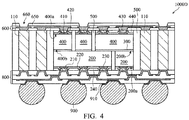
- the structure of the semiconductor package 1000D shown in FIG. 4 is similar to that of the semiconductor packages 1000B and 1000C. The difference between them is that there are multiple semiconductor dies 200 vertically stacked on multiple semiconductor dies 400 in the semiconductor package 1000D.
- the semiconductor dies 200 may be different sizes or the same size.
- the semiconductor dies 400 may be different sizes or the same size.
- some portions of the molding compound 500 extend between the semiconductor dies 200 and between the semiconductor dies 400.
- the semiconductor package 1000B, 1000C, or 1000D includes a solder mask layer 650 with openings 660 on the RDL structure 600
- embodiments of the disclosure are not limited thereto.
- the openings 660, which partially expose the RDL structure 600 are not formed.
- the solder mask layer 650 is not formed on the RDL structure 600. In these cases, there is no semiconductor device (such as a semiconductor die or a semiconductor package) stacked on the semiconductor package 1000B, 1000C, or 1000D.
- the semiconductor package structure and methods for forming the same in accordance with some embodiments of the disclosure provide various advantages.
- Multiple vertically stacked semiconductor dies are integrated in a semiconductor package 1000A, 1000B, 1000C, or 1000D.
- the horizontal size (area) of the semiconductor package 1000A, 1000B, 1000C, or 1000D is much small. Warpage issue can be prevented, too.
- the vertical size (thickness) of the semiconductor package 1000A, 1000B, 1000C, or 1000D is much small. Accordingly, the size of a semiconductor package including multiple semiconductor dies is significantly reduced.
- the formation of the semiconductor package 1000A, 1000B, 1000C, or 1000D is simple and the necessary fabrication cost and time are much less.
- FIG. 5 is a cross-sectional view of a semiconductor package structure, in accordance with some embodiments of the disclosure. Elements in FIG. 5 that are the same as those in FIGS. 1A-1E and 2 are labeled with the same reference numbers as in FIGS. 1A-1E and 2 and are not described again for brevity. It should be noted that the structure of the semiconductor package 2000 shown in FIG. 5 is only an example and is not a limitation to the present invention.
- the semiconductor package 2000 and the semiconductor package 1000B are mounted together and are electrically connected to each other through conductive components 2100.
- the conductive components 2100 are located in the openings 660 and protrude from the solder mask layer 650.
- the conductive components 2100 are conductive bumps (such as micro bumps), conductive pillars, conductive paste structures, or another suitable conductive component.
- the conductive components 2100 may include copper, solder, or another suitable conductive material. In some other embodiments, the conductive components 2100 are surrounded by an underfill material.
- the semiconductor package 2000 comprises a base 2200, at least one semiconductor die (such as two vertically stacked semiconductor dies 2300 and 2400), bonding wires 2500 and a molding compound 2600.
- the base 2200 is a PCB and may be formed of PP or another suitable material.
- the base 2200 is electrically connected to the RDL structure 600 through the conductive components 2100.
- the semiconductor die 2300 is attached on the base 2200 through an adhesive layer such as glue or another suitable adhesive material.
- the semiconductor die 2300 is electrically connected to the base 2200 through its pads 2310 and the bonding wires 2500.
- the semiconductor die 2300 is a memory die or another suitable semiconductor die.
- the semiconductor die 2400 is attached on the semiconductor die 2300 through an adhesive layer such as glue or another suitable adhesive material.
- the semiconductor die 2400 is electrically connected to the base 2200 through its pads 2410 and the bonding wires 2500.
- the semiconductor die 2400 is a memory die or another suitable semiconductor die.
- the semiconductor dies 2300 and 2400 are DRAM dies.
- the pads 2300 and/or 2410 are formed by an electroplating process, a bonding process or another applicable process.
- the molding compound 2600 covers the base 2200 and surrounds the semiconductor dies 2300 and 2400.
- the bonding wires 2500 are embedded in the molding compound 2600.
- the molding compound 2600 is formed of a nonconductive material such as an epoxy, a resin, a moldable polymer, or another suitable molding material.
- the small-sized semiconductor package 1000A and the semiconductor package 2000 are vertically stacked and integrated in the semiconductor package structure/assembly. As a result, a PoP structure including more than two semiconductor dies is provided and its size is greatly reduced.
Landscapes
- Production Of Multi-Layered Print Wiring Board (AREA)
- Structures Or Materials For Encapsulating Or Coating Semiconductor Devices Or Solid State Devices (AREA)
- Engineering & Computer Science (AREA)
- Manufacturing & Machinery (AREA)
- Internal Circuitry In Semiconductor Integrated Circuit Devices (AREA)
Abstract
Description
- This Application claims the benefit of
U.S. Provisional Application No. 62/222,439 filed on September 23, 2015 - The present invention relates to a semiconductor package structure, and in particular to a multi-die semiconductor package structure and methods for forming the same.
- With the continued development of electronics industries, such as those related to the 3Cs (Computer, Communications and Consumer electronics), there has been rapidly increasing consumer demand for devices that are multi-functional, more convenient, and smaller. This demand has driven the need for increased integrated circuit (IC) density. Increased input-output (I/O) pin count and increased demands for IC density have led to the development of multi-die packages. With demands for high performance and high integration, a dual-dies fan-out wafer level chip scale package (WLCSP), through silicon via (TSV) technology and a three-dimensional package on package (3D PoP) structure, have been accepted as some alternative choices.
- However, a dual-dies fan-out WLCSP includes two dies disposed side by side. Accordingly, the size of the package is too big and warpage is an issue of concern. TSV technology comprises forming TSVs penetrating multiple dies. Accordingly, the fabrication cost is high and it wastes the area of the dies. A 3D PoP structure stacks a top package on a bottom package. Accordingly, it is difficult to reduce the thickness of the 3D PoP structure even further.
- Therefore, a novel semiconductor package structure and methods for forming the same are desirable.
- A semiconductor package structure and a method for forming a semiconductor package structure are provided.
- An exemplary embodiment of a semiconductor package structure includes a first semiconductor die including a first active surface and a first non-active surface. The semiconductor package structure also includes a second semiconductor die including a second active surface and a second non-active surface. The second semiconductor die is stacked on the first semiconductor die. The first non-active surface faces the second non-active surface. The semiconductor package structure further includes a first redistribution layer structure. The first active surface faces the first redistribution layer structure. In addition, the semiconductor package structure includes a second redistribution layer structure. The second active surface faces the second redistribution layer structure.
- Another exemplary embodiment of a semiconductor package structure includes a first semiconductor die including a first conductive pad. The semiconductor package structure also includes a second semiconductor die including a second conductive pad. The second semiconductor die vertically overlaps the first semiconductor die. The first and second conductive pads face away from each other. The semiconductor package structure further includes a molding compound surrounding the first semiconductor die and the second semiconductor die.
- An exemplary embodiment of a method for forming a semiconductor package structure includes providing a first semiconductor die including a first non-active surface. The method also includes stacking a second semiconductor die on the first semiconductor die. The first non-active surface faces a second non-active surface of the second semiconductor die. The method further includes forming a molding compound surrounding the first and second semiconductor dies.
- A detailed description is given in the following embodiments with reference to the accompanying drawings.
- The present invention can be more fully understood by reading the subsequent detailed description and examples with references made to the accompanying drawings, wherein:
-
FIGS. 1A-1E are cross-sectional views of various stages of a method for forming a semiconductor package structure, in accordance with some embodiments of the disclosure. -
FIG. 2 is a cross-sectional view of a semiconductor package structure, in accordance with some embodiments of the disclosure. -
FIG. 3 is a cross-sectional view of a semiconductor package structure, in accordance with some embodiments of the disclosure. -
FIG. 4 is a cross-sectional view of a semiconductor package structure, in accordance with some embodiments of the disclosure. -
FIG. 5 is a cross-sectional view of a semiconductor package structure, in accordance with some embodiments of the disclosure. - The following description is of the best-contemplated mode of carrying out the invention. This description is made for the purpose of illustrating the general principles of the invention and should not be taken in a limiting sense. The scope of the invention is determined by reference to the appended claims.
- The present invention will be described with respect to particular embodiments and with reference to certain drawings, but the invention is not limited thereto and is only limited by the claims. The drawings described are only schematic and are non-limiting. In the drawings, the size of some of the elements may be exaggerated for illustrative purposes and not drawn to scale. The dimensions and the relative dimensions may or may not correspond to actual dimensions in the practice of the invention.
-
FIGS. 1A-1E are cross-sectional views of various stages of a method for forming a semiconductor package structure, in accordance with some embodiments of the disclosure. Additional operations can be provided before, during, and/or after the stages described inFIGS. 1A-1E . Some of the stages that are described can be replaced or eliminated for different embodiments. Additional features can be added to the semiconductor package structure. Some of the features described below can be replaced or eliminated for different embodiments. To simplify the diagram, only a portion of the semiconductor package structure is depicted inFIGS. 1A-1E . - As shown in
FIG. 1A , acarrier substrate 100 is provided. Thecarrier substrate 100 is a temporary substrate and will be removed during subsequent steps. In some embodiments, thecarrier substrate 100 is a wafer or a panel. In some embodiments, thecarrier substrate 100 includes glass, silicon, or another suitable carrier material. - As shown in
FIG. 1A , one or moreconductive vias 110 are formed on thecarrier substrate 100. Theconductive vias 110 are through package vias (TPVs). In some embodiments, theconductive vias 110 include copper or another suitable conductive material. - As shown in
FIG. 1A , asemiconductor die 200 is provided on thecarrier substrate 100. In some embodiments, the semiconductor die 200 is flipped and attached to thecarrier substrate 100 through an adhesive layer (not shown, which will be removed during subsequent steps). In some other embodiments, multiple semiconductor dies 200 are provided on thecarrier substrate 100. - In some embodiments, the semiconductor die 200 is a system-on-chip (SOC), a memory die, an analog processor (AP), a digital processor (DP), a baseband (BB) component, a radio-frequency (RF) component, or another suitable active electronic component. The memory die may be a dynamic random access memory (DRAM) die. The logic die may be a central processing unit (CPU), a graphics processing unit (GPU), or a DRAM controller. The semiconductor die 200 includes an
active surface 200a, anon-active surface 200b, and asidewall 200c. Thesidewall 200c may be substantially perpendicular to theactive surface 200a and thenon-active surface 200b. - As shown in
FIG. 1A , the semiconductor die 200 includes one or moreconductive pads 210 at theactive surface 200a. Theconductive pads 210 face thecarrier substrate 100. Theconductive pads 210 may be the topmost layer in an interconnection structure of the semiconductor die 200. In some embodiments, theconductive pads 210 may be included as a conductive trace of the interconnection structure. To simplify the diagram, only theconductive pads 210 are depicted herein. In some embodiments, theconductive pads 210 are formed by an electroplating process, a bonding process or another applicable process. - A
passivation layer 220 is disposed at theactive surface 200a and partially covers theconductive pads 210. Thepassivation layer 220 includes one or more openings. Each opening exposes a portion of one of theconductive pads 210. - One or more
conductive structures 230 are formed on thepassivation layer 220 and fill the openings of thepassivation layer 220. As a result, theconductive structures 230 are electrically connected to theconductive pads 210. In some embodiments, theconductive structures 230 are multiple portions of a conductive layer. In some embodiments, theconductive structures 230 are conductive bumps (such as micro bumps), which are balls or pillars. In some other embodiments, theconductive structures 230 are not formed. - An
underfill layer 240 is formed on thepassivation layer 220 and surrounds an upper portion of theconductive structures 230. In some other embodiments, theunderfill layer 240 is not formed. - In some embodiments, the formation of the semiconductor die 200 includes sequentially forming the
conductive pads 210, thepassivation layer 220, theconductive structures 230 and theunderfill layer 240 on a semiconductor wafer or panel. Afterwards, the semiconductor wafer or panel is diced into multiple semiconductor dies. The semiconductor die 200 is known-good and provided on thecarrier substrate 100. - In some embodiments, the semiconductor die 200 is provided on the
carrier substrate 100 after the formation of theconductive vias 110. In some other embodiments, the semiconductor die 200 is provided on thecarrier substrate 100 before the formation of theconductive vias 110. In some embodiments, theconductive vias 110 are thicker than the semiconductor die 200. - As shown in
FIG. 1B , asemiconductor die 400 is vertically stacked on the semiconductor die 200, in accordance with some embodiments of the disclosure. As a result, one of theconductive vias 110 and the semiconductor dies 200 and 400 are positioned side by side. In some embodiments, theconductive vias 110 are thicker than the semiconductor die 400. - In some embodiments, the semiconductor die 400 is attached to the semiconductor die 200 through an
adhesive layer 300. Theadhesive layer 300 is sandwiched between the semiconductor die 200 and the semiconductor die 400. In some other embodiments, multiple semiconductor dies 400 are stacked on the semiconductor die 200. - In some embodiments, the semiconductor die 400 is a SOC, a memory die, an AP, a DP, a BB component, a RF component, or another suitable active electronic component. The semiconductor die 400 includes an
active surface 400a, anon-active surface 400b, and asidewall 400c. Thesidewall 400c may be substantially perpendicular to theactive surface 400a and thenon-active surface 400b. - In accordance with some embodiments of the disclosure, the
non-active surface 400b faces thenon-active surface 200b. In some embodiments, theadhesive layer 300 is in direct contact with thenon-active surfaces non-active surfaces - As shown in
FIG. 1B , the semiconductor die 400 includes one or moreconductive pads 410 at theactive surface 400a. Theconductive pads 410 face away from the semiconductor die 200 and thecarrier substrate 100. As a result, theconductive pads conductive pads 410 are formed by an electroplating process, a bonding process or another applicable process. In some embodiments, the structure and formation of the semiconductor die 400 are similar to or the same as that of the semiconductor die 200. Therefore, the details regarding thepassivation layer 420, theconductive structures 430 and theunderfill layer 440 are not described again for brevity. - The semiconductor dies 200 and 400 have different functions. For example, in some embodiments, one of the semiconductor dies 200 and 400 is a SOC and the other is a memory die. In some embodiments, one of the semiconductor dies 200 and 400 is an AP and the other is a DP. In some embodiments, one of the semiconductor dies 200 and 400 is a BB component and the other is a RF component. In some other embodiments, the semiconductor dies 200 and 400 may have the same function.
- In some embodiments, the semiconductor dies 200 and 400 are the same size, as shown in
FIG. 1B . In some other embodiments, the semiconductor dies 200 and 400 are different sizes. The semiconductor dies 200 and 400 may align or misalign to each other. In some embodiments, the semiconductor die 400 completely vertically overlaps the semiconductor die 200. As a result, thesidewall 400c is substantially coplanar with thesidewall 200c. In some other embodiments, the semiconductor die 400 partially vertically overlaps the semiconductor die 200. As a result, thesidewall 400c is non-coplanar with thesidewall 200c. - As shown in
FIG. 1B , amolding compound 500 is formed on thecarrier substrate 100. Themolding compound 500 surrounds theconductive vias 110, the semiconductor dies 200 and 400, and theadhesive layer 300. Themolding compound 500 adjoins the sidewalls 200c and 400c. - In some embodiments, a portion of the
molding compound 500 is sandwiched between one of theconductive vias 110 and the semiconductor die 200. In some embodiments, a portion of themolding compound 500 is sandwiched between one of theconductive vias 110 and the semiconductor die 400. - In some embodiments, the semiconductor die 400 is narrower than the semiconductor die 200 or the semiconductor dies 200 and 400 do not completely overlap with each other. As a result, a portion of the
molding compound 500 extends on the semiconductor die 200. The portion of themolding compound 500 may be in direct contact with thenon-active surface 200b. In some embodiments, the semiconductor die 400 is wider than the semiconductor die 200 or the semiconductor dies 200 and 400 do not completely overlap with each other. As a result, a portion of themolding compound 500 extends under the semiconductor die 400. The portion of themolding compound 500 may be in direct contact with theadhesive layer 300. - In some embodiments, the
molding compound 500 includes a nonconductive material such as an epoxy, a resin, a moldable polymer, or another suitable molding material. In some embodiments, themolding compound 500 is applied as a substantial liquid, and then is cured through a chemical reaction. In some other embodiments, themolding compound 500 is an ultraviolet (UV) or thermally cured polymer applied as a gel or malleable solid, and then is cured through a UV or thermal curing process. Themolding compound 500 may be cured with a mold. - In some embodiments, the deposited
molding compound 500 covers the top surfaces of theconductive vias 110 and theconductive structures 430. Afterwards, a thinning process (such as an etching process, a milling process, a grinding process or a polishing process) is performed to thin the depositedmolding compound 500. As a result, the thinnedmolding compound 500 exposes the top surfaces of theconductive vias 110 and theconductive structures 430. In some embodiments, the top surface of themolding compound 500 is substantially coplanar with the top surfaces of theconductive vias 110 and theconductive structures 430. - As shown in
FIG. 1C , a redistribution layer (RDL)structure 600, which is also referred to as a fan-out structure, is formed on themolding compound 500, theconductive vias 110, and the semiconductor die 400. In some embodiments, theRDL structure 600 may include one or more conductive traces disposed in an IMD layer. The IMD layer may include multiple sub-dielectric layers successively stacked on themolding compound 500. - For example, a plurality of
conductive traces 620 is positioned on a firstsub-dielectric layer 610 and covered by a secondsub-dielectric layer 630. One of the plurality ofconductive traces 620 is electrically coupled to theconductive vias 110 and the semiconductor die 400. Theconductive pads 410 are electrically connected to theconductive traces 620 of theRDL structure 600 through theconductive structures 430. In some other embodiments, theconductive structures 430 are not formed, and theconductive pads 410 are directly electrically connected to the conductive traces 620. It should be noted that the numbers and the arrangements of the conductive traces and the sub-dielectric layers of theRDL structure 600 shown in the figures are only an example and are not a limitation to the present invention. - In some embodiments, the IMD layer may be formed of organic materials, which include a polymer base material, non-organic materials, which include silicon nitride (SiNx), silicon oxide (SiOx), graphene, or the like. For example, the first and second
sub-dielectric layers sub-dielectric layer 610 has a thickness of about 12µm and the secondsub-dielectric layer 630 has a thickness of about 24µm. In some embodiments, the IMD layer is a high-k dielectric layer (k is the dielectric constant of the dielectric layer). In some other embodiments, the IMD layer may be formed of a photosensitive material, which includes a dry film photoresist, or a taping film. - As shown in
FIG. 1C , a supportingsubstrate 700 is provided on theRDL structure 600. The supportingsubstrate 700 is a temporary substrate and will be removed during subsequent steps. In some embodiments, the supportingsubstrate 700 includes glass, silicon, or another suitable supportive material. - Embodiments of the disclosure are not limited. In some other embodiments, the
RDL structure 600 is previously formed on the supportingsubstrate 700. Afterwards, the supportingsubstrate 700 with theRDL structure 600 is bonded on themolding compound 500, theconductive vias 110, and the semiconductor die 400. - As shown in FIG. ID, the
carrier substrate 100 is removed. In some embodiments, an adhesive layer (not shown) may be sandwiched between the semiconductor die 200 and thecarrier substrate 100, as aforementioned. After the removal of thecarrier substrate 100, this adhesive layer is also removed. For example, a thinning process (such as a grinding process) is performed to remove the adhesive layer. Theconductive vias 110 and themolding compound 500 may be partially removed during the removal of the adhesive layer. - Afterwards, a redistribution layer (RDL)
structure 800 is formed using the supportingsubstrate 700 as a carrier. TheRDL structures molding compound 500. In other words, the semiconductor die 200 is positioned between theRDL structure 800 and the semiconductor die 400, while the semiconductor die 400 is positioned between theRDL structure 600 and the semiconductor die 200. TheRDL structures conductive vias 110 penetrating themolding compound 500. Theactive surface 200a faces theRDL structure 800 while theactive surface 400a faces theRDL structure 600. - In some embodiments, the
RDL structure 800 may include one or more conductive traces disposed in an IMD layer. The IMD layer may include multiple sub-dielectric layers successively stacked on themolding compound 500. - For example, a plurality of first
conductive traces 820 is positioned on a firstsub-dielectric layer 810 and covered by a secondsub-dielectric layer 830. One of the plurality of firstconductive traces 820 is electrically coupled to theconductive vias 110 and the semiconductor die 200. Theconductive pads 210 are electrically connected to the firstconductive traces 820 of theRDL structure 600 through theconductive structures 230. In some other embodiments, theconductive structures 230 are not formed, and theconductive pads 210 are directly electrically connected to the first conductive traces 820. A plurality of secondconductive traces 840 is positioned on the secondsub-dielectric layer 830 and covered by a thirdsub-dielectric layer 850. It should be noted that the numbers and the arrangements of the conductive traces and the sub-dielectric layers of theRDL structure 800 shown in the figures are only an example and are not a limitation to the present invention. - Pad portions of conductive traces are exposed from the top of the
RDL structure 800. For example, the pad portions of the secondconductive traces 840 are exposed from openings of the thirdsub-dielectric layer 850 and connected to subsequently formed conductive components. - Embodiments of the disclosure are not limited. In some other embodiments, the
RDL structure 800 is previously formed on thecarrier substrate 100. Subsequently, theconductive vias 110, the semiconductor dies 200 and 400, themolding compound 500, and theRDL structure 600 are formed on theRDL structure 800 on thecarrier substrate 100. In this case, the semiconductor die 200 is bonded and electrically connected to theRDL structure 800 through theconductive structures 230. After the supportingsubstrate 700 is provided on theRDL structure 600, thecarrier substrate 100 is removed and theRDL structure 800 is exposed. - As shown in
FIG. 1D , one or moreconductive components 900 are formed on theRDL structure 800 using the supportingsubstrate 700 as a carrier. Theconductive components 900 are electrically connected to the pad portions of the second conductive traces 840. In some embodiments, theconductive components 900 are conductive pillars, conductive bumps (such as micro bumps), conductive paste structures, or another suitable conductive component. Theconductive components 900 may include copper, solder, or another suitable conductive material. - In some embodiments, there is an under-bump metallurgy (UBM)
layer 910 between one of theconductive components 900 and one pad portion of the second conductive traces 840. TheUBM layer 910 may include one or more layers, such as a barrier layer and a seed layer. TheUBM layer 910 including a single layer is depicted herein as an example. - As shown in
FIG. 1E , the supportingsubstrate 700 is removed. As a result, theRDL structure 600 is exposed. In some embodiments, a singulation process is performed after the removal of the supportingsubstrate 700. For example, theRDL structures molding compound 500 may be cut. As a result,multiple semiconductor packages 1000A are formed. In some embodiments, thesemiconductor package 1000A can be directly bonded onto a printed circuit board (PCB). In this case, there is no semiconductor device (such as a semiconductor die or a semiconductor package) stacked on thesemiconductor package 1000A. - As shown in
FIG. 1E , each of thesemiconductor packages 1000A includes vertically stacked semiconductor dies 200 and 400. In particular, thenon-active surface 200b of the semiconductor die 200 faces thenon-active surface 400b of the semiconductor die 400. The semiconductor dies 200 and 400 are electrically connected to each other through the overlyingRDL structure 600, the underlyingRDL structure 800, and theconductive vias 110 by the side thereof. As a result, multiple semiconductor dies can be integrated in a semiconductor package without increasing the horizontal size (area) of the semiconductor package. Moreover, the length of electrical conduction paths from semiconductor dies to a PCB is short, and there are a large number of the electrical conduction paths. Therefore, a multi-die semiconductor package with a smaller size and better electrical performance is provided. - Many variations and/or modifications can be made to embodiments of the disclosure.
FIG. 2 is a cross-sectional view of a semiconductor package structure, in accordance with some embodiments of the disclosure. Elements inFIG. 2 that are the same as those inFIGS. 1A-1E are labeled with the same reference numbers as inFIGS. 1A-1E and are not described again for brevity. - The structure of the
semiconductor package 1000B shown inFIG. 2 is similar to that of thesemiconductor package 1000A shown in FIG. IE. The difference between them is that there is asolder mask layer 650 on theRDL structure 600 of thesemiconductor package 1000B. One ormore openings 660 are formed in thesolder mask layer 650 and extend into theRDL structure 600 so as to expose pad portions of conductive traces in theRDL structure 600. For example, theopenings 660 extend into the secondsub-dielectric layer 630. As a result, the pad portions of theconductive traces 620 are exposed from theopenings 660. - The purpose of the formation of the
solder mask layer 650 and theopenings 660 is further electrical connection. For example, a chip/die may be bonded on thesolder mask layer 650 and is electrically connected to theRDL structure 600 through theopenings 660. Alternatively, a package may be stacked on thesemiconductor package 1000B and is electrically connected to theRDL structure 600 through theopenings 660. For example, the package may be a memory package (such as a DRAM package) or another suitable package. As a result, a semiconductor package assembly including multiple semiconductor packages can be formed. An example of the semiconductor package assembly will be described in more detail later. - Embodiments of the disclosure are not limited to the aforementioned embodiments. More than two semiconductor dies can be integrated in a semiconductor package.
FIGS. 3 and4 are cross-sectional views of a semiconductor package structure, in accordance with some embodiments of the disclosure. Elements inFIGS. 3 and4 that are the same as those inFIGS. 1A-1E and2 are labeled with the same reference numbers as inFIGS. 1A-1E and2 and are not described again for brevity. - The structure of the
semiconductor package 1000C shown inFIG. 3 is similar to that of thesemiconductor package 1000B shown inFIG. 2 . The difference between them is that there are multiple semiconductor dies 200 and multiple semiconductor dies 400 in thesemiconductor package 1000C. - As shown in
FIG. 3 , in some embodiments, multiple semiconductor dies 400 are vertically stacked on one semiconductor die 200. In some embodiments, one semiconductor die 400 is vertically stacked on multiple semiconductor dies 200. In some embodiments, one of multiple semiconductor dies 400 and one of multiple semiconductor dies 200 do not vertically overlap with each other. In some embodiments, the semiconductor dies 200 are different sizes. In some other embodiments, the semiconductor dies 200 are the same size. In some embodiments, the semiconductor dies 400 are different sizes. In some other embodiments, the semiconductor dies 400 are the same size. In some embodiments, some portions of themolding compound 500 extend between the semiconductor dies 200 and between the semiconductor dies 400, as shown inFIG. 3 . - The structure of the
semiconductor package 1000D shown inFIG. 4 is similar to that of thesemiconductor packages semiconductor package 1000D. The semiconductor dies 200 may be different sizes or the same size. The semiconductor dies 400 may be different sizes or the same size. As shown inFIG. 4 , in some embodiments, some portions of themolding compound 500 extend between the semiconductor dies 200 and between the semiconductor dies 400. - Although the
semiconductor package solder mask layer 650 withopenings 660 on theRDL structure 600, embodiments of the disclosure are not limited thereto. In some embodiments, theopenings 660, which partially expose theRDL structure 600, are not formed. In some embodiments, thesolder mask layer 650 is not formed on theRDL structure 600. In these cases, there is no semiconductor device (such as a semiconductor die or a semiconductor package) stacked on thesemiconductor package - The semiconductor package structure and methods for forming the same in accordance with some embodiments of the disclosure provide various advantages. Multiple vertically stacked semiconductor dies are integrated in a
semiconductor package semiconductor package semiconductor package semiconductor package - As mentioned above, various semiconductor packages can be further stacked on the
semiconductor package semiconductor package 2000 is vertically stacked on thesemiconductor package 1000B, as shown inFIG. 5. FIG. 5 is a cross-sectional view of a semiconductor package structure, in accordance with some embodiments of the disclosure. Elements inFIG. 5 that are the same as those inFIGS. 1A-1E and2 are labeled with the same reference numbers as inFIGS. 1A-1E and2 and are not described again for brevity. It should be noted that the structure of thesemiconductor package 2000 shown inFIG. 5 is only an example and is not a limitation to the present invention. - The
semiconductor package 2000 and thesemiconductor package 1000B are mounted together and are electrically connected to each other throughconductive components 2100. Theconductive components 2100 are located in theopenings 660 and protrude from thesolder mask layer 650. In some embodiments, theconductive components 2100 are conductive bumps (such as micro bumps), conductive pillars, conductive paste structures, or another suitable conductive component. Theconductive components 2100 may include copper, solder, or another suitable conductive material. In some other embodiments, theconductive components 2100 are surrounded by an underfill material. - In some embodiments, the
semiconductor package 2000 comprises abase 2200, at least one semiconductor die (such as two vertically stacked semiconductor dies 2300 and 2400), bonding wires 2500 and amolding compound 2600. In some embodiments, thebase 2200 is a PCB and may be formed of PP or another suitable material. Thebase 2200 is electrically connected to theRDL structure 600 through theconductive components 2100. - The semiconductor die 2300 is attached on the
base 2200 through an adhesive layer such as glue or another suitable adhesive material. The semiconductor die 2300 is electrically connected to thebase 2200 through itspads 2310 and the bonding wires 2500. In some embodiments, the semiconductor die 2300 is a memory die or another suitable semiconductor die. The semiconductor die 2400 is attached on the semiconductor die 2300 through an adhesive layer such as glue or another suitable adhesive material. The semiconductor die 2400 is electrically connected to thebase 2200 through itspads 2410 and the bonding wires 2500. In some embodiments, the semiconductor die 2400 is a memory die or another suitable semiconductor die. In some embodiments, the semiconductor dies 2300 and 2400 are DRAM dies. In some embodiments, thepads 2300 and/or 2410 are formed by an electroplating process, a bonding process or another applicable process. - The
molding compound 2600 covers thebase 2200 and surrounds the semiconductor dies 2300 and 2400. The bonding wires 2500 are embedded in themolding compound 2600. In some embodiments, themolding compound 2600 is formed of a nonconductive material such as an epoxy, a resin, a moldable polymer, or another suitable molding material. - As shown in
FIG. 5 , the small-sized semiconductor package 1000A and thesemiconductor package 2000 are vertically stacked and integrated in the semiconductor package structure/assembly. As a result, a PoP structure including more than two semiconductor dies is provided and its size is greatly reduced. - While the invention has been described by way of example and in terms of the preferred embodiments, it should be understood that the invention is not limited to the disclosed embodiments. On the contrary, it is intended to cover various modifications and similar arrangements (as would be apparent to those skilled in the art). Therefore, the scope of the appended claims should be accorded the broadest interpretation so as to encompass all such modifications and similar arrangements.
Claims (15)
- A semiconductor package structure, comprising:a first semiconductor die comprising a first active surface and a first non-active surface;a second semiconductor die comprising a second active surface and a second non-active surface, wherein the second semiconductor die is stacked on the first semiconductor die, and the first non-active surface faces the second non-active surface;a first redistribution layer structure, wherein the first active surface faces the first redistribution layer structure; anda second redistribution layer structure, wherein the second active surface faces the second redistribution layer structure.
- The semiconductor package structure as claimed in claim 1, further comprising an adhesive layer in direct contact with the first non-active surface and the second non-active surface.
- The semiconductor package structure as claimed in claim 1 or 2, further comprising a conductive via disposed around the first and second semiconductor dies,wherein said semiconductor package structure preferably further comprises a molding compound surrounding the conductive via and the first and second semiconductor dies,wherein the first redistribution layer structure and the second redistribution layer structure are preferably located on two opposite sides of the molding compound.
- The semiconductor package structure as claimed in claim one of the preceding claims, wherein a sidewall of the first semiconductor die is substantially coplanar with a sidewall of the second semiconductor die.
- The semiconductor package structure as claimed in one of the preceding claims, wherein the semiconductor package structure comprises a plurality of second semiconductor dies stacked on the first semiconductor die.
- The semiconductor package structure as claimed in one of the preceding claims, wherein the semiconductor package structure comprises a plurality of first semiconductor dies and a plurality of second semiconductor dies, wherein the plurality of second semiconductor dies are stacked on the plurality of first semiconductor dies.
- The semiconductor package structure as claimed in claim 6, further comprising a molding compound between two of the plurality of second semiconductor dies and/or two of the plurality of the first semiconductor dies.
- A semiconductor package structure, comprising:a first semiconductor die comprising a first conductive pad;a second semiconductor die comprising a second conductive pad, wherein the second semiconductor die vertically overlaps the first semiconductor die, and the first andsecond conductive pads face away from each other; anda molding compound surrounding the first semiconductor die and the second semiconductor die.
- The semiconductor package structure as claimed in claim 8, further comprising a conductive via penetrating the molding compound, wherein the first conductive pad is electrically connected to the second conductive pad through the conductive via,wherein a portion of the molding compound is preferably sandwiched between the conductive via and the first or second semiconductor die, and/or wherein the conductive via is preferably thicker than one or both of the first semiconductor die and the second semiconductor die.
- The semiconductor package structure as claimed in claim 8 or 9, further comprising an adhesive layer between the first semiconductor die and the second semiconductor die and surrounded by the molding compound.
- The semiconductor package structure as claimed in one of claims 8 to 10, further comprising a first redistribution layer structure and a second redistribution layer structure positioned on two opposite sides of the molding compound, wherein the first conductive pad faces the first redistribution layer structure and the second conductive pad faces the second redistribution layer structure.
- The semiconductor package structure as claimed in claim 11, further comprising a conductive component connected to the first redistribution layer structure, wherein
the semiconductor package structure preferably further comprises a solder mask layer on the second redistribution layer structure, wherein the solder mask layer comprises an opening exposing a portion of the second redistribution layer structure. - A method for forming a semiconductor package structure, comprising:providing a first semiconductor die comprising a first non-active surface;stacking a second semiconductor die on the first semiconductor die, wherein the first non-active surface faces a second non-active surface of the second semiconductor die; andforming a molding compound surrounding the first and second semiconductor dies.
- The method as claimed in claim 13, further comprising:forming a first redistribution layer structure, wherein the second non-active surface faces the first redistribution layer structure; andforming a second redistribution layer structure, wherein the first non-active surface faces the second redistribution layer structure, and the first and second redistribution layer structures are positioned on two opposite sides of the molding compound,wherein the method preferably further comprises forming a conductive via, wherein the conductive via is disposed around the first and second semiconductor dies.
- The method as claimed in claim 14, wherein the first semiconductor die is provided on a carrier substrate and the conductive via is formed on the carrier substrate, and the method further comprises removing the carrier substrate after the formation of the second redistribution layer structure,wherein said method preferably further comprises:providing a supporting substrate on the second redistribution layer structure before the removal of the carrier substrate; andremoving the supporting substrate after the formation of the first redistribution layer structure, and/orwherein the second non-active surface is attached to the first non-active surface through an adhesive layer.
Applications Claiming Priority (2)
| Application Number | Priority Date | Filing Date | Title |
|---|---|---|---|
| US201562222439P | 2015-09-23 | 2015-09-23 | |
| US15/203,444 US10636773B2 (en) | 2015-09-23 | 2016-07-06 | Semiconductor package structure and method for forming the same |
Publications (2)
| Publication Number | Publication Date |
|---|---|
| EP3157056A2 true EP3157056A2 (en) | 2017-04-19 |
| EP3157056A3 EP3157056A3 (en) | 2017-05-10 |
Family
ID=58283209
Family Applications (1)
| Application Number | Title | Priority Date | Filing Date |
|---|---|---|---|
| EP16183501.2A Ceased EP3157056A3 (en) | 2015-09-23 | 2016-08-10 | Semiconductor package structure and method for forming the same |
Country Status (4)
| Country | Link |
|---|---|
| US (1) | US10636773B2 (en) |
| EP (1) | EP3157056A3 (en) |
| CN (1) | CN106558573A (en) |
| TW (1) | TWI587467B (en) |
Cited By (5)
| Publication number | Priority date | Publication date | Assignee | Title |
|---|---|---|---|---|
| TWI688059B (en) * | 2019-03-14 | 2020-03-11 | 力成科技股份有限公司 | Semiconductor package structure and manufacturing method thereof |
| TWI713162B (en) * | 2018-09-14 | 2020-12-11 | 聯發科技股份有限公司 | A semiconductor package structure and method of forming the same |
| US11854784B2 (en) | 2018-09-14 | 2023-12-26 | Mediatek Inc. | Chip scale package structure and method of forming the same |
| EP4383325A1 (en) * | 2022-12-06 | 2024-06-12 | NXP USA, Inc. | Double-sided multichip packages |
| US12628685B2 (en) | 2023-08-30 | 2026-05-12 | Nxp Usa, Inc. | Double-sided multichip packages with direct die-to-die coupling |
Families Citing this family (72)
| Publication number | Priority date | Publication date | Assignee | Title |
|---|---|---|---|---|
| US10535633B2 (en) | 2015-07-02 | 2020-01-14 | Taiwan Semiconductor Manufacturing Company, Ltd. | Chip package having die structures of different heights and method of forming same |
| US9960150B2 (en) * | 2016-06-13 | 2018-05-01 | Micron Technology, Inc. | Semiconductor device assembly with through-mold cooling channel formed in encapsulant |
| US9859253B1 (en) * | 2016-06-29 | 2018-01-02 | Intel Corporation | Integrated circuit package stack |
| US10290590B2 (en) * | 2016-11-29 | 2019-05-14 | Taiwan Semiconductor Manufacturing Company Ltd. | Stacked semiconductor device and method of manufacturing the same |
| WO2018112914A1 (en) * | 2016-12-23 | 2018-06-28 | Intel Corporation | Vertical bond- wire stacked chip-scale package with application-specific integrated circuit die on stack, and methods of making same |
| TWI643305B (en) * | 2017-01-16 | 2018-12-01 | Powertech Technology Inc. | Package structure and manufacturing method thereof |
| US10403602B2 (en) * | 2017-06-29 | 2019-09-03 | Intel IP Corporation | Monolithic silicon bridge stack including a hybrid baseband die supporting processors and memory |
| US10872885B2 (en) * | 2017-06-30 | 2020-12-22 | Taiwan Semiconductor Manufacturing Company, Ltd. | Integrated circuit packages and methods of forming same |
| DE102018108409B4 (en) | 2017-06-30 | 2023-08-10 | Taiwan Semiconductor Manufacturing Co., Ltd. | INTEGRATED CIRCUIT PACKAGES AND METHOD OF MAKING THEM |
| US10290611B2 (en) | 2017-07-27 | 2019-05-14 | Taiwan Semiconductor Manufacturing Company, Ltd. | Semiconductor packages and methods of forming same |
| US10475747B2 (en) * | 2017-08-14 | 2019-11-12 | Taiwan Semiconductor Manufacturing Co., Ltd. | Integrated fan-out package and method for fabricating the same |
| US10636757B2 (en) * | 2017-08-29 | 2020-04-28 | Taiwan Semiconductor Manufacturing Co., Ltd. | Integrated circuit component package and method of fabricating the same |
| CN107579009A (en) * | 2017-09-02 | 2018-01-12 | 中国电子科技集团公司第五十八研究所 | A kind of multi-chip laminated packaging structure and preparation method thereof |
| CN107731761A (en) * | 2017-09-30 | 2018-02-23 | 睿力集成电路有限公司 | Base semiconductor packaging part and its manufacture method |
| CN109671680A (en) * | 2017-10-16 | 2019-04-23 | 台湾积体电路制造股份有限公司 | The chip packaging piece of tube core structure and forming method thereof with different height |
| TWI736780B (en) | 2017-10-31 | 2021-08-21 | 台灣積體電路製造股份有限公司 | Chip package and methods of forming the same |
| US11322449B2 (en) | 2017-10-31 | 2022-05-03 | Taiwan Semiconductor Manufacturing Co., Ltd. | Package with fan-out structures |
| DE102018122228B4 (en) | 2017-11-15 | 2023-01-26 | Taiwan Semiconductor Manufacturing Company, Ltd. | Integrated multichip fan-out package and method for its manufacture |
| US10515922B2 (en) | 2017-11-15 | 2019-12-24 | Taiwan Semiconductor Manufacturing Company, Ltd. | Multi-chip integrated fan-out package |
| US11232957B2 (en) * | 2017-11-29 | 2022-01-25 | Pep Inovation Pte. Ltd. | Chip packaging method and package structure |
| US12506055B2 (en) | 2017-11-29 | 2025-12-23 | Pep Innovation Pte. Ltd. | Chip packaging method and chip structure |
| US11610855B2 (en) * | 2017-11-29 | 2023-03-21 | Pep Innovation Pte. Ltd. | Chip packaging method and package structure |
| US20190247618A1 (en) * | 2018-02-09 | 2019-08-15 | Qualcomm Incorporated | Wireless guidewire |
| US11075151B2 (en) | 2018-06-29 | 2021-07-27 | Taiwan Semiconductor Manufacturing Company, Ltd. | Fan-out package with controllable standoff |
| US10510668B1 (en) * | 2018-07-16 | 2019-12-17 | Taiwan Semiconductor Manufacturing Co., Ltd. | Method of fabricating semiconductor device |
| EP3621104A1 (en) | 2018-09-05 | 2020-03-11 | Infineon Technologies Austria AG | Semiconductor package and method of manufacturing a semiconductor package |
| TWI679735B (en) * | 2018-10-05 | 2019-12-11 | 力成科技股份有限公司 | Double-sided fan-out package on package (pop) and packaging method thereof |
| CN109638009A (en) * | 2018-12-17 | 2019-04-16 | 华进半导体封装先导技术研发中心有限公司 | A kind of Multi-chip laminating fan-out package structure and its manufacturing method |
| US20200203470A1 (en) * | 2018-12-20 | 2020-06-25 | Intel Corporation | Magnetic mold material inductors for electronic packages |
| US10770433B1 (en) * | 2019-02-27 | 2020-09-08 | Apple Inc. | High bandwidth die to die interconnect with package area reduction |
| CN210006733U (en) * | 2019-03-04 | 2020-01-31 | Pep创新私人有限公司 | Chip packaging structure |
| US11657862B2 (en) * | 2019-03-22 | 2023-05-23 | Intel Corporation | Electrically coupled trace routing configuration in multiple layers |
| US11600590B2 (en) * | 2019-03-22 | 2023-03-07 | Advanced Semiconductor Engineering, Inc. | Semiconductor device and semiconductor package |
| US10867966B2 (en) * | 2019-04-29 | 2020-12-15 | Taiwan Semiconductor Manufacturing Company, Ltd. | Package structure, package-on-package structure and method of fabricating the same |
| KR102671078B1 (en) * | 2019-05-02 | 2024-05-30 | 에스케이하이닉스 주식회사 | Stack package including fan out sub package |
| US11133423B2 (en) * | 2019-07-03 | 2021-09-28 | Advanced Semiconductor Engineering, Inc. | Optical device and method of manufacturing the same |
| CN110634838A (en) * | 2019-08-29 | 2019-12-31 | 上海先方半导体有限公司 | An ultra-thin fan-out package structure and manufacturing method thereof |
| US11856800B2 (en) * | 2019-09-20 | 2023-12-26 | Taiwan Semiconductor Manufacturing Company, Ltd. | Semiconductor devices with system on chip devices |
| DE102020106799A1 (en) | 2019-09-20 | 2021-03-25 | Taiwan Semiconductor Manufacturing Co., Ltd. | SEMICONDUCTOR COMPONENTS AND METHOD OF MANUFACTURING |
| US11251100B2 (en) * | 2019-09-25 | 2022-02-15 | Taiwan Semiconductor Manufacturing Company, Ltd. | Semiconductor structure having an anti-arcing pattern disposed on a passivation layer and method of fabricating the semiconductor structure |
| CN112687613A (en) * | 2019-10-17 | 2021-04-20 | 美光科技公司 | Microelectronic device assembly and package including surface mount components |
| CN112687615B (en) | 2019-10-17 | 2025-03-07 | 美光科技公司 | Microelectronic device assembly, package and related methods |
| US12199068B2 (en) * | 2019-10-17 | 2025-01-14 | Micron Technology, Inc. | Methods of forming microelectronic device assemblies and packages |
| CN112687614B (en) | 2019-10-17 | 2024-11-26 | 美光科技公司 | Microelectronic device assembly and package including multiple device stacks and related methods |
| US11410973B2 (en) * | 2019-10-17 | 2022-08-09 | Micron Technology, Inc. | Microelectronic device assemblies and packages and related methods and systems |
| US11502024B2 (en) * | 2020-01-21 | 2022-11-15 | Advanced Semiconductor Engineering, Inc. | Semiconductor device package and method of manufacturing the same |
| TWI751506B (en) * | 2020-03-06 | 2022-01-01 | 欣興電子股份有限公司 | Wiring board and manufacturing method thereof |
| CN111370395B (en) * | 2020-03-24 | 2022-12-23 | 青岛歌尔智能传感器有限公司 | Packaging structure, packaging method and wearable device of heart rate module |
| DE102021107982B4 (en) | 2020-04-07 | 2024-02-22 | Mediatek Inc. | SEMICONDUCTOR PACKAGE STRUCTURE |
| US11830851B2 (en) * | 2020-04-07 | 2023-11-28 | Mediatek Inc. | Semiconductor package structure |
| US11710702B2 (en) | 2020-06-08 | 2023-07-25 | Micron Technology, Inc. | Substrate-free semiconductor device assemblies with multiple semiconductor devices and methods for making the same |
| KR102877010B1 (en) * | 2020-06-09 | 2025-10-28 | 삼성전자주식회사 | Semiconductor package |
| US11456291B2 (en) * | 2020-06-24 | 2022-09-27 | Qualcomm Incorporated | Integrated circuit (IC) packages employing split, double-sided metallization structures to facilitate a semiconductor die (“die”) module employing stacked dice, and related fabrication methods |
| US11688681B2 (en) * | 2020-08-24 | 2023-06-27 | Ap Memory Technology Corporation | DRAM chiplet structure and method for manufacturing the same |
| KR102822679B1 (en) * | 2020-10-08 | 2025-06-20 | 삼성전자주식회사 | Semiconductor pacakge device |
| CN114446798A (en) * | 2020-11-04 | 2022-05-06 | 矽磐微电子(重庆)有限公司 | Semiconductor packaging method and semiconductor packaging structure |
| US11450645B2 (en) * | 2020-11-24 | 2022-09-20 | Micron Technology, Inc. | Semiconductor assemblies with hybrid fanouts and associated methods and systems |
| US11923285B2 (en) * | 2021-01-05 | 2024-03-05 | Advanced Semiconductor Engineering, Inc. | Electronic device package and method of manufacturing the same |
| CN112908868A (en) * | 2021-01-18 | 2021-06-04 | 上海先方半导体有限公司 | Three-dimensional packaging method and structure of memory |
| WO2023010555A1 (en) * | 2021-08-06 | 2023-02-09 | 华为技术有限公司 | Chip package structure and electronic device |
| KR102958274B1 (en) | 2021-08-18 | 2026-04-29 | 삼성전자주식회사 | Semiconductor package |
| US12230622B2 (en) * | 2021-10-13 | 2025-02-18 | Mediatek Inc. | Electronic device with stacked printed circuit boards |
| CN114093861B (en) * | 2021-11-19 | 2023-12-22 | 盛合晶微半导体(江阴)有限公司 | Three-dimensional fan-out integrated packaging structure and packaging method and wireless earphones |
| KR102899653B1 (en) | 2021-12-10 | 2025-12-11 | 삼성전자 주식회사 | Fan-Out Semiconductor Package |
| US12153268B2 (en) * | 2022-01-03 | 2024-11-26 | Apple Inc. | Technologies for increased volumetric and functional efficiencies of optical packages |
| US12315853B2 (en) * | 2022-01-24 | 2025-05-27 | Apple Inc. | System packaging for cellular modem and transceiver system of heterogeneous stacking |
| US12588522B2 (en) | 2022-07-11 | 2026-03-24 | Mediatek Inc. | Semiconductor package structure |
| CN115425020B (en) * | 2022-09-16 | 2025-07-25 | 上海为旌科技有限公司 | Multi-chip package interconnection structure, manufacturing method and electronic equipment |
| KR102929756B1 (en) * | 2022-11-24 | 2026-02-20 | 양쯔 메모리 테크놀로지스 씨오., 엘티디. | Memory system package structure and manufacturing method thereof |
| KR20240080228A (en) * | 2022-11-28 | 2024-06-07 | 삼성전자주식회사 | Semiconductor package and method for manufacturing the same |
| CN115547852B (en) * | 2022-12-01 | 2023-03-07 | 合肥矽迈微电子科技有限公司 | Semi-finished product structure of high-power chip, device and packaging process of device |
| KR20240113671A (en) * | 2023-01-13 | 2024-07-23 | 삼성전자주식회사 | Semiconductor package |
Citations (2)
| Publication number | Priority date | Publication date | Assignee | Title |
|---|---|---|---|---|
| US20090127686A1 (en) * | 2007-11-21 | 2009-05-21 | Advanced Chip Engineering Technology Inc. | Stacking die package structure for semiconductor devices and method of the same |
| US8729714B1 (en) * | 2012-12-31 | 2014-05-20 | Intel Mobile Communications GmbH | Flip-chip wafer level package and methods thereof |
Family Cites Families (14)
| Publication number | Priority date | Publication date | Assignee | Title |
|---|---|---|---|---|
| US7166495B2 (en) * | 1996-02-20 | 2007-01-23 | Micron Technology, Inc. | Method of fabricating a multi-die semiconductor package assembly |
| JP3481444B2 (en) * | 1998-01-14 | 2003-12-22 | シャープ株式会社 | Semiconductor device and manufacturing method thereof |
| US6093969A (en) * | 1999-05-15 | 2000-07-25 | Lin; Paul T. | Face-to-face (FTF) stacked assembly of substrate-on-bare-chip (SOBC) modules |
| JP3581086B2 (en) * | 2000-09-07 | 2004-10-27 | 松下電器産業株式会社 | Semiconductor device |
| TW511415B (en) * | 2001-01-19 | 2002-11-21 | Matsushita Electric Industrial Co Ltd | Component built-in module and its manufacturing method |
| SG121705A1 (en) * | 2002-02-21 | 2006-05-26 | United Test & Assembly Ct Ltd | Semiconductor package |
| WO2007126090A1 (en) | 2006-04-27 | 2007-11-08 | Nec Corporation | Circuit board, electronic device and method for manufacturing circuit board |
| US20080079150A1 (en) * | 2006-09-28 | 2008-04-03 | Juergen Simon | Die arrangement and method for producing a die arrangement |
| KR101501739B1 (en) | 2008-03-21 | 2015-03-11 | 삼성전자주식회사 | Method of Fabricating Semiconductor Packages |
| US20100193930A1 (en) * | 2009-02-02 | 2010-08-05 | Samsung Electronics Co., Ltd. | Multi-chip semiconductor devices having conductive vias and methods of forming the same |
| US7923304B2 (en) * | 2009-09-10 | 2011-04-12 | Stats Chippac Ltd. | Integrated circuit packaging system with conductive pillars and method of manufacture thereof |
| US8518746B2 (en) | 2010-09-02 | 2013-08-27 | Stats Chippac, Ltd. | Semiconductor device and method of forming TSV semiconductor wafer with embedded semiconductor die |
| CN103296014A (en) | 2012-02-28 | 2013-09-11 | 刘胜 | Fan-out wafer level semiconductor chip three-dimensional stacking packaging structure and technology |
| US8975726B2 (en) | 2012-10-11 | 2015-03-10 | Taiwan Semiconductor Manufacturing Company, Ltd. | POP structures and methods of forming the same |
-
2016
- 2016-07-06 US US15/203,444 patent/US10636773B2/en active Active
- 2016-08-04 CN CN201610635402.8A patent/CN106558573A/en not_active Withdrawn
- 2016-08-10 EP EP16183501.2A patent/EP3157056A3/en not_active Ceased
- 2016-08-17 TW TW105126198A patent/TWI587467B/en not_active IP Right Cessation
Patent Citations (2)
| Publication number | Priority date | Publication date | Assignee | Title |
|---|---|---|---|---|
| US20090127686A1 (en) * | 2007-11-21 | 2009-05-21 | Advanced Chip Engineering Technology Inc. | Stacking die package structure for semiconductor devices and method of the same |
| US8729714B1 (en) * | 2012-12-31 | 2014-05-20 | Intel Mobile Communications GmbH | Flip-chip wafer level package and methods thereof |
Cited By (8)
| Publication number | Priority date | Publication date | Assignee | Title |
|---|---|---|---|---|
| TWI713162B (en) * | 2018-09-14 | 2020-12-11 | 聯發科技股份有限公司 | A semiconductor package structure and method of forming the same |
| US11450606B2 (en) | 2018-09-14 | 2022-09-20 | Mediatek Inc. | Chip scale package structure and method of forming the same |
| US11791266B2 (en) | 2018-09-14 | 2023-10-17 | Mediatek Inc. | Chip scale package structure and method of forming the same |
| US11854784B2 (en) | 2018-09-14 | 2023-12-26 | Mediatek Inc. | Chip scale package structure and method of forming the same |
| TWI688059B (en) * | 2019-03-14 | 2020-03-11 | 力成科技股份有限公司 | Semiconductor package structure and manufacturing method thereof |
| EP4383325A1 (en) * | 2022-12-06 | 2024-06-12 | NXP USA, Inc. | Double-sided multichip packages |
| US12538844B2 (en) | 2022-12-06 | 2026-01-27 | Nxp Usa, Inc. | Double-sided multichip packages |
| US12628685B2 (en) | 2023-08-30 | 2026-05-12 | Nxp Usa, Inc. | Double-sided multichip packages with direct die-to-die coupling |
Also Published As
| Publication number | Publication date |
|---|---|
| TWI587467B (en) | 2017-06-11 |
| CN106558573A (en) | 2017-04-05 |
| US10636773B2 (en) | 2020-04-28 |
| TW201712828A (en) | 2017-04-01 |
| US20170084589A1 (en) | 2017-03-23 |
| EP3157056A3 (en) | 2017-05-10 |
Similar Documents
| Publication | Publication Date | Title |
|---|---|---|
| US10636773B2 (en) | Semiconductor package structure and method for forming the same | |
| US20230378078A1 (en) | Package with fan-out structures | |
| US11764159B2 (en) | Package with fan-out structures | |
| KR102318303B1 (en) | Die stacks and methods forming same | |
| CN106952831B (en) | Device using thermally and mechanically strengthened layers and method of making same | |
| US20200328183A1 (en) | Discrete Polymer in Fan-Out Packages | |
| EP3096349A1 (en) | Semiconductor package assembly and method for forming the same | |
| US20260076206A1 (en) | Package structure with a plurality of corner openings comprising different shapes | |
| US12237262B2 (en) | Semiconductor package with improved interposer structure | |
| EP3154085A1 (en) | Semiconductor package structure and method for forming the same | |
| EP3096350A1 (en) | Semiconductor package assembly and method for forming the same | |
| US10504810B2 (en) | Polymer-based-semiconductor structure with cavity | |
| CN106206509B (en) | Electronic package and its manufacturing method and substrate structure | |
| US10096541B2 (en) | Method for fabricating electronic package | |
| CN106252324A (en) | Package-on-package stacked package structure | |
| US9875949B2 (en) | Electronic package having circuit structure with plurality of metal layers, and fabrication method thereof | |
| CN103871991A (en) | Methods and Apparatus for Package with Interposers | |
| US11631630B2 (en) | Pillar-last methods for forming semiconductor devices | |
| CN221102061U (en) | Package | |
| CN115763448A (en) | Semiconductor package and method of manufacturing the same | |
| US11201142B2 (en) | Semiconductor package, package on package structure and method of froming package on package structure | |
| US10790210B2 (en) | Semiconductor package and manufacturing method thereof | |
| US12557698B2 (en) | Package and manufacturing method thereof | |
| CN121312324A (en) | Edge recess design for molded and melt-bonded or hybrid-bonded integrated circuits |
Legal Events
| Date | Code | Title | Description |
|---|---|---|---|
| PUAI | Public reference made under article 153(3) epc to a published international application that has entered the european phase |
Free format text: ORIGINAL CODE: 0009012 |
|
| STAA | Information on the status of an ep patent application or granted ep patent |
Free format text: STATUS: THE APPLICATION HAS BEEN PUBLISHED |
|
| PUAL | Search report despatched |
Free format text: ORIGINAL CODE: 0009013 |
|
| AK | Designated contracting states |
Kind code of ref document: A2 Designated state(s): AL AT BE BG CH CY CZ DE DK EE ES FI FR GB GR HR HU IE IS IT LI LT LU LV MC MK MT NL NO PL PT RO RS SE SI SK SM TR |
|
| AX | Request for extension of the european patent |
Extension state: BA ME |
|
| AK | Designated contracting states |
Kind code of ref document: A3 Designated state(s): AL AT BE BG CH CY CZ DE DK EE ES FI FR GB GR HR HU IE IS IT LI LT LU LV MC MK MT NL NO PL PT RO RS SE SI SK SM TR |
|
| AX | Request for extension of the european patent |
Extension state: BA ME |
|
| RIC1 | Information provided on ipc code assigned before grant |
Ipc: H01L 23/538 20060101AFI20170406BHEP Ipc: H01L 23/31 20060101ALN20170406BHEP Ipc: H01L 21/56 20060101ALN20170406BHEP Ipc: H01L 25/065 20060101ALN20170406BHEP Ipc: H01L 25/10 20060101ALI20170406BHEP |
|
| STAA | Information on the status of an ep patent application or granted ep patent |
Free format text: STATUS: REQUEST FOR EXAMINATION WAS MADE |
|
| 17P | Request for examination filed |
Effective date: 20171027 |
|
| RBV | Designated contracting states (corrected) |
Designated state(s): AL AT BE BG CH CY CZ DE DK EE ES FI FR GB GR HR HU IE IS IT LI LT LU LV MC MK MT NL NO PL PT RO RS SE SI SK SM TR |
|
| STAA | Information on the status of an ep patent application or granted ep patent |
Free format text: STATUS: EXAMINATION IS IN PROGRESS |
|
| 17Q | First examination report despatched |
Effective date: 20191028 |
|
| STAA | Information on the status of an ep patent application or granted ep patent |
Free format text: STATUS: THE APPLICATION HAS BEEN REFUSED |
|
| 18R | Application refused |
Effective date: 20210124 |
|
| P01 | Opt-out of the competence of the unified patent court (upc) registered |
Effective date: 20230607 |