EP3147954A1 - Photodetector with conductive channel made from two dimensional material and its manufacturing method - Google Patents
Photodetector with conductive channel made from two dimensional material and its manufacturing method Download PDFInfo
- Publication number
- EP3147954A1 EP3147954A1 EP15186234.9A EP15186234A EP3147954A1 EP 3147954 A1 EP3147954 A1 EP 3147954A1 EP 15186234 A EP15186234 A EP 15186234A EP 3147954 A1 EP3147954 A1 EP 3147954A1
- Authority
- EP
- European Patent Office
- Prior art keywords
- conductive channel
- layer
- dimensional conductive
- quantum dot
- textured
- Prior art date
- Legal status (The legal status is an assumption and is not a legal conclusion. Google has not performed a legal analysis and makes no representation as to the accuracy of the status listed.)
- Withdrawn
Links
Images


Classifications
-
- H—ELECTRICITY
- H10—SEMICONDUCTOR DEVICES; ELECTRIC SOLID-STATE DEVICES NOT OTHERWISE PROVIDED FOR
- H10F—INORGANIC SEMICONDUCTOR DEVICES SENSITIVE TO INFRARED RADIATION, LIGHT, ELECTROMAGNETIC RADIATION OF SHORTER WAVELENGTH OR CORPUSCULAR RADIATION
- H10F77/00—Constructional details of devices covered by this subclass
- H10F77/10—Semiconductor bodies
- H10F77/12—Active materials
- H10F77/122—Active materials comprising only Group IV materials
-
- H—ELECTRICITY
- H10—SEMICONDUCTOR DEVICES; ELECTRIC SOLID-STATE DEVICES NOT OTHERWISE PROVIDED FOR
- H10F—INORGANIC SEMICONDUCTOR DEVICES SENSITIVE TO INFRARED RADIATION, LIGHT, ELECTROMAGNETIC RADIATION OF SHORTER WAVELENGTH OR CORPUSCULAR RADIATION
- H10F30/00—Individual radiation-sensitive semiconductor devices in which radiation controls the flow of current through the devices, e.g. photodetectors
- H10F30/20—Individual radiation-sensitive semiconductor devices in which radiation controls the flow of current through the devices, e.g. photodetectors the devices having potential barriers, e.g. phototransistors
- H10F30/21—Individual radiation-sensitive semiconductor devices in which radiation controls the flow of current through the devices, e.g. photodetectors the devices having potential barriers, e.g. phototransistors the devices being sensitive to infrared, visible or ultraviolet radiation
- H10F30/28—Individual radiation-sensitive semiconductor devices in which radiation controls the flow of current through the devices, e.g. photodetectors the devices having potential barriers, e.g. phototransistors the devices being sensitive to infrared, visible or ultraviolet radiation the devices being characterised by field-effect operation, e.g. junction field-effect phototransistors
-
- H—ELECTRICITY
- H10—SEMICONDUCTOR DEVICES; ELECTRIC SOLID-STATE DEVICES NOT OTHERWISE PROVIDED FOR
- H10F—INORGANIC SEMICONDUCTOR DEVICES SENSITIVE TO INFRARED RADIATION, LIGHT, ELECTROMAGNETIC RADIATION OF SHORTER WAVELENGTH OR CORPUSCULAR RADIATION
- H10F71/00—Manufacture or treatment of devices covered by this subclass
-
- H—ELECTRICITY
- H10—SEMICONDUCTOR DEVICES; ELECTRIC SOLID-STATE DEVICES NOT OTHERWISE PROVIDED FOR
- H10F—INORGANIC SEMICONDUCTOR DEVICES SENSITIVE TO INFRARED RADIATION, LIGHT, ELECTROMAGNETIC RADIATION OF SHORTER WAVELENGTH OR CORPUSCULAR RADIATION
- H10F77/00—Constructional details of devices covered by this subclass
- H10F77/10—Semiconductor bodies
- H10F77/14—Shape of semiconductor bodies; Shapes, relative sizes or dispositions of semiconductor regions within semiconductor bodies
- H10F77/143—Shape of semiconductor bodies; Shapes, relative sizes or dispositions of semiconductor regions within semiconductor bodies comprising quantum structures
-
- H—ELECTRICITY
- H10—SEMICONDUCTOR DEVICES; ELECTRIC SOLID-STATE DEVICES NOT OTHERWISE PROVIDED FOR
- H10F—INORGANIC SEMICONDUCTOR DEVICES SENSITIVE TO INFRARED RADIATION, LIGHT, ELECTROMAGNETIC RADIATION OF SHORTER WAVELENGTH OR CORPUSCULAR RADIATION
- H10F77/00—Constructional details of devices covered by this subclass
- H10F77/10—Semiconductor bodies
- H10F77/14—Shape of semiconductor bodies; Shapes, relative sizes or dispositions of semiconductor regions within semiconductor bodies
- H10F77/143—Shape of semiconductor bodies; Shapes, relative sizes or dispositions of semiconductor regions within semiconductor bodies comprising quantum structures
- H10F77/1433—Quantum dots
-
- H—ELECTRICITY
- H10—SEMICONDUCTOR DEVICES; ELECTRIC SOLID-STATE DEVICES NOT OTHERWISE PROVIDED FOR
- H10F—INORGANIC SEMICONDUCTOR DEVICES SENSITIVE TO INFRARED RADIATION, LIGHT, ELECTROMAGNETIC RADIATION OF SHORTER WAVELENGTH OR CORPUSCULAR RADIATION
- H10F77/00—Constructional details of devices covered by this subclass
- H10F77/70—Surface textures, e.g. pyramid structures
- H10F77/703—Surface textures, e.g. pyramid structures of the semiconductor bodies, e.g. textured active layers
-
- H—ELECTRICITY
- H10—SEMICONDUCTOR DEVICES; ELECTRIC SOLID-STATE DEVICES NOT OTHERWISE PROVIDED FOR
- H10F—INORGANIC SEMICONDUCTOR DEVICES SENSITIVE TO INFRARED RADIATION, LIGHT, ELECTROMAGNETIC RADIATION OF SHORTER WAVELENGTH OR CORPUSCULAR RADIATION
- H10F77/00—Constructional details of devices covered by this subclass
- H10F77/70—Surface textures, e.g. pyramid structures
- H10F77/707—Surface textures, e.g. pyramid structures of the substrates or of layers on substrates, e.g. textured ITO layer on a glass substrate
-
- Y—GENERAL TAGGING OF NEW TECHNOLOGICAL DEVELOPMENTS; GENERAL TAGGING OF CROSS-SECTIONAL TECHNOLOGIES SPANNING OVER SEVERAL SECTIONS OF THE IPC; TECHNICAL SUBJECTS COVERED BY FORMER USPC CROSS-REFERENCE ART COLLECTIONS [XRACs] AND DIGESTS
- Y02—TECHNOLOGIES OR APPLICATIONS FOR MITIGATION OR ADAPTATION AGAINST CLIMATE CHANGE
- Y02E—REDUCTION OF GREENHOUSE GAS [GHG] EMISSIONS, RELATED TO ENERGY GENERATION, TRANSMISSION OR DISTRIBUTION
- Y02E10/00—Energy generation through renewable energy sources
- Y02E10/50—Photovoltaic [PV] energy
- Y02E10/547—Monocrystalline silicon PV cells
Definitions
- the present disclosure relates to the field of two-dimensional materials and electronic devices such as photodetectors and field effect transistors (FETs) comprising two-dimensional materials.
- electronic devices such as photodetectors and field effect transistors (FETs) comprising two-dimensional materials.
- Certain aspects/embodiments may relate to sensing (e.g. optical sensing) and imaging for healthcare, automotive or wearable applications.
- Other disclosed example aspects/embodiments relate to portable electronic devices, in particular, so-called hand-portable electronic devices which may be hand-held in use (although they may be placed in a cradle in use).
- hand-portable electronic devices include so-called Personal Digital Assistants (PDAs) and tablet PCs.
- the portable electronic devices/apparatus may provide one or more audio/text/video communication functions (e.g. tele-communication, video-communication, and/or text transmission, Short Message Service (SMS)/ Multimedia Message Service (MMS)/emailing functions, interactive/non-interactive viewing functions (e.g. web-browsing, navigation, TV/program viewing functions), music recording/playing functions (e.g. MP3 or other format and/or (FM/AM) radio broadcast recording/playing), downloading/sending of data functions, image capture function (e.g. using a (e.g. in-built) digital camera), and gaming functions.
- audio/text/video communication functions e.g. tele-communication, video-communication, and/or text transmission, Short Message Service (SMS)/ Multimedia Message Service (MMS)/emailing functions, interactive/non-interactive viewing functions (e.g. web-browsing, navigation, TV/program viewing functions), music recording/playing functions (e.g. MP3
- Electronic apparatus may be fabricated using two-dimensional materials, such as graphene.
- an apparatus comprising a two dimensional conductive channel with source and drain electrodes configured to enable a flow of electrical current through the two dimensional conductive channel; and a quantum dot layer overlying the two dimensional conductive channel, the quantum dot layer configured to generate charge on exposure to incident electromagnetic radiation, the generated charge producing an electric field which causes a change in electrical current passing through the underlying two dimensional conductive channel, the change in electrical current indicative of one or more of the presence and magnitude of the incident electromagnetic radiation; wherein the quantum dot layer is configured to have an incident electromagnetic radiation surface which has a texturing comprising undulations in the surface to provide a surface roughness with an average peak amplitude of the order of between 10nm and 300nm.
- Such a range of average peak amplitudes may allow the apparatus to detect electromagnetic radiation having a wavelength of between about 200nm to about 1200nm.
- the average peak amplitude may be of the order of between various combinations of 10nm, 15nm, 20nm, 25nm, 30nm, 35nm, 40nm, 45nm, 50nm, 55nm, 60nm, 65nm, 70nm, 75nm, 80nm, 85nm, 90mn, 95nm, 100nm, 105nm, 110nm, 115nm, 120nm, 125nm, 130nm, 135nm, 140nm, 145nm, 150nm, and 155nm, 160nm, 165nm, 170nm, 175nm, 180nm, 185nm, 190nm, 195nm, 200nm, 205nm, 210nm, 215nm, 220nm, 225nm, 230nm, 235nm, 240nm, 245nm, 250nm, 255nm, 260nm, 265nm, 270nm,
- the surface roughness may have an average peak amplitude of the order of between 10nm and 100nm. Such a range of average peak amplitudes may allow the apparatus to detect electromagnetic radiation in the visible light range (i.e. electromagnetic radiation having a wavelength of between about 400nm to about 800nm.)
- the quantum dot layer may be configured to have an incident electromagnetic radiation surface which has a texturing comprising undulations in the surface to provide a surface roughness with an average peak separation of the order of between 50nm and 2000nm.
- Such a range of average peak separation may allow the apparatus to detect electromagnetic radiation having a wavelength of between about 200nm to about 1200nm.
- the surface roughness may have an average peak separation of the order of between 50nm and 800nm. Such a range of average peak separation may allow the apparatus to detect electromagnetic radiation in the visible light range (i.e. electromagnetic radiation having a wavelength of between about 400nm to about 800nm.)
- the textured incident electromagnetic radiation surface may be configured to reduce reflection of incident electromagnetic radiation compared with a non-textured incident electromagnetic radiation surface.
- the surface roughness may be provided by one or more of:
- the surface roughness may be provided by one or more of:
- the surface roughness may be provided by one or more of:
- the quantum dot layer may have a layer thickness of the order of between 10nm and 500nm.
- the quantum dot layer may have a layer thickness of the order of approximately 100nm.
- the layer thickness may be taken to be the thickness of the quantum dot layer at a particular point normally through the quantum dot layer, normal to at least the incident electromagnetic radiation surface.
- the two dimensional conductive channel may comprise graphene.
- the quantum dot layer may comprise a plurality of quantum dots formed from one or more of: PbS, CdSe, CdS, PbSe, ZnO, ZnS, CZTS, Cu 2 S, Bi 2 S 3 , Ag 2 S, HgTe, CdSe, CdHgTe, InAs, InSb, PbTe, CdTe, InP, ZnSe, CdSeTe, ZnSeS, ZnHgSe, ZnSeTeGe and CIS.
- the quantum dot layer/film may be deposited from colloidal quantum dots (or may comprise colloidal quantum dots). It will be appreciated that colloidal quantum dots are considered to be quantum dots dispersed/suspended in solution so that they do not settle to the bottom of a container.
- the undulations in the incident electromagnetic radiation surface may comprise one or more of: periodic undulations, rounded pyramidal undulations, pyramidal undulations, U-shaped undulations, hemispherical undulations, and irregular undulations.
- the apparatus may further comprise:
- the apparatus may be one or more of: an electronic device, a portable electronic device, a portable telecommunications device, a mobile phone, a personal digital assistant, a tablet computer, a desktop computer, a laptop computer, a server, a smartphone, a smartwatch, smart eyewear, a camera, a sensor, an image sensor, a photodetector, a phototransistor, a flat panel array comprising a plurality of detection pixels, and a module for one or more of the same.
- Providing the quantum dot layer may comprise one or more of:
- Providing the quantum dot layer may comprise depositing the quantum dot layer as a wet layer, and imprinting the wet quantum dot layer with a textured mould to provide the incident electromagnetic radiation surface of the quantum dot layer with the surface roughness.
- the mould face which engages with the wet layer may have a textured surface with an average peak amplitude of the order of between 10nm and 300nm, or appropriate sub-ranges thereof, as discussed earlier in relation to the average peak amplitude of the textured incident electromagnetic radiation surface of the quantum dot layer.
- the method may comprise:
- the substrate surface texturing may have an average peak amplitude of the order of between 10nm and 300nm, or appropriate sub-ranges thereof, as discussed earlier in relation to the average peak amplitude of the textured incident electromagnetic radiation surface of the quantum dot layer.
- the term “conforms” may be taken to mean that, for example, the two dimensional conductive channel substantially follows the contours of the underlying textured surface of the substrate, and/or, for example, the quantum dot layer substantially follows the contours of the underlying textured two dimensional conductive channel.
- the substrate may comprise a polymer; and the substrate surface may be textured by depositing the substrate as a liquid and imprinting the liquid substrate with a mould to form the textured substrate surface.
- the substrate may comprise silicon and/or silicon dioxide; and the substrate surface may be textured by wet etching, dry etching, electron-beam lithography, focused ion beam (FIB) lithography, or other suitable technique.
- wet etching dry etching
- electron-beam lithography electron-beam lithography
- FIB focused ion beam
- the method may comprise:
- the method may comprise:
- the method may comprise depositing electrodes on the two dimensional conductive channel to allow for the flow of charge through the two dimensional conductive channel between the deposited electrodes.
- the method may comprise:
- a computer readable medium comprising computer program code stored thereon, the computer readable medium and computer program code being configured to, when run on at least one processor, perform any of the methods disclosed herein.
- Corresponding computer programs (which may or may not be recorded on a carrier) for implementing one or more of the methods disclosed herein are also within the present disclosure and encompassed by one or more of the described example embodiments.
- references to "light” throughout this specification may be understood to encompass the visible light wavelength range of the electromagnetic spectrum as well as other wavelength ranges of the electromagnetic spectrum; similarly references to the “electromagnetic spectrum” of course include the visible light wavelength range as well as other wavelength ranges (e.g., infra-red, ultra-violet, and others).
- references to "layer” throughout this specification are intended to encompass a single layer in the sense of a monolayer (e.g., a monolayer of graphene), a layer in the sense of a multilayer comprising multiple layers of substantially a single material (e.g., a multilayer of copper several atoms thick, a polymer layer of the order of 100nm, 1 ⁇ m or 1 mm) and also a multilayer in the sense of a functional layer component comprising more than one layer material (e.g., a substrate layer comprising a plurality of layers of different materials), and also a combination of these.
- a monolayer e.g., a monolayer of graphene
- a layer in the sense of a multilayer comprising multiple layers of substantially a single material e.g., a multilayer of copper several atoms thick, a polymer layer of the order of 100nm, 1 ⁇ m or 1 mm
- a functional layer component comprising more than one layer material
- the present disclosure includes one or more corresponding aspects, example embodiments or features in isolation or in various combinations whether or not specifically stated (including claimed) in that combination or in isolation.
- Corresponding means and corresponding functional units for performing one or more of the discussed functions are also within the present disclosure.
- a photodetector is a device/apparatus which can operate to detect/sense the presence of visible light or other electromagnetic energy/radiation.
- photosensitive devices such as photodetectors require a promotion of the response of light from a limited wavelength range (e.g. visible light). It may therefore be desirable to enhance light absorption in photosensitive devices such as photodetectors.
- Surface texturing may provide a way of reducing the reflection of light incident on the surface of a photosensitive device compared with reflection from a flat non-textured surface, and increasing the probability of light scattering inside the structure of the device. Any "roughening" of the surface may reduce light reflection by increasing the chances of reflected light bouncing back onto the surface, rather than out to the surroundings. This principle is illustrated in Figure 1 .
- Incident light 102 may be trapped 104 inside a material 150 (rather than reflecting off 106, 108 the material's surface) by changing the angle ⁇ 1 at which light 102 is incident on and travels in the material 150.
- the amount of light reflected 106, 108 at an interface can be calculated from the Fresnel reflection formula.
- R ⁇ tan 2 ⁇ 1 - ⁇ 2 / tan 2 ⁇ 1 + ⁇ 2
- Increasing the amount of light trapped, for example, in a photodetector, may be advantageous to increase the efficiency of the photodetector.
- Fabricating a photodetector as an apparatus comprising quantum dots overlaying a two-dimensional conductor so that the surface of the apparatus open for light/electromagnetic radiation exposure has a texture to increase the amount of light/electromagnetic radiation absorbed compared with a flat (non-textured) apparatus may be performed according to examples described herein.
- Examples described herein relate to an apparatus comprising: a two dimensional conductive channel with source and drain electrodes configured to enable a flow of electrical current through the two dimensional conductive channel; and a quantum dot layer overlying the two dimensional conductive channel, the quantum dot layer configured to generate charge on exposure to incident electromagnetic radiation, the generated charge producing an electric field which causes a change in electrical current passing through the underlying two dimensional conductive channel, the change in electrical current indicative of one or more of the presence and magnitude of the incident electromagnetic radiation; wherein the quantum dot layer is configured to have an incident electromagnetic radiation surface which has a texturing comprising undulations in the surface to provide a surface roughness with an average peak amplitude of the order of between 10nm and 300nm.
- the average peak amplitude may be taken to mean the arithmetic mean value of peak amplitudes, for example for a sample area of the textured surface.
- the average peak separation may be taken to mean the arithmetic mean of peak separations for a sample area of the textured surface (for example, as measured in one or more directions over the surface). It may be understood that an "outlier" feature, such as a scratch in the surface, is not taken to contribute to the average peak amplitude and/or average peak separation.
- FIG. 2 shows an example apparatus 201 comprising a component apparatus 250 as described herein.
- the apparatus 201 may be one or more of: an electronic device, a portable electronic device, a portable telecommunications device, a mobile phone, a personal digital assistant, a tablet computer, a desktop computer, a laptop computer, a server, a smartphone, a smartwatch, smart eyewear, a camera, a sensor, an image sensor, a photodetector, a phototransistor, a flat panel array comprising a plurality of detection pixels, and a module for one or more of the same.
- the apparatus may comprise a memory 203, processor 202 and component apparatus 250.
- the apparatus 201 comprises a processor 202, a memory 203, a transceiver 204, a power supply 205, a component apparatus 250, and may comprise an electronic display 206 and a loudspeaker 207, which are electrically connected to one another by a data bus 208.
- the processor 202 is configured for general operation of the apparatus 201 by providing signalling to, and receiving signalling from, the other components to manage their operation.
- the memory 203 is configured to store computer program code configured to perform, control or enable operation of the apparatus 201.
- the memory 203 may also be configured to store settings for the other components.
- the processor 202 may access the memory 203 to retrieve the component settings in order to manage the operation of the other components.
- the processor 202 may be a microprocessor, including an Application Specific Integrated Circuit (ASIC).
- the memory 203 may comprise a temporary storage medium such as a volatile random access memory, and/or may comprise a permanent storage medium such as a hard disk drive, a flash memory, or a non-volatile random access memory.
- the power supply 205 is configured to provide the other components with electrical power to enable their functionality.
- Certain examples may comprise a transceiver 204, and others not.
- the transceiver 204 may be configured to transmit data to, and/or receive data from, other apparatus/devices.
- Certain examples may comprise an electronic display 206.
- the electronic display 206 may be include LED, e-ink, or LCD display, and be configured to display visual content.
- certain examples may comprise a loudspeaker 207; and in such examples, the loudspeaker 207 may be configured to output audio content which is stored on or received by the apparatus 201.
- the display 206, loudspeaker 207 and any user interface components may be remote to, but in communication with, the apparatus 201 rather than forming part of the apparatus 201.
- the power supply 205 may be housed separately from the apparatus 201, and may be mains power.
- the component apparatus 250 may be considered to be an electronic component and may be configured to operate as a photodiode, sensor, or field effect transistor (FET), for example.
- the component apparatus 250 comprises, as described in more detail below, a two dimensional conductive channel with source and drain electrodes configured to enable a flow of electrical current through the two dimensional conductive channel; and a quantum dot layer overlying the two dimensional conductive channel, the quantum dot layer configured to generate charge on exposure to incident electromagnetic radiation, the generated charge producing an electric field which causes a change in electrical current passing through the underlying two dimensional conductive channel, the change in electrical current indicative of one or more of the presence and magnitude of the incident electromagnetic radiation; wherein the quantum dot layer is configured to have an incident electromagnetic radiation surface which has a texturing comprising undulations in the surface to provide an surface roughness with an average peak amplitude of the order of between 10nm and 300nm.
- the textured incident electromagnetic radiation surface of the apparatus 250 may be configured to reduce reflection of incident electromagnetic radiation compared with a non-textured incident electromagnetic radiation surface. This may be achieved by increasing the amount of light which is absorbed by the apparatus, for example, by providing an incident electromagnetic radiation surface having a textured geometry which increases the number of times that reflected electromagnetic radiation hits the incident electromagnetic radiation surface, thereby increasing the chance that the light is absorbed.
- the reflected electromagnetic radiation 106 which was not absorbed the first time the incident electromagnetic radiation 102 hit the surface is (partially) absorbed the second time it hits the surface, with a reflected proportion 108. Such absorption of reflected electromagnetic radiation would not occur if the incident radiation 102 hit a flat surface.
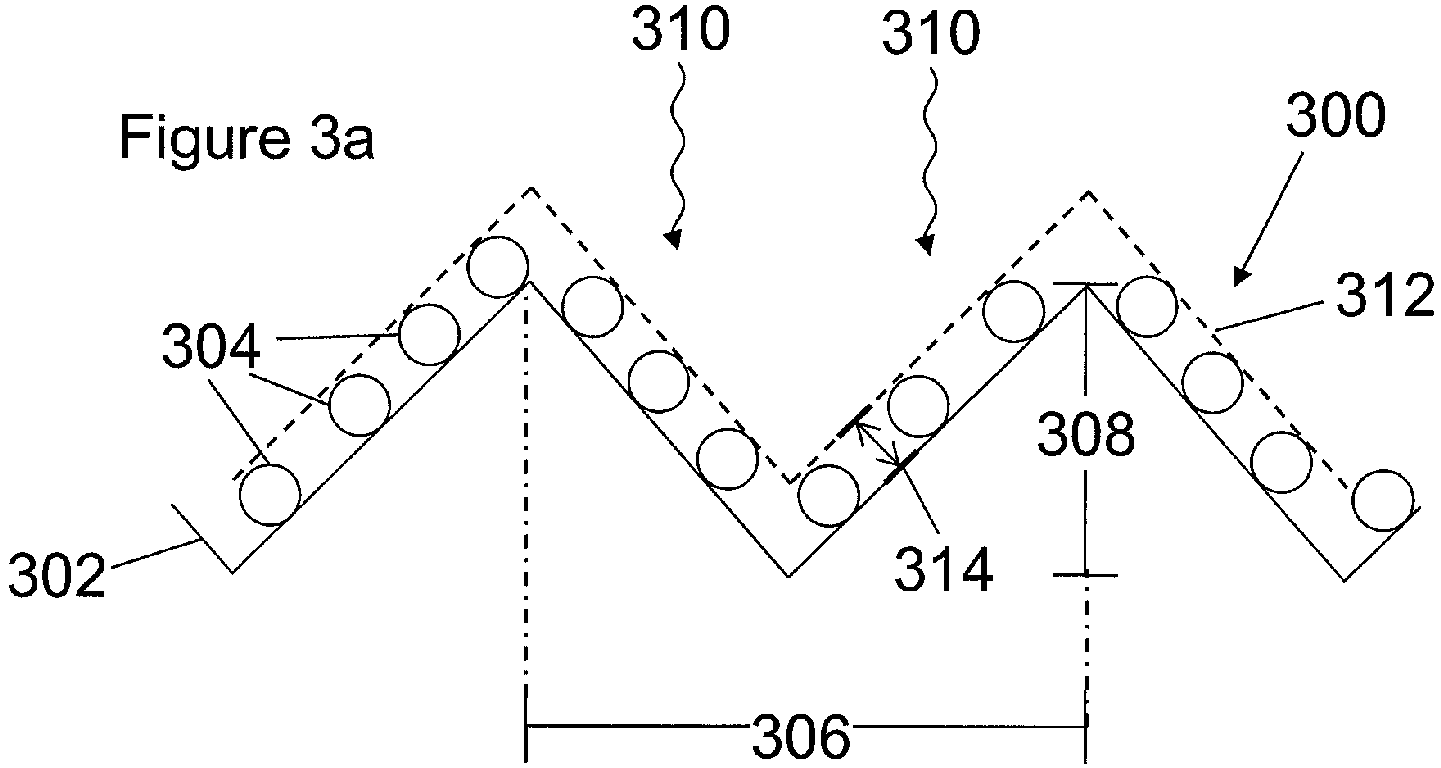
- the example apparatus 300 illustrated in Figure 3a comprises a two dimensional conductive channel 302 which may be provided with source and drain electrodes (not shown) configured to enable a flow of electrical current through the two dimensional conductive channel. Also shown is a quantum dot layer 304 overlying the two dimensional conductive channel 302. The quantum dot layer 304 is configured to generate charge on exposure to incident electromagnetic radiation 310. The generated charge produces an electric field which causes a change in electrical current passing through the underlying two dimensional conductive channel 302. The change in electrical current is indicative of one or more of the presence and magnitude of the incident electromagnetic radiation 310.
- the quantum dot layer 304 is configured to have an incident electromagnetic radiation surface 312 (that is, the surface 312 which is exposed to incident electromagnetic radiation 310, opposite to the surface in contact with the two dimensional conductive channel 302) which has a texturing comprising undulations in the surface.
- the texturing of the incident electromagnetic radiation surface 312 provides a surface roughness with an average peak amplitude 308 of the order of between 10nm and 300nm.
- the dimensions of the incident electromagnetic radiation surface 312 may be tuned to particular wavelengths of incident electromagnetic radiation. For example, a surface roughness with an average peak amplitude 308 of the order of between 10nm and 300nm may allow the apparatus 300 to detect incident electromagnetic radiation 310 having a wavelength of between about 200nm to about 1200nm.
- the surface roughness may have an average peak amplitude 308 of the order of between 10nm and 100nm. Such a range of average peak amplitudes 308 may allow the apparatus 300 to detect incident electromagnetic radiation 310 in the visible light range (i.e. electromagnetic radiation having a wavelength of between about 400nm to about 800nm.)
- the average peak separations 306 may also be tuned to a particular wavelength of incident electromagnetic radiation 310.
- the quantum dot layer 304 may be configured to have an incident electromagnetic radiation surface 312 which has a texturing comprising undulations in the surface to provide a surface roughness with an average peak separation 306 of the order of between 50nm and 2000nm.
- Such a range of average peak separation 306 may allow the apparatus 300 to detect electromagnetic radiation 310 having a wavelength of between about 200nm to about 1200nm.
- the surface roughness may have an average peak separation 306 of the order of between 50nm and 800nm. Such a range of average peak separation 306 may allow the apparatus to detect electromagnetic radiation 310 in the visible light range (i.e. electromagnetic radiation 310 having a wavelength of between about 400nm to about 800nm.)
- the surface roughness is provided by the quantum dot layer 304 conforming to an underlying surface texture provided to the two dimensional conductive channel 302.
- the quantum dot layer 304 may have a layer thickness 314 of the order of between 10nm and 500nm.
- the quantum dot layer 304 may have a layer thickness 314 of the order of approximately 100nm.
- Such a thickness 314 is advantageous as this provides a quantum dot layer 304 which is thick enough that the majority of quantum dots are available to actively participate in absorbing the incident electromagnetic radiation 310, while also being thin enough that the majority of quantum dots are in close enough proximity to the underlying two dimensional conductive channel to transfer charge created due to electromagnetic radiation absorption to the channel layer 302.
- the layer thickness 314 may be taken to be the thickness of the quantum dot layer 304 at a particular point normally through the quantum dot layer 304, normal to at least the incident electromagnetic radiation surface 312.
- the quantum dot layer may comprise a plurality of quantum dots formed from one or more of: PbS, CdSe, CdS, PbSe, ZnO, ZnS, CZTS, Cu 2 S, Bi 2 S 3 , Ag 2 S, HgTe, CdSe, CdHgTe, InAs, InSb, PbTe, CdTe, InP, ZnSe, CdSeTe, ZnSeS, ZnHgSe, ZnSeTe Ge and CIS. Practically, such compounds would ordinarily be in colloidal form for deposition.
- the two dimensional conductive channel in this and other examples may comprise one or more graphene layers, or may be one or more graphene layers.
- a single graphene layer is typically of the order ranging from 0.35 nm to 1 nm (i.e. approximately one carbon atom diameter) thick.
- the two dimensional conductive channel may be selected from the group of graphene-like materials such as phosphorene, germanen, etc., or the group of transition metal dichalcogenides (TMD): WX 2 , MoX 2 , ScX 2 , TiX 2 , HfX 2 , ZrX 2 , VX 2 , CrX 2 , MnX 2 , FeX 2 , CoX 2 , NiX 2 , NbX 2 , TcX 2 , ReX 2 , PdX 2 and PtX 2 wherein "X” may be S, Se or Te. ] All of the above materials may be provided as 2-D materials or few-layer materials, or their combination.
- TMD transition metal dichalcogenides
- a two-dimensional material is considered to have a maximum thickness of 1 nm (consistent with a single layer of atoms), in the context of the present disclosure it includes this understanding as well, in certain embodiments, it encompasses a few atomic layers, including 1-10 atomic layers/1-10nm thick layers. This, the understanding has been expanded to include low-dimensional materials as well, in certain embodiments.
- a photodetector may be fabricated in this way, namely comprising a layer of quantum dots at the surface configured to be exposed to light/electromagnetic radiation.
- Quantum dots comprising, for example, PbS and CdS may only partially absorb visible light with an external quantum efficiency (EQE) of around 10%-30%.
- Quantum dots made from these materials may also be able to absorb light over a broad spectrum, and therefore it may be challenging to use them in fabricating highly energy selective photodetectors.
- Such an apparatus with a textured surface may enable enhanced light scattering within the apparatus and enable enhanced light trapping, compared with a flat apparatus. Further, such an apparatus may increase the responsivity of the photodetector (e.g. through achieving a higher external quantum efficiency, EQE) and increase the wavelength selectivity (e.g. through achieving a selective EQE) of the apparatus.
- EQE external quantum efficiency
- the texturing of the surface 312 may comprise one or more texture shapes and/or one or more texture dimensions.
- a surface may be tuned for efficient absorption of a spectrum of incident visible light by texturing the surface with a range of surface undulation shapes/geometries and/or surface undulation dimensions to increase absorption of the visible light across the visible light wavelength range.
- the size and shape of texture may be adjusted to a target wavelength range for the photodetector to operate in.
- a mixture of patterned features may be used to form a pixel array, each pixel having a particular surface texture and thus a particular sensitivity to a particular wavelength or wavelength range of electromagnetic radiation.
- different wavelength sensitivity pixels may have different average peak amplitudes or peak separation for the texture of each pixel.
- such a detector could be used in different camera modes by filtering out the light received by a particular sensitive pixel type, for example infra-red radiation sensitive or visible light sensitive pixels.
- Such a detector would allow for the (simple) deposition of a single type of quantum dot over the differently surface-textured pixels and therefore there would be no requirement to use different materials for pixels of different wavelength sensitivity.
- the undulations in the incident electromagnetic radiation surface may have one or more particular shapes as shown in Figure 3b .
- the undulations providing the surface texture may comprise one or more of: periodic undulations 350, 352, 356, 358, 360, rounded pyramidal undulations 358, pyramidal undulations 350, 356, U-shaped undulations 360, hemispherical undulations 352, and/or irregular undulations 354.
- Inverted texture shapes may also be used, for example inverted pyramid structures or other suitable inverted structures.
- the two dimensional conductive channel e.g., a graphene sheet
- the two dimensional conductive channel overlays a textured substrate such that the two dimensional conductive channel substantially conforms to the underlying substrate texturing
- an undulation shape without sharp corners to help preserve the integrity of the overlying two dimensional conductive channel and reduce the possibility of cracks forming in the two dimensional conductive channel due to a sudden change of underlying substrate direction (i.e. folding over a sharp corner). Therefore, for example, surface textures such as those shown in Figure 3b with rounded corners 352, 354, 358, 360 may advantageously help the overlying two dimensional conductive channel to remain intact and avoid cracking/breaking.
- the flatness of the substrate is important for manufacturing devices having two dimensional conductive channels such as graphene channels
- the introduction of "large scale" features should not substantially affect the charge transport properties of the two dimensional conductive channel (e.g. graphene) layer.
- the texture of the polymer substrate may be smoothed by a variety of techniques, such as etching or nano-imprinting, if necessary for reducing nanoscale roughness (for example, to between 0.1 nm and 10nm) and helping maintain the integrity of the two dimensional conductive channel layer.
- Figures 4a and 4b illustrate example apparatuses which may be used as photodetectors.
- Figure 4a illustrates a photodetector 400 comprising a two dimensional conductive channel 408 with source and drain electrodes 404 configured to enable a flow of electrical current through the two dimensional conductive channel 408; and a quantum dot layer 406 overlying the two dimensional conductive channel 408.
- the quantum dot layer 406 is configured to have an incident electromagnetic radiation surface which has a texturing comprising undulations in the surface to provide a surface roughness with an average peak amplitude of the order of between 10nm and 300nm.
- a dielectric layer 410 (an insulator) underlying the two dimensional conductive channel 408, and a textured substrate 402 underlying the dielectric layer 410.
- the textured substrate 402 may comprise a polymer, for example. Polymer substrates may be advantageously used to provide a flexible apparatus 400.
- Figure 4b illustrates a field effect transistor (FET) 450 comprising a two dimensional conductive channel 408 with source and drain electrodes 404 configured to enable a flow of electrical current through the two dimensional conductive channel 408; and a quantum dot layer 406 overlying the two dimensional conductive channel 408.
- the quantum dot layer 406 is configured to have an incident electromagnetic radiation surface which has a texturing comprising undulations in the surface to provide a surface roughness with an average peak amplitude of the order of between 10nm and 300nm.
- an insulating dielectric layer 410 underlying the two dimensional conductive channel 408, a gate electrode layer 412 underlying the dielectric layer 410, such that the two dimensional conductive channel 408 is located between the dielectric layer 410 and the quantum dot layer 406.
- a textured substrate 402 underlying the gate electrode layer 412.
- the gate electrode layer 412 in this example is a bottom gate, or back gate 412 (although other gate configurations can be used).
- the substrate 402 may comprise a polymer, allowing the fabrication of a flexible FET 450.
- Figure 5 illustrates an example method of manufacture of a photodetector. This method may be termed a "polymer on graphene” method (if graphene is used as a two dimensional conductive channel and a polymer substrate is used).
- this method comprises texturing a substrate surface 502; depositing by direct growth the two dimensional conductive channel 506 over the textured substrate surface 502 so that it conforms to the underlying textured substrate surface 502 to provide a two dimensional textured conductive channel surface 506 having texturing comprising undulations in the surface; and depositing a layer of quantum dots 512 on the textured two dimensional conductive channel 506 such that the quantum dot layer 512 conforms to the textured surface to provide the surface roughness with an average peak amplitude of the order of between 10nm and 300nm.
- a textured donor substrate 502 is used.
- the donor substrate 502 may comprise, for example, silicon (Si) and/or silicon dioxide (SiO x ).
- Si silicon
- SiO x silicon dioxide
- the donor substrate 502 may be removed after fabrication of the apparatus by the SiO x acting as a release layer.
- the substrate 502 may be textured using etching or any other suitable method.
- Step 5a shows the provision of a sacrificial substrate layer 502 having a textured sacrificial substrate surface.
- Step 5b a metallic seed layer 504 is deposited onto the textured substrate 502 so that it conforms to the textured substrate 502.
- the metallic seed layer may comprise, for example, a metal such as copper, nickel, tungsten, rhenium, or other transition metals or their alloys.
- Step 5b shows the deposition of a metallic seed layer 504 onto the textured substrate 502 so that it conforms to the textured substrate 502.
- Step 5c the two dimensional conductive channel 506 is deposited onto the textured metallic seed layer 504 using chemical vapour deposition (CVD) so that it conforms to the underlying textured metallic seed layer 504 to provide the surface roughness to the incident electromagnetic radiation surface of the resulting apparatus.
- CVD chemical vapour deposition
- the two dimensional conductive channel 506 is deposited on the textured sacrificial substrate surface 502 (with an intervening metallic seed layer 504 in this example) so that it conforms to the textured sacrificial substrate surface 502, because the intervening metallic seed layer 504 also conforms to the textured sacrificial substrate surface 502.
- the CVD growth of the two dimensional conductive channel 506 on the textured metallic seed layer 504 may be achieved by careful selection of CVD growth parameters such as a growth temperature window, selected in order to achieve a continuous monolayer 506.
- CVD growth parameters such as a growth temperature window, selected in order to achieve a continuous monolayer 506.
- the two dimensional conductive channel 506 is textured by growing the layer 506 itself on a textured (sacrificial) substrate 502, 504.
- the graphene CVD deposition process may involve high temperatures up to 1000C.
- the polymer substrate deposited on graphene can be either hardened by UV light or thermally at relatively low temperatures typically below 150C. Any photolithography steps may involve the use of short temperature exposures up to 120C.
- a thin dielectric layer (for example, AlO x , SiN x ) can be deposited on top of the two dimensional conductive channel 506 in order to tune the graphene interface property for reducing the number of charge impurities or inhomogeneities and thus improving charge carrier transport in the graphene layer.
- a thin dielectric layer along with a gate layer can be used for providing a FET structure.
- a polymer layer 508 is cast/deposited against the two dimensional conductive channel layer 506 to form a shaped acceptor substrate 508.
- the electrodes 510 can be subsequently deposited or patterned from a metal catalyst layer as shown in Step 5f.
- the method shown in Figure 5 comprises releasing the sacrificial substrate layer 502 to expose (after etching away the metallic seed layer 504) the two dimensional conductive channel 506 having texturing comprising undulations in the surface to provide the surface roughness to the incident electromagnetic radiation surface.
- quantum dots 512 After the deposition of electrodes 510, quantum dots 512, and/or other functional layer(s) if required, can be coated or printed over the textured two dimensional conductive channel layer 506.
- the quantum dot layer 512 may form a conformal coating with uniform thickness, i.e. where the quantum dot layer 512 conforms to the texture of the underlying two dimensional conductive channel layer 506.
- a "double texture” may be introduced, for example by depositing a variable thickness quantum dot layer 512.
- Such a "double texture" apparatus may be used for wider light spectrum harvesting (that is, by having an incident electromagnetic radiation surface with two textures, one from the underlying textured two dimensional conductive channel 506 and a second texture form the quantum dot layer 512 itself, a broader range of electromagnetic radiation wavelengths may be absorbed by the device).
- a solution-processed quantum dot layer 512 may be deposited on top of a textured two dimensional conductive channel layer 506 such that the quantum dot layer 512 adds an extra roughness/texture with (for example) a smaller periodicity than the two dimensional conductive channel layer 506 texture.
- the smaller quantum dot layer 512 texture periodicity may be beneficial for absorption of shorter wavelength electromagnetic radiation, thereby providing a double texture broadening absorption spectrum.
- a bottom gate electrode and a gate dielectric may be included between the two dimensional conductive channel 506 and the polymer acceptor substrate 508 in order to complete a FET structure (as described above in relation to Figure 4b ).
- Figure 6 illustrates another example method of manufacture of a photodetector.
- This method may be termed a "direct deposition" method because the two dimensional conductive channel layer is deposited directly (e.g. transferred as a layer) onto the textured substrate (and any intervening layers such as dielectric layers, if used) without sacrificing a textured substrate and/or metallic seed layer as described in relation to Figure 5 .
- Step 6a shows a base substrate 602 onto which a liquid substrate polymer layer 608 is deposited.
- a master mould 614 is then used to imprint a texture into the liquid substrate polymer layer 608 resulting in a textured substrate polymer layer 608 after the polymer layer is solidified (for example, by curing, setting, or otherwise drying out/solidifying).
- the textured substrate polymer layer 608 is shown in Step 6b. Therefore these steps 6a and 6b show texturing of the underlying substrate surface 608, wherein the substrate 608 comprises a polymer; and the substrate surface 608 is textured by depositing the substrate as a liquid and imprinting the liquid substrate with a mould 614 to form the textured substrate surface 608.
- texturing the polymer layer 608 can be done by, for example, UV nanoimprinting or hot embossing. Such techniques to shape/texture the polymer substrate 608 may be performed before or after the process of applying the two dimensional conductive channel layer 606.
- Step 6c a thin dielectric layer 616 (for example, AlO x , SiN x ) is deposited over the polymer substrate layer 608 before transferring the two dimensional conductive channel 606.
- the dielectric layer 616 may help reduce any effects of two dimensional conductive channel 506-polymer 508 interfacing.
- a similar step may be performed between Step 5c and Step 5d of the previous example in Figure 5 .
- the dielectric layer 616 conforms to the underlying textured polymer substrate 602 to provide a textured surface.
- Step 6d the two dimensional conductive channel layer 606 (e.g., a graphene sheet) is transferred onto the textured dielectric layer 616.
- the two dimensional conductive channel layer 606 e.g., a graphene sheet
- transfer using a wet method PMMA based or other suitable solvent based may be performed to deposit the two dimensional conductive channel layer (the graphene layer) 606.
- the two dimensional conductive channel layer 606 may be applied such that it conforms to the texture of the underlying substrate 608, 616 without areas being "suspended" (i.e. not conforming) and without significant breakage of the layer 606.
- Step 6d shows deposition of the two dimensional conductive channel 606 over the textured substrate surface 608, 616 so that it conforms to the underlying textured substrate surface 608, 616 to provide a two dimensional textured conductive channel surface 606 having texturing comprising undulations in the surface.
- a dielectric layer may be deposited before depositing the two dimensional conductive channel 606, such that the two dimensional conductive channel 606 is located between the dielectric layer and the quantum dot layer 612 and the resulting apparatus may be used as a FET.
- Step 6e shows electrodes (e.g., source and drain electrodes) 610 being deposited.
- Step 6f shown the deposition of the quantum dot layer 612, conforming to the underlying textured two dimensional conductive channel layer 606.
- Step 6f shows deposition of a layer of quantum dots 612 on the textured two dimensional conductive channel 606 such that the quantum dot layer 612 conforms to the textured surface to provide the surface roughness with an average peak amplitude of the order of between 10nm and 300nm.
- Step 6g the initial substrate 602 used to support the initially liquid polymer 608 is removed.
- the polymer substrate deposited on graphene can be either hardened by UV light or thermally at relatively low temperatures typically below 150C.
- the photolithography steps may involve the use of short temperature exposures up to 120C.
- the dielectric deposition and patterning may also involve temperatures up to 120C.
- Figure 7 illustrates a further example method which differs from those described in relation to Figures 5 and 6 in that the quantum dot layer itself 712 comprises the surface roughness such that the incident electromagnetic radiation surface is independent of any underlying surface texture provided to the two dimensional conductive channel 706. That is, the quantum dot layer 712 is textured by having varying thickness, whereas the underlying substrate 706, 708, 716 is flat (i.e. planar, non-textured).
- double textured apparatus may be fabricated in which both the underlying substrate is textured, as well as the quantum dot layer itself being textured (i.e. having a variable thickness over its area).
- Step 7a shows the quantum dot layer 712 being provided by deposition of the quantum dot layer as a wet layer 712, in this example onto a two dimensional conductive channel 706 which is in turn on top of a dielectric layer 716 on a polymer substrate 708.
- the electrodes 710 are in place prior to the texturing of the quantum dot layer 712, but in other example may be deposited/provided after the quantum dot layer 712 has been textured.
- Step 7b shows imprinting of the wet quantum dot layer 712 with a textured mould 714 to provide the incident electromagnetic radiation surface with the surface roughness so that the quantum dot layer itself 712 comprises the surface roughness.
- the resulting apparatus is shown in Step 7c.
- Such a configuration may be less complex than exampled described above in which the two dimensional conductive channel itself is textured. Further, such a configuration may reduce the possibility of unwanted surface roughness at an interface between a dielectric layer (if present) and the two dimensional conductive channel 706.
- the quantum dot layer 712 may have a variable thickness as shown, providing the surface roughness with an average peak amplitude of the order of between 10nm and 300nm. In some examples the quantum dot layer 712 may have a variable thickness providing the surface roughness with an average peak separation of the order of between 50nm and 2000nm. In some examples the quantum dot layer 712 may have a layer thickness of the order of between 10nm and 500nm. The quantum dot layer 712 may have a layer thickness of the order of approximately 100nm. The responsivity of the photodetector may be dependent on the thickness of the quantum dot layer 712.
- Advantages of apparatus described herein in particular over devices having a planar surface without surface texturing, include increased light absorption.
- photodetectors as described herein may have increased responsivity (by trapping more light than an equivalent planar photodetector) and improved selectivity (by tuning the properties of the detector, such as choosing a particular undulation peak amplitude, undulation peak separation, quantum dot material).
- Local wavelength selectivity and amplification via texturing of the underlying two dimensional conductive channel may enable detectors to be made with different functions using the same broadband quantum dots.
- quantum dot / two dimensional conductor devices/apparatus as described herein using affordable methods of shaping polymers in different geometries.
- fabrication may be low cost, fast and involve low temperature processing if thermoset and UV curing polymers are used for substrate materials.
- Manufacture may be performed on large-area plastic/polymer foils/sheets at low cost.
- the devices may be made with mechanical flexibility and optical transparency (if using a transparent flexible polymer substrate and a flexible two dimensional conductive channel layer, such as graphene).
- the apparatus described herein may be used as visible light/infra-red light sensors or as X-ray detectors, for example.
- Figure 8 shows the main steps 802, 804, 806 of a method of making the present apparatus.
- the method generally providing a two dimensional conductive channel 802; providing source and drain electrodes configured to enable a flow of electrical current through the two dimensional conductive channel 804; and providing a quantum dot layer overlying the two dimensional conductive channel 806, the quantum dot layer configured to generate charge on exposure to incident electromagnetic radiation, the generated charge producing an electric field which causes a change in electrical current passing through the underlying two dimensional conductive channel, the change in electrical current indicative of one or more of the presence and magnitude of the incident electromagnetic radiation; wherein the quantum dot layer is configured to have an incident electromagnetic radiation surface which has a texturing comprising undulations in the surface to provide a surface roughness with an average peak amplitude of the order of between 10nm and 300nm.
- Figure 9 illustrates schematically a computer/processor readable medium 900 providing a computer program according to one embodiment.
- the computer program comprises computer code configured to perform, control or enable one or more of the method steps of Figure 8 .
- the computer/processor readable medium 900 is a disc such as a digital versatile disc (DVD) or a compact disc (CD).
- DVD digital versatile disc
- CD compact disc
- the computer/processor readable medium 900 may be any medium that has been programmed in such a way as to carry out an inventive function.
- the computer/processor readable medium 900 may be a removable memory device such as a memory stick or memory card (SD, mini SD, micro SD or nano SD).
- any mentioned apparatus/device and/or other features of particular mentioned apparatus/device may be provided by apparatus arranged such that they become configured to carry out the desired operations only when enabled, e.g. switched on, or the like. In such cases, they may not necessarily have the appropriate software loaded into the active memory in the non-enabled (e.g. switched off state) and only load the appropriate software in the enabled (e.g. on state).
- the apparatus may comprise hardware circuitry and/or firmware.
- the apparatus may comprise software loaded onto memory.
- Such software/computer programs may be recorded on the same memory/processor/functional units and/or on one or more memories/processors/functional units.
- a particular mentioned apparatus/device may be pre-programmed with the appropriate software to carry out desired operations, and wherein the appropriate software can be enabled for use by a user downloading a "key", for example, to unlock/enable the software and its associated functionality.
- Advantages associated with such embodiments can include a reduced requirement to download data when further functionality is required for a device, and this can be useful in examples where a device is perceived to have sufficient capacity to store such pre-programmed software for functionality that may not be enabled by a user.
- any mentioned apparatus/circuitry/elements/processor may have other functions in addition to the mentioned functions, and that these functions may be performed by the same apparatus/circuitry/elements/processor.
- One or more disclosed aspects may encompass the electronic distribution of associated computer programs and computer programs (which may be source/transport encoded) recorded on an appropriate carrier (e.g. memory, signal).
- any "computer” described herein can comprise a collection of one or more individual processors/processing elements that may or may not be located on the same circuit board, or the same region/position of a circuit board or even the same device. In some embodiments one or more of any mentioned processors may be distributed over a plurality of devices. The same or different processor/processing elements may perform one or more functions described herein.
- signal may refer to one or more signals transmitted as a series of transmitted and/or received signals.
- the series of signals may comprise one, two, three, four or even more individual signal components or distinct signals to make up said signalling. Some or all of these individual signals may be transmitted/received simultaneously, in sequence, and/or such that they temporally overlap one another.
- processors and memory may comprise a computer processor, Application Specific Integrated Circuit (ASIC), field-programmable gate array (FPGA), and/or other hardware components that have been programmed in such a way to carry out the inventive function.
- ASIC Application Specific Integrated Circuit
- FPGA field-programmable gate array
Landscapes
- Light Receiving Elements (AREA)
- Engineering & Computer Science (AREA)
- Manufacturing & Machinery (AREA)
- Solid State Image Pick-Up Elements (AREA)
Abstract
Description
- The present disclosure relates to the field of two-dimensional materials and electronic devices such as photodetectors and field effect transistors (FETs) comprising two-dimensional materials.
- Certain aspects/embodiments may relate to sensing (e.g. optical sensing) and imaging for healthcare, automotive or wearable applications. Other disclosed example aspects/embodiments relate to portable electronic devices, in particular, so-called hand-portable electronic devices which may be hand-held in use (although they may be placed in a cradle in use). Such hand-portable electronic devices include so-called Personal Digital Assistants (PDAs) and tablet PCs.
- The portable electronic devices/apparatus according to one or more disclosed example aspects/embodiments may provide one or more audio/text/video communication functions (e.g. tele-communication, video-communication, and/or text transmission, Short Message Service (SMS)/ Multimedia Message Service (MMS)/emailing functions, interactive/non-interactive viewing functions (e.g. web-browsing, navigation, TV/program viewing functions), music recording/playing functions (e.g. MP3 or other format and/or (FM/AM) radio broadcast recording/playing), downloading/sending of data functions, image capture function (e.g. using a (e.g. in-built) digital camera), and gaming functions.
- Electronic apparatus may be fabricated using two-dimensional materials, such as graphene.
- The listing or discussion of a prior-published document or any background in this specification should not necessarily be taken as an acknowledgement that the document or background is part of the state of the art or is common general knowledge.
- According to a first aspect, there is provided an apparatus comprising
a two dimensional conductive channel with source and drain electrodes configured to enable a flow of electrical current through the two dimensional conductive channel; and
a quantum dot layer overlying the two dimensional conductive channel, the quantum dot layer configured to generate charge on exposure to incident electromagnetic radiation, the generated charge producing an electric field which causes a change in electrical current passing through the underlying two dimensional conductive channel, the change in electrical current indicative of one or more of the presence and magnitude of the incident electromagnetic radiation;
wherein the quantum dot layer is configured to have an incident electromagnetic radiation surface which has a texturing comprising undulations in the surface to provide a surface roughness with an average peak amplitude of the order of between 10nm and 300nm. - Such a range of average peak amplitudes may allow the apparatus to detect electromagnetic radiation having a wavelength of between about 200nm to about 1200nm.
- The average peak amplitude may be of the order of between various combinations of 10nm, 15nm, 20nm, 25nm, 30nm, 35nm, 40nm, 45nm, 50nm, 55nm, 60nm, 65nm, 70nm, 75nm, 80nm, 85nm, 90mn, 95nm, 100nm, 105nm, 110nm, 115nm, 120nm, 125nm, 130nm, 135nm, 140nm, 145nm, 150nm, and 155nm, 160nm, 165nm, 170nm, 175nm, 180nm, 185nm, 190nm, 195nm, 200nm, 205nm, 210nm, 215nm, 220nm, 225nm, 230nm, 235nm, 240nm, 245nm, 250nm, 255nm, 260nm, 265nm, 270nm, 275nm, 280nm, 285nm, 290nm, 295nm, and 300nm. That, is, the average peak amplitude may be of the order of between 10nm to 150nm, and 155nm to 300nm (for example, between 45nm and 270nm, or between 80nm and 250nm).
- The surface roughness may have an average peak amplitude of the order of between 10nm and 100nm. Such a range of average peak amplitudes may allow the apparatus to detect electromagnetic radiation in the visible light range (i.e. electromagnetic radiation having a wavelength of between about 400nm to about 800nm.)
- The quantum dot layer may be configured to have an incident electromagnetic radiation surface which has a texturing comprising undulations in the surface to provide a surface roughness with an average peak separation of the order of between 50nm and 2000nm.
- Such a range of average peak separation may allow the apparatus to detect electromagnetic radiation having a wavelength of between about 200nm to about 1200nm.
- The surface roughness may have an average peak separation of the order of between 50nm and 800nm. Such a range of average peak separation may allow the apparatus to detect electromagnetic radiation in the visible light range (i.e. electromagnetic radiation having a wavelength of between about 400nm to about 800nm.)
- Accordingly, the textured incident electromagnetic radiation surface may be configured to reduce reflection of incident electromagnetic radiation compared with a non-textured incident electromagnetic radiation surface.
- The surface roughness may be provided by one or more of:
- the quantum dot layer conforming to an underlying surface texture provided to the two dimensional conductive channel; and
- the quantum dot layer itself comprising the surface roughness such that the incident electromagnetic radiation surface is at least independent of any underlying surface texture provided to the two dimensional conductive channel.
- The surface roughness may be provided by one or more of:
- the quantum dot layer having a variable thickness providing the surface roughness with an average peak amplitude of the order of between 10nm and 300nm; and
- the underlying surface texture provided to the two dimensional conductive channel providing the surface roughness with an average peak amplitude of the order of between 10nm and 300nm.
- The surface roughness may be provided by one or more of:
- the quantum dot layer having a variable thickness providing the surface roughness with an average peak separation of the order of between 50nm and 2000nm; and
- the underlying surface texture provided to the two dimensional conductive channel providing the surface roughness with an average peak separation of the order of between 50nm and 2000nm.
- The quantum dot layer may have a layer thickness of the order of between 10nm and 500nm. The quantum dot layer may have a layer thickness of the order of approximately 100nm. The layer thickness may be taken to be the thickness of the quantum dot layer at a particular point normally through the quantum dot layer, normal to at least the incident electromagnetic radiation surface.
- The two dimensional conductive channel may comprise graphene.
- The quantum dot layer may comprise a plurality of quantum dots formed from one or more of: PbS, CdSe, CdS, PbSe, ZnO, ZnS, CZTS, Cu2S, Bi2S3, Ag2S, HgTe, CdSe, CdHgTe, InAs, InSb, PbTe, CdTe, InP, ZnSe, CdSeTe, ZnSeS, ZnHgSe, ZnSeTeGe and CIS. The quantum dot layer/film may be deposited from colloidal quantum dots (or may comprise colloidal quantum dots). It will be appreciated that colloidal quantum dots are considered to be quantum dots dispersed/suspended in solution so that they do not settle to the bottom of a container.
- The undulations in the incident electromagnetic radiation surface may comprise one or more of: periodic undulations, rounded pyramidal undulations, pyramidal undulations, U-shaped undulations, hemispherical undulations, and irregular undulations.
- The apparatus may further comprise:
- a dielectric layer underlying the two dimensional conductive channel; and
- a gate layer underlying the dielectric layer, such that
- the two dimensional conductive channel is located between the dielectric layer and the quantum dot layer.
- The apparatus may be one or more of: an electronic device, a portable electronic device, a portable telecommunications device, a mobile phone, a personal digital assistant, a tablet computer, a desktop computer, a laptop computer, a server, a smartphone, a smartwatch, smart eyewear, a camera, a sensor, an image sensor, a photodetector, a phototransistor, a flat panel array comprising a plurality of detection pixels, and a module for one or more of the same.
- According to a further aspect, there is provided a method comprising:
- providing a two dimensional conductive channel;
- providing source and drain electrodes configured to enable a flow of electrical current through the two dimensional conductive channel; and
- providing a quantum dot layer overlying the two dimensional conductive channel, the quantum dot layer configured to generate charge on exposure to incident electromagnetic radiation, the generated charge producing an electric field which causes a change in electrical current passing through the underlying two dimensional conductive channel, the change in electrical current indicative of one or more of the presence and magnitude of the incident electromagnetic radiation;
- wherein the quantum dot layer is configured to have an incident electromagnetic radiation surface which has a texturing comprising undulations in the surface to provide a surface roughness with an average peak amplitude of the order of between 10nm and 300nm.
- Providing the quantum dot layer may comprise one or more of:
- depositing a layer of quantum dots so that it conforms with an underlying surface texture provided to the two dimensional conductive channel; and
- depositing a layer of quantum dots such that the layer of quantum dots itself has the surface roughness such that the incident electromagnetic radiation surface which is at least independent of any underlying surface texture provided to the two dimensional conductive channel.
- Providing the quantum dot layer may comprise depositing the quantum dot layer as a wet layer, and imprinting the wet quantum dot layer with a textured mould to provide the incident electromagnetic radiation surface of the quantum dot layer with the surface roughness. The mould face which engages with the wet layer may have a textured surface with an average peak amplitude of the order of between 10nm and 300nm, or appropriate sub-ranges thereof, as discussed earlier in relation to the average peak amplitude of the textured incident electromagnetic radiation surface of the quantum dot layer.
- The method may comprise:
- texturing a substrate surface;
- depositing the two dimensional conductive channel over the textured substrate surface so that it conforms to the underlying textured substrate surface to provide a two dimensional textured conductive channel surface having texturing comprising undulations in the surface; and
- depositing a layer of quantum dots on the textured two dimensional conductive channel such that the quantum dot layer conforms to the textured surface to provide the surface roughness with an average peak amplitude of the order of between 10nm and 300nm.
- The substrate surface texturing may have an average peak amplitude of the order of between 10nm and 300nm, or appropriate sub-ranges thereof, as discussed earlier in relation to the average peak amplitude of the textured incident electromagnetic radiation surface of the quantum dot layer.
- The term "conforms" may be taken to mean that, for example, the two dimensional conductive channel substantially follows the contours of the underlying textured surface of the substrate, and/or, for example, the quantum dot layer substantially follows the contours of the underlying textured two dimensional conductive channel.
- The substrate may comprise a polymer; and the substrate surface may be textured by depositing the substrate as a liquid and imprinting the liquid substrate with a mould to form the textured substrate surface.
- The substrate may comprise silicon and/or silicon dioxide; and the substrate surface may be textured by wet etching, dry etching, electron-beam lithography, focused ion beam (FIB) lithography, or other suitable technique.
- The method may comprise:
- depositing a metallic seed layer onto the textured substrate so that it conforms to the textured substrate; and
- depositing the two dimensional conductive channel onto the textured metallic seed layer using chemical vapour deposition so that it conforms to the underlying textured metallic seed layer to provide the surface roughness to the incident electromagnetic radiation surface.
- The method may comprise:
- providing a sacrificial substrate layer having a textured sacrificial substrate surface;
- depositing the two dimensional conductive channel on the textured sacrificial substrate surface so that it conforms to the textured sacrificial substrate surface;
- depositing a polymer layer onto the two dimensional conductive channel; and
- releasing the sacrificial substrate layer to expose the two dimensional conductive channel having texturing comprising undulations in the surface to provide the surface roughness to the incident electromagnetic radiation surface.
- The method may comprise depositing electrodes on the two dimensional conductive channel to allow for the flow of charge through the two dimensional conductive channel between the deposited electrodes.
- The method may comprise:
- depositing a gate layer prior to depositing a dielectric layer; and
- depositing the dielectric layer prior to depositing the two dimensional conductive channel; such that
- the two dimensional conductive channel is located between the dielectric layer and the quantum dot layer.
- The steps of any method disclosed herein do not have to be performed in the exact order disclosed, unless explicitly stated or understood by the skilled person.
- According to a further aspect, there is provided a computer readable medium comprising computer program code stored thereon, the computer readable medium and computer program code being configured to, when run on at least one processor, perform any of the methods disclosed herein.
- Corresponding computer programs (which may or may not be recorded on a carrier) for implementing one or more of the methods disclosed herein are also within the present disclosure and encompassed by one or more of the described example embodiments.
- Throughout the present specification, descriptors relating to relative orientation and position, such as "top", "bottom", "left", "right", "above" and "below", as well as any adjective and adverb derivatives thereof, are used in the sense of the orientation of the apparatus as presented in the drawings. However, such descriptors are not intended to be in any way limiting to an intended use of the described examples.
- References to "light" throughout this specification may be understood to encompass the visible light wavelength range of the electromagnetic spectrum as well as other wavelength ranges of the electromagnetic spectrum; similarly references to the "electromagnetic spectrum" of course include the visible light wavelength range as well as other wavelength ranges (e.g., infra-red, ultra-violet, and others).
- References to "layer" throughout this specification are intended to encompass a single layer in the sense of a monolayer (e.g., a monolayer of graphene), a layer in the sense of a multilayer comprising multiple layers of substantially a single material (e.g., a multilayer of copper several atoms thick, a polymer layer of the order of 100nm, 1µm or 1 mm) and also a multilayer in the sense of a functional layer component comprising more than one layer material (e.g., a substrate layer comprising a plurality of layers of different materials), and also a combination of these.
- The present disclosure includes one or more corresponding aspects, example embodiments or features in isolation or in various combinations whether or not specifically stated (including claimed) in that combination or in isolation. Corresponding means and corresponding functional units for performing one or more of the discussed functions are also within the present disclosure.
- The above summary is intended to be merely exemplary and non-limiting.
- A description is now given, by way of example only, with reference to the accompanying drawings, in which:-
-
Figure 1 illustrates light interacting with a surface; -
Figure 2 illustrates schematically an apparatus according to examples described herein; -
Figure 3a illustrates an apparatus and dimensions thereof according to examples described herein; -
Figure 3b illustrates possible surface roughness profiles of an apparatus according to examples described herein; -
Figure 4a illustrates an example photodetector apparatus according to examples described herein; -
Figure 4b illustrates an example field effect transistor apparatus according to examples described herein; -
Figure 5 illustrates a method of making an apparatus according to examples described herein; -
Figure 6 illustrates another method of making an apparatus to examples described herein; -
Figure 7 illustrates another method of making an apparatus to examples described herein; -
Figure 8 illustrates schematically a method of making an apparatus according to examples disclosed herein; and -
Figure 9 shows a computer-readable medium comprising a computer program configured to perform, control or enable the method ofFigure 8 . - One or more disclosed embodiments of the present apparatus relate to photodetectors. A photodetector is a device/apparatus which can operate to detect/sense the presence of visible light or other electromagnetic energy/radiation.
- A common problem of photosensitive devices is that light approaching the surface may be absorbed weakly which makes absorption enhancement desirable to obtain a feasible device. Photosensitive devices such as photodetectors require a promotion of the response of light from a limited wavelength range (e.g. visible light). It may therefore be desirable to enhance light absorption in photosensitive devices such as photodetectors.
- Surface texturing may provide a way of reducing the reflection of light incident on the surface of a photosensitive device compared with reflection from a flat non-textured surface, and increasing the probability of light scattering inside the structure of the device. Any "roughening" of the surface may reduce light reflection by increasing the chances of reflected light bouncing back onto the surface, rather than out to the surroundings. This principle is illustrated in
Figure 1 . -
Incident light 102 may be trapped 104 inside a material 150 (rather than reflecting off 106, 108 the material's surface) by changing the angle θ1 at which light 102 is incident on and travels in thematerial 150. The angle at which light is refracted into amaterial 150 is n1 sinθ1 =n2 sinθ 2 according to Snell's Law, where θ1 and θ 2 are the angles for the light incident on the interface relative to the normal plane, and n1 and n2 are the refractive indices of theinterface media - By rearranging Snell's law, the angle at which light enters the
material 150 on which it is incident (the angle of refracted light) can be calculated by θ2 =sin-1(n2 sinθ1 /n1 ). The amount of light reflected 106, 108 at an interface can be calculated from the Fresnel reflection formula. For light polarised parallel to the surface, for light polarised perpendicular to the surface, and for unpolarised light, the amount of reflected light R∥, R⊥ and RT respectively, is:


- Increasing the amount of light trapped, for example, in a photodetector, may be advantageous to increase the efficiency of the photodetector.
- Fabricating a photodetector as an apparatus comprising quantum dots overlaying a two-dimensional conductor so that the surface of the apparatus open for light/electromagnetic radiation exposure has a texture to increase the amount of light/electromagnetic radiation absorbed compared with a flat (non-textured) apparatus may be performed according to examples described herein.
- Examples described herein relate to an apparatus comprising: a two dimensional conductive channel with source and drain electrodes configured to enable a flow of electrical current through the two dimensional conductive channel; and a quantum dot layer overlying the two dimensional conductive channel, the quantum dot layer configured to generate charge on exposure to incident electromagnetic radiation, the generated charge producing an electric field which causes a change in electrical current passing through the underlying two dimensional conductive channel, the change in electrical current indicative of one or more of the presence and magnitude of the incident electromagnetic radiation; wherein the quantum dot layer is configured to have an incident electromagnetic radiation surface which has a texturing comprising undulations in the surface to provide a surface roughness with an average peak amplitude of the order of between 10nm and 300nm.
- The average peak amplitude may be taken to mean the arithmetic mean value of peak amplitudes, for example for a sample area of the textured surface. Similarly the average peak separation may be taken to mean the arithmetic mean of peak separations for a sample area of the textured surface (for example, as measured in one or more directions over the surface). It may be understood that an "outlier" feature, such as a scratch in the surface, is not taken to contribute to the average peak amplitude and/or average peak separation.
-
Figure 2 shows anexample apparatus 201 comprising acomponent apparatus 250 as described herein. Theapparatus 201 may be one or more of: an electronic device, a portable electronic device, a portable telecommunications device, a mobile phone, a personal digital assistant, a tablet computer, a desktop computer, a laptop computer, a server, a smartphone, a smartwatch, smart eyewear, a camera, a sensor, an image sensor, a photodetector, a phototransistor, a flat panel array comprising a plurality of detection pixels, and a module for one or more of the same. In certain examples, the apparatus may comprise amemory 203,processor 202 andcomponent apparatus 250. - In this example, the
apparatus 201 comprises aprocessor 202, amemory 203, atransceiver 204, apower supply 205, acomponent apparatus 250, and may comprise anelectronic display 206 and aloudspeaker 207, which are electrically connected to one another by adata bus 208. - The
processor 202 is configured for general operation of theapparatus 201 by providing signalling to, and receiving signalling from, the other components to manage their operation. Thememory 203 is configured to store computer program code configured to perform, control or enable operation of theapparatus 201. Thememory 203 may also be configured to store settings for the other components. Theprocessor 202 may access thememory 203 to retrieve the component settings in order to manage the operation of the other components. Theprocessor 202 may be a microprocessor, including an Application Specific Integrated Circuit (ASIC). Thememory 203 may comprise a temporary storage medium such as a volatile random access memory, and/or may comprise a permanent storage medium such as a hard disk drive, a flash memory, or a non-volatile random access memory. Thepower supply 205 is configured to provide the other components with electrical power to enable their functionality. - Certain examples may comprise a
transceiver 204, and others not. In the former examples, thetransceiver 204 may be configured to transmit data to, and/or receive data from, other apparatus/devices. Certain examples may comprise anelectronic display 206. In such examples, theelectronic display 206 may be include LED, e-ink, or LCD display, and be configured to display visual content. Similarly, certain examples may comprise aloudspeaker 207; and in such examples, theloudspeaker 207 may be configured to output audio content which is stored on or received by theapparatus 201. In other examples, thedisplay 206,loudspeaker 207 and any user interface components may be remote to, but in communication with, theapparatus 201 rather than forming part of theapparatus 201. Further, in other examples, thepower supply 205 may be housed separately from theapparatus 201, and may be mains power. - The
component apparatus 250 may be considered to be an electronic component and may be configured to operate as a photodiode, sensor, or field effect transistor (FET), for example. Thecomponent apparatus 250 comprises, as described in more detail below, a two dimensional conductive channel with source and drain electrodes configured to enable a flow of electrical current through the two dimensional conductive channel; and a quantum dot layer overlying the two dimensional conductive channel, the quantum dot layer configured to generate charge on exposure to incident electromagnetic radiation, the generated charge producing an electric field which causes a change in electrical current passing through the underlying two dimensional conductive channel, the change in electrical current indicative of one or more of the presence and magnitude of the incident electromagnetic radiation; wherein the quantum dot layer is configured to have an incident electromagnetic radiation surface which has a texturing comprising undulations in the surface to provide an surface roughness with an average peak amplitude of the order of between 10nm and 300nm. - In general, the textured incident electromagnetic radiation surface of the
apparatus 250 may be configured to reduce reflection of incident electromagnetic radiation compared with a non-textured incident electromagnetic radiation surface. This may be achieved by increasing the amount of light which is absorbed by the apparatus, for example, by providing an incident electromagnetic radiation surface having a textured geometry which increases the number of times that reflected electromagnetic radiation hits the incident electromagnetic radiation surface, thereby increasing the chance that the light is absorbed. For example, with reference toFigure 1 , the reflectedelectromagnetic radiation 106 which was not absorbed the first time the incidentelectromagnetic radiation 102 hit the surface is (partially) absorbed the second time it hits the surface, with a reflectedproportion 108. Such absorption of reflected electromagnetic radiation would not occur if theincident radiation 102 hit a flat surface. - The
example apparatus 300 illustrated inFigure 3a comprises a two dimensionalconductive channel 302 which may be provided with source and drain electrodes (not shown) configured to enable a flow of electrical current through the two dimensional conductive channel. Also shown is aquantum dot layer 304 overlying the two dimensionalconductive channel 302. Thequantum dot layer 304 is configured to generate charge on exposure to incidentelectromagnetic radiation 310. The generated charge produces an electric field which causes a change in electrical current passing through the underlying two dimensionalconductive channel 302. The change in electrical current is indicative of one or more of the presence and magnitude of the incidentelectromagnetic radiation 310. - The
quantum dot layer 304 is configured to have an incident electromagnetic radiation surface 312 (that is, thesurface 312 which is exposed to incidentelectromagnetic radiation 310, opposite to the surface in contact with the two dimensional conductive channel 302) which has a texturing comprising undulations in the surface. The texturing of the incidentelectromagnetic radiation surface 312 provides a surface roughness with anaverage peak amplitude 308 of the order of between 10nm and 300nm. - The dimensions of the incident
electromagnetic radiation surface 312 may be tuned to particular wavelengths of incident electromagnetic radiation. For example, a surface roughness with anaverage peak amplitude 308 of the order of between 10nm and 300nm may allow theapparatus 300 to detect incidentelectromagnetic radiation 310 having a wavelength of between about 200nm to about 1200nm. - In some examples, the surface roughness may have an
average peak amplitude 308 of the order of between 10nm and 100nm. Such a range ofaverage peak amplitudes 308 may allow theapparatus 300 to detect incidentelectromagnetic radiation 310 in the visible light range (i.e. electromagnetic radiation having a wavelength of between about 400nm to about 800nm.) - As well as the
average peak amplitudes 308 being tuneable to a particular wavelength of incident electromagnetic radiation, theaverage peak separations 306 may also be tuned to a particular wavelength of incidentelectromagnetic radiation 310. For example, thequantum dot layer 304 may be configured to have an incidentelectromagnetic radiation surface 312 which has a texturing comprising undulations in the surface to provide a surface roughness with anaverage peak separation 306 of the order of between 50nm and 2000nm. Such a range ofaverage peak separation 306 may allow theapparatus 300 to detectelectromagnetic radiation 310 having a wavelength of between about 200nm to about 1200nm. - In some examples, the surface roughness may have an
average peak separation 306 of the order of between 50nm and 800nm. Such a range ofaverage peak separation 306 may allow the apparatus to detectelectromagnetic radiation 310 in the visible light range (i.e.electromagnetic radiation 310 having a wavelength of between about 400nm to about 800nm.) - In this example, the surface roughness is provided by the
quantum dot layer 304 conforming to an underlying surface texture provided to the two dimensionalconductive channel 302. - The
quantum dot layer 304 may have alayer thickness 314 of the order of between 10nm and 500nm. Thequantum dot layer 304 may have alayer thickness 314 of the order of approximately 100nm. Such athickness 314 is advantageous as this provides aquantum dot layer 304 which is thick enough that the majority of quantum dots are available to actively participate in absorbing the incidentelectromagnetic radiation 310, while also being thin enough that the majority of quantum dots are in close enough proximity to the underlying two dimensional conductive channel to transfer charge created due to electromagnetic radiation absorption to thechannel layer 302. Thelayer thickness 314 may be taken to be the thickness of thequantum dot layer 304 at a particular point normally through thequantum dot layer 304, normal to at least the incidentelectromagnetic radiation surface 312. - The quantum dot layer may comprise a plurality of quantum dots formed from one or more of: PbS, CdSe, CdS, PbSe, ZnO, ZnS, CZTS, Cu2S, Bi2S3, Ag2S, HgTe, CdSe, CdHgTe, InAs, InSb, PbTe, CdTe, InP, ZnSe, CdSeTe, ZnSeS, ZnHgSe, ZnSeTe Ge and CIS. Practically, such compounds would ordinarily be in colloidal form for deposition.
- The two dimensional conductive channel in this and other examples may comprise one or more graphene layers, or may be one or more graphene layers. A single graphene layer is typically of the order ranging from 0.35 nm to 1 nm (i.e. approximately one carbon atom diameter) thick. In other examples the two dimensional conductive channel may be selected from the group of graphene-like materials such as phosphorene, germanen, etc., or the group of transition metal dichalcogenides (TMD): WX2, MoX2, ScX2, TiX2, HfX2, ZrX2, VX2, CrX2, MnX2, FeX2, CoX2, NiX2, NbX2, TcX2, ReX2, PdX2 and PtX2 wherein "X" may be S, Se or Te. ] All of the above materials may be provided as 2-D materials or few-layer materials, or their combination. Although ordinarily a two-dimensional material is considered to have a maximum thickness of 1 nm (consistent with a single layer of atoms), in the context of the present disclosure it includes this understanding as well, in certain embodiments, it encompasses a few atomic layers, including 1-10 atomic layers/1-10nm thick layers. This, the understanding has been expanded to include low-dimensional materials as well, in certain embodiments.
- A photodetector may be fabricated in this way, namely comprising a layer of quantum dots at the surface configured to be exposed to light/electromagnetic radiation. Quantum dots comprising, for example, PbS and CdS may only partially absorb visible light with an external quantum efficiency (EQE) of around 10%-30%. Quantum dots made from these materials may also be able to absorb light over a broad spectrum, and therefore it may be challenging to use them in fabricating highly energy selective photodetectors. By texturing the incident electromagnetic radiation surface using particular surface undulation dimensions, the sensitivity to a particular wavelength range of incident electromagnetic radiation may be achieved and may therefore increase the responsivity of the apparatus.
- Such an apparatus with a textured surface may enable enhanced light scattering within the apparatus and enable enhanced light trapping, compared with a flat apparatus. Further, such an apparatus may increase the responsivity of the photodetector (e.g. through achieving a higher external quantum efficiency, EQE) and increase the wavelength selectivity (e.g. through achieving a selective EQE) of the apparatus.
- The texturing of the
surface 312 may comprise one or more texture shapes and/or one or more texture dimensions. For example, a surface may be tuned for efficient absorption of a spectrum of incident visible light by texturing the surface with a range of surface undulation shapes/geometries and/or surface undulation dimensions to increase absorption of the visible light across the visible light wavelength range. In other words, the size and shape of texture may be adjusted to a target wavelength range for the photodetector to operate in. - A mixture of patterned features may be used to form a pixel array, each pixel having a particular surface texture and thus a particular sensitivity to a particular wavelength or wavelength range of electromagnetic radiation. For example, different wavelength sensitivity pixels may have different average peak amplitudes or peak separation for the texture of each pixel. In the example of a series of different-sensitivity pixels spaced across the surface of a detector, such a detector could be used in different camera modes by filtering out the light received by a particular sensitive pixel type, for example infra-red radiation sensitive or visible light sensitive pixels. Such a detector would allow for the (simple) deposition of a single type of quantum dot over the differently surface-textured pixels and therefore there would be no requirement to use different materials for pixels of different wavelength sensitivity.
- The undulations in the incident electromagnetic radiation surface may have one or more particular shapes as shown in
Figure 3b . For example, the undulations providing the surface texture may comprise one or more of:periodic undulations pyramidal undulations 358,pyramidal undulations U-shaped undulations 360,hemispherical undulations 352, and/orirregular undulations 354. Inverted texture shapes may also be used, for example inverted pyramid structures or other suitable inverted structures. - In an apparatus in which the two dimensional conductive channel (e.g., a graphene sheet) overlays a textured substrate such that the two dimensional conductive channel substantially conforms to the underlying substrate texturing, it may be advantageous to use an undulation shape without sharp corners to help preserve the integrity of the overlying two dimensional conductive channel and reduce the possibility of cracks forming in the two dimensional conductive channel due to a sudden change of underlying substrate direction (i.e. folding over a sharp corner). Therefore, for example, surface textures such as those shown in
Figure 3b withrounded corners - While the flatness of the substrate (i.e. with a low surface roughness) is important for manufacturing devices having two dimensional conductive channels such as graphene channels, the introduction of "large scale" features (for example, between 50nm and 1000nm in size), in particular with a smooth profile (rather than angular corners) should not substantially affect the charge transport properties of the two dimensional conductive channel (e.g. graphene) layer. Furthermore, the texture of the polymer substrate may be smoothed by a variety of techniques, such as etching or nano-imprinting, if necessary for reducing nanoscale roughness (for example, to between 0.1 nm and 10nm) and helping maintain the integrity of the two dimensional conductive channel layer.
-
Figures 4a and 4b illustrate example apparatuses which may be used as photodetectors.Figure 4a illustrates aphotodetector 400 comprising a two dimensionalconductive channel 408 with source and drainelectrodes 404 configured to enable a flow of electrical current through the two dimensionalconductive channel 408; and aquantum dot layer 406 overlying the two dimensionalconductive channel 408. Thequantum dot layer 406 is configured to have an incident electromagnetic radiation surface which has a texturing comprising undulations in the surface to provide a surface roughness with an average peak amplitude of the order of between 10nm and 300nm. Also present in the example photodetector ofFigure 4a is a dielectric layer 410 (an insulator) underlying the two dimensionalconductive channel 408, and atextured substrate 402 underlying thedielectric layer 410. Thetextured substrate 402 may comprise a polymer, for example. Polymer substrates may be advantageously used to provide aflexible apparatus 400. -
Figure 4b illustrates a field effect transistor (FET) 450 comprising a two dimensionalconductive channel 408 with source and drainelectrodes 404 configured to enable a flow of electrical current through the two dimensionalconductive channel 408; and aquantum dot layer 406 overlying the two dimensionalconductive channel 408. Thequantum dot layer 406 is configured to have an incident electromagnetic radiation surface which has a texturing comprising undulations in the surface to provide a surface roughness with an average peak amplitude of the order of between 10nm and 300nm. Also present in the example FET ofFigure 4b is an insulatingdielectric layer 410 underlying the two dimensionalconductive channel 408, agate electrode layer 412 underlying thedielectric layer 410, such that the two dimensionalconductive channel 408 is located between thedielectric layer 410 and thequantum dot layer 406. Also present is atextured substrate 402 underlying thegate electrode layer 412. Thegate electrode layer 412 in this example is a bottom gate, or back gate 412 (although other gate configurations can be used). Again thesubstrate 402 may comprise a polymer, allowing the fabrication of aflexible FET 450. - By providing a
polymer substrate 402, mechanically flexible and optically transparent photodetectors and FETs may be advantageously fabricated on a large-area plastic foil at low cost. As trends in electronic device fabrication move towards using new form factors and mechanical flexibility and/or optical transparency, it may be advantageous to provide a solution such as this for reliable and productive light absorption and detection. In examples such as those described herein, comprising a quantum dot layer and a two-dimensional conductive channel, such as a graphene channel, it is advantageously possible to build ultrasensitive light sensors/photodetectors which are light-weight, flexible (for example, if fabricated on a polymer or other flexible substrate) and able to be fabricated as large-area devices. -
Figure 5 illustrates an example method of manufacture of a photodetector. This method may be termed a "polymer on graphene" method (if graphene is used as a two dimensional conductive channel and a polymer substrate is used). - Overall this method comprises texturing a
substrate surface 502; depositing by direct growth the two dimensionalconductive channel 506 over thetextured substrate surface 502 so that it conforms to the underlyingtextured substrate surface 502 to provide a two dimensional texturedconductive channel surface 506 having texturing comprising undulations in the surface; and depositing a layer ofquantum dots 512 on the textured two dimensionalconductive channel 506 such that thequantum dot layer 512 conforms to the textured surface to provide the surface roughness with an average peak amplitude of the order of between 10nm and 300nm. - In
Step 5a, atextured donor substrate 502 is used. Thedonor substrate 502 may comprise, for example, silicon (Si) and/or silicon dioxide (SiOx). By using adonor substrate 502 having a SiOx layer on a Si base, thedonor substrate 502 may be removed after fabrication of the apparatus by the SiOx acting as a release layer. Thesubstrate 502 may be textured using etching or any other suitable method. ThusStep 5a shows the provision of asacrificial substrate layer 502 having a textured sacrificial substrate surface. - In
Step 5b ametallic seed layer 504 is deposited onto thetextured substrate 502 so that it conforms to thetextured substrate 502. The metallic seed layer may comprise, for example, a metal such as copper, nickel, tungsten, rhenium, or other transition metals or their alloys. ThusStep 5b shows the deposition of ametallic seed layer 504 onto thetextured substrate 502 so that it conforms to thetextured substrate 502. - In
Step 5c the two dimensionalconductive channel 506 is deposited onto the texturedmetallic seed layer 504 using chemical vapour deposition (CVD) so that it conforms to the underlying texturedmetallic seed layer 504 to provide the surface roughness to the incident electromagnetic radiation surface of the resulting apparatus. Indirectly, the two dimensionalconductive channel 506 is deposited on the textured sacrificial substrate surface 502 (with an interveningmetallic seed layer 504 in this example) so that it conforms to the texturedsacrificial substrate surface 502, because the interveningmetallic seed layer 504 also conforms to the texturedsacrificial substrate surface 502. The CVD growth of the two dimensionalconductive channel 506 on the texturedmetallic seed layer 504 may be achieved by careful selection of CVD growth parameters such as a growth temperature window, selected in order to achieve acontinuous monolayer 506. Thus in this example the two dimensionalconductive channel 506 is textured by growing thelayer 506 itself on a textured (sacrificial)substrate - As an example, the graphene CVD deposition process may involve high temperatures up to 1000C. The polymer substrate deposited on graphene can be either hardened by UV light or thermally at relatively low temperatures typically below 150C. Any photolithography steps may involve the use of short temperature exposures up to 120C.
- In some examples (not shown here) a thin dielectric layer (for example, AlOx, SiNx) can be deposited on top of the two dimensional
conductive channel 506 in order to tune the graphene interface property for reducing the number of charge impurities or inhomogeneities and thus improving charge carrier transport in the graphene layer. Furthermore, a thin dielectric layer along with a gate layer can be used for providing a FET structure. - In
Step 5d, apolymer layer 508 is cast/deposited against the two dimensionalconductive channel layer 506 to form a shapedacceptor substrate 508. Once the stack ofmetallic seed layer 504, two dimensionalconductive channel layer 506 andpolymer acceptor substrate 508 is released from thedonor substrate 502 by etching away the SiOx layer as shown inStep 5e, theelectrodes 510 can be subsequently deposited or patterned from a metal catalyst layer as shown inStep 5f. In other words, the method shown inFigure 5 comprises releasing thesacrificial substrate layer 502 to expose (after etching away the metallic seed layer 504) the two dimensionalconductive channel 506 having texturing comprising undulations in the surface to provide the surface roughness to the incident electromagnetic radiation surface. - After the deposition of
electrodes 510,quantum dots 512, and/or other functional layer(s) if required, can be coated or printed over the textured two dimensionalconductive channel layer 506. In some examples, as shown inStep 5g, thequantum dot layer 512 may form a conformal coating with uniform thickness, i.e. where thequantum dot layer 512 conforms to the texture of the underlying two dimensionalconductive channel layer 506. - In other examples, a "double texture" may be introduced, for example by depositing a variable thickness
quantum dot layer 512. Such a "double texture" apparatus may be used for wider light spectrum harvesting (that is, by having an incident electromagnetic radiation surface with two textures, one from the underlying textured two dimensionalconductive channel 506 and a second texture form thequantum dot layer 512 itself, a broader range of electromagnetic radiation wavelengths may be absorbed by the device). For example, a solution-processedquantum dot layer 512 may be deposited on top of a textured two dimensionalconductive channel layer 506 such that thequantum dot layer 512 adds an extra roughness/texture with (for example) a smaller periodicity than the two dimensionalconductive channel layer 506 texture. The smallerquantum dot layer 512 texture periodicity may be beneficial for absorption of shorter wavelength electromagnetic radiation, thereby providing a double texture broadening absorption spectrum. - In another examples, a bottom gate electrode and a gate dielectric may be included between the two dimensional
conductive channel 506 and thepolymer acceptor substrate 508 in order to complete a FET structure (as described above in relation toFigure 4b ). -
Figure 6 illustrates another example method of manufacture of a photodetector. This method may be termed a "direct deposition" method because the two dimensional conductive channel layer is deposited directly (e.g. transferred as a layer) onto the textured substrate (and any intervening layers such as dielectric layers, if used) without sacrificing a textured substrate and/or metallic seed layer as described in relation toFigure 5 . -
Step 6a shows abase substrate 602 onto which a liquidsubstrate polymer layer 608 is deposited. Amaster mould 614 is then used to imprint a texture into the liquidsubstrate polymer layer 608 resulting in a texturedsubstrate polymer layer 608 after the polymer layer is solidified (for example, by curing, setting, or otherwise drying out/solidifying). The texturedsubstrate polymer layer 608 is shown inStep 6b. Therefore thesesteps underlying substrate surface 608, wherein thesubstrate 608 comprises a polymer; and thesubstrate surface 608 is textured by depositing the substrate as a liquid and imprinting the liquid substrate with amould 614 to form thetextured substrate surface 608. - In other examples, texturing the
polymer layer 608 can be done by, for example, UV nanoimprinting or hot embossing. Such techniques to shape/texture thepolymer substrate 608 may be performed before or after the process of applying the two dimensionalconductive channel layer 606. - In
Step 6c a thin dielectric layer 616 (for example, AlOx, SiNx) is deposited over thepolymer substrate layer 608 before transferring the two dimensionalconductive channel 606. Thedielectric layer 616 may help reduce any effects of two dimensional conductive channel 506-polymer 508 interfacing. A similar step may be performed betweenStep 5c andStep 5d of the previous example inFigure 5 . Thedielectric layer 616 conforms to the underlyingtextured polymer substrate 602 to provide a textured surface. - In
Step 6d the two dimensional conductive channel layer 606 (e.g., a graphene sheet) is transferred onto thetextured dielectric layer 616. In the case of using graphene for thelayer 616, transfer using a wet method (PMMA based or other suitable solvent based) may be performed to deposit the two dimensional conductive channel layer (the graphene layer) 606. Provided the underlying texturing is suitably smooth (see examples shown inFigure 3b ) and the undulations are of a suitable size (for example, having a lateral size of between approximately 50nm and 2000nm, and having an average peak amplitude/height of below 1000nm, for example between 10nm and 300nm), the two dimensionalconductive channel layer 606 may be applied such that it conforms to the texture of theunderlying substrate layer 606. In other words,Step 6d shows deposition of the two dimensionalconductive channel 606 over thetextured substrate surface textured substrate surface conductive channel surface 606 having texturing comprising undulations in the surface. - In some examples (not shown) a gate layer, then a dielectric layer may be deposited before depositing the two dimensional
conductive channel 606, such that the two dimensionalconductive channel 606 is located between the dielectric layer and thequantum dot layer 612 and the resulting apparatus may be used as a FET. -
Step 6e shows electrodes (e.g., source and drain electrodes) 610 being deposited.Step 6f shown the deposition of thequantum dot layer 612, conforming to the underlying textured two dimensionalconductive channel layer 606. In other words,Step 6f shows deposition of a layer ofquantum dots 612 on the textured two dimensionalconductive channel 606 such that thequantum dot layer 612 conforms to the textured surface to provide the surface roughness with an average peak amplitude of the order of between 10nm and 300nm. - In
Step 6g, theinitial substrate 602 used to support the initiallyliquid polymer 608 is removed. - With regard to some typical processing parameters in certain embodiments, the polymer substrate deposited on graphene can be either hardened by UV light or thermally at relatively low temperatures typically below 150C. The photolithography steps may involve the use of short temperature exposures up to 120C. The dielectric deposition and patterning may also involve temperatures up to 120C.
-
Figure 7 illustrates a further example method which differs from those described in relation toFigures 5 and6 in that the quantum dot layer itself 712 comprises the surface roughness such that the incident electromagnetic radiation surface is independent of any underlying surface texture provided to the two dimensionalconductive channel 706. That is, thequantum dot layer 712 is textured by having varying thickness, whereas theunderlying substrate -
Step 7a shows thequantum dot layer 712 being provided by deposition of the quantum dot layer as awet layer 712, in this example onto a two dimensionalconductive channel 706 which is in turn on top of adielectric layer 716 on apolymer substrate 708. In this example theelectrodes 710 are in place prior to the texturing of thequantum dot layer 712, but in other example may be deposited/provided after thequantum dot layer 712 has been textured. -
Step 7b shows imprinting of the wetquantum dot layer 712 with atextured mould 714 to provide the incident electromagnetic radiation surface with the surface roughness so that the quantum dot layer itself 712 comprises the surface roughness. The resulting apparatus is shown inStep 7c. Such a configuration may be less complex than exampled described above in which the two dimensional conductive channel itself is textured. Further, such a configuration may reduce the possibility of unwanted surface roughness at an interface between a dielectric layer (if present) and the two dimensionalconductive channel 706. - In some examples the
quantum dot layer 712 may have a variable thickness as shown, providing the surface roughness with an average peak amplitude of the order of between 10nm and 300nm. In some examples thequantum dot layer 712 may have a variable thickness providing the surface roughness with an average peak separation of the order of between 50nm and 2000nm. In some examples thequantum dot layer 712 may have a layer thickness of the order of between 10nm and 500nm. Thequantum dot layer 712 may have a layer thickness of the order of approximately 100nm. The responsivity of the photodetector may be dependent on the thickness of thequantum dot layer 712. - Using flexible two dimensional conductive channel layers, such as graphene, and polymer materials capable of being shaped in different ways as substrates, makes it possible to fabricate photodetectors having precisely adjusted surface textures in order to increase light absorption in a particular part of the electromagnetic spectrum.
- Advantages of apparatus described herein, in particular over devices having a planar surface without surface texturing, include increased light absorption. By using surface texturing, photodetectors as described herein may have increased responsivity (by trapping more light than an equivalent planar photodetector) and improved selectivity (by tuning the properties of the detector, such as choosing a particular undulation peak amplitude, undulation peak separation, quantum dot material). Local wavelength selectivity and amplification via texturing of the underlying two dimensional conductive channel may enable detectors to be made with different functions using the same broadband quantum dots.
- It is possible to fabricate quantum dot / two dimensional conductor devices/apparatus as described herein using affordable methods of shaping polymers in different geometries. Overall, fabrication may be low cost, fast and involve low temperature processing if thermoset and UV curing polymers are used for substrate materials. Manufacture may be performed on large-area plastic/polymer foils/sheets at low cost. The devices may be made with mechanical flexibility and optical transparency (if using a transparent flexible polymer substrate and a flexible two dimensional conductive channel layer, such as graphene). The apparatus described herein may be used as visible light/infra-red light sensors or as X-ray detectors, for example.
-
Figure 8 shows themain steps conductive channel 802; providing source and drain electrodes configured to enable a flow of electrical current through the two dimensionalconductive channel 804; and providing a quantum dot layer overlying the two dimensionalconductive channel 806, the quantum dot layer configured to generate charge on exposure to incident electromagnetic radiation, the generated charge producing an electric field which causes a change in electrical current passing through the underlying two dimensional conductive channel, the change in electrical current indicative of one or more of the presence and magnitude of the incident electromagnetic radiation; wherein the quantum dot layer is configured to have an incident electromagnetic radiation surface which has a texturing comprising undulations in the surface to provide a surface roughness with an average peak amplitude of the order of between 10nm and 300nm. -
Figure 9 illustrates schematically a computer/processorreadable medium 900 providing a computer program according to one embodiment. The computer program comprises computer code configured to perform, control or enable one or more of the method steps ofFigure 8 . In this example, the computer/processorreadable medium 900 is a disc such as a digital versatile disc (DVD) or a compact disc (CD). In other embodiments, the computer/processorreadable medium 900 may be any medium that has been programmed in such a way as to carry out an inventive function. The computer/processorreadable medium 900 may be a removable memory device such as a memory stick or memory card (SD, mini SD, micro SD or nano SD). - It will be appreciated to the skilled reader that any mentioned apparatus/device and/or other features of particular mentioned apparatus/device may be provided by apparatus arranged such that they become configured to carry out the desired operations only when enabled, e.g. switched on, or the like. In such cases, they may not necessarily have the appropriate software loaded into the active memory in the non-enabled (e.g. switched off state) and only load the appropriate software in the enabled (e.g. on state). The apparatus may comprise hardware circuitry and/or firmware. The apparatus may comprise software loaded onto memory. Such software/computer programs may be recorded on the same memory/processor/functional units and/or on one or more memories/processors/functional units.
- In some embodiments, a particular mentioned apparatus/device may be pre-programmed with the appropriate software to carry out desired operations, and wherein the appropriate software can be enabled for use by a user downloading a "key", for example, to unlock/enable the software and its associated functionality. Advantages associated with such embodiments can include a reduced requirement to download data when further functionality is required for a device, and this can be useful in examples where a device is perceived to have sufficient capacity to store such pre-programmed software for functionality that may not be enabled by a user.
- It will be appreciated that any mentioned apparatus/circuitry/elements/processor may have other functions in addition to the mentioned functions, and that these functions may be performed by the same apparatus/circuitry/elements/processor. One or more disclosed aspects may encompass the electronic distribution of associated computer programs and computer programs (which may be source/transport encoded) recorded on an appropriate carrier (e.g. memory, signal).
- It will be appreciated that any "computer" described herein can comprise a collection of one or more individual processors/processing elements that may or may not be located on the same circuit board, or the same region/position of a circuit board or even the same device. In some embodiments one or more of any mentioned processors may be distributed over a plurality of devices. The same or different processor/processing elements may perform one or more functions described herein.
- It will be appreciated that the term "signalling" may refer to one or more signals transmitted as a series of transmitted and/or received signals. The series of signals may comprise one, two, three, four or even more individual signal components or distinct signals to make up said signalling. Some or all of these individual signals may be transmitted/received simultaneously, in sequence, and/or such that they temporally overlap one another.
- With reference to any discussion of any mentioned computer and/or processor and memory (e.g. including ROM, CD-ROM etc), these may comprise a computer processor, Application Specific Integrated Circuit (ASIC), field-programmable gate array (FPGA), and/or other hardware components that have been programmed in such a way to carry out the inventive function.
- The applicant hereby discloses in isolation each individual feature described herein and any combination of two or more such features, to the extent that such features or combinations are capable of being carried out based on the present specification as a whole, in the light of the common general knowledge of a person skilled in the art, irrespective of whether such features or combinations of features solve any problems disclosed herein, and without limitation to the scope of the claims. The applicant indicates that the disclosed aspects/embodiments may consist of any such individual feature or combination of features. In view of the foregoing description it will be evident to a person skilled in the art that various modifications may be made within the scope of the disclosure.
- While there have been shown and described and pointed out fundamental novel features as applied to different embodiments thereof, it will be understood that various omissions and substitutions and changes in the form and details of the devices and methods described may be made by those skilled in the art without departing from the spirit of the invention. For example, it is expressly intended that all combinations of those elements and/or method steps which perform substantially the same function in substantially the same way to achieve the same results are within the scope of the invention. Moreover, it should be recognized that structures and/or elements and/or method steps shown and/or described in connection with any disclosed form or embodiment may be incorporated in any other disclosed or described or suggested form or embodiment as a general matter of design choice. Furthermore, in the claims means-plus-function clauses are intended to cover the structures described herein as performing the recited function and not only structural equivalents, but also equivalent structures. Thus although a nail and a screw may not be structural equivalents in that a nail employs a cylindrical surface to secure wooden parts together, whereas a screw employs a helical surface, in the environment of fastening wooden parts, a nail and a screw may be equivalent structures.
Claims (15)
- An apparatus comprising:a two dimensional conductive channel with source and drain electrodes configured to enable a flow of electrical current through the two dimensional conductive channel; anda quantum dot layer overlying the two dimensional conductive channel, the quantum dot layer configured to generate charge on exposure to incident electromagnetic radiation, the generated charge producing an electric field which causes a change in electrical current passing through the underlying two dimensional conductive channel, the change in electrical current indicative of one or more of the presence and magnitude of the incident electromagnetic radiation;wherein the quantum dot layer is configured to have an incident electromagnetic radiation surface which has a texturing comprising undulations in the surface to provide a surface roughness with an average peak amplitude of the order of between 10nm and 300nm.
- The apparatus of claim 1, wherein the quantum dot layer is configured to have an incident electromagnetic radiation surface which has a texturing comprising undulations in the surface to provide a surface roughness with an average peak separation of the order of between 50nm and 2000nm.
- The apparatus of claim 1, wherein the surface roughness is provided by one or more of:the quantum dot layer conforming to an underlying surface texture provided to the two dimensional conductive channel; andthe quantum dot layer itself comprising the surface roughness such that the incident electromagnetic radiation surface is at least independent of any underlying surface texture provided to the two dimensional conductive channel.
- The apparatus of claim 1, wherein the surface roughness is provided by one or more of:the quantum dot layer having a variable thickness providing the surface roughness with an average peak amplitude of the order of between 10nm and 300nm; andthe underlying surface texture provided to the two dimensional conductive channel providing the surface roughness with an average peak amplitude of the order of between 10nm and 300nm.
- The apparatus of claim 1, wherein the two dimensional conductive channel comprises graphene.
- The apparatus of claim 1, wherein the undulations in the surface of the first surface of the quantum dot layer comprise one or more of: periodic undulations, rounded pyramidal undulations, pyramidal undulations, U-shaped undulations, hemispherical undulations, and irregular undulations.
- The apparatus of any preceding claim, further comprising:a dielectric layer underlying the two dimensional conductive channel; anda gate layer underlying the dielectric layer, such thatthe two dimensional conductive channel is located between the dielectric layer and the quantum dot layer.
- A method comprising:providing a two dimensional conductive channel;providing source and drain electrodes configured to enable a flow of electrical current through the two dimensional conductive channel; andproviding a quantum dot layer overlying the two dimensional conductive channel, the quantum dot layer configured to generate charge on exposure to incident electromagnetic radiation, the generated charge producing an electric field which causes a change in electrical current passing through the underlying two dimensional conductive channel, the change in electrical current indicative of one or more of the presence and magnitude of the incident electromagnetic radiation;wherein the quantum dot layer is configured to have an incident electromagnetic radiation surface which has a texturing comprising undulations in the surface to provide a surface roughness with an average peak amplitude of the order of between 10nm and 300nm.
- The method of claim 8, wherein providing the quantum dot layer comprises one or more of:depositing a layer of quantum dots so that it conforms with an underlying surface texture provided to the two dimensional conductive channel; anddepositing a layer of quantum dots such that the layer of quantum dots itself has the surface roughness such that the incident electromagnetic radiation surface which is at least independent of any underlying surface texture provided to the two dimensional conductive channel.
- The method of claim 8, wherein providing the quantum dot layer comprises depositing the quantum dot layer as a wet layer, and imprinting the wet quantum dot layer with a textured mould to provide the incident electromagnetic radiation surface with the surface roughness so that the quantum dot layer itself comprises the surface roughness.
- The method of claim 8, wherein the method comprises:texturing a substrate surface;depositing the two dimensional conductive channel over the textured substrate surface so that it conforms to the underlying textured substrate surface to provide a two dimensional textured conductive channel surface having texturing comprising undulations in the surface; anddepositing a layer of quantum dots on the textured two dimensional conductive channel such that the quantum dot layer conforms to the textured surface to provide the surface roughness with an average peak amplitude of the order of between 10nm and 300nm.
- The method of claim 11, wherein:the substrate comprises a polymer; andthe substrate surface is textured by depositing the substrate as a liquid and imprinting the liquid substrate with a mould to form the textured substrate surface.
- The method of claim 11, wherein the method comprises:depositing a metallic seed layer onto the textured substrate so that it conforms to the textured substrate; anddepositing the two dimensional conductive channel onto the textured metallic seed layer using chemical vapour deposition so that it conforms to the underlying textured metallic seed layer to provide the surface roughness to the incident electromagnetic radiation surface.
- The method of claim 8, wherein the method comprises:providing a sacrificial substrate layer having a textured sacrificial substrate surface;depositing the two dimensional conductive channel on the textured sacrificial substrate surface so that it conforms to the textured sacrificial substrate surface;depositing a polymer layer onto the two dimensional conductive channel; andreleasing the sacrificial substrate layer to expose the two dimensional conductive channel having texturing comprising undulations in the surface to provide the surface roughness to the incident electromagnetic radiation surface.
- A computer readable medium comprising computer program code stored thereon, the computer readable medium and computer program code being configured to, when run on at least one processor, perform any of the methods of claims 8-14.
Priority Applications (3)
| Application Number | Priority Date | Filing Date | Title |
|---|---|---|---|
| EP15186234.9A EP3147954A1 (en) | 2015-09-22 | 2015-09-22 | Photodetector with conductive channel made from two dimensional material and its manufacturing method |
| PCT/FI2016/050626 WO2017051068A1 (en) | 2015-09-22 | 2016-09-12 | Photodetector with conductive channel made from two dimensional material and its manufacturing method |
| US15/761,200 US10475941B2 (en) | 2015-09-22 | 2016-09-12 | Photodetector with conductive channel made from two dimensional material |
Applications Claiming Priority (1)
| Application Number | Priority Date | Filing Date | Title |
|---|---|---|---|
| EP15186234.9A EP3147954A1 (en) | 2015-09-22 | 2015-09-22 | Photodetector with conductive channel made from two dimensional material and its manufacturing method |
Publications (1)
| Publication Number | Publication Date |
|---|---|
| EP3147954A1 true EP3147954A1 (en) | 2017-03-29 |
Family
ID=54198978
Family Applications (1)
| Application Number | Title | Priority Date | Filing Date |
|---|---|---|---|
| EP15186234.9A Withdrawn EP3147954A1 (en) | 2015-09-22 | 2015-09-22 | Photodetector with conductive channel made from two dimensional material and its manufacturing method |
Country Status (3)
| Country | Link |
|---|---|
| US (1) | US10475941B2 (en) |
| EP (1) | EP3147954A1 (en) |
| WO (1) | WO2017051068A1 (en) |
Cited By (7)
| Publication number | Priority date | Publication date | Assignee | Title |
|---|---|---|---|---|
| CN108649120A (en) * | 2018-04-25 | 2018-10-12 | 西安电子科技大学 | A kind of perovskite photodetector and production method with light trapping structure |
| CN108847427A (en) * | 2018-05-08 | 2018-11-20 | 广东工业大学 | A kind of two-dimensional material photodetector of embedded reflecting mirror and its preparation method and application |
| GB2568110A (en) * | 2017-11-07 | 2019-05-08 | Emberion Oy | Photosensitive field-effect transistor |
| GB2572192A (en) * | 2018-03-22 | 2019-09-25 | Emberion Oy | Photosensitive device with electric shutter |
| CN111584675A (en) * | 2020-05-14 | 2020-08-25 | Tcl华星光电技术有限公司 | Photoelectric detection device and preparation method thereof |
| US11329186B2 (en) | 2015-10-28 | 2022-05-10 | Nokia Technolgies Oy | Light-based sensor apparatus and associated methods |
| CN119450252A (en) * | 2025-01-06 | 2025-02-14 | 南京邮电大学 | Communication encryption method based on two-dimensional inorganic/inorganic van der Waals heterojunction polarization photodetector |
Families Citing this family (16)
| Publication number | Priority date | Publication date | Assignee | Title |
|---|---|---|---|---|
| US10217819B2 (en) * | 2015-05-20 | 2019-02-26 | Samsung Electronics Co., Ltd. | Semiconductor device including metal-2 dimensional material-semiconductor contact |
| EP3136445B1 (en) * | 2015-08-25 | 2021-03-17 | Emberion Oy | A method for forming apparatus comprising two dimensional material |
| EP3692066A2 (en) | 2017-09-14 | 2020-08-12 | GlaxoSmithKline Intellectual Property Development Limited | Combination treatment for cancer |
| JP2020533382A (en) | 2017-09-14 | 2020-11-19 | グラクソスミスクライン、インテレクチュアル、プロパティー、ディベロップメント、リミテッドGlaxosmithkline Intellectual Property Development Limited | Combination treatment of cancer |
| JP2020533383A (en) | 2017-09-14 | 2020-11-19 | グラクソスミスクライン、インテレクチュアル、プロパティー、ディベロップメント、リミテッドGlaxosmithkline Intellectual Property Development Limited | Combination treatment of cancer |
| US20220003772A1 (en) | 2018-10-31 | 2022-01-06 | Glaxosmithkline Intellectual Property Development Limited | Methods of treating cancer |
| CN110148642B (en) * | 2019-06-21 | 2024-06-11 | 广西师范大学 | Concave array of graphene-metal heterojunction photodetectors |
| CN120204384A (en) | 2019-08-06 | 2025-06-27 | 葛兰素史密斯克莱知识产权发展有限公司 | Biopharmaceutical compositions and related methods |
| CN111129198B (en) * | 2020-01-10 | 2025-09-12 | 中国科学院重庆绿色智能技术研究院 | A graphene/lead sulfide infrared detector and its preparation method |
| CN112563366A (en) * | 2020-12-10 | 2021-03-26 | 北海惠科光电技术有限公司 | Preparation method of under-screen fingerprint device, fingerprint device and fingerprint identification screen |
| CN117396513A (en) | 2021-05-28 | 2024-01-12 | 葛兰素史密斯克莱知识产权发展有限公司 | Combination therapy for cancer |
| TW202323822A (en) | 2021-08-03 | 2023-06-16 | 英商葛蘭素史密斯克藍智慧財產發展有限公司 | Biopharmaceutical compositions and stable isotope labeling peptide mapping method |
| CA3233953A1 (en) | 2021-10-05 | 2023-04-13 | Matthew Bruce | Combination therapies for treating cancer |
| US20260053939A1 (en) | 2022-01-25 | 2026-02-26 | Glaxosmithkline Intellectual Property Development Limited | Combination Therapy for Cancer |
| CN120303298A (en) | 2022-12-05 | 2025-07-11 | 葛兰素史密斯克莱知识产权发展有限公司 | Treatment approaches using B cell maturation antigen antagonists |
| EP4575481A1 (en) * | 2023-12-22 | 2025-06-25 | Grapheal | Gas sensor comprising a graphene layer |
Citations (4)
| Publication number | Priority date | Publication date | Assignee | Title |
|---|---|---|---|---|
| WO2000028603A1 (en) * | 1998-11-06 | 2000-05-18 | Pacific Solar Pty. Limited | TEXTURING OF GLASS BY SiO2 FILM |
| US20050242364A1 (en) * | 2004-04-15 | 2005-11-03 | Moustakas Theodore D | Optical devices featuring textured semiconductor layers |
| WO2011160130A2 (en) * | 2010-06-18 | 2011-12-22 | Sionyx, Inc | High speed photosensitive devices and associated methods |
| US20130026441A1 (en) * | 2011-07-27 | 2013-01-31 | Nokia Corporation | Apparatus and Associated Methods Related to Detection of Electromagnetic Signalling |
Family Cites Families (25)
| Publication number | Priority date | Publication date | Assignee | Title |
|---|---|---|---|---|
| US4663188A (en) | 1982-09-27 | 1987-05-05 | Rca Corporation | Method for making a photodetector with enhanced light absorption |
| DE69418143T2 (en) * | 1993-11-02 | 1999-08-26 | Matsushita Electric Industrial Co. | Method for producing an aggregate of micro-needles from semiconductor material |
| KR100408520B1 (en) * | 2001-05-10 | 2003-12-06 | 삼성전자주식회사 | Single electron memory device comprising quantum dots between gate electrode and single electron storage element and method for manufacturing the same |
| EP1723676A4 (en) * | 2004-03-10 | 2009-04-15 | Nanosys Inc | MEMORY DEVICES WITH NANOCAPACITIES AND ANISOTROPIC LOADED NETWORKS |
| EP1774575A2 (en) * | 2004-05-17 | 2007-04-18 | Cambrios Technology Corp. | Biofabrication of transistors including field effect transistors |
| US20060071205A1 (en) * | 2004-09-24 | 2006-04-06 | Hewlett-Packard Development Company, L.P. | Nanocrystal switch |
| US7652310B2 (en) * | 2005-08-31 | 2010-01-26 | Japan Science And Technology Agency | Negative resistance field effect device and high-frequency oscillation device |
| TWI325613B (en) * | 2006-07-20 | 2010-06-01 | Ind Tech Res Inst | Memory cell and fabricating method thereof |
| US8431818B2 (en) | 2007-05-08 | 2013-04-30 | Vanguard Solar, Inc. | Solar cells and photodetectors with semiconducting nanostructures |
| JP2009545187A (en) * | 2007-09-14 | 2009-12-17 | チュンブク ナショナル ユニヴァーシティ インダストリー−アカデミック コーポレイション ファウンデーション | Single-element device operating at room temperature and method for manufacturing the same |
| US9331209B2 (en) * | 2008-01-09 | 2016-05-03 | Faquir C Jain | Nonvolatile memory and three-state FETs using cladded quantum dot gate structure |
| WO2010022353A1 (en) | 2008-08-21 | 2010-02-25 | Innova Meterials, Llc | Enhanced surfaces, coatings, and related methods |
| US8212250B2 (en) | 2009-12-10 | 2012-07-03 | Leonard Forbes | Backside texturing by cusps to improve IR response of silicon solar cells and photodetectors |
| US7951638B1 (en) * | 2010-01-07 | 2011-05-31 | Atomic Energy Council-Institute of Nuclear Research | Method for making a textured surface on a solar cell |
| KR101659816B1 (en) * | 2010-02-25 | 2016-09-26 | 삼성전자주식회사 | Semiconductor device and manufacturing method of the same |
| US9214639B2 (en) | 2010-06-24 | 2015-12-15 | Massachusetts Institute Of Technology | Conductive polymer on a textured or plastic substrate |
| US9401442B2 (en) | 2010-09-01 | 2016-07-26 | Iowa State University Research Foundation, Inc. | Textured micrometer scale templates as light managing fabrication platform for organic solar cells |
| KR20120053403A (en) | 2010-11-17 | 2012-05-25 | 삼성전자주식회사 | Thin film solar cell and manufacturing method thereof |
| US8434924B1 (en) * | 2010-11-18 | 2013-05-07 | Google Inc. | White light source using two colored LEDs and phosphor |
| US9287412B2 (en) * | 2011-05-06 | 2016-03-15 | Faquir Chand Jain | Quantum dot channel (QDC) quantum dot gate transistors, memories and other devices |
| US9029936B2 (en) * | 2012-07-02 | 2015-05-12 | Sandisk Technologies Inc. | Non-volatile memory structure containing nanodots and continuous metal layer charge traps and method of making thereof |
| US8486870B1 (en) * | 2012-07-02 | 2013-07-16 | Ajay P. Malshe | Textured surfaces to enhance nano-lubrication |
| US9166363B2 (en) * | 2012-12-31 | 2015-10-20 | Faquir C. Jain | Enhanced optical gain and lasing in indirect gap semiconductor thin films and nanostructures |
| US9331181B2 (en) * | 2013-03-11 | 2016-05-03 | Sandisk Technologies Inc. | Nanodot enhanced hybrid floating gate for non-volatile memory devices |
| US9246113B2 (en) * | 2014-02-14 | 2016-01-26 | International Business Machines Corporation | Junction field-effect quantum dot memory switch |
-
2015
- 2015-09-22 EP EP15186234.9A patent/EP3147954A1/en not_active Withdrawn
-
2016
- 2016-09-12 WO PCT/FI2016/050626 patent/WO2017051068A1/en not_active Ceased
- 2016-09-12 US US15/761,200 patent/US10475941B2/en active Active
Patent Citations (4)
| Publication number | Priority date | Publication date | Assignee | Title |
|---|---|---|---|---|
| WO2000028603A1 (en) * | 1998-11-06 | 2000-05-18 | Pacific Solar Pty. Limited | TEXTURING OF GLASS BY SiO2 FILM |
| US20050242364A1 (en) * | 2004-04-15 | 2005-11-03 | Moustakas Theodore D | Optical devices featuring textured semiconductor layers |
| WO2011160130A2 (en) * | 2010-06-18 | 2011-12-22 | Sionyx, Inc | High speed photosensitive devices and associated methods |
| US20130026441A1 (en) * | 2011-07-27 | 2013-01-31 | Nokia Corporation | Apparatus and Associated Methods Related to Detection of Electromagnetic Signalling |
Non-Patent Citations (1)
| Title |
|---|
| GERASIMOS KONSTANTATOS ET AL: "Hybrid graphene-quantum dot phototransistors with ultrahigh gain", NATURE NANOTECHNOLOGY, vol. 7, no. 6, 1 January 2012 (2012-01-01), pages 363 - 368, XP055039980, ISSN: 1748-3387, DOI: 10.1038/nnano.2012.60 * |
Cited By (10)
| Publication number | Priority date | Publication date | Assignee | Title |
|---|---|---|---|---|
| US11329186B2 (en) | 2015-10-28 | 2022-05-10 | Nokia Technolgies Oy | Light-based sensor apparatus and associated methods |
| GB2568110A (en) * | 2017-11-07 | 2019-05-08 | Emberion Oy | Photosensitive field-effect transistor |
| GB2568110B (en) * | 2017-11-07 | 2019-12-04 | Emberion Oy | Photosensitive field-effect transistor |
| US10522706B2 (en) | 2017-11-07 | 2019-12-31 | Emberion Oy | Photosensitive field-effect transistor |
| GB2572192A (en) * | 2018-03-22 | 2019-09-25 | Emberion Oy | Photosensitive device with electric shutter |
| US11069826B2 (en) | 2018-03-22 | 2021-07-20 | Emberion Oy | Photosensitive device with electric shutter |
| CN108649120A (en) * | 2018-04-25 | 2018-10-12 | 西安电子科技大学 | A kind of perovskite photodetector and production method with light trapping structure |
| CN108847427A (en) * | 2018-05-08 | 2018-11-20 | 广东工业大学 | A kind of two-dimensional material photodetector of embedded reflecting mirror and its preparation method and application |
| CN111584675A (en) * | 2020-05-14 | 2020-08-25 | Tcl华星光电技术有限公司 | Photoelectric detection device and preparation method thereof |
| CN119450252A (en) * | 2025-01-06 | 2025-02-14 | 南京邮电大学 | Communication encryption method based on two-dimensional inorganic/inorganic van der Waals heterojunction polarization photodetector |
Also Published As
| Publication number | Publication date |
|---|---|
| US20180261702A1 (en) | 2018-09-13 |
| WO2017051068A1 (en) | 2017-03-30 |
| US10475941B2 (en) | 2019-11-12 |
Similar Documents
| Publication | Publication Date | Title |
|---|---|---|
| US10475941B2 (en) | Photodetector with conductive channel made from two dimensional material | |
| CN109254422B (en) | Light modulation device and optical equipment including the light modulation device | |
| Liu et al. | Multiband and broadband absorption enhancement of monolayer graphene at optical frequencies from multiple magnetic dipole resonances in metamaterials | |
| Yoo et al. | Template-stripped tunable plasmonic devices on stretchable and rollable substrates | |
| JP6759253B2 (en) | Fingerprint detection device with 3D pattern | |
| CN106873051B (en) | Metadevice and method of directing light | |
| CN104458011A (en) | Full waveband infrared focal plane array based on MEMS technology | |
| CN108346671B (en) | sensing device | |
| CN110609385B (en) | Light modulation device and apparatus including the same | |
| Boehm et al. | Field‐switchable broadband polarizer based on reconfigurable nanowire assemblies | |
| CN104570402A (en) | Spatial light modulator based on metamaterial structures and preparation method for spatial light modulator | |
| US10541348B2 (en) | Quantum dot photodetector apparatus and associated methods | |
| WO2018043298A1 (en) | Light absorbing body, bolometer, infrared ray absorbing body, solar thermal power generating device, radiant cooling film, and method for manufacturing light absorbing body | |
| US10310141B2 (en) | Metamaterial structure and method of fabricating the same | |
| US9559133B2 (en) | Photodetector and image sensor including the same | |
| US10310144B2 (en) | Image sensor having photodetectors with reduced reflections | |
| CN111819575A (en) | Biometric imaging device and method for manufacturing a biometric imaging device | |
| Ogawa et al. | Effect of graphene on plasmonic metasurfaces at infrared wavelengths | |
| JP2016133632A (en) | Optical element | |
| KR20190136434A (en) | Optical modulating device and apparatus including the same | |
| KR102568791B1 (en) | Meta device | |
| Liu et al. | Realization of tellurium-based all dielectric optical metamaterials using a multi-cycle deposition-etch process | |
| CN109586042B (en) | A kind of wave absorber and preparation method thereof | |
| TWI667802B (en) | Optical sensor and the manufacturing method thereof | |
| KR102056097B1 (en) | polarizing variable device and manufacturing method thereof |
Legal Events
| Date | Code | Title | Description |
|---|---|---|---|
| PUAI | Public reference made under article 153(3) epc to a published international application that has entered the european phase |
Free format text: ORIGINAL CODE: 0009012 |
|
| STAA | Information on the status of an ep patent application or granted ep patent |
Free format text: STATUS: THE APPLICATION HAS BEEN PUBLISHED |
|
| AK | Designated contracting states |
Kind code of ref document: A1 Designated state(s): AL AT BE BG CH CY CZ DE DK EE ES FI FR GB GR HR HU IE IS IT LI LT LU LV MC MK MT NL NO PL PT RO RS SE SI SK SM TR |
|
| AX | Request for extension of the european patent |
Extension state: BA ME |
|
| STAA | Information on the status of an ep patent application or granted ep patent |
Free format text: STATUS: REQUEST FOR EXAMINATION WAS MADE |
|
| 17P | Request for examination filed |
Effective date: 20170921 |
|
| RBV | Designated contracting states (corrected) |
Designated state(s): AL AT BE BG CH CY CZ DE DK EE ES FI FR GB GR HR HU IE IS IT LI LT LU LV MC MK MT NL NO PL PT RO RS SE SI SK SM TR |
|
| RAP1 | Party data changed (applicant data changed or rights of an application transferred) |
Owner name: NOKIA TECHNOLOGIES OY |
|
| STAA | Information on the status of an ep patent application or granted ep patent |
Free format text: STATUS: EXAMINATION IS IN PROGRESS |
|
| 17Q | First examination report despatched |
Effective date: 20200923 |
|
| GRAP | Despatch of communication of intention to grant a patent |
Free format text: ORIGINAL CODE: EPIDOSNIGR1 |
|
| STAA | Information on the status of an ep patent application or granted ep patent |
Free format text: STATUS: GRANT OF PATENT IS INTENDED |
|
| INTG | Intention to grant announced |
Effective date: 20210824 |
|
| RIN1 | Information on inventor provided before grant (corrected) |
Inventor name: WHITE, RICHARD Inventor name: COTTON, DARRYL Inventor name: ROBISON, ADAM Inventor name: BESSONOV, ALEXANDER |
|
| STAA | Information on the status of an ep patent application or granted ep patent |
Free format text: STATUS: THE APPLICATION IS DEEMED TO BE WITHDRAWN |
|
| 18D | Application deemed to be withdrawn |
Effective date: 20220104 |