EP3147751B1 - Clock frequency adjustment for semi-conductor devices - Google Patents
Clock frequency adjustment for semi-conductor devices Download PDFInfo
- Publication number
- EP3147751B1 EP3147751B1 EP16197178.3A EP16197178A EP3147751B1 EP 3147751 B1 EP3147751 B1 EP 3147751B1 EP 16197178 A EP16197178 A EP 16197178A EP 3147751 B1 EP3147751 B1 EP 3147751B1
- Authority
- EP
- European Patent Office
- Prior art keywords
- clock
- module
- signal
- gate
- output
- Prior art date
- Legal status (The legal status is an assumption and is not a legal conclusion. Google has not performed a legal analysis and makes no representation as to the accuracy of the status listed.)
- Active
Links
Images


Classifications
-
- G—PHYSICS
- G06—COMPUTING OR CALCULATING; COUNTING
- G06F—ELECTRIC DIGITAL DATA PROCESSING
- G06F1/00—Details not covered by groups G06F3/00 - G06F13/00 and G06F21/00
- G06F1/04—Generating or distributing clock signals or signals derived directly therefrom
-
- G—PHYSICS
- G06—COMPUTING OR CALCULATING; COUNTING
- G06F—ELECTRIC DIGITAL DATA PROCESSING
- G06F1/00—Details not covered by groups G06F3/00 - G06F13/00 and G06F21/00
- G06F1/04—Generating or distributing clock signals or signals derived directly therefrom
- G06F1/08—Clock generators with changeable or programmable clock frequency
-
- H—ELECTRICITY
- H04—ELECTRIC COMMUNICATION TECHNIQUE
- H04L—TRANSMISSION OF DIGITAL INFORMATION, e.g. TELEGRAPHIC COMMUNICATION
- H04L7/00—Arrangements for synchronising receiver with transmitter
- H04L7/0008—Synchronisation information channels, e.g. clock distribution lines
-
- G—PHYSICS
- G06—COMPUTING OR CALCULATING; COUNTING
- G06F—ELECTRIC DIGITAL DATA PROCESSING
- G06F1/00—Details not covered by groups G06F3/00 - G06F13/00 and G06F21/00
- G06F1/26—Power supply means, e.g. regulation thereof
- G06F1/32—Means for saving power
- G06F1/3203—Power management, i.e. event-based initiation of a power-saving mode
- G06F1/3234—Power saving characterised by the action undertaken
- G06F1/3237—Power saving characterised by the action undertaken by disabling clock generation or distribution
-
- G—PHYSICS
- G06—COMPUTING OR CALCULATING; COUNTING
- G06F—ELECTRIC DIGITAL DATA PROCESSING
- G06F1/00—Details not covered by groups G06F3/00 - G06F13/00 and G06F21/00
- G06F1/26—Power supply means, e.g. regulation thereof
- G06F1/32—Means for saving power
- G06F1/3203—Power management, i.e. event-based initiation of a power-saving mode
- G06F1/3234—Power saving characterised by the action undertaken
- G06F1/324—Power saving characterised by the action undertaken by lowering clock frequency
-
- Y—GENERAL TAGGING OF NEW TECHNOLOGICAL DEVELOPMENTS; GENERAL TAGGING OF CROSS-SECTIONAL TECHNOLOGIES SPANNING OVER SEVERAL SECTIONS OF THE IPC; TECHNICAL SUBJECTS COVERED BY FORMER USPC CROSS-REFERENCE ART COLLECTIONS [XRACs] AND DIGESTS
- Y02—TECHNOLOGIES OR APPLICATIONS FOR MITIGATION OR ADAPTATION AGAINST CLIMATE CHANGE
- Y02D—CLIMATE CHANGE MITIGATION TECHNOLOGIES IN INFORMATION AND COMMUNICATION TECHNOLOGIES [ICT], I.E. INFORMATION AND COMMUNICATION TECHNOLOGIES AIMING AT THE REDUCTION OF THEIR OWN ENERGY USE
- Y02D10/00—Energy efficient computing, e.g. low power processors, power management or thermal management
Definitions
- This invention relates to clock frequency adjustment for semi-conductor devices and in particular to adjustment of clock frequencies for semi-conductor devices which comprise a plurality of modules which are clocked at different rates, most typically, multiple processing elements provided upon a system on chip (SoC).
- SoC system on chip
- Semi-conductor devices perform their functions in response to clock signals which are provided at one or more inputs to the device and divided and distributed internally to the various processing elements. Where different processing elements form part of the same system and signals are transferred between them, a common clock is normally used. If the various processing elements have differing clock frequency requirements then some consideration needs to be given to how data is transferred between those modules. Data transfer can be kept simple if modules are clocked at integer clock ratios with respect to each other. It is seen, however that if arbitrary clock ratios are required then more expensive and complex synchronisation is required, and this can result in an increased latency penalty on data transfers.
- FIG. 1 A typical example SoC device is shown in Figure 1 . This comprises a plurality of modules, 2, 4, and 6. These may be any combination of central processing units, co-processors, interfaces, arbitration units, or any other circuitry required by the SoC that is driven by a clock.
- a master clock signal 8 is provided to phase lock loop (PLL) 10.
- Module 1 takes the clock signal from the PLL 10 as clock 1 and performs its functions at this clocking rate.
- Modules 2 and 3 do not need to run as fast as the frequency of clock 1 which is provided to module 1. Therefore, the clock signal to module 2 (clock 2) passes through a divide by N unit 12 and the clock input to module 3 (clock 3) passes through a divide M unit. In this case, N and M are integer amounts. Clocking module 2 and module 3 at a lower rates minimises power consumption by these modules.
- module 1 will only update its outputs to and read its inputs from module 2 every N clock cycles. Similarly, module 1 will only transfer data to and read its inputs from module 3 once every M clock cycles.
- a circuit such as Figure 1 could use module 1 to perform a significant amount of processing before module 2 performed any processing at all. If module 2 were clocked at the same rate as module 1 then there would be unnecessary power consumption by module 2 in the first stage of the process. If module 2 is operated at a lower clock frequency then the second part of the process would be performed more slowly than the first part. Dynamic variation of clock speed is desirable to provide optimal processing rates in such situations but difficult to achieve, especially when there is a requirement to transfer data between modules running at different clock frequencies.
- US 2005/055592 A1 describes dynamically managing power consumption by providing clock input to a device only when communications include the particular device identifier.
- a common clock signal can be provided to the module of each subsystem.
- Each of the subsystem modules may operate at a different frequency.
- WO0212988 describes a method and system for selectively providing a gated clock signal to a control and status register (CSR) block.
- the method performs an operation by an application on a CSR block such as programming a control register.
- the application detects when the operation is needed. If the operation is to be performed, a gated clock signal is enabled to the control and status register.
- EP0428771 describes a bidirectional data transfer device for the data interface of two data-exchanging cells which in each case contain a data source and a data sink.
- Preferred embodiments of the present invention provide devices and methods according to the independent claims in which any module's effective clock rate can be fine tuned. This is achieved by providing synchronised clock signals to each module in an SoC where each clock signal is being run at the same basic rate. In order to reduce the clocking rate for a module, a clock gating cell is provided in the clock input line. This is under the control of a clock deletion control unit which controls the clock gating cell to delete clock pulses which are not required in order to achieve an apparent lower clock rate, or a variable clock rate.
- the clock deletion control unit can be set up to delete any arbitrary number of clock pulses from a master clock signal in a set period to achieve the effective clock frequency required.
- the clock deletion control unit can be modified to regulate the effective clock frequency as required by algorithms running on the processing elements or modules. This control may be via a register setting, possibly modifiable by software running on the SoC, or alternatively it can be dynamically set to an optimum value via a metric generated within the algorithms running within the module to which the clock pulses being supplied.
- Each module within an SoC may have its own dedicated clock deletion control unit and clock gating cell so that each may be run at different clocking rates. Safe data transfer between modules running at different clocking rates is handled by either forcing a clock pulse on the sending and receiving modules when there is data to be transferred, or making use of an existing two way handshake to deliberately stall the transfer of data until appropriate clock pulses happen to occur on both the sending and receiving modules. A combination of these methods may also be used.
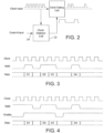
- the divide by N and the divide by M units 12, 14 of Figure 1 are replaced by the clock deletion unit of Figure 2 .
- This comprises a clock gating cell 20 which is positioned between the clock and the clock input to a module.
- This clock gating cell 20 also receives an input from a clock deletion control unit 22.
- This clock deletion control unit 22 also receives the same clock input as the clock gating cell.
- it receives a control input 24 which contains data relating to the required clocking rate, which is to be applied to the module in question.
- the clock deletion control unit 22 In response to the control input 24, the clock deletion control unit 22 generates a series of pulses which get applied to the clock gating cell 20 which in turn cause a clock pulse to be generated at the module.
- the clock deletion control unit of Figure 2 can be set up to delete any arbitrary clock pulses from the master clock signal within a set clock period, and in any arbitrary order to achieve the effective clock frequency required.
- the control input 24 may be modified at any time to change the effective clock frequency as required by the algorithms running on the module.
- each of the divide by N and divide by M units 12, 14 in Figure 1 will be replaced by a clock deletion unit of the type shown in Figure 2 .
- a clock deletion unit for each of the 3 modules in Figure 1 , thereby ensuring that each can be controlled at a varying rate, whereby any module which is not required to perform processes at a particular time may have its clocking pulses removed by a clock deletion unit.
- the two-way handshake protocol used here for illustration is named "valid-enable” which recognise data transfer from one module to the next on the same clock.
- the first example is a non-stalling (known here as 'valid-only') protocol which can be used at an appropriate module interface.
- the signals used in the data transfer are shown in Figure 3 .
- the second line represents a handshake wire 'valid' which, when high indicates that the ⁇ Data' wires have a value to be transferred.
- Valid data to be transferred in shown in Figure 3 as D1, D2, D3 and D4.
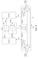
- FIG. 6 A specific embodiment, is illustrated in Figure 6 .
- This is a system in which a coincident clock pulse is forced on both sending and receiving modules when data is ready to be transferred.
- Figure 6 shows two modules which can be clocked at different effective clock rates by respective clock deleter circuits.
- the two modules are modules 1 and module 2.
- Module 1 has a clock deletion control unit 42 which receives clock control 1.
- Module 2 has a clock deletion control unit 44 which receives clock control 2 at its control input.
- Each of the clock deletion control units 42 and 44 provide control signals to their respective clock gating cells 46 via a respective OR gate 48.
- the same clock signal 50 is provided to each clock deletion control unit 42 and 44 and to the two clock gating cells 46.
- Module 1 has to transfer data to module 2. When it is ready to transfer that data it produces a valid signal 52 which is applied to module 2 and which is also applied to the second input of each of the OR gates 48. The effect of this is to cause the output of each OR gate 48 to be enabled irrespective of the outputs of the clock deletion control units.
- the OR gates 48 provides enable signals to their respective clock gating circuits 46 in response to the valid signal 52 of the outputs of the respective clock deletion control units 42 and 44, causing the clock signal 50 to pass through the respective clock gating cell 46 when the output of the respective OR gate 48 is enabled.
- Sophisticated implementations would account for the additional pulses by deleting extra pulses later so the aggregate clock count matches the required rate over a period of time.
- the example protocol used for illustration is known here as a valid-enable transfer which is a two way handshake protocol.
- the protocol is illustrated in Figure 4 .
- the first line shows the clock signal.
- the second line shows the 'valid' signal which originates from the sending module and indicates that the value on the data wires is of interest and to be sent to the receiving module.
- the third line shows the 'enable' signal which originates from the receiving module and indicates that the module is ready to accept data.
- both the valid and enable signals are high, data is transferred from the sending module to the receiving module, shown in Figure 4 as D1, D2, D3 and D4. Without special treatment, this protocol would also suffer from incorrect data transfer if the sending and receiving modules were clocked by different effective clock rates. To avoid this we make use of the handshake signals themselves to ensure that we only attempt to transfer data when there are appropriate clocks on both modules.
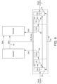
- FIG. 5 A specific embodiment of this alternative arrangement for transferring data between modules in a system on chip is shown with reference to Figure 5 .
- This type of arrangement uses a two way hand shake between modules whereby one processing element can stall back another processing element which wishes to make a data transfer. The effect of this is to ensure that data transfer is only possible when there happens to be coincident clock pulses applied to both sending and receiving modules.
- module 1 has an enable input which is asserted in response to the output of an AND gate 60.
- Module 2 correspondingly has a valid input which is asserted by the output of an AND gate 62.
- the enable input to module 1 permits it to send data to module 2 and the valid input of module 2 permits it to receive data from module 1.
- a first input of the AND gate 60 is an enable signal produced by module 2 when it is in a state in which it is ready to receive data from module 1.
- a first input of the AND gate 62 is a valid output from module 1 which is produced when it is able to send data to module 2.
- the respective second inputs of the AND gates 60 and 62 are provided by a clocking circuit 64.
- the clocking circuit 64 has a clock input 66. This clocking signal is sent to two clock gating circuits of the type described with reference to Figure 2 .
- Module 1 has an clock gating unit comprising a clock deletion control unit 42 receiving a clock control signal 1 at its clock control input. The output of this and the clock signal 66 are provided to its clock gating cell 48 which provides a clock signal to module 1.
- a clock deletion control unit 44 receives a clock control signal at its control input and provides an output to its clock gating cell 48 which in turn provides a clocking signal to module 2.
- the output of the two clock deletion control units 42 and 44 are also provided to a further AND gate 68.
- the output of this forms the second input to the two AND gates 60 and 62.
- the output of AND gate 68 is asserted, thereby permitting data to pass from module 1 to module 2 if module 1 produces a valid signal on its valid output line and module 2 produces an enable signal on its enable line, i.e. when module 1 is ready to send data and module 2 is also ready to receive data.
- data is sent from module 1 to module 2 in response to the clock signals provided at their respective clock inputs by the respective clock gating cells.
- clock control signals may be hard wired to a constant if no control of the clock rate is required. Alternatively, they may be wired to a register so that the clock rate may be controlled by software running on a processor. Alternatively the control signals may be dynamically adjusted by the module whose clock is being controlled, or indeed by any other module responsible for controlling the clocking rates of other modules.
- a metric may be used to provide an indication of whether or not the module being clocked is operating correctly in meeting its real time requirements or whether some adjustment to the clocking speed is required.
- This metric could be generated, for example, by using the fullness of an appropriate FIFO (first in first out buffer) or other hardware that could be constructed to provide an indication of how much the module is over or under performing. This metric can then be fed back to drive directly the clock control signals via suitable scaling and offsetting.
- each of the plurality of modules is clocked with the minimum possible number of clock pulses in any given period of time. It is generally possible to calculate or deduce the minimum clock frequency each module needs to be clocked at to operate its task.
- the clocking may be controlled within a time period to have periods of inaction and periods of higher frequency clocking if the flow of data within the system within which it is operating dictates that this is required.
- the system may have 3 modules that are driven by clock 1, clock 2 and clock 3 or driven from a common master clock. It may have been deduced that the new clock rate required for clock 1, clock 2 and clock 3 are 4, 8 and 3 pulses respectively for every 16 clock periods. A possible configuration for this is shown in Figure 7 with the clock pulses required for clock 1, clock 2 and clock 3. In this example, all the clock pulses occur at the beginning of a 16 period cycle for a respective minimum number of clock cycles to maximise the number of concurrent clock pulses.
- the clock deletion control unit will need to be configured with frame length corresponding to the number of clock periods before a particular cycle restarts. It would also need to know the number of active cycles, i.e. the number of clock periods within a frame for which a clock pulse is generated, and the number of clock periods between output pulses. This would then enable its clock pulse to be altered to ensure optimum flow of data between modules.
Landscapes
- Engineering & Computer Science (AREA)
- Theoretical Computer Science (AREA)
- Physics & Mathematics (AREA)
- General Engineering & Computer Science (AREA)
- General Physics & Mathematics (AREA)
- Computer Networks & Wireless Communication (AREA)
- Signal Processing (AREA)
- Information Transfer Systems (AREA)
- Manipulation Of Pulses (AREA)
- Electric Clocks (AREA)
- Synchronisation In Digital Transmission Systems (AREA)
Description
- This invention relates to clock frequency adjustment for semi-conductor devices and in particular to adjustment of clock frequencies for semi-conductor devices which comprise a plurality of modules which are clocked at different rates, most typically, multiple processing elements provided upon a system on chip (SoC).
- As semi-conductor devices are becoming smaller and smaller, system on chip devices are being produced with more and more different processing elements integrated on the same chip. These processing elements would previously have been provided as separate semi-conductor devices.
- Semi-conductor devices perform their functions in response to clock signals which are provided at one or more inputs to the device and divided and distributed internally to the various processing elements. Where different processing elements form part of the same system and signals are transferred between them, a common clock is normally used. If the various processing elements have differing clock frequency requirements then some consideration needs to be given to how data is transferred between those modules. Data transfer can be kept simple if modules are clocked at integer clock ratios with respect to each other. It is seen, however that if arbitrary clock ratios are required then more expensive and complex synchronisation is required, and this can result in an increased latency penalty on data transfers.
- A typical example SoC device is shown in
Figure 1 . This comprises a plurality of modules, 2, 4, and 6. These may be any combination of central processing units, co-processors, interfaces, arbitration units, or any other circuitry required by the SoC that is driven by a clock. - A master clock signal 8 is provided to phase lock loop (PLL) 10.
Module 1 takes the clock signal from thePLL 10 asclock 1 and performs its functions at this clocking rate. -
Modules 2 and 3 do not need to run as fast as the frequency ofclock 1 which is provided tomodule 1. Therefore, the clock signal to module 2 (clock 2) passes through a divide byN unit 12 and the clock input to module 3 (clock 3) passes through a divide M unit. In this case, N and M are integer amounts. Clockingmodule 2 and module 3 at a lower rates minimises power consumption by these modules. - It will appreciated that provided M and N are kept at simple integer ratios and all three clocks are carefully synchronised, the transfer of data between the modules may be kept relatively simple. For example, it can be arranged that
module 1 will only update its outputs to and read its inputs frommodule 2 every N clock cycles. Similarly,module 1 will only transfer data to and read its inputs from module 3 once every M clock cycles. - If other ratios of M and N are used (i.e. non integer values) the transfer of data between modules can become more complex and it can become necessary to insert a first in first out buffer (FIFO) or some
special synchronisation logic 16 as shown betweenmodules 2 and 3 inFigure 1 . - Some processing systems will have processing requirements which are dynamically variable. Thus, a circuit such as
Figure 1 could usemodule 1 to perform a significant amount of processing beforemodule 2 performed any processing at all. Ifmodule 2 were clocked at the same rate asmodule 1 then there would be unnecessary power consumption bymodule 2 in the first stage of the process. Ifmodule 2 is operated at a lower clock frequency then the second part of the process would be performed more slowly than the first part. Dynamic variation of clock speed is desirable to provide optimal processing rates in such situations but difficult to achieve, especially when there is a requirement to transfer data between modules running at different clock frequencies. -
US 2005/055592 A1 describes dynamically managing power consumption by providing clock input to a device only when communications include the particular device identifier. A common clock signal can be provided to the module of each subsystem. Each of the subsystem modules may operate at a different frequency. -
WO0212988 -
EP0428771 describes a bidirectional data transfer device for the data interface of two data-exchanging cells which in each case contain a data source and a data sink. - Preferred embodiments of the present invention provide devices and methods according to the independent claims in which any module's effective clock rate can be fine tuned. This is achieved by providing synchronised clock signals to each module in an SoC where each clock signal is being run at the same basic rate. In order to reduce the clocking rate for a module, a clock gating cell is provided in the clock input line. This is under the control of a clock deletion control unit which controls the clock gating cell to delete clock pulses which are not required in order to achieve an apparent lower clock rate, or a variable clock rate.
- Preferably the clock deletion control unit can be set up to delete any arbitrary number of clock pulses from a master clock signal in a set period to achieve the effective clock frequency required. Furthermore, the clock deletion control unit can be modified to regulate the effective clock frequency as required by algorithms running on the processing elements or modules. This control may be via a register setting, possibly modifiable by software running on the SoC, or alternatively it can be dynamically set to an optimum value via a metric generated within the algorithms running within the module to which the clock pulses being supplied.
- Each module within an SoC may have its own dedicated clock deletion control unit and clock gating cell so that each may be run at different clocking rates. Safe data transfer between modules running at different clocking rates is handled by either forcing a clock pulse on the sending and receiving modules when there is data to be transferred, or making use of an existing two way handshake to deliberately stall the transfer of data until appropriate clock pulses happen to occur on both the sending and receiving modules. A combination of these methods may also be used.
- An embodiment of the invention will now be described in more detail by way of example with reference to the accompanying drawings in which:
-
Figure 1 is the prior art system referred to above; -
Figure 2 shows a clock gating cell and clock deletion control unit in accordance with an embodiment of the invention; -
Figure 3 shows the timing wave forms of a non-stalling (valid only) protocol; -
Figure 4 shows the timing wave form for data transfer between modules with a specific two way handshake. (valid-enable protocol); -
Figure 5 shows an embodiment of the invention in which a two-way handshake protocol is modified to ensure correct data transfer; -
Figure 6 shows an embodiment of the invention in which clock pulses are forced onto modules to ensure correct data transfer; -
Figure 7 shows one arrangement of the clocking configuration for use with an embodiment of; and, -
Figure 8 shows an optimised clocking configuration for transfer betweenmodules Figure 6 - In a preferred embodiment of the invention, the divide by N and the divide by
M units Figure 1 are replaced by the clock deletion unit ofFigure 2 . This comprises a clock gating cell 20 which is positioned between the clock and the clock input to a module. This clock gating cell 20 also receives an input from a clockdeletion control unit 22. This clockdeletion control unit 22 also receives the same clock input as the clock gating cell. In addition, it receives acontrol input 24 which contains data relating to the required clocking rate, which is to be applied to the module in question. In response to thecontrol input 24, the clockdeletion control unit 22 generates a series of pulses which get applied to the clock gating cell 20 which in turn cause a clock pulse to be generated at the module. - Thus, the clock deletion control unit of
Figure 2 can be set up to delete any arbitrary clock pulses from the master clock signal within a set clock period, and in any arbitrary order to achieve the effective clock frequency required. Furthermore, thecontrol input 24 may be modified at any time to change the effective clock frequency as required by the algorithms running on the module. - In a preferred embodiment, each of the divide by N and divide by
M units Figure 1 will be replaced by a clock deletion unit of the type shown inFigure 2 . Indeed, it may be preferable to provide a clock deletion unit for each of the 3 modules inFigure 1 , thereby ensuring that each can be controlled at a varying rate, whereby any module which is not required to perform processes at a particular time may have its clocking pulses removed by a clock deletion unit. - When an SOC is in operation, it will from time to time be necessary to transfer data between two or more modules. When this is necessary, it must be ensured that the modules are clocked at the appropriate times. This can be achieved in a number of ways including the following;
- 1. by forcing a clock pulse on both modules at the appropriate times when there is valid data to transfer, or,
- 2. by making use of existing two-way handshake wires to naturally control the data flow from one module to the other where the transfer is recognised at both sides. The use of the handshake signal is subverted to allow only data to flow on the occasions when there happens to be a coincident clock pulse on both modules
- The two-way handshake protocol used here for illustration is named "valid-enable" which recognise data transfer from one module to the next on the same clock.
- It is also possible to accommodate two-way handshake protocols which recognise transfer on different clocks. These require different specific logic designed around the interface protocol for the data transfer.
- We will now describe examples of the two methods of transferring data between modules which may be used in embodiments of the present invention. In particular, we show methods for transferring data between modules which are clocked at different effective rates. Both techniques may be used on the same SoC between any number of modules running at any number of effective clock rates. The best choice for the method selected will depend on whether or not a one or two way hand shake protocol is available. It may also depend on the expected characteristics of the data transfer by the selected interface.
- The first example is a non-stalling (known here as 'valid-only') protocol which can be used at an appropriate module interface. The signals used in the data transfer are shown in
Figure 3 . As can be seen, there is a clock signal shown on the top line. The second line represents a handshake wire 'valid' which, when high indicates that the `Data' wires have a value to be transferred. Valid data to be transferred in shown inFigure 3 as D1, D2, D3 and D4. - In the case where both modules are driven by the same clock, the 'valid-only' protocol works without problem. If however the modules are driven at different rates with different clock control settings there is potential for valid data to get lost, or for single words of valid data to get mis-interpreted as multiple words. To avoid this happening we take the valid signal and combine it with the clock gating signals from each of the clock control units to force a clock pulse on each module whenever there is valid data to be transferred.
- A specific embodiment, is illustrated in
Figure 6 . This is a system in which a coincident clock pulse is forced on both sending and receiving modules when data is ready to be transferred.Figure 6 shows two modules which can be clocked at different effective clock rates by respective clock deleter circuits. The two modules aremodules 1 andmodule 2.Module 1 has a clockdeletion control unit 42 which receivesclock control 1.Module 2 has a clockdeletion control unit 44 which receivesclock control 2 at its control input. - Each of the clock
deletion control units clock gating cells 46 via a respective ORgate 48. Thesame clock signal 50 is provided to each clockdeletion control unit clock gating cells 46. -
Module 1 has to transfer data tomodule 2. When it is ready to transfer that data it produces avalid signal 52 which is applied tomodule 2 and which is also applied to the second input of each of theOR gates 48. The effect of this is to cause the output of eachOR gate 48 to be enabled irrespective of the outputs of the clock deletion control units. - Thus, the OR
gates 48 provides enable signals to their respectiveclock gating circuits 46 in response to thevalid signal 52 of the outputs of the respective clockdeletion control units clock signal 50 to pass through the respectiveclock gating cell 46 when the output of the respective ORgate 48 is enabled. - Sophisticated implementations would account for the additional pulses by deleting extra pulses later so the aggregate clock count matches the required rate over a period of time.
- When a handshake mechanism is present which allows the receiving module to stall data transfer an alternative mechanism is employed to ensure correct data transfer when the modules are clocked at different effective rates. The example protocol used for illustration is known here as a valid-enable transfer which is a two way handshake protocol. The protocol is illustrated in
Figure 4 . The first line shows the clock signal. The second line shows the 'valid' signal which originates from the sending module and indicates that the value on the data wires is of interest and to be sent to the receiving module. The third line shows the 'enable' signal which originates from the receiving module and indicates that the module is ready to accept data. When both the valid and enable signals are high, data is transferred from the sending module to the receiving module, shown inFigure 4 as D1, D2, D3 and D4. Without special treatment, this protocol would also suffer from incorrect data transfer if the sending and receiving modules were clocked by different effective clock rates. To avoid this we make use of the handshake signals themselves to ensure that we only attempt to transfer data when there are appropriate clocks on both modules. - A specific embodiment of this alternative arrangement for transferring data between modules in a system on chip is shown with reference to
Figure 5 . This type of arrangement uses a two way hand shake between modules whereby one processing element can stall back another processing element which wishes to make a data transfer. The effect of this is to ensure that data transfer is only possible when there happens to be coincident clock pulses applied to both sending and receiving modules. - In this arrangement,
module 1 has an enable input which is asserted in response to the output of an ANDgate 60.Module 2 correspondingly has a valid input which is asserted by the output of an ANDgate 62. The enable input tomodule 1 permits it to send data tomodule 2 and the valid input ofmodule 2 permits it to receive data frommodule 1. - A first input of the AND
gate 60 is an enable signal produced bymodule 2 when it is in a state in which it is ready to receive data frommodule 1. A first input of the ANDgate 62 is a valid output frommodule 1 which is produced when it is able to send data tomodule 2. The respective second inputs of the ANDgates clocking circuit 64. - The
clocking circuit 64 has aclock input 66. This clocking signal is sent to two clock gating circuits of the type described with reference toFigure 2 .Module 1 has an clock gating unit comprising a clockdeletion control unit 42 receiving aclock control signal 1 at its clock control input. The output of this and theclock signal 66 are provided to itsclock gating cell 48 which provides a clock signal tomodule 1. - Correspondingly, for
module 2, a clockdeletion control unit 44 receives a clock control signal at its control input and provides an output to itsclock gating cell 48 which in turn provides a clocking signal tomodule 2. - The output of the two clock
deletion control units gate 68. The output of this forms the second input to the two ANDgates deletion control units gate 68 is asserted, thereby permitting data to pass frommodule 1 tomodule 2 ifmodule 1 produces a valid signal on its valid output line andmodule 2 produces an enable signal on its enable line, i.e. whenmodule 1 is ready to send data andmodule 2 is also ready to receive data. When this happens, data is sent frommodule 1 tomodule 2 in response to the clock signals provided at their respective clock inputs by the respective clock gating cells. - This arrangement works most effectively when the clock deletion circuits have a maximum number of coincident clock pulses between them, thereby minimising the chance of one module being unnecessarily stalled whilst waiting for data for transfer to or from the other. A line is shown between the two clock deletion control units in
Figure 6 and this represents linkage between the two clock control inputs to provide some synchronization and thereby ensure maximum number of coincident clock pulses. - In these embodiments of the invention, clock control signals may be hard wired to a constant if no control of the clock rate is required. Alternatively, they may be wired to a register so that the clock rate may be controlled by software running on a processor. Alternatively the control signals may be dynamically adjusted by the module whose clock is being controlled, or indeed by any other module responsible for controlling the clocking rates of other modules.
- In the dynamic control case, a metric may be used to provide an indication of whether or not the module being clocked is operating correctly in meeting its real time requirements or whether some adjustment to the clocking speed is required. This metric could be generated, for example, by using the fullness of an appropriate FIFO (first in first out buffer) or other hardware that could be constructed to provide an indication of how much the module is over or under performing. This metric can then be fed back to drive directly the clock control signals via suitable scaling and offsetting.
- Preferably, each of the plurality of modules is clocked with the minimum possible number of clock pulses in any given period of time. It is generally possible to calculate or deduce the minimum clock frequency each module needs to be clocked at to operate its task. The clocking may be controlled within a time period to have periods of inaction and periods of higher frequency clocking if the flow of data within the system within which it is operating dictates that this is required.
- It is preferable to maximise the number of concurrent clock pulses between modules so that data is more likely to be transferred between modules as and when it becomes available, rather than having to wait and possibly slow down the system. For example the system may have 3 modules that are driven by
clock 1,clock 2 and clock 3 or driven from a common master clock. It may have been deduced that the new clock rate required forclock 1,clock 2 and clock 3 are 4, 8 and 3 pulses respectively for every 16 clock periods. A possible configuration for this is shown inFigure 7 with the clock pulses required forclock 1,clock 2 and clock 3. In this example, all the clock pulses occur at the beginning of a 16 period cycle for a respective minimum number of clock cycles to maximise the number of concurrent clock pulses. - It is also desirable to take account of the expected rates at which modules produce or receive data and modify the clocking pattern appropriately. For example, if
module 1 delivers data tomodule 2 on average one word every 2 clock pulses,module 2needs 4 clock pulses to deal with each word it receives, the arrangement of clock pulses shown inFigure 7 will not be appropriate. For this situation, a FIFO buffer between the modules would be required to maintain smooth data flow. Alternatively, this requirement can be eliminated by arranging the waveforms differently as shown inFigure 8 . In this, the clock pulses applied toclock 1 are spread to enablemodule 2 to process the data as it receives it frommodule 1. - To produce waveforms with characteristics such as shown in
Figure 8 , the clock deletion control unit will need to be configured with frame length corresponding to the number of clock periods before a particular cycle restarts. It would also need to know the number of active cycles, i.e. the number of clock periods within a frame for which a clock pulse is generated, and the number of clock periods between output pulses. This would then enable its clock pulse to be altered to ensure optimum flow of data between modules.
Claims (14)
- Apparatus for transferring data between a first module (Modulel) and a second module (Module2); the apparatus comprising:I) a first AND gate (62) comprising respective first and second inputs and an output; wherein:the first input of the first AND gate (62) is a valid output from the first module (Modulel) produced when the first module (Modulel) is able to send data to the second module (Module2);the output is a valid input to the second module (Module2);II) a second AND gate (60) comprising respective first and second inputs and an output;
wherein:the first input of the second AND gate (60) is an enable signal produced by the second module (Module2) when the second module (Module2) is in a state in which it is ready to receive data from the first module (Module1);the output is an enable input to the first module (Module1);III) a third AND gate (68) for outputting a signal to the respective second inputs of the first AND gate (62) and the second AND gate (60);IV) a first clock deletion control unit (42);V) a first clock gating cell (48);VI) a second clock deletion control unit (44);VII) a second clock gating cell (48);
wherein:A) the first clock deletion control unit (42) is configured to:receive:a first clock control signal (1);a clock input signal (66); and,output a signal for inputting to the first clock gating cell (48) and the third AND gate (68);B) the first clock gating cell (48) is configured to:receive:the output from the first clock deletion control unit (42);the clock input signal (66);output a clock signal to the first module (Module1);C) the second clock deletion control unit (44) is configured to:receive:a second clock control signal (2);the clock input signal (66); and,output a signal for inputting to the second clock gating cell (48) and the third AND gate (68);D) the second clock gating cell (48) is configured to:receive:the output from the second clock deletion control unit (44);the clock input signal (66);output a clock signal to the second module (Module2). - An apparatus as claimed in claim 1 wherein the first and second clock deletion control units are configured to delete any arbitrary number of clock pulses from the clock input signal (66) in a set period to achieve an effective clock frequency required.
- An apparatus as claimed in claims 1 or 2 wherein the apparatus is a system on chip (SoC).
- An apparatus as claimed in any preceding claim wherein the second module (module2) stalls the making of a data transfer by the first module (module1).
- A method for transferring data between a first module (Modulel) and a second module (Module2) using:a first AND gate (62);a second AND gate (60);a third AND gate (68);the method comprising:I) in any order:i) receiving a first clock control signal (1) and a clock input signal (66) at a first clock deletion control unit (42);
outputting a signal from the first clock deletion control unit (42) for inputting to a first clock gating cell (48) and the third AND gate (68);ii) receiving a second clock control signal (2) and the clock input signal (66) at a second clock deletion control unit (44);
outputting a signal from the second clock deletion control unit (44) for inputting to a second clock gating cell (48) and the third AND gate (68);II) in any order:iii) receiving the clock input signal (66) and the output signal from the first clock deletion control unit (42) at the first clock gating cell (48); and,
outputting a clock signal to the first module (Module1);iv) receiving the clock input signal (66) and the output signal from the second clock deletion control unit (44) at the second clock gating cell (48);
outputting a clock signal to the second module (Module2);III) outputting a signal from the third AND gate (68) to the first AND gate (62) and the second AND gate (60);IV) outputting from the first module (Module1), when the first module (Modulel) is able to send data to the second module (Module2), a valid output to the first AND gate (62);V) outputting from the first AND gate (62), upon receiving the valid output and the output signal from the third AND gate (68), a valid input to the second module (Module2);VI) outputting from the second module (Module2), when second module (Module2) is ready to receive data from the first module (Module1), an enable output to the second AND gate (62);VII) outputting from the second AND gate (60), upon receiving the enable output and the output signal from the third AND gate (68), an enable input to the first module (Module1);VIII) transferring data from the first module (Modulel) to the second module (Module2) upon the first module (Modulel) receiving the enable input. - A method as claimed in claim 5 wherein the first and second clock deletion control units are configured to delete any arbitrary number of clock pulses from the clock input signal (66) in a set period to achieve an effective clock frequency required.
- A method as claimed in claims 5 or 6 wherein apparatus such that the second module stalls the making of a data transfer by module 1.
- Apparatus for transferring data between a first module (Modulel) and a second module (Module2) upon a valid signal (52) output from the first module (Modulel) to the second module (Module2); the apparatus comprising:I) a first clock deletion control unit (42);II) a first clock gating cell (46);III) a first OR gateIV) a second clock deletion control unit (44);V) a second clock gating cell (46);V) a second OR gate;wherein:A) the first clock deletion control unit (42) is configured to:receive:a first clock control signal (1);a clock input signal (50); and,output a signal for inputting to the first clock gating cell (46) via the first OR gate;B) the first clock gating cell (46) is configured to:receive:the output from the first clock deletion control unit (42) via the first OR gate;the clock input signal (50);output a clock signal to the first module (Module1);C) the second clock deletion control unit (44) is configured to:receive:a second clock control signal (2);the clock input signal (50); and,output a signal for inputting to the second clock gating cell (46) via the second OR gate;D) the second clock gating cell (46) is configured to:receive:the output from the second clock deletion control unit (44) via the second OR gate;the clock input signal (50);output a clock signal to the second module (Module2);E) the first and second OR gates are configured to provided enable signals to their respective clock gating circuits (46) in response to the valid signal (52), causing the clock signal (50) to pass through the respective clock gating cell (46).
- An apparatus as claimed in claim 8 wherein the first and second clock deletion control units are configured to delete any arbitrary number of clock pulses from the clock input signal (50) in a set period to achieve an effective clock frequency required.
- An apparatus as claimed in claims 8 or 9 wherein the apparatus is a system on chip (SoC).
- An apparatus as claimed in claims 8, 9 or 10 wherein a coincident clock pulse is forced on both first and second modules when data is ready to be transferred.
- A method for transferring data between a first module (Modulel) and a second module (Module2) upon a valid signal (52) output from the first module (Modulel) to the second module (Module2);
the method comprising:I) in any order:v) receiving a first clock control signal (1) and a clock input signal (50) at a first clock deletion control unit (42);
outputting a signal from the first clock deletion control unit (42) for inputting to a first clock gating cell (46) via a first OR gate;vi) receiving a second clock control signal (2) and the clock input signal (50) at a second clock deletion control unit (44);
outputting a signal from the second clock deletion control unit (44) for inputting to a second clock gating cell (46) via a second OR gate;II) in any order:vii) receiving, at the first clock gating cell (46),the output signal of the first clock deletion control unit (42) via the first OR gate; and,the clock input signal (50); and,outputting a clock signal to the first module (Module1);viii) receiving, at the second clock gating cell (46),the output signal from the second clock deletion control unit (44) via the second OR gate; and,the clock input signal (50);outputting a clock signal to the second module (Module2);III) transferring data from the first module (Modulel) to the second module (Module2), wherein the first and second OR gates are configured to provided enable signals to their respective clock gating circuits (46) in response to the valid signal (52), causing the clock signal (50) to pass through the respective clock gating cell (46). - A method as claimed in claim 12 wherein the first and second clock deletion control units are configured to delete any arbitrary number of clock pulses from the clock input signal (50) in a set period to achieve an effective clock frequency required.
- A method as claimed in claims 12 or 13 wherein a coincident clock pulse is forced on both first and second modules when data is ready to be transferred.
Applications Claiming Priority (3)
| Application Number | Priority Date | Filing Date | Title |
|---|---|---|---|
| GB0712788A GB2450564B (en) | 2007-06-29 | 2007-06-29 | Clock frequency adjustment for semi-conductor devices |
| EP08775815.7A EP2171557B1 (en) | 2007-06-29 | 2008-06-30 | Clock frequency adjustment for semi-conductor devices |
| PCT/GB2008/002265 WO2009004330A2 (en) | 2007-06-29 | 2008-06-30 | Clock frequency adjustment for semi-conductor devices |
Related Parent Applications (2)
| Application Number | Title | Priority Date | Filing Date |
|---|---|---|---|
| EP08775815.7A Division EP2171557B1 (en) | 2007-06-29 | 2008-06-30 | Clock frequency adjustment for semi-conductor devices |
| EP08775815.7A Division-Into EP2171557B1 (en) | 2007-06-29 | 2008-06-30 | Clock frequency adjustment for semi-conductor devices |
Publications (2)
| Publication Number | Publication Date |
|---|---|
| EP3147751A1 EP3147751A1 (en) | 2017-03-29 |
| EP3147751B1 true EP3147751B1 (en) | 2023-06-07 |
Family
ID=38421062
Family Applications (2)
| Application Number | Title | Priority Date | Filing Date |
|---|---|---|---|
| EP08775815.7A Active EP2171557B1 (en) | 2007-06-29 | 2008-06-30 | Clock frequency adjustment for semi-conductor devices |
| EP16197178.3A Active EP3147751B1 (en) | 2007-06-29 | 2008-06-30 | Clock frequency adjustment for semi-conductor devices |
Family Applications Before (1)
| Application Number | Title | Priority Date | Filing Date |
|---|---|---|---|
| EP08775815.7A Active EP2171557B1 (en) | 2007-06-29 | 2008-06-30 | Clock frequency adjustment for semi-conductor devices |
Country Status (5)
| Country | Link |
|---|---|
| US (5) | US8595541B2 (en) |
| EP (2) | EP2171557B1 (en) |
| JP (1) | JP5401453B2 (en) |
| GB (1) | GB2450564B (en) |
| WO (1) | WO2009004330A2 (en) |
Families Citing this family (15)
| Publication number | Priority date | Publication date | Assignee | Title |
|---|---|---|---|---|
| GB2450564B (en) | 2007-06-29 | 2011-03-02 | Imagination Tech Ltd | Clock frequency adjustment for semi-conductor devices |
| CN102193581B (en) * | 2010-02-12 | 2015-06-17 | 英特尔移动通信技术德累斯顿有限公司 | Circuitry system and method for connecting synchronous clock domains of the circuitry system |
| US9214924B2 (en) * | 2011-03-25 | 2015-12-15 | Freescale Semiconductor, Inc. | Integrated circuit and method for reducing an impact of electrical stress in an integrated circuit |
| WO2013018218A1 (en) * | 2011-08-03 | 2013-02-07 | 富士通株式会社 | Synchronization control device, computational processing device, parallel computer system and control method for synchronization control device |
| US20150149800A1 (en) * | 2013-11-27 | 2015-05-28 | Alexander Gendler | Performing an operating frequency change using a dynamic clock control technique |
| FR3018970B1 (en) * | 2014-03-20 | 2016-03-25 | Inside Secure | METHOD AND CIRCUIT FOR ADJUSTING THE FREQUENCY OF A CLOCK SIGNAL |
| US9582026B2 (en) | 2014-09-30 | 2017-02-28 | Samsung Electronics Co., Ltd. | System-on-chip to support full handshake and mobile device having the same |
| KR102290984B1 (en) * | 2014-09-30 | 2021-08-18 | 삼성전자주식회사 | System-on-chip to support full handshake and mobile device having the same |
| JP6441166B2 (en) * | 2015-05-15 | 2018-12-19 | ルネサスエレクトロニクス株式会社 | Semiconductor device |
| US9986036B2 (en) * | 2015-07-16 | 2018-05-29 | Ge Aviation Systems, Llc | Apparatus and method of operating a system |
| US20190050020A1 (en) * | 2017-08-10 | 2019-02-14 | Qualcomm Incorporated | Clock Signal Staggering with Clock Frequency Adjustment |
| KR102781500B1 (en) * | 2018-02-09 | 2025-03-17 | 삼성전자주식회사 | System on chip performing clock training and computing system comprising the same |
| US11981587B2 (en) * | 2020-01-30 | 2024-05-14 | Michael Schelch | Disinfection device and method for performing disinfection cycles |
| US12360552B2 (en) * | 2021-06-16 | 2025-07-15 | Avago Technologies International Sales Pte. Limited | Synchronization of devices with a gapped reference clock |
| US20260003389A1 (en) * | 2024-06-28 | 2026-01-01 | Qualcomm Incorporated | Modularized clock conditioning |
Citations (1)
| Publication number | Priority date | Publication date | Assignee | Title |
|---|---|---|---|---|
| WO2002012988A1 (en) * | 2000-08-04 | 2002-02-14 | Insilicon Corporation | Method and system for providing gated clock signal to a csr block |
Family Cites Families (67)
| Publication number | Priority date | Publication date | Assignee | Title |
|---|---|---|---|---|
| EP0428771B1 (en) | 1989-11-21 | 1995-02-01 | Deutsche ITT Industries GmbH | Bidirectional data transfer device |
| JPH0816857B2 (en) * | 1990-07-20 | 1996-02-21 | 富士通株式会社 | Clock controller |
| US5826068A (en) * | 1994-11-09 | 1998-10-20 | Adaptec, Inc. | Integrated circuit with a serial port having only one pin |
| JP2908739B2 (en) * | 1994-12-16 | 1999-06-21 | インターナショナル・ビジネス・マシーンズ・コーポレイション | System and method for monitoring a CPU in a multiprocessor system |
| JP3466755B2 (en) * | 1995-03-08 | 2003-11-17 | キヤノン株式会社 | Electronics |
| US5777500A (en) * | 1996-01-16 | 1998-07-07 | Cyrix Corporation | Multiple clock source generation with independently adjustable duty cycles |
| US5884100A (en) * | 1996-06-06 | 1999-03-16 | Sun Microsystems, Inc. | Low-latency, high-throughput, integrated cache coherent I/O system for a single-chip processor |
| JP3000961B2 (en) * | 1997-06-06 | 2000-01-17 | 日本電気株式会社 | Semiconductor integrated circuit |
| JP3209943B2 (en) * | 1997-06-13 | 2001-09-17 | 沖電気工業株式会社 | Voltage control delay circuit, direct phase control type voltage controlled oscillator, clock / data recovery circuit, and clock / data recovery device |
| US6115823A (en) * | 1997-06-17 | 2000-09-05 | Amphus, Inc. | System and method for task performance based dynamic distributed power management in a computer system and design method therefor |
| US5995570A (en) * | 1997-06-27 | 1999-11-30 | International Business Machines Corporation | Recovering a clock signal in a multimedia network using time stamps |
| US5963068A (en) * | 1997-07-28 | 1999-10-05 | Motorola Inc. | Fast start-up processor clock generation method and system |
| CA2220622C (en) * | 1997-11-03 | 2004-03-30 | Aubin P. J. Roy | Method and circuit for built in self test of phase locked loops |
| US6049236A (en) * | 1997-11-17 | 2000-04-11 | Lucent Technologies Inc. | Divide-by-one or divide-by-two qualified clock driver with glitch-free transitions between operating frequencies |
| US6202164B1 (en) * | 1998-07-02 | 2001-03-13 | Advanced Micro Devices, Inc. | Data rate synchronization by frame rate adjustment |
| US6247082B1 (en) * | 1998-11-03 | 2001-06-12 | 3Com Corporation | Method and circuit for providing handshaking to transact information across multiple clock domains |
| US6453426B1 (en) * | 1999-03-26 | 2002-09-17 | Microsoft Corporation | Separately storing core boot data and cluster configuration data in a server cluster |
| US6529571B1 (en) * | 1999-09-28 | 2003-03-04 | National Semiconductor Corporation | Method and apparatus for equalizing propagation delay |
| US6918540B2 (en) * | 2000-04-18 | 2005-07-19 | Metrologic Instruments, Inc. | Bioptical point-of-sale (pos) scanning system employing dual polygon-based laser scanning platforms disposed beneath horizontal and vertical scanning windows for 360° omni-directional bar code scanning |
| US6715093B1 (en) * | 2000-04-28 | 2004-03-30 | Hewlett-Packard Development Company, L.P. | Method for triggering an asynchronous event by creating a lowest common denominator clock |
| US6735712B1 (en) * | 2000-09-08 | 2004-05-11 | Intel Corporation | Dynamically configurable clocking scheme for demand based resource sharing with multiple clock crossing domains |
| US6920572B2 (en) * | 2000-11-15 | 2005-07-19 | Texas Instruments Incorporated | Unanimous voting for disabling of shared component clocking in a multicore DSP device |
| JP2002171140A (en) * | 2000-12-01 | 2002-06-14 | Mitsubishi Electric Corp | Audio signal amplification output circuit |
| US6456146B1 (en) * | 2000-12-28 | 2002-09-24 | Intel Corp. | System and method for multiplexing clocking signals |
| US7039146B2 (en) * | 2001-01-16 | 2006-05-02 | Advanced Micro Devices, Inc. | Method and interface for glitch-free clock switching |
| GB2372847B (en) * | 2001-02-19 | 2004-12-29 | Imagination Tech Ltd | Control of priority and instruction rates on a multithreaded processor |
| KR20020072049A (en) * | 2001-03-08 | 2002-09-14 | 엘지전자 주식회사 | Apparatus for removal glitch |
| DE10121821B4 (en) * | 2001-05-04 | 2004-04-08 | Infineon Technologies Ag | Frequency control circuit |
| US6982573B2 (en) * | 2001-05-30 | 2006-01-03 | Stmicroelectronics Limited | Switchable clock source |
| US6938176B1 (en) * | 2001-10-05 | 2005-08-30 | Nvidia Corporation | Method and apparatus for power management of graphics processors and subsystems that allow the subsystems to respond to accesses when subsystems are idle |
| US7010714B1 (en) * | 2001-10-17 | 2006-03-07 | Lsi Logic Corporation | Prescaler architecture capable of non integer division |
| JP3956768B2 (en) * | 2002-05-14 | 2007-08-08 | ソニー株式会社 | Clock generation circuit |
| US7076681B2 (en) * | 2002-07-02 | 2006-07-11 | International Business Machines Corporation | Processor with demand-driven clock throttling power reduction |
| US7051227B2 (en) * | 2002-09-30 | 2006-05-23 | Intel Corporation | Method and apparatus for reducing clock frequency during low workload periods |
| US7774627B2 (en) * | 2002-10-03 | 2010-08-10 | Via Technologies, Inc. | Microprocessor capable of dynamically increasing its performance in response to varying operating temperature |
| US7290156B2 (en) * | 2003-12-17 | 2007-10-30 | Via Technologies, Inc. | Frequency-voltage mechanism for microprocessor power management |
| US6856184B2 (en) * | 2003-01-15 | 2005-02-15 | Agilent Technologies, Inc | Clock divider circuit |
| US7237216B2 (en) * | 2003-02-21 | 2007-06-26 | Infineon Technologies Ag | Clock gating approach to accommodate infrequent additional processing latencies |
| JP2004326222A (en) * | 2003-04-22 | 2004-11-18 | Renesas Technology Corp | Data processing system |
| TWI221369B (en) * | 2003-04-29 | 2004-09-21 | Via Tech Inc | Device and method for adjusting the frequency of the timing signal |
| JP2004348573A (en) * | 2003-05-23 | 2004-12-09 | Renesas Technology Corp | Clock generation circuit and system including it |
| US7945803B2 (en) * | 2003-06-18 | 2011-05-17 | Nethra Imaging, Inc. | Clock generation for multiple clock domains |
| JP4136822B2 (en) * | 2003-07-31 | 2008-08-20 | 富士通株式会社 | Semiconductor integrated circuit device, clock control method, and data transfer control method |
| JP3870942B2 (en) * | 2003-10-20 | 2007-01-24 | ソニー株式会社 | Data transmission system and data transmission apparatus |
| US7176738B1 (en) * | 2003-11-20 | 2007-02-13 | Integrated Device Technology, Inc. | Method and apparatus for clock generation |
| US20060195714A1 (en) * | 2003-12-26 | 2006-08-31 | Sony Corporation | Clock control device, microprocessor, electronic device, clock control method, and clock control program |
| US7151399B2 (en) * | 2004-02-02 | 2006-12-19 | Toshiba America Electronic Components, Inc. | System and method for generating multiple clock signals |
| US7376152B2 (en) * | 2004-03-30 | 2008-05-20 | Via Telecom Co., Ltd. | Method and/or architecture implemented in hardware for the adjustment of messages with indeterministic length |
| JP4095576B2 (en) * | 2004-05-17 | 2008-06-04 | 株式会社東芝 | General-purpose logic circuit device using programmable logic circuit |
| US7500123B2 (en) * | 2004-06-28 | 2009-03-03 | Ati Technologies Ulc | Apparatus and method for reducing power consumption in a graphics processing device |
| US7219252B1 (en) * | 2004-07-09 | 2007-05-15 | Cypress Semiconductor Corp. | Apparatus and method for dynamic overclocking |
| JP4808414B2 (en) * | 2005-01-31 | 2011-11-02 | 富士通株式会社 | Computer system and memory system |
| US20060221936A1 (en) * | 2005-03-31 | 2006-10-05 | Rauchwerk Michael D | Timing recovery for modem transmission on IP networks |
| US7401243B2 (en) * | 2005-06-21 | 2008-07-15 | Dell Products L.P. | Demand-based dynamic clock control for transaction processors |
| JP4799137B2 (en) * | 2005-11-15 | 2011-10-26 | キヤノン株式会社 | Bus system |
| US7415645B2 (en) * | 2005-07-28 | 2008-08-19 | International Business Machines Corporation | Method and apparatus for soft-error immune and self-correcting latches |
| US20070074054A1 (en) * | 2005-09-27 | 2007-03-29 | Chieh Lim S | Clock gated pipeline stages |
| US7472299B2 (en) * | 2005-09-30 | 2008-12-30 | Intel Corporation | Low power arbiters in interconnection routers |
| US7411429B2 (en) * | 2005-10-28 | 2008-08-12 | Silicon Integrated Systems Corp. | System and method for clock switching |
| TW200731078A (en) * | 2005-12-27 | 2007-08-16 | Via Tech Inc | Computer system with clock-controlled wait states |
| US7478214B2 (en) * | 2006-01-04 | 2009-01-13 | Intel Corporation | Clock-gated random access memory |
| US7339405B2 (en) * | 2006-02-02 | 2008-03-04 | Mediatek, Inc. | Clock rate adjustment apparatus and method for adjusting clock rate |
| US20080012605A1 (en) * | 2006-07-12 | 2008-01-17 | Eastman Kodak Company | Glitch-free clock switcher |
| US7725754B1 (en) * | 2006-08-08 | 2010-05-25 | Xilinx, Inc. | Dual clock interface for an integrated circuit |
| US7752480B2 (en) * | 2006-08-18 | 2010-07-06 | International Business Machines Corporation | System and method for switching digital circuit clock net driver without losing clock pulses |
| US7737752B2 (en) * | 2007-05-17 | 2010-06-15 | Globalfoundries Inc | Techniques for integrated circuit clock management |
| GB2450564B (en) | 2007-06-29 | 2011-03-02 | Imagination Tech Ltd | Clock frequency adjustment for semi-conductor devices |
-
2007
- 2007-06-29 GB GB0712788A patent/GB2450564B/en active Active
-
2008
- 2008-06-27 US US12/215,691 patent/US8595541B2/en active Active
- 2008-06-30 JP JP2010514118A patent/JP5401453B2/en not_active Expired - Fee Related
- 2008-06-30 EP EP08775815.7A patent/EP2171557B1/en active Active
- 2008-06-30 EP EP16197178.3A patent/EP3147751B1/en active Active
- 2008-06-30 WO PCT/GB2008/002265 patent/WO2009004330A2/en not_active Ceased
-
2013
- 2013-11-18 US US14/082,391 patent/US9473290B2/en active Active
-
2016
- 2016-09-19 US US15/269,122 patent/US10419198B2/en active Active
-
2019
- 2019-08-05 US US16/531,581 patent/US11509450B2/en active Active
-
2022
- 2022-10-31 US US17/977,456 patent/US11831745B2/en active Active
Patent Citations (1)
| Publication number | Priority date | Publication date | Assignee | Title |
|---|---|---|---|---|
| WO2002012988A1 (en) * | 2000-08-04 | 2002-02-14 | Insilicon Corporation | Method and system for providing gated clock signal to a csr block |
Also Published As
| Publication number | Publication date |
|---|---|
| JP2010532124A (en) | 2010-09-30 |
| EP2171557A2 (en) | 2010-04-07 |
| US11831745B2 (en) | 2023-11-28 |
| WO2009004330A3 (en) | 2009-06-11 |
| US20200014524A1 (en) | 2020-01-09 |
| US20140140457A1 (en) | 2014-05-22 |
| US20170005779A1 (en) | 2017-01-05 |
| GB2450564A (en) | 2008-12-31 |
| GB0712788D0 (en) | 2007-08-08 |
| US9473290B2 (en) | 2016-10-18 |
| GB2450564B (en) | 2011-03-02 |
| US11509450B2 (en) | 2022-11-22 |
| EP2171557B1 (en) | 2016-12-14 |
| US8595541B2 (en) | 2013-11-26 |
| WO2009004330A2 (en) | 2009-01-08 |
| US10419198B2 (en) | 2019-09-17 |
| JP5401453B2 (en) | 2014-01-29 |
| US20230048899A1 (en) | 2023-02-16 |
| US20090019303A1 (en) | 2009-01-15 |
| EP3147751A1 (en) | 2017-03-29 |
Similar Documents
| Publication | Publication Date | Title |
|---|---|---|
| EP3147751B1 (en) | Clock frequency adjustment for semi-conductor devices | |
| EP2194442B1 (en) | A multi-core processor and a method of data communication between the cores | |
| US11157062B2 (en) | Configurable digital interface for switching voltage regulators | |
| US10511455B1 (en) | Time sensitive networking control circuitry | |
| US8438326B2 (en) | Scalable memory interface system | |
| EP3200042A2 (en) | Clock generation circuitry | |
| EP2577871B1 (en) | Input/output bank architecture for an integrated circuit | |
| US7117126B2 (en) | Data processing system and method with dynamic idle for tunable interface calibration | |
| GB2355899A (en) | Multistage digital processor with dedicated stage clock controllers | |
| JPH0619756B2 (en) | An efficient protocol for communicating between asynchronous devices | |
| US20090094476A1 (en) | Deriving clocks in a memory system | |
| WO2012174395A1 (en) | Improved multi-part clock management | |
| KR20030023723A (en) | A power frequency adjustable uart device | |
| US20070006012A1 (en) | Engineering the di/dt curve | |
| US20160109928A1 (en) | Integrated circuit and low power method of operation | |
| US5657482A (en) | Automatic clock speed sensing system for determining the number of states needed for a time-dependent operation by sensing clock frequency | |
| US6504854B1 (en) | Multiple frequency communications | |
| US10331592B2 (en) | Communication apparatus with direct control and associated methods | |
| JPH10116131A (en) | Circuit and system for clock signal control | |
| JP2016173805A (en) | Semiconductor device | |
| JP4346614B2 (en) | Data switch and data transmission method | |
| EP1726113A1 (en) | Circuit comprising mutually asynchronous circuit modules | |
| EP4579471A1 (en) | Stream-based modular and scalable hw accelerator sub-system with design-time parametric reconfigurable npu cores | |
| JP2005010958A (en) | Semiconductor device | |
| JP2006065444A (en) | Semiconductor integrated circuit and data processor |
Legal Events
| Date | Code | Title | Description |
|---|---|---|---|
| PUAI | Public reference made under article 153(3) epc to a published international application that has entered the european phase |
Free format text: ORIGINAL CODE: 0009012 |
|
| STAA | Information on the status of an ep patent application or granted ep patent |
Free format text: STATUS: THE APPLICATION HAS BEEN PUBLISHED |
|
| AC | Divisional application: reference to earlier application |
Ref document number: 2171557 Country of ref document: EP Kind code of ref document: P |
|
| AK | Designated contracting states |
Kind code of ref document: A1 Designated state(s): AT BE BG CH CY CZ DE DK EE ES FI FR GB GR HR HU IE IS IT LI LT LU LV MC MT NL NO PL PT RO SE SI SK TR |
|
| STAA | Information on the status of an ep patent application or granted ep patent |
Free format text: STATUS: REQUEST FOR EXAMINATION WAS MADE |
|
| 17P | Request for examination filed |
Effective date: 20170926 |
|
| RBV | Designated contracting states (corrected) |
Designated state(s): AT BE BG CH CY CZ DE DK EE ES FI FR GB GR HR HU IE IS IT LI LT LU LV MC MT NL NO PL PT RO SE SI SK TR |
|
| STAA | Information on the status of an ep patent application or granted ep patent |
Free format text: STATUS: EXAMINATION IS IN PROGRESS |
|
| 17Q | First examination report despatched |
Effective date: 20210219 |
|
| GRAP | Despatch of communication of intention to grant a patent |
Free format text: ORIGINAL CODE: EPIDOSNIGR1 |
|
| STAA | Information on the status of an ep patent application or granted ep patent |
Free format text: STATUS: GRANT OF PATENT IS INTENDED |
|
| INTG | Intention to grant announced |
Effective date: 20230103 |
|
| GRAS | Grant fee paid |
Free format text: ORIGINAL CODE: EPIDOSNIGR3 |
|
| GRAA | (expected) grant |
Free format text: ORIGINAL CODE: 0009210 |
|
| STAA | Information on the status of an ep patent application or granted ep patent |
Free format text: STATUS: THE PATENT HAS BEEN GRANTED |
|
| AC | Divisional application: reference to earlier application |
Ref document number: 2171557 Country of ref document: EP Kind code of ref document: P |
|
| AK | Designated contracting states |
Kind code of ref document: B1 Designated state(s): AT BE BG CH CY CZ DE DK EE ES FI FR GB GR HR HU IE IS IT LI LT LU LV MC MT NL NO PL PT RO SE SI SK TR |
|
| REG | Reference to a national code |
Ref country code: GB Ref legal event code: FG4D |
|
| REG | Reference to a national code |
Ref country code: CH Ref legal event code: EP Ref country code: AT Ref legal event code: REF Ref document number: 1577020 Country of ref document: AT Kind code of ref document: T Effective date: 20230615 Ref country code: DE Ref legal event code: R096 Ref document number: 602008064773 Country of ref document: DE |
|
| P01 | Opt-out of the competence of the unified patent court (upc) registered |
Effective date: 20230518 |
|
| REG | Reference to a national code |
Ref country code: LT Ref legal event code: MG9D |
|
| REG | Reference to a national code |
Ref country code: NL Ref legal event code: MP Effective date: 20230607 |
|
| PG25 | Lapsed in a contracting state [announced via postgrant information from national office to epo] |
Ref country code: SE Free format text: LAPSE BECAUSE OF FAILURE TO SUBMIT A TRANSLATION OF THE DESCRIPTION OR TO PAY THE FEE WITHIN THE PRESCRIBED TIME-LIMIT Effective date: 20230607 Ref country code: NO Free format text: LAPSE BECAUSE OF FAILURE TO SUBMIT A TRANSLATION OF THE DESCRIPTION OR TO PAY THE FEE WITHIN THE PRESCRIBED TIME-LIMIT Effective date: 20230907 Ref country code: ES Free format text: LAPSE BECAUSE OF FAILURE TO SUBMIT A TRANSLATION OF THE DESCRIPTION OR TO PAY THE FEE WITHIN THE PRESCRIBED TIME-LIMIT Effective date: 20230607 |
|
| REG | Reference to a national code |
Ref country code: AT Ref legal event code: MK05 Ref document number: 1577020 Country of ref document: AT Kind code of ref document: T Effective date: 20230607 |
|
| PG25 | Lapsed in a contracting state [announced via postgrant information from national office to epo] |
Ref country code: NL Free format text: LAPSE BECAUSE OF FAILURE TO SUBMIT A TRANSLATION OF THE DESCRIPTION OR TO PAY THE FEE WITHIN THE PRESCRIBED TIME-LIMIT Effective date: 20230607 Ref country code: LV Free format text: LAPSE BECAUSE OF FAILURE TO SUBMIT A TRANSLATION OF THE DESCRIPTION OR TO PAY THE FEE WITHIN THE PRESCRIBED TIME-LIMIT Effective date: 20230607 Ref country code: LT Free format text: LAPSE BECAUSE OF FAILURE TO SUBMIT A TRANSLATION OF THE DESCRIPTION OR TO PAY THE FEE WITHIN THE PRESCRIBED TIME-LIMIT Effective date: 20230607 Ref country code: HR Free format text: LAPSE BECAUSE OF FAILURE TO SUBMIT A TRANSLATION OF THE DESCRIPTION OR TO PAY THE FEE WITHIN THE PRESCRIBED TIME-LIMIT Effective date: 20230607 Ref country code: GR Free format text: LAPSE BECAUSE OF FAILURE TO SUBMIT A TRANSLATION OF THE DESCRIPTION OR TO PAY THE FEE WITHIN THE PRESCRIBED TIME-LIMIT Effective date: 20230908 |
|
| PGFP | Annual fee paid to national office [announced via postgrant information from national office to epo] |
Ref country code: FR Payment date: 20230801 Year of fee payment: 16 |
|
| PG25 | Lapsed in a contracting state [announced via postgrant information from national office to epo] |
Ref country code: FI Free format text: LAPSE BECAUSE OF FAILURE TO SUBMIT A TRANSLATION OF THE DESCRIPTION OR TO PAY THE FEE WITHIN THE PRESCRIBED TIME-LIMIT Effective date: 20230607 |
|
| PG25 | Lapsed in a contracting state [announced via postgrant information from national office to epo] |
Ref country code: SK Free format text: LAPSE BECAUSE OF FAILURE TO SUBMIT A TRANSLATION OF THE DESCRIPTION OR TO PAY THE FEE WITHIN THE PRESCRIBED TIME-LIMIT Effective date: 20230607 |
|
| PG25 | Lapsed in a contracting state [announced via postgrant information from national office to epo] |
Ref country code: IS Free format text: LAPSE BECAUSE OF FAILURE TO SUBMIT A TRANSLATION OF THE DESCRIPTION OR TO PAY THE FEE WITHIN THE PRESCRIBED TIME-LIMIT Effective date: 20231007 |
|
| PG25 | Lapsed in a contracting state [announced via postgrant information from national office to epo] |
Ref country code: SK Free format text: LAPSE BECAUSE OF FAILURE TO SUBMIT A TRANSLATION OF THE DESCRIPTION OR TO PAY THE FEE WITHIN THE PRESCRIBED TIME-LIMIT Effective date: 20230607 Ref country code: RO Free format text: LAPSE BECAUSE OF FAILURE TO SUBMIT A TRANSLATION OF THE DESCRIPTION OR TO PAY THE FEE WITHIN THE PRESCRIBED TIME-LIMIT Effective date: 20230607 Ref country code: PT Free format text: LAPSE BECAUSE OF FAILURE TO SUBMIT A TRANSLATION OF THE DESCRIPTION OR TO PAY THE FEE WITHIN THE PRESCRIBED TIME-LIMIT Effective date: 20231009 Ref country code: IS Free format text: LAPSE BECAUSE OF FAILURE TO SUBMIT A TRANSLATION OF THE DESCRIPTION OR TO PAY THE FEE WITHIN THE PRESCRIBED TIME-LIMIT Effective date: 20231007 Ref country code: EE Free format text: LAPSE BECAUSE OF FAILURE TO SUBMIT A TRANSLATION OF THE DESCRIPTION OR TO PAY THE FEE WITHIN THE PRESCRIBED TIME-LIMIT Effective date: 20230607 Ref country code: CZ Free format text: LAPSE BECAUSE OF FAILURE TO SUBMIT A TRANSLATION OF THE DESCRIPTION OR TO PAY THE FEE WITHIN THE PRESCRIBED TIME-LIMIT Effective date: 20230607 Ref country code: AT Free format text: LAPSE BECAUSE OF FAILURE TO SUBMIT A TRANSLATION OF THE DESCRIPTION OR TO PAY THE FEE WITHIN THE PRESCRIBED TIME-LIMIT Effective date: 20230607 |
|
| REG | Reference to a national code |
Ref country code: CH Ref legal event code: PL |
|
| REG | Reference to a national code |
Ref country code: BE Ref legal event code: MM Effective date: 20230630 |
|
| PG25 | Lapsed in a contracting state [announced via postgrant information from national office to epo] |
Ref country code: PL Free format text: LAPSE BECAUSE OF FAILURE TO SUBMIT A TRANSLATION OF THE DESCRIPTION OR TO PAY THE FEE WITHIN THE PRESCRIBED TIME-LIMIT Effective date: 20230607 |
|
| PG25 | Lapsed in a contracting state [announced via postgrant information from national office to epo] |
Ref country code: LU Free format text: LAPSE BECAUSE OF NON-PAYMENT OF DUE FEES Effective date: 20230630 |
|
| REG | Reference to a national code |
Ref country code: DE Ref legal event code: R097 Ref document number: 602008064773 Country of ref document: DE |
|
| PG25 | Lapsed in a contracting state [announced via postgrant information from national office to epo] |
Ref country code: MC Free format text: LAPSE BECAUSE OF FAILURE TO SUBMIT A TRANSLATION OF THE DESCRIPTION OR TO PAY THE FEE WITHIN THE PRESCRIBED TIME-LIMIT Effective date: 20230607 |
|
| REG | Reference to a national code |
Ref country code: IE Ref legal event code: MM4A |
|
| PG25 | Lapsed in a contracting state [announced via postgrant information from national office to epo] |
Ref country code: MC Free format text: LAPSE BECAUSE OF FAILURE TO SUBMIT A TRANSLATION OF THE DESCRIPTION OR TO PAY THE FEE WITHIN THE PRESCRIBED TIME-LIMIT Effective date: 20230607 Ref country code: LU Free format text: LAPSE BECAUSE OF NON-PAYMENT OF DUE FEES Effective date: 20230630 |
|
| PLBE | No opposition filed within time limit |
Free format text: ORIGINAL CODE: 0009261 |
|
| STAA | Information on the status of an ep patent application or granted ep patent |
Free format text: STATUS: NO OPPOSITION FILED WITHIN TIME LIMIT |
|
| PG25 | Lapsed in a contracting state [announced via postgrant information from national office to epo] |
Ref country code: IE Free format text: LAPSE BECAUSE OF NON-PAYMENT OF DUE FEES Effective date: 20230630 |
|
| PG25 | Lapsed in a contracting state [announced via postgrant information from national office to epo] |
Ref country code: IE Free format text: LAPSE BECAUSE OF NON-PAYMENT OF DUE FEES Effective date: 20230630 Ref country code: DK Free format text: LAPSE BECAUSE OF FAILURE TO SUBMIT A TRANSLATION OF THE DESCRIPTION OR TO PAY THE FEE WITHIN THE PRESCRIBED TIME-LIMIT Effective date: 20230607 Ref country code: CH Free format text: LAPSE BECAUSE OF NON-PAYMENT OF DUE FEES Effective date: 20230630 |
|
| PG25 | Lapsed in a contracting state [announced via postgrant information from national office to epo] |
Ref country code: SI Free format text: LAPSE BECAUSE OF FAILURE TO SUBMIT A TRANSLATION OF THE DESCRIPTION OR TO PAY THE FEE WITHIN THE PRESCRIBED TIME-LIMIT Effective date: 20230607 |
|
| 26N | No opposition filed |
Effective date: 20240308 |
|
| PG25 | Lapsed in a contracting state [announced via postgrant information from national office to epo] |
Ref country code: SI Free format text: LAPSE BECAUSE OF FAILURE TO SUBMIT A TRANSLATION OF THE DESCRIPTION OR TO PAY THE FEE WITHIN THE PRESCRIBED TIME-LIMIT Effective date: 20230607 Ref country code: IT Free format text: LAPSE BECAUSE OF FAILURE TO SUBMIT A TRANSLATION OF THE DESCRIPTION OR TO PAY THE FEE WITHIN THE PRESCRIBED TIME-LIMIT Effective date: 20230607 Ref country code: BE Free format text: LAPSE BECAUSE OF NON-PAYMENT OF DUE FEES Effective date: 20230630 |
|
| REG | Reference to a national code |
Ref country code: GB Ref legal event code: 732E Free format text: REGISTERED BETWEEN 20240822 AND 20240828 |
|
| PG25 | Lapsed in a contracting state [announced via postgrant information from national office to epo] |
Ref country code: BG Free format text: LAPSE BECAUSE OF FAILURE TO SUBMIT A TRANSLATION OF THE DESCRIPTION OR TO PAY THE FEE WITHIN THE PRESCRIBED TIME-LIMIT Effective date: 20230607 |
|
| PG25 | Lapsed in a contracting state [announced via postgrant information from national office to epo] |
Ref country code: BG Free format text: LAPSE BECAUSE OF FAILURE TO SUBMIT A TRANSLATION OF THE DESCRIPTION OR TO PAY THE FEE WITHIN THE PRESCRIBED TIME-LIMIT Effective date: 20230607 |
|
| PG25 | Lapsed in a contracting state [announced via postgrant information from national office to epo] |
Ref country code: FR Free format text: LAPSE BECAUSE OF NON-PAYMENT OF DUE FEES Effective date: 20240630 |
|
| PGFP | Annual fee paid to national office [announced via postgrant information from national office to epo] |
Ref country code: DE Payment date: 20250618 Year of fee payment: 18 |
|
| PGFP | Annual fee paid to national office [announced via postgrant information from national office to epo] |
Ref country code: GB Payment date: 20250618 Year of fee payment: 18 |
|
| PG25 | Lapsed in a contracting state [announced via postgrant information from national office to epo] |
Ref country code: CY Free format text: LAPSE BECAUSE OF FAILURE TO SUBMIT A TRANSLATION OF THE DESCRIPTION OR TO PAY THE FEE WITHIN THE PRESCRIBED TIME-LIMIT; INVALID AB INITIO Effective date: 20080630 |
|
| PG25 | Lapsed in a contracting state [announced via postgrant information from national office to epo] |
Ref country code: HU Free format text: LAPSE BECAUSE OF FAILURE TO SUBMIT A TRANSLATION OF THE DESCRIPTION OR TO PAY THE FEE WITHIN THE PRESCRIBED TIME-LIMIT; INVALID AB INITIO Effective date: 20080630 |
|
| PG25 | Lapsed in a contracting state [announced via postgrant information from national office to epo] |
Ref country code: TR Free format text: LAPSE BECAUSE OF FAILURE TO SUBMIT A TRANSLATION OF THE DESCRIPTION OR TO PAY THE FEE WITHIN THE PRESCRIBED TIME-LIMIT Effective date: 20230607 |