EP3141869A1 - Detection de position par phases a l'aide de reactances finales - Google Patents
Detection de position par phases a l'aide de reactances finales Download PDFInfo
- Publication number
- EP3141869A1 EP3141869A1 EP15002662.3A EP15002662A EP3141869A1 EP 3141869 A1 EP3141869 A1 EP 3141869A1 EP 15002662 A EP15002662 A EP 15002662A EP 3141869 A1 EP3141869 A1 EP 3141869A1
- Authority
- EP
- European Patent Office
- Prior art keywords
- receiving module
- transmitting element
- longitudinal
- along
- conductor component
- Prior art date
- Legal status (The legal status is an assumption and is not a legal conclusion. Google has not performed a legal analysis and makes no representation as to the accuracy of the status listed.)
- Withdrawn
Links
Images


Classifications
-
- G—PHYSICS
- G01—MEASURING; TESTING
- G01D—MEASURING NOT SPECIALLY ADAPTED FOR A SPECIFIC VARIABLE; ARRANGEMENTS FOR MEASURING TWO OR MORE VARIABLES NOT COVERED IN A SINGLE OTHER SUBCLASS; TARIFF METERING APPARATUS; MEASURING OR TESTING NOT OTHERWISE PROVIDED FOR
- G01D5/00—Mechanical means for transferring the output of a sensing member; Means for converting the output of a sensing member to another variable where the form or nature of the sensing member does not constrain the means for converting; Transducers not specially adapted for a specific variable
- G01D5/12—Mechanical means for transferring the output of a sensing member; Means for converting the output of a sensing member to another variable where the form or nature of the sensing member does not constrain the means for converting; Transducers not specially adapted for a specific variable using electric or magnetic means
- G01D5/14—Mechanical means for transferring the output of a sensing member; Means for converting the output of a sensing member to another variable where the form or nature of the sensing member does not constrain the means for converting; Transducers not specially adapted for a specific variable using electric or magnetic means influencing the magnitude of a current or voltage
- G01D5/20—Mechanical means for transferring the output of a sensing member; Means for converting the output of a sensing member to another variable where the form or nature of the sensing member does not constrain the means for converting; Transducers not specially adapted for a specific variable using electric or magnetic means influencing the magnitude of a current or voltage by varying inductance, e.g. by a movable armature
- G01D5/2006—Mechanical means for transferring the output of a sensing member; Means for converting the output of a sensing member to another variable where the form or nature of the sensing member does not constrain the means for converting; Transducers not specially adapted for a specific variable using electric or magnetic means influencing the magnitude of a current or voltage by varying inductance, e.g. by a movable armature by influencing the self-induction of one or more coils
- G01D5/202—Mechanical means for transferring the output of a sensing member; Means for converting the output of a sensing member to another variable where the form or nature of the sensing member does not constrain the means for converting; Transducers not specially adapted for a specific variable using electric or magnetic means influencing the magnitude of a current or voltage by varying inductance, e.g. by a movable armature by influencing the self-induction of one or more coils by movable a non-ferromagnetic conductive element
- G01D5/2026—Mechanical means for transferring the output of a sensing member; Means for converting the output of a sensing member to another variable where the form or nature of the sensing member does not constrain the means for converting; Transducers not specially adapted for a specific variable using electric or magnetic means influencing the magnitude of a current or voltage by varying inductance, e.g. by a movable armature by influencing the self-induction of one or more coils by movable a non-ferromagnetic conductive element constituting a short-circuiting element
-
- G—PHYSICS
- G01—MEASURING; TESTING
- G01D—MEASURING NOT SPECIALLY ADAPTED FOR A SPECIFIC VARIABLE; ARRANGEMENTS FOR MEASURING TWO OR MORE VARIABLES NOT COVERED IN A SINGLE OTHER SUBCLASS; TARIFF METERING APPARATUS; MEASURING OR TESTING NOT OTHERWISE PROVIDED FOR
- G01D5/00—Mechanical means for transferring the output of a sensing member; Means for converting the output of a sensing member to another variable where the form or nature of the sensing member does not constrain the means for converting; Transducers not specially adapted for a specific variable
- G01D5/12—Mechanical means for transferring the output of a sensing member; Means for converting the output of a sensing member to another variable where the form or nature of the sensing member does not constrain the means for converting; Transducers not specially adapted for a specific variable using electric or magnetic means
- G01D5/14—Mechanical means for transferring the output of a sensing member; Means for converting the output of a sensing member to another variable where the form or nature of the sensing member does not constrain the means for converting; Transducers not specially adapted for a specific variable using electric or magnetic means influencing the magnitude of a current or voltage
- G01D5/20—Mechanical means for transferring the output of a sensing member; Means for converting the output of a sensing member to another variable where the form or nature of the sensing member does not constrain the means for converting; Transducers not specially adapted for a specific variable using electric or magnetic means influencing the magnitude of a current or voltage by varying inductance, e.g. by a movable armature
- G01D5/204—Mechanical means for transferring the output of a sensing member; Means for converting the output of a sensing member to another variable where the form or nature of the sensing member does not constrain the means for converting; Transducers not specially adapted for a specific variable using electric or magnetic means influencing the magnitude of a current or voltage by varying inductance, e.g. by a movable armature by influencing the mutual induction between two or more coils
- G01D5/2053—Mechanical means for transferring the output of a sensing member; Means for converting the output of a sensing member to another variable where the form or nature of the sensing member does not constrain the means for converting; Transducers not specially adapted for a specific variable using electric or magnetic means influencing the magnitude of a current or voltage by varying inductance, e.g. by a movable armature by influencing the mutual induction between two or more coils by a movable non-ferromagnetic conductive element
- G01D5/206—Mechanical means for transferring the output of a sensing member; Means for converting the output of a sensing member to another variable where the form or nature of the sensing member does not constrain the means for converting; Transducers not specially adapted for a specific variable using electric or magnetic means influencing the magnitude of a current or voltage by varying inductance, e.g. by a movable armature by influencing the mutual induction between two or more coils by a movable non-ferromagnetic conductive element constituting a short-circuiting element
-
- G—PHYSICS
- G01—MEASURING; TESTING
- G01D—MEASURING NOT SPECIALLY ADAPTED FOR A SPECIFIC VARIABLE; ARRANGEMENTS FOR MEASURING TWO OR MORE VARIABLES NOT COVERED IN A SINGLE OTHER SUBCLASS; TARIFF METERING APPARATUS; MEASURING OR TESTING NOT OTHERWISE PROVIDED FOR
- G01D5/00—Mechanical means for transferring the output of a sensing member; Means for converting the output of a sensing member to another variable where the form or nature of the sensing member does not constrain the means for converting; Transducers not specially adapted for a specific variable
- G01D5/12—Mechanical means for transferring the output of a sensing member; Means for converting the output of a sensing member to another variable where the form or nature of the sensing member does not constrain the means for converting; Transducers not specially adapted for a specific variable using electric or magnetic means
- G01D5/243—Mechanical means for transferring the output of a sensing member; Means for converting the output of a sensing member to another variable where the form or nature of the sensing member does not constrain the means for converting; Transducers not specially adapted for a specific variable using electric or magnetic means influencing the phase or frequency of ac
Definitions
- the present invention relates to a device and a method for position determination and in particular for contactless position, angle and / or motion measurement.
- US 4,007,454 discloses an apparatus for remotely sensing angular positions, velocities, and / or rotational directions of objects.
- a rotating electric field is generated in the vicinity of a rotating element, wherein the axes of rotation of the electric field and of the rotating element coincide.
- an electric field sensor is positioned to detect changes in the electric field as it passes the rotating element.
- the sensor generates an electrical output signal whose relative phase depends on the angular position of the rotating element.
- the rotating electric field is generated by six arranged on a circle electrodes, which are successively supplied periodically with electrical signals from a phase splitter.
- the object of the present invention is to provide an apparatus and a method for simpler and more cost-effective position determination with a high resolution capability and high measurement reliability. This object is achieved by a device having the features according to claim 1 and by a method according to claim 12. Preferred embodiments are subject of the dependent claims.
- each of the cross connections has a predetermined electrical reactance value X instead of the predetermined electrical resistance value R
- the first electrically conductive end connection instead of the first electrical reactance value X 1 has first electrical resistance value R 1 .
- the transmitting element is designed to generate a periodic magnetic field which causes the periodic electrical current flow or the periodic electrical voltage in the longitudinal conductor components of the receiving module.
- the phase relationship of a first periodic electrical voltage or current signal between the longitudinal conductor components at the first end portion as a first periodic signal relative to the phase position of the magnetic field depends on the position of the transmitting element relative to the phase relationship of the resistance elements in the cross connections and the reactance in the end connection or vice versa from the first end section.
- a periodic reference signal can in particular serve a periodic electrical signal, which has a known, fixed phase position (reference phase) relative to the magnetic field generated by the transmitting element.
- a second periodic signal which detects the evaluation device at the second end section can serve as the reference signal.
- the evaluation device is thus preferably designed to transmit the second periodic signal (eg second voltage signal or second Current signal) at the second end section and, depending on a phase difference between the first periodic signal and the second periodic signal, determine the position p of the transmitting element along the longitudinal extent x of the receiving module.
- the receiving module also particularly preferably comprises a second electrically conductive end connection, which connects the first longitudinal conductor component and the second longitudinal conductor component to one another at the second end portion.
- the second end connection preferably has a predetermined second electrical reactance value X 2 .
- the second end connection preferably has a predetermined second electrical resistance value R 2 .
- the phase position ⁇ 1 or ⁇ 2 depends, for example, on a voltage U 1 and / or U 2 used for the position determination relative to a reference phase position of a reference voltage from the position of the sensor element along the longitudinal extent.
- the position of the sensor element relative to the transmission module, in particular relative to its end sections, can be determined via the phase position ⁇ 1 and / or ⁇ 2 of the determined voltage relative to the reference phase value of the reference voltage.
- the reference voltage is also a periodically oscillating AC voltage.
- the determined electrical voltage or the determined phase position ⁇ 1 and / or ⁇ 2 is dependent on the position p of the sensor element along the longitudinal extent.
- the position of the sensor element along the longitudinal extension x of the receiving module, in particular relative to its end sections, can be determined or, for example, its center determined.
- the voltage U 2 can serve as a reference voltage for the voltage U 1 or vice versa.
- the phase position ⁇ 2 would then be the reference phase to the phase position ⁇ 1 or vice versa.
- the position p of the transmitting element can be determined along the longitudinal extension x as a function of a difference or a difference between the phase positions ⁇ 1 and ⁇ 2 .
- the position determination according to the invention is not dependent on the detection and evaluation of signal intensities.
- the position determination according to the invention is not dependent on an evaluation of the amplitude of the voltage U 1 and / or the voltage U 2 .
- the position determination based on the determination of relative phase angles of the voltages U 1 and / or U 2 to each other and / or to a reference phase, preferably substantially independent of their intensity.
- the invention achieves a high interference insensitivity or immunity to interference and a high resolution with comparatively simple means.
- the transmission module can be constructed comparatively simply.
- the position determination according to the invention has the advantage that intended and / or unintended changes in a distance between the transmitting element and the receiving module have essentially no influence on the position determination, since this has essentially no influence on the phase position ⁇ 1 and / or ⁇ 2 . While the amplitudes of the voltage U 1 and / or U 2 can become smaller at a greater distance of the transmitting element to the receiving module, this has essentially no influence on the phase positions ⁇ 1 and ⁇ 2 . Substantially no influence here means that typically expected small deviations of the distance between the transmitting element and the receiving module do not cause a reduction of the measuring accuracy, the one would make position determination impossible.
- the electrical voltage U 1 and the electrical voltage U 2 at the first end portion or at the second end portion of the receiving module is significantly determined by the induction of a current flow I ind or a voltage U ind in the longitudinal conductor components and in the cross-connections of the receiving module.
- the value of the voltage value U 1 at the first end section of the receiving module and the phase position ⁇ 1 relative to a phase position ⁇ ind of the induced voltage U ind depend in particular on the distance of the transmitting element from the first end section along the longitudinal extent x of the receiving module.
- the measured voltage value U 1 and the first phase position ⁇ 1 relative to a phase position ⁇ ind of the induced voltage U ind depend on the number of electrically conductive cross connections with predetermined resistances which extend between the first end section and the position of the transmitting element along the longitudinal extension x are located.
- the value of the voltage value U 2 at the second end section of the receiving module and the second phase position ⁇ 2 relative to the phase position ⁇ ind of the induced voltage U ind depend in particular on the distance of the transmitting element from the second end section along the longitudinal extent x of the receiving module.
- the measured voltage value U 2 and the second phase position ⁇ 2 relative to the phase position ⁇ ind of the induced voltage U ind depend on the number of electrically conductive cross-connections with predetermined resistances, which extend between the position of the transmitting element along the longitudinal extension x and the second End section are located.
- another alternating voltage can also serve as a reference voltage or as a reference phase position.
- the voltage value U 1 is greater the closer the transmitting element is to the first end section and the smaller the number of electrically conductive cross connections between the first end section and the position of the transmitting element, since thus the resulting electrical resistance of the parallel connections between the first End section and the position of the transmitting element increases.
- the further the position of the transmitting element is from the first end section, and the greater the number of electrically conductive transverse connections between the first end section and the position of the transmitting element the smaller is the voltage value U 1 , since this results in the resulting electrical resistance of the parallel connections between the first end portion and the position of the transmitting element decreases.
- the difference of the first phase position ⁇ 1 relative to the phase position ⁇ ind of the induced voltage U ind is also influenced or determined by the number of electrically conductive cross connections between the first end section and the position of the transmitting element.
- the voltage value V 2 is the larger, the transmission element is located nearer to the second end portion and the smaller the number of electrically conductive cross-connections with predetermined resistance between the second end portion and the position of the end member. Accordingly, the voltage value is U 2 the farther the position of the transmitting element is removed from the second end portion and the smaller and the larger the number of the electrically conductive cross connections with predetermined resistance between the second end portion and the position of the end member. Furthermore, the difference of the second phase angle ⁇ 2 relative to the phase position ⁇ ind of the induced voltage U ind is also influenced or determined by the number of electrically conductive cross connections between the second end section and the position of the transmitting element.
- the difference between the first phase position ⁇ 1 and / or the second phase position ⁇ 2 relative to one another and / or the phase position of the induced voltage ⁇ ind is determined by a phase angle of the complex impedance, which in turn is determined by the value of the (real) effective resistance and the value of imaginary reactance depends.
- the evaluation device is designed in such a way, from the first phase position ⁇ 1 and / or the second phase position ⁇ 2 relative to the reference signal or from the phase difference between the first periodic signal and the second periodic signal to determine the position of the transmitting element along the longitudinal extent x of the receiving module. For this it does not have to be necessary for the voltage values U 1 and / or U 2 and / or their respective phase position ⁇ 1 or ⁇ 2 itself to be measured by the measuring or evaluation device, but it may already be sufficient to produce a difference of two phase positions ⁇ 1 and ⁇ 2 to determine.
- the voltage U 1 and / or U 2 can be subjected to a change process before the evaluation of the phase position ⁇ 1 or ⁇ 2 , for example, to facilitate the evaluation.
- a process of change may include gain (voltage gain).
- gain voltage gain
- the first end connection and / or the second end connection each comprise a capacitor and / or a coil.
- the first electrical reactance substantially corresponds to the reactance of a capacitor and / or a coil which is or are formed in the first end connection.
- the second electrical reactance substantially corresponds to the reactance of a capacitor and / or a coil which is or are formed in the second end connection.
- Each end connection thus has a complex impedance in which the imaginary part of the impedance is nonzero. At least the imaginary portion of the impedance can be dependent in its amplitude and in its phase angle or angle of the oscillation frequency of the voltage applied to the respective end connection voltage or AC voltage.
- the impedance of each end connection may further include a real portion of the impedance, such as an ohmic resistance.
- the real resistance can be caused for example by additional components or components which are formed in the end connection, and / or determined by a line resistance be.
- the reactance of the end connection may substantially correspond to the capacitance of the capacitor.
- the reactance of the end connection may substantially correspond to the inductive reactance (inductance) of the coil.
- “Essentially” means that in addition parasitic charges or effects can occur, which contribute to the reactance.
- the first end connection and the second end connection can have identical capacitors and / or coils and thus have substantially the same reactance values.
- the first end connection and the second end connection may have different capacitors and / or coils and still have substantially similar reactance values or have different reactance values.
- Each end connection can have one or more capacitors and / or one or more coils. If several coils and / or capacitors are present in an end connection, these can be connected in parallel and / or in series.
- a plurality of capacitors may have different or equal capacitances and / or a plurality of coils may have different or similar inductances.
- each cross-connection substantially exclusively has an ohmic resistance, wherein preferably each of the predetermined electrical resistance values (R) of the cross-connections is determined essentially exclusively by the ohmic resistance.
- each cross connection of the plurality of cross connections, to which according to the invention the end connections do not count only has an effective resistance.
- the resistance of a cross connection is determined solely by a real value of an impedance of this cross connection, ie that the impedance of the cross connection substantially none has imaginary share or that this is equal to zero. "Essentially” means that nevertheless parasitic charges or effects can occur, which cause a reactance.
- a cross connection has exclusively an ohmic resistance.
- a cross connection may also have a reactance, i. have an impedance that has a real and a complex component that are nonzero.
- the real effective resistance and the imaginary reactance of the transverse connection must each be different, in particular different in their magnitude, to the effective resistance or reactance of each end connection.
- the first reactance value and / or the second reactance value at the frequency of the periodic signal generated by the transmitting element has at least 1 ⁇ and / or at most 10 k ⁇ , preferably at least 10 ⁇ and / or at most 1 k ⁇ , more preferably at least 20 ⁇ and / or at most 0.5 k ⁇ , even more preferably at least 30 ⁇ and / or at most 0.2 k ⁇ , most preferably at least 50 ⁇ and / or at most 0.1 k ⁇ .
- the indicated values of the reactances are imaginary resistances, i. around an imaginary part of a complex impedance.
- the transmitting element is designed, an alternating magnetic field having a frequency in the range of at least about 100 Hz, more preferably in the range of at least about 1 kHz, more preferably in the range of at least about 10 kHz and / or in a range of not more than about 10 MHz, more preferably in a range of not more than about 1 MHz, more preferably in a range of not more than about 100 kHz, most preferably in a range of about 10 kHz to about 50 kHz.
- the frequency of the alternating magnetic field is determined for a particular device and / or does not change during a measurement or position determination.
- the transmitting element to an electromagnetic resonant circuit, by the resonant frequency substantially the frequency of the alternating magnetic field is determined.
- the values for impedances and / or resistances and / or reactances given above correspond to the corresponding values at the resonant frequency of the resonant circuit, provided that the values depend on the oscillation frequency of an applied electrical voltage.
- the receiving module comprises a number of electrically conductive cross-links in the range of at least about 5, preferably in a range of at least about 20, more preferably in a range of at least about 50, and / or in a range of not greater than about 1000, more preferably in a range of not more than about 500, more preferably in a range of not more than about 200.
- the predetermined effective resistance values R of the plurality of electrically conductive cross-connections are each in the range of at least about 0.1 k ⁇ , preferably in a range of at least about 0.5 k ⁇ , more preferably in a range of at least about 1 k ⁇ and / or in one Range of not more than about 10 M ⁇ , more preferably in a range of not more than about 1 M ⁇ , more preferably in a range of not more than about 100k ⁇ , most preferably in a range of not more than about 10 k ⁇ .
- this is the respective real component, insofar as it relates to a complex impedance which also has an imaginary reactance.
- the transmitting element preferably comprises a conductor loop and / or a coil.
- the transmitting element preferably comprises an electrical resonant circuit which comprises the conductor loop and / or the coil and a capacitor.
- a capacitor formed in the transmitting element will be referred to below as a transmitting element capacitor in order to avoid confusion.
- a coil formed in the transmitting element is to be referred to below as a transmitting element coil in order to avoid confusion.
- the position determining device comprises a power supply device, wherein the power supply device comprises a Conductor loop comprises, which preferably extends substantially in a plane spanned by the first and the second longitudinal conductor component and which at least partially surrounds the receiving module and wherein the conductor loop of the power supply means preferably at least partially includes the first and the second longitudinal conductor component.
- the power supply device comprises a Conductor loop comprises, which preferably extends substantially in a plane spanned by the first and the second longitudinal conductor component and which at least partially surrounds the receiving module and wherein the conductor loop of the power supply means preferably at least partially includes the first and the second longitudinal conductor component.
- the transmitting element can be part of a transmitting module.
- the transmission module may comprise, in addition to the transmission element, one or more power supply devices for supplying power to the transmission element.
- the conductor loop is arranged in a plane which is at least partially parallel to a plane which is spanned by the two longitudinal conductor components of the receiving module.
- the transmitter element coil when using a transmitter element coil, is preferably arranged such that the longitudinal axis of the transmitter element coil, which runs through the centers of the inner surfaces spanned by the windings, is perpendicular to the plane which is spanned by the two longitudinal conductor components of the receiver module and / or perpendicular to a plane tangent to the two longitudinal conductor components in their nearest the transmitting element points.
- the transmitter element coil has at least two turns. Preferably, however, the number of turns is greater than two, such as 10, 50 or 100 turns. Also, a larger number of turns, such as several hundred or even more than 1000 turns, may be advantageous.
- the transmitter element coil may include a ferromagnetic core to increase and / or focus the magnetic flux generated in the coil.
- the core of the coil can be made for example of ferromagnetic materials and / or ferrites.
- the device for determining the position preferably comprises a power supply device.
- the electrical current in the conductor loop or in the transmitter element coil are provided by the power supply device.
- the power supply device may be designed such that it applies an electrical voltage to the conductor loop or to the transmitter element coil, which in turn causes a current flow through the conductor loop or through the coil.
- the transmitting element preferably comprises an electrical oscillating circuit which comprises the conductor loop and / or the transmitting element coil and a capacitor.
- the resonant circuit may have one or more resistors, which may comprise separately incorporated resistance elements and / or electrical resistances, in particular resistors, which otherwise occur. For example, such an otherwise occurring resistance by the line resistance in the electrical conductor of the resonant circuit or by the resistances of other electrical components in the resonant circuit occur.
- the transmitting element comprises a resonant circuit
- this offers the advantage that electromagnetic oscillations and / or a magnetic field oscillating with the resonant frequency of the oscillating circuit can occur in and around the transmitting element coil, even if a supply of the oscillating circuit with electrical power is no longer present.
- the power supply device may be formed as a DC voltage source, for example as a battery or as a DC power supply, which is designed to charge the transmitter element capacitor.
- the power supply device can also be designed as an alternating voltage source, for example as an alternating voltage power supply, which excites an alternating current flow in the transmitting element (transmitting element current), provided that the Power supply device is electrically connected to the resonant circuit of the transmission element.
- an oscillating circuit can alternatively or additionally also be supplied with electrical energy by inductive coupling.
- a power supply device which in turn is designed as a coil or as a conductor loop, and which generates an alteration of the magnetic flux in the transmission element coil of the resonant circuit of the transmitting element by means of an alternating current flow or a variable current flow in the power supply device, whereby an electrical voltage and / or an electrical current flow in the transmitting element (transmitting element current) is induced.
- the power supply device comprises a conductor loop, which in particular inductively couples to the transmitting element in order to supply it with the necessary energy or power.
- the conductor loop of the power supply device preferably extends substantially in a plane spanned by the first and the second longitudinal conductor component and at least partially surrounds the receiving module. "Substantially in a plane spanned by the first and the second longitudinal conductor component” means that the conductor loop runs in such a way that the transmitting element can be arranged at a small distance, for example at a distance of 1 mm to 10 mm, above the receiving module, without the positionability of the transmitting element is impaired by the power supply device.
- the resonant circuit of the transmitting element can be supplied with electrical power, regardless of at which position the transmitting element along the Longitudinal x of the receiving module is located.
- the transmitting element is supplied essentially continuously or continuously, ie in particular also during a measuring operation with electrical power.
- the transmitting element is supplied in particular with electrical power while no measuring operation is running. In this case, the transmitting element is somewhat charged while no measuring operation is in progress.
- the supply of electrical power and the measuring process take place alternately. In the following, the process of supplying electric power as a power cycle and the measuring process as a measuring cycle will be referred to.
- the conductor loop of the power supply device at least partially includes the first and the second longitudinal conductor component.
- the conductor loop of the power supply device is formed inter alia by the longitudinal conductor components of the receiving module.
- the longitudinal conductor components and a very low electrical resistance electrical interconnect at an end portion for powering the transmitting element may be connected to an AC voltage source.
- the longitudinal conductor components are to be separated from the voltage source in order to compensate for those of the Induction by the transmitting element resulting voltage values U 1 and / or U 2 or their phase angles ⁇ 1 and / or ⁇ 2 to measure.
- each cross connection preferably has an identical resistance value R.
- the cross-connections have an equidistant spacing between 1 mm and 200 mm. Even more preferably, the cross connections have one equidistant distance between 3 mm and 50 mm. Most preferably, the cross connections have an equidistant spacing between 5 mm and 15 mm.
- the cross connections have a length between 3 mm and 100 mm. Even more preferably, the cross connections have a length between 5 mm and 50 mm. Most preferably, the cross connections have a length between 10 mm and 20 mm.
- the electrical cross-connections are rectilinear and perpendicular to the longitudinal extent x of the longitudinal conductor components and the cross-connections all have the same length.
- the conductor longitudinal components are parallel to each other and the distance between the longitudinal conductor components is equal to the length of the cross connections.
- the method described for the device according to the invention applies analogously.
- the role of the electrically conductive cross-connections and the end connection can also be reversed so that each of the cross connections has a predetermined electrical reactance value X instead of the predetermined electrical resistance value R , while the first electrically conductive end connection instead of the first electrical reactance value X 1 has a first electrical resistance value R 1 .
- the position p of the transmitting element along the longitudinal extent x of the receiving module is preferably determined as a function of a phase shift of the first phase position ⁇ 1 of the first electrical voltage U 1 and / or the second phase position ⁇ 2 of the second electrical voltage U 2 relative to a reference phase of a reference voltage
- the reference voltage can be, for example, the voltage present in the resonant circuit of the transmitting element, such as at the transmitting element capacitor, and / or an externally provided AC voltage signal.
- the position of the transmitting element along the longitudinal extent x of the receiving module is particularly preferably determined as a function of a phase shift of the first phase position ⁇ 1 of the first electrical voltage U 1 relative to the second phase position ⁇ 2 of the second electrical voltage U 2 .
- the second phase position ⁇ 2 preferably serves as the reference phase for the first phase position ⁇ 1 or vice versa.
- this has the advantage that any interference that affects the induction of current or voltage through the transmitting element in the receiving module, on both voltage signals U 1 and U 2 and / or on both phase ⁇ 1 and ⁇ 2 substantially the same Have influence and thus can avoid negative influences on the position determination.
- the first phase position ⁇ 1 and / or the second phase position ⁇ 2 or the phase shift changes substantially linearly with a change in the position (p) of the transmitting element along the longitudinal extension (x) of the receiving module (12).
- the inventive method or device for position determination is designed such that the phase shift or the first phase position ⁇ 1 and / or the second phase position ⁇ 2 directly proportional to a change in position of the position p of the transmitting element along the longitudinal extent x of Reception module is x.
- a power supply device inductively couples to the transmitting element and induces an electrical current flow and / or an electrical voltage in the transmitting element.
- the transmitting element preferably inductively couples in a measuring cycle to the receiving module and induces an electrical current flow and / or an electrical voltage in the receiving module.
- the power cycle (LZ) and the measurement cycle (MZ) preferably overlap at least not completely in time.
- the first phase position ⁇ 1 and / or the second phase position ⁇ 2 or the phase shift is determined, in particular exclusively, during a measuring cycle in which no inductive power supply of the transmitting element takes place by the power supply device. This is to prevent electromagnetic interference caused by the inductive Power supply, the measurement of the voltages U 1 and U 2 and the first phase ⁇ 1 and / or the second phase ⁇ 2 or their relationship to each other and / or falsify to a reference phase position.
- inventive method and devices according to the invention are also suitable for a position determination in several dimensions or directions.
- multiple receiving modules can be ranked side by side.
- a plurality of receiving modules are preferably arranged side by side by devices for position determination such that their longitudinal conductor components run parallel to one another.
- the position determination of a transmitting element in one dimension, ie in one direction, is carried out as already described by means of a single corresponding receiving module, over which the transmitting element is located at the time of measurement.
- voltage values U 1 and U 2 are induced in the first end section and in the second end section of the longitudinal conductor components, ie at the end connections, so that the position of the transmitting element can be determined perpendicular to the longitudinal extent x of the longitudinal conductor components. by determining at which receiving module the maximum voltages U 1 and U 2 abut the end sections. The position determination in the other dimension or direction, ie along the longitudinal extent x of the longitudinal conductor components can then be carried out, as already described for the case of one-dimensional position determinations.
- the two-dimensional position determination takes place in that the receiving module is arranged running meandering. This makes it possible to realize the two-dimensional position determination by means of a single receiving module.
- the two-dimensional position determination takes place in that at least two receiving modules are arranged such that their longitudinal extensions x (and y) not parallel to each other, but in particular intersect each other.
- the longitudinal extensions x and y are perpendicular to one another, but it is also possible to use another angle adapted to the specific application.
- the two-dimensional position determination is carried out in particular in a region or a surface in which the two receiving modules substantially overlap, ie in which the magnetic field of the transmitting element (or its position to be determined) passes (or is) between the longitudinal conductor components of both receiving modules.
- Fig. 1 shows a schematic representation of a receiving module 12 of a preferred embodiment of a device according to the invention for position determination 10.
- the receiving module 12 includes a rectilinear, first longitudinal conductor component 14a and a parallel to the first longitudinal conductor component 14a formed second longitudinal conductor component 14b.
- the two longitudinal conductor components 14a and 14b are x i connected at a plurality of positions each defined by a plurality of electrically conductive cross-connections 16 electrically conductive to each other.
- the number of x max equidistantly arranged cross connections 16 at the positions x 1 to x max subdivides the receiving module 12 along the longitudinal extent x into x max-1 receiving module segments 12 a of equal size.
- Each cross connection 16 has a certain electrical resistance value R i , which is due to the line resistance and to a possibly formed additional effective resistance element 16 a.
- R i electrical resistance value
- an additional resistance element 16a in the form of an ohmic resistance is formed.
- Ohmic resistance in this context means that the active resistance element 16a in particular having a resistance value R i, which is preferably independent of the frequency of an alternating voltage is preferably used in the context of an inventive apparatus for determining the position 10th
- the proportion of the line resistance of the cross-connection 16 is negligible compared to the proportion of the resistance element 16a on the resistance value of the cross-connection 16, which is why it is assumed in the following that the resistance of the cross-connection 16 the Resistance value R i of the effective resistance element 16a corresponds.
- the resistive elements 16a of the plurality of interconnects 16 are formed identically so that the resistance values R i of the interconnections 16 are substantially equal.
- Substantially equal here means that the effective resistance elements 16a are similar in the context of usual manufacturing tolerances and have the same effective resistance values R i lying in this frame.
- the similarity of the effective resistance values R i of the multiplicity of cross connections 16 is not a mandatory prerequisite since the use of different resistance elements 16 a, with different but known resistance values R i, is also possible.
- a temporal change of the magnetic flux ⁇ in this context means that the derivative of the magnetic flux ⁇ is not equal to zero after the time: d ⁇ dt ⁇ 0
- the induction current flows essentially circularly through the longitudinal conductor components 14a and 14b and through the cross connections 16 and the end connections 19a and 19b.
- Circular means that the induction current flows in the second longitudinal conductor component 14b opposite to the current flow direction in the first longitudinal conductor component 14a and in the cross connections 16 between the position of the induction effect (receiving module segment in which the Flow change occurs) and the second end portion 18b opposite to the current flow direction in the cross connections 16 between the position of the induction action and the first end portion 18a flows.
- an induction current I ind flows in the opposite direction, respectively.
- This induction current I ind leads to a voltage drop with a first voltage value U 1 to the effective resistance elements 16a in the cross connections 16 between the first end portion 18a and the position of the induction effect and a voltage drop with a second voltage value U 2 to the effective resistance elements 16a in the cross connections 16 between the position of the induction action and the second end portion 18b.
- the induction current I ind causes a voltage drop in the first end connection 19a and the second end connection 19b.
- each end connection 19 a and 19 b each have a capacitor 17.
- the value or the height or the amplitude of the first voltage value U 1 depends on the number of cross connections 16 between the first end section 18 a and the position of the induction effect. If the induction effect occurs at the position p in the receive module segment, these are p cross connections. Accordingly, the value or the height or the amplitude of the second voltage value U 2 depends on the number of cross connections 16 ( p max -p cross connections) between the position of the induction effect and the second end section 18 b and the resistance values R i of the corresponding cross connections 16 ,
- R i denotes the effective resistance value of the respective transverse connection 16 at the position x i
- C 1 denotes the capacitance of the capacitor 17, ⁇ the oscillation circuit frequency of the induction voltage U ind and j the imaginary unit.
- the resistances R i and the reactance of the capacitor form a parallel connection of resistors, in which the induction current I ind is divided.
- the induced by the transmitting element 20 in the receiving module 12 induction voltage U ind is independent of the position p and therefore can be considered in some ways as a constant reference.
- both the impedances Z 1 and Z 2 in the first end section 19 a and in the second end section 19 b are dependent on the position p of the transmitting element along the longitudinal extent x of the receiving module.
- the voltages U 1 and U 2 which drop therefrom are dependent on the position p of the transmitting element with regard to their amplitude or their magnitude and their phase position ⁇ 1 or ⁇ 2 .
- the inventors have recognized that the position p of the transmitting element along the longitudinal extent x of the receiving module can be determined particularly efficiently as a function of the phase position ⁇ 1 and / or ⁇ 2 .
- the position-dependent phase position ⁇ 1 ( p ) of the voltage U 1 is calculated below from the known variables in order to allow a position determination of the transmitting element 20.
- U 1 U ind - 2 ⁇ 2 R 2 C 2 - p Max - p ⁇ p m + j ⁇ R C p Max - 2 p - 4 ⁇ 2 R 2 C 2 - p Max 2
- first phase position ⁇ 1 ( p ) and / or the second phase position ⁇ 2 ( p ) are dependent on the position p of the transmitting element along the longitudinal extent x of the receiving module. Therefore, depending on the first phase position ⁇ 1 (p) and / or the second phase position ⁇ 2 ( p ), the position p of the transmitting element can be determined.
- Fig. 2 shows a first preferred embodiment of a device according to the invention for determining position 10 with a transmitting element 20.
- the transmitting element 20 comprises an electromagnetic resonant circuit 22.
- the resonant circuit in turn has a resistor 24, which by a line resistance in the resonant circuit 22 and / or by a separately formed resistive element can be caused.
- the resonant circuit comprises a transmitter element capacitor 26, which is connected at each end to one end of a transmitter element coil 28.
- the transmitter element coil 28 may preferably have 100 turns wound with a diameter of about 5 mm.
- the diameter of the transmitting element coil 28 or the windings perpendicular to the central axis of the transmitting element coil 28 can be chosen freely in its shape.
- a round or a square shape can be selected, which are adapted in their dimensions to the dimensions of the receiving module segments 12a.
- such an adaptation is particularly efficient if the surface extent of the temporal change of the magnetic flux change d ⁇ / dt in the plane spanned by the first longitudinal conductor component 14a and the second longitudinal conductor component 14b corresponds approximately to the dimensions of a receiving module segment 16a.
- the dimensions used for such an adaptation can be determined, for example, by averaging over all the reception module segments 12a.
- the transmitter element coil 28 includes a coil core 30.
- This may include ferromagnetic materials (such as Fe, Ni and / or Co) and / or ferromagnetic alloys (such as AlNiCo and / or SmCo and / or Permalloy).
- the coil core 30 ferrimagnetician, in particular electrically poorly conductive or non-conductive, substances such as ferrites (for example, hematite Fe 2 O 3 or magnetite Fe 3 O 4 ) have. Ferrites have the advantage that loss-making eddy currents in the coil core 30 can be suppressed by the poor or nonexistent conductivities.
- the spool core 30 is preferably adapted to the internal dimensions of the transmitter element coil 28 and fills these out.
- the transmitting element coil 28 has a round cross section with an inner diameter of 5 mm and a length of 50 mm
- a spool core 30 also having a circular cross section of 5 mm diameter and 50 mm length, so that this through the Windings of the transmitting element coil 28 spanned inner volume of the coil 28 as well as possible fills.
- the coil core 30 may also have a greater length than the transmitting element coil 28 and project beyond it.
- the distance between transmitting element coil 28 and coil core 30 or transmitting element 20 to the receiving module 12 can be selected to be very small, for example in the range of 1 mm to 5 mm. Due to such a small distance between the transmitting element 20 and the receiving module 12, the temporal change of the magnetic flux ⁇ in the receiving module 12, which is caused by induction due to a transmitting element current I se , are maximized.
- the position determining apparatus 10 may also have other shapes and / or sizes of the spool core 30 and / or arrangements of the transmitting element coil 28 about the spool core 30.
- further preferred embodiments may comprise a substantially U-shaped or horseshoe-shaped coil core 30, which may be partially or completely wrapped by the transmitter element coil 28.
- the induction of electrical power from the transmitting element 20 into the receiving module 12 can be particularly efficient if one end of the U-shaped or horseshoe-shaped spool core 30 is located directly above the receiving module 12 and the other end of the spool core 30 directly below the receiving module 12 is arranged.
- the induction can be particularly efficient when the receiving module 12 passes through the "open" end of the U-shaped or horseshoe-shaped spool core 30.
- the transmitter element coil 28 can be wound, for example, along the entire coil core 30 from one end of the coil core 30 to the other end of the coil core 30, or only along a portion of the coil core 30. In this way, for example, a particularly efficient leadership or bundling of magnetic field lines through the receiving module 12 can be achieved.
- an E core (core in "E" shape) is used as the coil core, wherein in particular the central web for coupling the alternating magnetic field in a region between the longitudinal conductor components 14a, 14b and the outer webs of the E core for returning the magnetic field in each case outside the first or second longitudinal conductor component is used.
- a time-varying transmission element current I se in the resonant circuit 22 of the transmitting element 20 is formed in the transmitting element coil 28 a time-varying magnetic field.
- the coil core 30 enhances the formation of this magnetic field.
- the resonant frequency at which the voltage and the transmitting element current I se oscillates in the resonant circuit 22 after termination of the power supply is determined in the preferred embodiment shown mainly by the capacitance of the capacitor 26 and the inductance of the transmitting element coil 28.
- another oscillator for example a quartz oscillator, may also be used in the transmitting element.
- the oscillation by the transmission element coil 28 transmitting element current I caused se in the receiving module 12 locally a temporal change of the magnetic flux ⁇ , which follows the temporal change of the transmission element current I se. Accordingly, in the receiving module 12, an induction current I ind is excited, which also follows the time change of the transmission element current I se .
- the induced current I ind causes the occurrence of voltage signals at the first end portion 18a and at the second end portion 18b of the receiving module 12, which respectively have the voltage value U 1 and U 2 .
- the voltage values U 1 and U 2 also follow the time change of the transmission element current I se .
- the voltage values U 1 and U 2 at the end sections 18a and 18b can have a different phase position ⁇ 1 or ⁇ 2 , which is decisively influenced by the respective reactance of the end connections 19a or 19b, in particular by a capacitor formed therein and / or one therein formed coil, are caused.
- a power supply conductor 32 This comprises a conductor loop, which runs around the receiving module 12 in the plane spanned by the first longitudinal conductor component 14a and by the second longitudinal conductor component 14b.
- a power supply device which preferably comprises the power supply conductor 32
- the transmitting element 20 can be supplied with electrical power.
- a time-varying power supply current I LV is generated in the power supply conductor 32 by the power supply device.
- a transmission element current I se be induced and the resonant circuit 22 are excited to vibrate. This is particularly efficient when the power supply current I LV is formed in the power supply conductor 32 as an alternating current, which oscillates with the resonant frequency of the resonant circuit 22.
- a phase-locked loop (PLL) is used (not shown), which determines the oscillation frequency of the power supply current I LV such that it minimizes deviation from the resonant frequency of the resonant circuit 22 has.
- PLL phase-locked loop
- the resonant frequency can be determined from the current induced by the resonant circuit 22 in the power supply conductor 32.
- the resonant circuit is first excited with an excitation signal which contains the resonance frequency of the resonant circuit or is close to the resonant frequency of the resonant circuit in order subsequently to determine from the "response" of resonant circuit 22 its resonance frequency. Should In the first attempt no sufficient power supply of the resonant circuit 22 take place, the process can be repeated with other oscillation frequencies of the excitation signal.
- Such a power supply of the oscillating circuit 22 by means of a power supply conductor 32 offers the advantage that the transmitting element 20 does not have to be wired for power supply and that no batteries or other power sources requiring renewal must be provided in the movable transmitting element 20. This makes it possible to reduce the complexity and the size of the transmitting element 20 and to avoid disturbing influences on its mobility by a possible wiring.
- Fig. 3 shows a second preferred embodiment of a device according to the invention for determining the position 10. Descriptions of components of the device for position determination 10 according to the invention, which are already in the context of in Fig. 2 are discussed, are analogous to the second embodiment, if any, applicable and are therefore not discussed again.
- the power supply conductor 32 has multiple turns.
- the power supply conductor 32 may have three turns around the receiving module 12. This has the effect of multiplying the change in the magnetic flux within the turns of the power supply conductor 32 caused by the power supply current I LV and the resulting induction of the transmitter element current I se by approximately the number of turns.
- a lower power supply current I LV may be sufficient to effect efficient powering of the transmitting element 20.
- the power supply current I LV may have a value of 20 mA (milliamperes).
- the power supply conductor 32 three turns This causes approximately an induction of a transmission element current I se , for which in the case of only one conductor loop in the power supply conductor 32 a power supply current I LV of 60 mA would be necessary.
- other multiplication values are possible by a correspondingly different number of turns.
- Fig. 4 shows a third preferred embodiment of a device according to the invention for determining the position 10. Descriptions of components of the device for position determination 10, which are already in the context of in Fig. 2 or Fig. 3 Embodiments discussed are analogous to the third embodiment, if any, applicable and will therefore not be discussed again.
- the power supply conductor 32 includes the first longitudinal conductor component 14a and the second longitudinal conductor component 14b of the receiving module. That is, the two longitudinal conductor components 14a and 14b serve on the one hand as a power supply conductor 32 to inductively supply the transmitting element 20 with electrical power and on the other hand serve as part of the receiving module 12 to guide the induced by the transmitting element 20 induction current I ind .
- a plurality of switching contacts 34 are provided in the embodiment described.
- the longitudinal conductor components 14a and 14b on the one hand by the power supply device (not shown), in particular by a power supply of the power supply device, separated and on the other hand can be interrupted at the other end portion 18b formed electrical short circuit of the two longitudinal conductor components 14a and 14b.
- Said electrical short is required for use as a power supply conductor 32 for powering the transmitting element 20 by means of the power supply device,
- the electrical short circuit would be a hindrance during the measurement of the voltage values U 1 and U 2 or during the determination of the phase angle ⁇ 1 and / or ⁇ 1 .
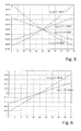
- Fig. 5 shows diagrams of progressions of the first phase ⁇ 1 and the second phase position ⁇ 2 as a function of the position p of the transmitting element for various preferred embodiments.
- the phases of the phase positions ⁇ 1 and ⁇ 2 are plotted for two different devices 10, which are identical in the parameters set out above, but which differ in the capacitors 17 in the respective end connections 19 a and 19 b.
- the different capacitances which distinguish the two configurations of the device 10, thereby cause a different slope of the change of the phase positions ⁇ 1 and ⁇ 2 .
- the somewhat larger capacitance of 150 nF of the capacitors 17 results in a smaller slope of the change of the phase positions ⁇ 1 and ⁇ 2 with changing position p of the transmitting element 20 than the somewhat small capacitance of 68 nF of the capacitors 17.
- the device has greater sensitivity than the otherwise similar device, which, unlike the first configuration, each has a capacitor 17 having a capacitance of 150 nF in the first and the second end connection 19a and 19b.
- the dependence of the gradient of the course of the phase positions ⁇ 1 and ⁇ 2 can in particular be understood by the term ( ⁇ RC ) 2 in the denominator of the formulas for the first phase position ⁇ 1 and the second phase position ⁇ 2 increasing capacity C increases quadratically, while the remaining terms in the denominator, which depend on p, do not grow with increasing capacity C.
- the ( ⁇ RC ) 2 dominates the denominator or the phase position ⁇ 1 or ⁇ 2 and / or the further terms which depend on p become increasingly negligible.
- phase positions ⁇ 1 and ⁇ 2 can be expressed by the following formulas: ⁇ 1 p ⁇ arctan 1 ⁇ RC p - p Max 2 ⁇ 2 p ⁇ - arctan 1 ⁇ RC p - p Max 2
- FIG. 12 shows plots of phase shift characteristics between the first phase ⁇ 1 and the second phase ⁇ 2 as a function of the position p of the transmission element for the two different configurations of the device 10 already described with reference to FIG Fig. 5 have been described.
- Fig. 6 It can be seen in this case also includes the graph of the phase shift ⁇ ⁇ (p) has a different slope for different capacitances of the capacitors 17 in the final compounds 19a and 19b.
- the deviations from a linear course are smaller than in the graphs of the individual phase positions ⁇ 1 and ⁇ 2 . This may be due, for example, to the fact that the contributions which lead to the deviation at least partially fall out during the subtraction or during the phase shift ⁇ ( p ).
- Figs. 7A to 7C show schematic representations of the time course of different voltage variables in a preferred embodiment of a device according to the invention for determining the position during operation.
- Fig. 7A shows the time course of the electrical voltage U ind , which is induced by the transmitting element 20 in the receiving module 10.
- Figs. 7B and 7C show the voltage U 1 and U 2 dropping at the first end connection 19 a and at the second end connection 19 B, respectively.
- the illustrated time profiles of the respective voltages are limited to a measurement cycle MZ, ie the course of the voltage during the power cycle LZ is not shown, since this is typically not taken into account for the position determination.
- a vertical auxiliary line VH which extends over all three figures Figs. 7A to 7C extends, marks an arbitrary point in time at which the respective phase angle ⁇ ind the induced voltage U ind , the first phase position ⁇ 1 of the first voltage U 1 and the second phase position ⁇ 2 of the second voltage U 2 are considered. It can be seen that the three voltages U ind , U 1 and U 2 do not oscillate in phase, but that the first phase ⁇ 1 of the voltage U1 and the second phase ⁇ 2 of the voltage U 2 both with each other and from the phase position of the induced Voltage U ind are different.
- the differences in the phase positions are due to the reactances in the end connections 19a and 19b, which cause a phase shift of the voltage signal falling in the end connections 19a and 19b relative to the induced voltage U ind .
- the differences in the phase positions are dependent on p, ie on the number of electrically conductive cross connections 16, which are located between the respective end connection 19a or 19b and the position of the transmitting element 20 along the longitudinal extension x of the receiving module 12.
- phase position ⁇ 1 and / or the phase position ⁇ 2 relative to one another and / or relative to the phase position of the induced voltage U ind as the reference phase and / or the phase shift or phase difference between ⁇ 1 and ⁇ 2 are used, in accordance with the invention, the position p of the transmission module along the longitudinal extension x of the reception module to investigate.
- the invention has been described in some embodiments, especially on the basis of the implementation with resistance values in the interconnections and reactance values in the end connections, it can also be used in an analogous manner with the reversed roles of active and Reactance values are implemented and used.
- the implementations of the components and / or numerical values of the first and / or second electrical reactance values in the respective end connection of the first implementation are also transferable to the predetermined electrical reactance values in the plurality of interconnections in the second implementation.
- the explanations concerning the components and / or numerical values of the predetermined electrical resistance values in the cross connections of the first implementation are preferably also applicable to the first and / or second electrical resistance value in the respective end connection of the second implementation.
Priority Applications (1)
| Application Number | Priority Date | Filing Date | Title |
|---|---|---|---|
| EP15002662.3A EP3141869A1 (fr) | 2015-09-11 | 2015-09-11 | Detection de position par phases a l'aide de reactances finales |
Applications Claiming Priority (1)
| Application Number | Priority Date | Filing Date | Title |
|---|---|---|---|
| EP15002662.3A EP3141869A1 (fr) | 2015-09-11 | 2015-09-11 | Detection de position par phases a l'aide de reactances finales |
Publications (1)
| Publication Number | Publication Date |
|---|---|
| EP3141869A1 true EP3141869A1 (fr) | 2017-03-15 |
Family
ID=54145522
Family Applications (1)
| Application Number | Title | Priority Date | Filing Date |
|---|---|---|---|
| EP15002662.3A Withdrawn EP3141869A1 (fr) | 2015-09-11 | 2015-09-11 | Detection de position par phases a l'aide de reactances finales |
Country Status (1)
| Country | Link |
|---|---|
| EP (1) | EP3141869A1 (fr) |
Citations (2)
| Publication number | Priority date | Publication date | Assignee | Title |
|---|---|---|---|---|
| US4007454A (en) | 1975-09-12 | 1977-02-08 | Charles J. Cain | Apparatus for remotely determining the angular orientation, speed, and/or direction of rotation of objects |
| WO2007107353A1 (fr) * | 2006-03-21 | 2007-09-27 | Hochschule Mannheim Hochschule Für Technik Und Gestaltung | Capteur de mesure de course par le biais du déphasage du champ magnétique dans le cas d'un ligne à retard RC |
-
2015
- 2015-09-11 EP EP15002662.3A patent/EP3141869A1/fr not_active Withdrawn
Patent Citations (3)
| Publication number | Priority date | Publication date | Assignee | Title |
|---|---|---|---|---|
| US4007454A (en) | 1975-09-12 | 1977-02-08 | Charles J. Cain | Apparatus for remotely determining the angular orientation, speed, and/or direction of rotation of objects |
| WO2007107353A1 (fr) * | 2006-03-21 | 2007-09-27 | Hochschule Mannheim Hochschule Für Technik Und Gestaltung | Capteur de mesure de course par le biais du déphasage du champ magnétique dans le cas d'un ligne à retard RC |
| DE102006012952A1 (de) | 2006-03-21 | 2008-01-03 | Fachhochschule Mannheim Hochschule für Technik und Gestaltung | Vorrichtung und Verfahren zur Positionsbestimmung |
Similar Documents
| Publication | Publication Date | Title |
|---|---|---|
| EP2895889B1 (fr) | Système de détection de corps étrangers en métal pour des systèmes de transmission d'énergie inductive | |
| DE19631438C2 (de) | Wirbelstromsensor | |
| EP3335011B1 (fr) | Dipositif pour mesure d'une variable | |
| EP3124314B1 (fr) | Detection de corps etrangers, en particulier pour systemes de charge inductifs | |
| DE102010007620B9 (de) | Näherungssensor | |
| DE3840532C2 (fr) | ||
| EP2389564A1 (fr) | Procédé pour générer un signal de mesure électrique par induction, et dispositif de détection correspondant | |
| WO2016149723A1 (fr) | Serrure ou ferrure de fenêtre ou de porte | |
| EP3293499B1 (fr) | Procédé de fonctionnement d'un débitmètre magnétique inductif et débitmètre magnétique inductif | |
| EP2567262A2 (fr) | Détection d'un objet métallique ou magnétique | |
| EP0447653B1 (fr) | Capteur inductif de position | |
| DE102004053551A1 (de) | Vorrichtung zum Erfassen eines beweglichen oder bewegbaren elektrisch und/oder magnetisch leitenden Teiles | |
| EP3118591A1 (fr) | Appareil de mesure de niveau de remplissage | |
| EP3141869A1 (fr) | Detection de position par phases a l'aide de reactances finales | |
| EP3357742A1 (fr) | Dispositif de détection d'objets en particulier pour systèmes de charge | |
| EP3824323B1 (fr) | Détecteur servant à détecter du matériau électriquement conducteur | |
| EP3327431B1 (fr) | Appareil de mesure de conductivité inductif et procédé de fonctionnement d'un appareil de mesure de conductivité inductif | |
| EP3557188A1 (fr) | Bielle magnétisée destinée à la mesure de cours | |
| EP3975211B1 (fr) | Unification de résolveur et de d'alimentation inductive de rotor dans un cercle magnétique | |
| EP0805423A2 (fr) | Dispositif pour déterminer la validité de pièces de monnaie, jetons ou autres objets plats métalliques | |
| EP3015826B1 (fr) | Dispositif de capteur, outil de commande et son procédé d'utilisation | |
| WO2020125994A1 (fr) | Procédé et dispositif de détection de corps étrangers électriquement conducteurs lors de la transmission d'énergie inductive | |
| EP2184623A2 (fr) | Dispositif de capteur destiné à détecter un objet et son mouvement dans une zone de mesure du dispositif de capteur | |
| DE102013100841A1 (de) | Wegaufnehmer mit einem Sensorelement und einer Tauchspule |
Legal Events
| Date | Code | Title | Description |
|---|---|---|---|
| PUAI | Public reference made under article 153(3) epc to a published international application that has entered the european phase |
Free format text: ORIGINAL CODE: 0009012 |
|
| AK | Designated contracting states |
Kind code of ref document: A1 Designated state(s): AL AT BE BG CH CY CZ DE DK EE ES FI FR GB GR HR HU IE IS IT LI LT LU LV MC MK MT NL NO PL PT RO RS SE SI SK SM TR |
|
| AX | Request for extension of the european patent |
Extension state: BA ME |
|
| STAA | Information on the status of an ep patent application or granted ep patent |
Free format text: STATUS: THE APPLICATION IS DEEMED TO BE WITHDRAWN |
|
| 18D | Application deemed to be withdrawn |
Effective date: 20170916 |