EP3138366B1 - Schaltreglersteuerkreis - Google Patents
Schaltreglersteuerkreis Download PDFInfo
- Publication number
- EP3138366B1 EP3138366B1 EP15712009.8A EP15712009A EP3138366B1 EP 3138366 B1 EP3138366 B1 EP 3138366B1 EP 15712009 A EP15712009 A EP 15712009A EP 3138366 B1 EP3138366 B1 EP 3138366B1
- Authority
- EP
- European Patent Office
- Prior art keywords
- signal
- current
- pwm
- switching regulator
- switch
- Prior art date
- Legal status (The legal status is an assumption and is not a legal conclusion. Google has not performed a legal analysis and makes no representation as to the accuracy of the status listed.)
- Active
Links
- 238000000034 method Methods 0.000 claims description 39
- 230000001105 regulatory effect Effects 0.000 claims description 25
- 239000003990 capacitor Substances 0.000 claims description 17
- 230000004044 response Effects 0.000 claims description 16
- 230000008859 change Effects 0.000 claims description 5
- 230000001276 controlling effect Effects 0.000 claims description 5
- 230000007423 decrease Effects 0.000 claims description 5
- 230000003111 delayed effect Effects 0.000 claims description 3
- 238000012546 transfer Methods 0.000 claims description 3
- 230000008878 coupling Effects 0.000 claims 1
- 238000010168 coupling process Methods 0.000 claims 1
- 238000005859 coupling reaction Methods 0.000 claims 1
- 230000000630 rising effect Effects 0.000 description 10
- 230000033228 biological regulation Effects 0.000 description 5
- 230000009286 beneficial effect Effects 0.000 description 4
- 238000013459 approach Methods 0.000 description 2
- 238000013461 design Methods 0.000 description 2
- 230000007704 transition Effects 0.000 description 2
- 230000008901 benefit Effects 0.000 description 1
- 230000001934 delay Effects 0.000 description 1
- 238000010586 diagram Methods 0.000 description 1
- 238000007599 discharging Methods 0.000 description 1
- 230000003828 downregulation Effects 0.000 description 1
- 238000012544 monitoring process Methods 0.000 description 1
- NJPPVKZQTLUDBO-UHFFFAOYSA-N novaluron Chemical compound C1=C(Cl)C(OC(F)(F)C(OC(F)(F)F)F)=CC=C1NC(=O)NC(=O)C1=C(F)C=CC=C1F NJPPVKZQTLUDBO-UHFFFAOYSA-N 0.000 description 1
- 230000003071 parasitic effect Effects 0.000 description 1
- 230000008569 process Effects 0.000 description 1
- 239000004065 semiconductor Substances 0.000 description 1
Images


Classifications
-
- H—ELECTRICITY
- H05—ELECTRIC TECHNIQUES NOT OTHERWISE PROVIDED FOR
- H05B—ELECTRIC HEATING; ELECTRIC LIGHT SOURCES NOT OTHERWISE PROVIDED FOR; CIRCUIT ARRANGEMENTS FOR ELECTRIC LIGHT SOURCES, IN GENERAL
- H05B45/00—Circuit arrangements for operating light-emitting diodes [LED]
- H05B45/10—Controlling the intensity of the light
-
- H—ELECTRICITY
- H02—GENERATION; CONVERSION OR DISTRIBUTION OF ELECTRIC POWER
- H02M—APPARATUS FOR CONVERSION BETWEEN AC AND AC, BETWEEN AC AND DC, OR BETWEEN DC AND DC, AND FOR USE WITH MAINS OR SIMILAR POWER SUPPLY SYSTEMS; CONVERSION OF DC OR AC INPUT POWER INTO SURGE OUTPUT POWER; CONTROL OR REGULATION THEREOF
- H02M3/00—Conversion of DC power input into DC power output
- H02M3/02—Conversion of DC power input into DC power output without intermediate conversion into AC
- H02M3/04—Conversion of DC power input into DC power output without intermediate conversion into AC by static converters
- H02M3/10—Conversion of DC power input into DC power output without intermediate conversion into AC by static converters using discharge tubes with control electrode or semiconductor devices with control electrode
- H02M3/145—Conversion of DC power input into DC power output without intermediate conversion into AC by static converters using discharge tubes with control electrode or semiconductor devices with control electrode using devices of a triode or transistor type requiring continuous application of a control signal
- H02M3/155—Conversion of DC power input into DC power output without intermediate conversion into AC by static converters using discharge tubes with control electrode or semiconductor devices with control electrode using devices of a triode or transistor type requiring continuous application of a control signal using semiconductor devices only
- H02M3/156—Conversion of DC power input into DC power output without intermediate conversion into AC by static converters using discharge tubes with control electrode or semiconductor devices with control electrode using devices of a triode or transistor type requiring continuous application of a control signal using semiconductor devices only with automatic control of output voltage or current, e.g. switching regulators
- H02M3/158—Conversion of DC power input into DC power output without intermediate conversion into AC by static converters using discharge tubes with control electrode or semiconductor devices with control electrode using devices of a triode or transistor type requiring continuous application of a control signal using semiconductor devices only with automatic control of output voltage or current, e.g. switching regulators including plural semiconductor devices as final control devices for a single load
-
- Y—GENERAL TAGGING OF NEW TECHNOLOGICAL DEVELOPMENTS; GENERAL TAGGING OF CROSS-SECTIONAL TECHNOLOGIES SPANNING OVER SEVERAL SECTIONS OF THE IPC; TECHNICAL SUBJECTS COVERED BY FORMER USPC CROSS-REFERENCE ART COLLECTIONS [XRACs] AND DIGESTS
- Y02—TECHNOLOGIES OR APPLICATIONS FOR MITIGATION OR ADAPTATION AGAINST CLIMATE CHANGE
- Y02B—CLIMATE CHANGE MITIGATION TECHNOLOGIES RELATED TO BUILDINGS, e.g. HOUSING, HOUSE APPLIANCES OR RELATED END-USER APPLICATIONS
- Y02B20/00—Energy efficient lighting technologies, e.g. halogen lamps or gas discharge lamps
- Y02B20/30—Semiconductor lamps, e.g. solid state lamps [SSL] light emitting diodes [LED] or organic LED [OLED]
Definitions
- This disclosure relates generally to switching regulators and, more particularly, to switching regulator control circuits.
- Regulators, or converters, including a switch, sometimes referred to as a power switch, for transferring energy from an input, such as an AC or DC voltage or current source, to a regulated output are well known.
- a switch sometimes referred to as a power switch
- the switch turns on and off to regulate the output.
- the switch operates in its active, or saturation region.
- Common switching regulator configurations include Buck, Boost, Buck-Boost, flyback, SEPIC, C ⁇ k, half bridge, and full bridge to name a few.
- various control methodologies for controlling conduction of the power switch can be applied to switching regulators, including Pulse Width Modulation (PWM) and Pulse Frequency Modulation (PFM), and for each of these control methodologies, various feedback and feed forward techniques are possible including voltage mode control and current mode control.
- PWM Pulse Width Modulation
- PFM Pulse Frequency Modulation
- Switching regulators are often used to provide a regulated current to drive an LED load as may include one or multiple LEDs coupled in series and/or parallel. Such switching regulators control the intensity or brightness of the LEDs by selectively dimming the LEDs.
- LED dimming sometimes referred to as analog dimming
- the intensity of the LEDs is adjusted by adjusting the regulated LED current.
- Analog dimming may utilize an error amplifier which is responsive to a reference signal and to a feedback signal proportional to the regulator output to generate an error signal.
- the error signal is then used to generate a switch control signal to control conduction of the switch and the resulting regulated current. For example, the error signal may be compared to a ramp signal to generate the switch control signal with a duty cycle suitable for regulating the LED current at a desired level.
- the intensity of the LEDs is adjusted by turning them off and on in response to a PWM signal at a variable duty cycle with a fixed DC current and frequency (typically 100Hz to 1KHz).
- the PWM signal may be externally provided or internally generated.
- analog dimming can be less complicated to implement than PWM dimming and PWM dimming pulses the LED current, which can cause visible flicker, audible noise, or EMI issues.
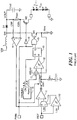
- Figure 1 illustrates a Boost regulator driving an LED load with current mode control that permits both PWM dimming and analog dimming.
- Analog dimming is achieved by adjusting the reference of the error amplifier (I1) according to the voltage on an external pin.
- the IREF pin is the external input that can be used to control the error amplifier reference when the voltage is below 1.0V.
- comparator 110 changes the state of analog multiplexer ("mux") I13, running the error amplifier off of the internal reference, which may be more accurate than the voltage supplied on the IREF pin.
- This feature is sometimes implemented by adding an additional positive input to the error amplifier (II) that overrides the internal reference when the external signal is less than the internal reference.
- the user controls the intensity of the LEDs by supplying a digital PWM signal into the PWM pin in Figure 1 .
- some LED regulators may include the generation of the PWM signal on chip, in which case the user supplies an analog signal that is translated into a PWM duty cycle.
- the SW node when the PWM signal is low the SW node is tri-stated with AND gate 15 to cause the LED current to be disabled.
- many LED regulators also tri-state the COMP node by introducing switch SW1. This technique allows the control loop to quickly recover when the regulator is re-enabled on the PWM input rising edge. Without switch SW1 the error amplifier (I1) would have to slew the
- US 2010/289424 A1 relates to methods and circuits for LED drivers, and in particular to methods for PWM dimming controls for LEDs of a display. Methods are described for PWM dimming control of LEDs, where respective currents for each LED channel are matched to one another and also where the brightness level of any channel of the LEDs is matched to within a certain brightness level of other channels of the LEDs, in addition to current sense and artificial ramp circuits for PWM dimming control.
- US 2012/286687 A1 discloses a semiconductor light source lighting circuit including a switching regulator that produces a drive current with a switching element, and a control circuit that controls turning on and off of the switching element so that the magnitude of the drive current approaches a target value.
- the control circuit includes an error comparator that compares the drive current and the target value, an up/down counter that performs a counting operation, in which the control digital value is incremented or decremented based on the result of the comparison, a D/A converter that converts the control digital value into an analog duty ratio setting signal, and a drive circuit that controls the turning on and off of the switching element based on the signal.
- the up/down counter stops the counting operation when the switching regulator is brought into the inactive state.
- the present invention provides a switching regulator control circuit as claimed in claim 1.
- the regulated output is a regulated current to drive an LED load
- the LED is dimmed in response to a PWM signal, but in conjunction with a controlled ramping the LED current in response to the reference signal.
- EMI and other issues caused by instantaneously turning on and off the switch are alleviated by slowly ramping the LED current up when turning on the LEDs and down when turning off the LEDs in a well controlled fashion.
- the described arrangement reduces control loop overshoot when the LEDs are turned back on after dimming.
- the described circuits and methods reduce EMI while allowing for good low duty cycle performance.
- the regulated output may be a current and the reference signal ramped down to control the rate of decrease of the regulated output.
- the reference signal may be ramped at a rate established in part by a capacitor and/or at a user programmable rate.
- the reference signal may be provided with a first rate of increase established by a first current source during a first, soft start time interval and with a second, faster rate of increase established by a second current source during a second time interval.
- the invention provides a method of dimming an LED according to claim 9.
- This aspect includes providing a PWM signal to a switch to turn the switch on in response to an associated one of a rising edge and a falling edge of the PWM signal and to turn the switch off in response to the other one of the rising edge and the falling edge of the PWM signal.
- the LED current is ramped down in response to the one of the rising edge or the falling edge or the PWM signal associated with turning off the switch.
- the LED current may be ramped down by delaying turning off the switch following a transition of the PWM signal. The delay may be established based on the reference signal crossing a predetermined threshold.
- the reference signal may be ramped at a rate established in part by a capacitor and/or at a user programmable rate.
- a soft start feature may be implemented.
- the ramping of the reference signal may be subject to a timeout feature.
- a second switch, coupled in series with the LED load, may be controlled by a linear regulator in response to the reference signal.
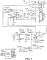
- a switching regulator including a switch M1 that conducts to transfer energy from an input source VIN to an output at which a regulated output is provided, further includes a circuit configured to generate a control signal to control conduction of the switch M1 and having a first input responsive to a reference signal (e.g., as provided at IREF), a second input responsive to a feedback signal proportional to the regulated output (e.g., as provided by 14), and an output at which the control signal is provided.
- the IREF reference signal is ramped to control a rate of change (i.e., increase and/or decrease) of the regulated output (I LED ) to implement a ramp control feature.
- the regulator control circuit further includes a logic circuit I5 coupled to the output of the circuit to gate the control signal in response to a PWM INT signal.
- the regulator control circuit includes a current source (114) and a current sink (115) coupled to the IREF pin along with an external cap (C IREF ) to slowly ramp the IREF voltage.
- the LED current I LED will slowly ramp with the IREF voltage at a rate established by a current source (114, 116) or current sink (115) and the value of the capacitor C IREF , as will be described.
- the use of external cap C IREF allows the user to program the ramp rate, typically on the order of 10u-100us.
- the regulator also includes a 10%, IREFLO comparator (I11), 110% high impedance driver (I12), IREF pull down (SW3), and digital controller I20 to form the ramp control feature.
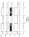
- the ramp control feature is only active after the rising and falling edges of the PWM input.
- the PWM input goes from low to high the IREF pin starts at 0V and ramps up past the internal reference (here of 1.0V) at a rate determined by the IREF capacitance and the source current of source 114 (T1 to T2).
- the LED current I LED tracks the IREF pin voltage, slowly ramping up with IREF voltage.
- the IREFHI signal also disables the source current 114 with the source signal and activates the 110% driver (I12) with the clamp signal. This prevents IREF from continuing to charge well past the 1.0V reference while ensuring that IREF does not drop below the 1.0V reference.
- the driver (112) may be implemented with an OTA connected as a buffer to a 1.1V reference that only has a source and sink capability on the order of 10uA.
- This high impendence drive allows the user to easily override the driver, and pull the reference IREF below 1.0V to set an analog dim reference. Note that when the IREF pin is pulled below the IREFHI comparator 110, the 110% driver 112 is disabled with switch SW2.
- the system may also be designed to detect the analog dim mode of operation and disable the source and sink currents (114 and 115) to provide better accuracy.
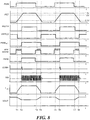
- the PWM INT signal causes the SW operation to resume, LED switch to close (M2), and COMP switch (SW1) to close on the rising edge of PWM INT .
- the LED current only jumps to the 10% level when the LED switch is closed (M2), due to the discharge characteristic, which will be explained in more detail later.
- the ramp control feature begins to slowly ramp up the IREF pin resulting in a slow ramp up of the LED current (I LED ), LED voltage (VOUT) and the COMP voltage.
- the clamp When the PWM input goes from high to low, the clamp is disabled and the IREF pin is discharged with the sink current (115) starting at the 1.1V reference, and the LED current I LED then begins to ramp down as it tracks the IREF voltage at the 1.0V handoff, as shown in Figure 4 .
- the LED switch (M2) would turnoff immediately with the PWM falling edge, but with the ramp control feature, the LED switch M2 must be closed while the LED current I LED is being ramped down. This delay is implemented by the digital controller (120) via the PWM INT signal. After the PWM input falling edge, the PWM INT signal remains high until the IREF pin voltage reaches the 10% threshold (i.e., until the IREFLO signal transitions at time T4).
- the PWM INT signal is a delayed version of the signal at the PWM input, where the delay corresponds to the time it takes the voltage at the IREF pin to fall to the 10% threshold (established by comparator I11) on the falling edge of the PWM signal and/or where the delay corresponds to the time it takes the voltage at the IREF pin to exceed the 10% threshold on the rising edge of the PWM signal.
- T4 the LED switch (M2) is opened, SW operation is halted, and the COMP node is tri-stated with switch SW1.
- the COMP node is tri-stated to save the control loop operating point while the output is not active so that when operation resumes, the control loop will resume regulation very quickly. In this case the operating point was at the 10% level so operation will also resume at the 10% level.
- ramp down regulation i.e., control of the rate of decrease of the LED current I LED via the IREF voltage
- This non-zero threshold is selected because when LED current is ramping down, the system is relying on the LED string to discharge the output capacitor (Cout). As the current gets lower, the ability of the LEDs to discharge the output capacitance is reduced, which may cause the LED current to remain higher than the reference set by the IREF pin.
- the regulator in Figure 3 does not have any current sink capability due to diode D1, and therefore the fastest rate the LEDs can be discharge at is set by Cout and the V-I characteristic of the LEDs (D LED ). Due to the exponential V-I characteristic of LEDs, the rate that Cout discharges at decreases with current. Therefore, the 10% turnoff threshold is selected so that LEDs still have enough sink capability to approximately track the IREF voltage.
- the 10% cutoff is also beneficial for the PWM input rising edge because the regulator cannot regulate LED current down to extremely low levels due to DCM (discontinuous conduction mode) operation and the SW node min duty cycle limit. For that reason, 10% is also selected as a point where the control loop can easily maintain the LED current. As shown in Figure 4 , it is desirable that the control is resumed at the same level (10%) that it was disabled at. This is because the LED voltage (VOUT) has been discharged to that level, and the COMP node is set to that level. Note that the COMP node has a step response on the PWM INT falling and rising edges due to the zero introduced by R1 in the compensation network. Since COMP is slewing, a voltage is developed across R1 that is eliminated when SW1 opens. When the controller is re-enabled the COMP node exhibits some overshoot to slew the inductor current up to the correct level.
- One light load control technique is pulse skipping which can be implemented by introducing an offset in the current sense signal, as shown in Figure 3 with 400mV node on 17. Therefore, when the COMP voltage drops below the 400mV reference, the SW node will stop switching and resume when the COMP voltage rises above the 400mV pedestal.
- This technique along with other light load control techniques, such as pulse frequency modulation, constant on time, etc. are well understood by those skilled in the art.
- the 10% IREFLO threshold results in a small 10% step in the LED current when the LED switch (M2) is open and closed.
- the small magnitude of this step should not cause significant EMI issues.
- the edge rate can be reduced with the addition of a small capacitor in parallel with the LEDs (C LED ).
- This capacitor (C LED ) should be at least one to several orders of magnitude smaller than the Cout capacitor.
- the control circuit is designed to provide the area under the curve when ramping up summed with the area when ramping down to be the same area as if the control feature were not present.
- the IREF pin source and sink currents (114 and 115) may be identical, and implemented with good relative accuracy.
- the IREF driver (112) reference is selected to be 10% above the reference handoff point (1.0V). This method relies on the IREF driver (112) to be accurate relative to the 1.0V internal reference.
- the LED current may not exactly track the IREF pin. This is especially true when a fast LED current slew rate is desired or a large output capacitor (Cout) or compensation capacitor (C1) is used.
- the current sink and source capability of the error amplifier can also impact the ability of the control loop to track the IREF voltage.
- the IREF pin slew rate should be adjusted until the desired LED current ramp rate is achieved.
- Figure 5 illustrates how the system operates with fast LED current slew rates, where the LED current does not exactly track the IREF pin (the expected LED current is shown with dashed lines). As illustrated, the faster ramp and/or slower control loop results in a larger step in the LED current at the PWM INT rising and falling edges.
- the error amplifier source and sink capability could be altered. Large signal control techniques could also be used to slew the COMP pin when the difference between feedback input and the IREF input becomes too large. Similar to this approach would be to simply ramp the COMP pin in an open loop fashion. These methods may be extended even further when using a digital control loop.
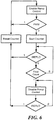
- a ramp control timeout feature or other similar function may be implemented.
- a timeout feature may be especially important when IREF is ramping down because the ramp control feature delays the tri-stating of the SW node (forcing off Ml) and the opening of the LED switch (M2) until IREF crosses the IREFLO threshold. This delay will result in the PWM input being ignored when the IREF input is driven with a DC signal for analog dimming.
- a timeout also allows the user to disable the ramp control feature during PWM dimming by driving the IREF pin above the 1.OV reference. This is beneficial if the ramp control feature is not desirable because floating the IREF pin may not fully eliminate the ramp control impact due to the parasitic capacitance on the IREF pin.
- FIG. 6 details the operation of an illustrative ramp control timeout feature.
- the ramp control timeout is only monitored on the PWM falling edge, and the timeout timer starts when the PWM input goes low.
- the IREF pin is initialized to a startup state. This is done in Figure 3 with SW3 and the IREFPD signal that comes from the digital controller 120, to pull down on the IREF pin.
- the ramp control architecture lends itself to including a soft start feature, such as the implementation shown in Figure 3 .
- the reference signal IREF is provided with a first rate of increase (i.e., ramps up at a first rate) established by a current source 116 to implement the soft start feature during a first, soft start time interval and is provided with a second, faster rate of increase established by a current source 114 to implement the ramp control feature during a second time interval.
- the respective current source control signals are provided by the digital controller, as shown.
- the ramp control feature is implemented with 10uA sink and source currents (114 and 115), whereas the soft start ramp is implemented with a 1uA current source (116). This results in a soft start ramp that is 10x slower the ramp control rate. Other ratios may be used.
- the IREF pull down (SW3) is released and the 1uA soft start current (116) will be used to charge the IREF pin with the ramp control current sources disabled (I14 and 115).
- the soft start feature will be disabled, and the ramp control driver and current sources will be reengaged as described above.
- Figure 3 implements the soft start feature by simply ramping the reference of the error amplifier I1. Due to the fact the LEDs will not conduct current until there is a few volts across them, the current sense voltage (CSP-CSN) will remain at zero until VOUT reaches a few volts. As a result, the error amplifier will drive the COMP pin as hard as possible because the 0V current sense voltage (CSP-CSN) is not tracking the soft start ramp. This may result in some overshoot when the LEDs finally do begin to conduct. Fortunately this overshoot will occur at very low LED currents, and at that point the LED current will begin to track the soft start ramp. Other soft start circuits and techniques are also possible. One example is to change the feedback signal of the error amplifier from the current sense amplifier 14 to a resistor divider across VOUT until the LEDs begin to conduct.
- the ramp control feature can also be implemented using other circuitry and/or techniques in addition to or in place of the presented circuitry and techniques.
- One additional technique is illustrated in Figure 7 , which turns the PMOS LED switch (M2) into a linear regulator with the addition of amplifier I21.
- the reference of the linear regulator (121 and M2) is the IREF signal.
- This linear regulator technique does not suffer the limitations of the LED string discharging the output capacitor (Cout) explained earlier because M2 can control the LED current independent of the voltage across Cout. Therefore in Figure 7 the IREFLO threshold has been changed to 5% (50mV) to take advantage of this higher performance technique. In addition, the reference for driver 112 has been changed to 105% (1.05V) to properly cancel out the delay. Note that it is still beneficial to have a non-zero IREFLO threshold to be tolerant of errors in the circuitry and relax the design requirements of the linear regulator.
- the switching regulator When adding an additional control loop to regulate the LED current, as done in Figure 7 , it is important that the multiple loops do not negatively interact with one another. In this case, the switching regulator must simply supply enough current to support the current need of linear regulator 121. As shown in Figure 7 and 8 , this requirement is met by tri-stating COMP pin with the IREFHI signal so that the switching regulator continues to run as if the LEDs were continuing to sink the full regulation current. As a result, when ramping down the LED current, the output voltage (VOUT) will rise up as the output capacitor is charged with the excess current, as illustrated in Figure 8 .
- the switching regulator disabled, by shifting the PWM INT signal as shown in Figure 8 , so that excess charge in the output capacitor (Cout) is depleted as the LED current is ramped up.
- the linear regulator will naturally drive the LED switch (M2) into the triode region because the switching regulator will take over regulation by supplying less current than demanded by the linear regulator.
- the proposed ramp control circuitry and techniques can be applied any linear or switching regulator topology including but not limited to Buck, Boost, Buck-Boost, SEPIC, C ⁇ k, half-bridge, full bridge, and linear regulators.
- the described circuitry and techniques are not limited to mixed signal systems but can be applied using digital, analog, or software methods, such as a digital to analog converter or charge pump to replace the current sources and external capacitor on the IREF pin.
- the rate of the IREF pin could be defined by other parameters such as input voltage, output voltage, light intensity, or any other fixed or variable parameter.
- the ramp up and down characteristic does not need to be linear; for example, it can have an exponential characteristic or even a discontinuity in the shape if desired.
- the described circuitry and techniques can be implemented with any control loop including current mode control (as discussed and illustrated), voltage mode control, constant on time control, constant off time control, or any other analog and/or digital control scheme.
- the proposed circuitry and techniques are not limited to application in regulators that regulate current, and can be applied to regulators that instead regulate voltage, power, or other parameter.
- a regulator of the type described herein may operate in different dimming modes in conjunction and/or in addition to the dimming described herein that utilizes the ramp control feature.
Landscapes
- Engineering & Computer Science (AREA)
- Power Engineering (AREA)
- Circuit Arrangement For Electric Light Sources In General (AREA)
- Dc-Dc Converters (AREA)
Claims (15)
- Schaltreglersteuerschaltung zum Steuern eines Schaltreglers, umfassend einen Schalter (M1), der leitet, um Energie von einer Eingangsquelle (VIN) an einen Ausgang zu übertragen, an dem einer LED-Last (DLED) ein geregelter Ausgangsstrom (ILED) bereitgestellt wird, die Schaltreglersteuerschaltung Folgendes umfassend:eine Schaltung, die zum Erzeugen eines Steuersignals zum Steuern des Leitens des Schalters (M1) konfiguriert ist, und einen ersten Eingang, der auf ein Referenzsignal (IREF) anspricht, einen zweiten Eingang zum Empfangen eines Rückkopplungssignals, das proportional zu dem geregelten Ausgangsstrom (ILED) ist, und einen Ausgang, an dem das Steuersignal bereitgestellt wird, aufweist;wobei die Schaltung eine Stromquelle umfasst; dadurch gekennzeichnet, dass die Schaltung ferner eine Stromsenke umfasst, wobei die Stromquelle und die Stromsenke mit dem ersten Eingang gekoppelt sind,wobei das Referenzsignal durch eines aus der Stromquelle oder der Stromsenke rampenförmig erhöht wird, um eine Änderungsrate des geregelten Ausgangsstroms zu steuern;eine digitale Steuerung (120) zum Empfangen eines externen digitalen Signals (PWM) und zum Erzeugen eines PWM-Signals (PWMINT) als eine verzögerte Version des externen digitalen Signals; undeine Logikschaltung (15), die gekoppelt ist, um das Steuersignal am Ausgang der Schaltung zu empfangen, undkonfiguriert ist, das Steuersignal mit dem Schalter in Reaktion auf das PWM-Signal (PWMINT) selektiv zu koppeln, um die LED-Last zu dimmen, wobei das Referenzsignal durch mindestens eines aus der Stromquelle oder der Stromsenke in Reaktion auf eine Flanke des externen digitalen Signals rampenförmig erhöht wird, und wobei die Verzögerung zwischen dem externen digitalen Signal (PWM) und dem PWM-Signal (PWMINT) der von dem Referenzsignal für das Überschreiten eines Schwellenspannungspegels nach dem Auftreten der Flanke des externen digitalen Signals benötigten Zeit entspricht.
- Schaltreglersteuerschaltung nach Anspruch 1, wobei das Referenzsignal rampenförmig abgesenkt wird, um die Abnahmerate des geregelten Ausgangsstroms zu steuern.
- Schaltreglersteuerschaltung nach Anspruch 1 oder 2, wobei das Referenzsignal mit einer Rate rampenförmig erhöht wird, die teilweise durch einen Kondensator (CIREF) gebildet wird.
- Schaltreglersteuerschaltung nach Anspruch 1 oder 2, wobei das Referenzsignal mit einer benutzerprogrammierbaren Rate rampenförmig erhöht wird.
- Schaltreglersteuerschaltung nach Anspruch 4, wobei das Referenzsignal entsprechend einer von dem Benutzer ausgewählten Kapazität rampenförmig erhöht wird.
- Schaltreglersteuerschaltung nach einem der vorhergehenden Ansprüche, wobei dem Referenzsignal eine erste Erhöhungsrate bereitgestellt wird, die durch eine erste Stromquelle (116) während eines ersten, weichen Startzeitintervalls gebildet wird, und eine zweite, schnellere Erhöhungsrate bereitgestellt wird, die durch eine zweite Stromquelle (114) während eines zweiten Zeitintervalls gebildet wird.
- Schaltreglersteuerschaltung nach einem der vorhergehenden Ansprüche, wobei die Schaltung so angeordnet ist, dass sie das rampenförmige Erhöhen des geregelten Ausgangsstroms in Reaktion auf einen Timeout-Zustand stoppt.
- Schaltreglersteuerschaltung nach Anspruch 7, wobei der Timeout-Zustand umfasst, dass das Referenzsignal unter einen vorbestimmten Spannungspegel fällt.
- Verfahren zum Dimmen einer LED (DLED) in einem Schaltregler, der ausgebildet ist, um einer LED-Last einen 15 geregelten Ausgangsstrom bereitzustellen, und umfassend einen Schalter (M1), der leitet, um Energie von einer Eingangsquelle (VIN) an einen Ausgang zu übertragen, an dem der geregelte Ausgangsstrom (ILED) bereitgestellt wird, und eine Stromquelle und eine Stromsenke, das Verfahren Folgendes umfassend:Erzeugen eines Steuersignals zum Steuern des Leitens des Schalters (M1) in Reaktion auf ein Referenzsignal und ein Rückkopplungssignal, das proportional zu dem geregelten Ausgangsstrom ist;dadurch gekennzeichnet, dass das Verfahren ferner das rampenförmige Erhöhen des Referenzsignals durch eines aus der Stromquelle oder der Stromsenke in Reaktion auf eine Flanke eines externen digitalen Signals (PWM) umfasst, um die Änderungsrate des geregelten Ausgangsstroms zu steuern;Erzeugen eines PWM-Signals (PWMINT) als eine verzögerte Version des externen digitalen Signals und selektives Koppeln des Steuersignals mit dem Schalter in Reaktion auf das PWM-Signal, um die LED-Last zu dimmen, wobei die Verzögerung zwischen dem externen digitalen Signal (PWM) und dem PWM-Signal (PWMINT) der von dem Referenzsignal für das Überschreiten eines Schwellenspannungspegels nach dem Auftreten der Flanke des externen digitalen Signals benötigten Zeit entspricht.
- Verfahren nach Anspruch 9, wobei das Steuern der Änderungsrate des geregelten Ausgangsstroms das Verzögern des Ausschaltens eines zweiten Schalters (M2) umfasst, der mit der LED während eines Zeitintervalls, das auf das Auftreten der Flanke des externen digitalen Signals folgt, in Reihe geschaltet ist.
- Verfahren nach Anspruch 10, ferner umfassend das Bereitstellen eines zweiten Steuersignals an den zweiten Schalter, um den zweiten Schalter als einen Linearregler zu betreiben.
- Verfahren nach einem der Ansprüche 9 bis 11, wobei der geregelte Ausgangsstrom mit einer benutzerprogrammierbaren Rate rampenförmig erhöht wird.
- Verfahren nach einem der Ansprüche 9 bis 12, wobei der geregelte Ausgangsstrom mit einer Rate rampenförmig erhöht wird, die entsprechend der Auswahl einer Kapazität wählbar ist.
- Verfahren nach einem der Ansprüche 9 bis 13, ferner umfassend das Stoppen des rampenförmigen Erhöhens des geregelten Ausgangsstroms in Reaktion auf einen Timeout-Zustand.
- Verfahren nach Anspruch 14, wobei der Timeout-Zustand umfasst, dass das Referenzsignal unter einen vorbestimmten Schwellenspannungspegel fällt.
Applications Claiming Priority (3)
| Application Number | Priority Date | Filing Date | Title |
|---|---|---|---|
| US201462002417P | 2014-05-23 | 2014-05-23 | |
| US14/620,656 US9774257B2 (en) | 2014-05-23 | 2015-02-12 | Control circuit for a switching regulator driving an LED load with controlled PWM dimming |
| PCT/US2015/020057 WO2015179006A1 (en) | 2014-05-23 | 2015-03-12 | Switching regulator control circuit |
Publications (2)
| Publication Number | Publication Date |
|---|---|
| EP3138366A1 EP3138366A1 (de) | 2017-03-08 |
| EP3138366B1 true EP3138366B1 (de) | 2020-08-05 |
Family
ID=52727461
Family Applications (1)
| Application Number | Title | Priority Date | Filing Date |
|---|---|---|---|
| EP15712009.8A Active EP3138366B1 (de) | 2014-05-23 | 2015-03-12 | Schaltreglersteuerkreis |
Country Status (5)
| Country | Link |
|---|---|
| US (1) | US9774257B2 (de) |
| EP (1) | EP3138366B1 (de) |
| JP (1) | JP6510637B2 (de) |
| KR (1) | KR102215586B1 (de) |
| WO (1) | WO2015179006A1 (de) |
Families Citing this family (20)
| Publication number | Priority date | Publication date | Assignee | Title |
|---|---|---|---|---|
| JP6571918B2 (ja) * | 2014-10-02 | 2019-09-04 | ローム株式会社 | 発光素子駆動回路、発光装置、車両 |
| US10263515B2 (en) * | 2016-04-14 | 2019-04-16 | Licon Technology Corporation | Quasi-analog digital pulse-width modulation control |
| KR102490322B1 (ko) * | 2016-09-23 | 2023-01-19 | 포세온 테크날러지 인코퍼레이티드 | 사전-충전 조명 제어 회로 |
| US10033270B2 (en) * | 2016-10-26 | 2018-07-24 | International Business Machines Corporation | Dynamic voltage regulation |
| CN109842281B (zh) * | 2017-11-24 | 2020-12-01 | 南京德朔实业有限公司 | 电动工具 |
| US10367500B2 (en) | 2017-12-08 | 2019-07-30 | Allegro Microsystems, Llc | Switching voltage regulator with variable minimum off-time |
| JP2019129109A (ja) * | 2018-01-26 | 2019-08-01 | セイコーエプソン株式会社 | 光源装置、投写型表示装置、及び、半導体装置 |
| KR102306073B1 (ko) * | 2018-07-18 | 2021-09-29 | 이피션트 파워 컨버젼 코퍼레이션 | 집적된 버스 부스트 회로를 갖는 전류 펄스 발생기 |
| CN109309993B (zh) * | 2018-11-16 | 2024-02-27 | 苏州中储普华电力科技有限公司 | 用于智能照明的回路调光电路 |
| CN109379822A (zh) * | 2018-12-05 | 2019-02-22 | 大峡谷照明系统(苏州)股份有限公司 | 双回路灯光控制系统及其在高层异形建筑室外照明的应用 |
| KR102121194B1 (ko) * | 2019-08-21 | 2020-06-26 | 주식회사 다원디엔에스 | 과열이 방지되는 IoT 조명 스위치 모듈 |
| CN111063313A (zh) * | 2019-12-04 | 2020-04-24 | Tcl华星光电技术有限公司 | 控制电路及其应用的显示面板 |
| US11432385B2 (en) * | 2020-08-07 | 2022-08-30 | Analog Devices, Inc. | Single comparator exponential-scale PWM dimming |
| US11218161B1 (en) | 2020-11-16 | 2022-01-04 | Allegro Microsystems, Llc | Tracking analog-to-digital converter with adaptive slew rate boosting |
| US11272591B1 (en) | 2020-12-02 | 2022-03-08 | Allegro Microsystems, Llc | Constant power light emitting diode (LED) driver |
| FR3117622B1 (fr) * | 2020-12-11 | 2024-05-03 | St Microelectronics Grenoble 2 | Courant d'appel d'au moins un régulateur de tension à faible chute |
| US11711012B2 (en) | 2021-05-28 | 2023-07-25 | Allegro Microsystems, Llc | Synchronous converter for use with reverse current protection diode |
| US11703898B2 (en) | 2021-07-09 | 2023-07-18 | Allegro Microsystems, Llc | Low dropout (LDO) voltage regulator |
| CN114584118B (zh) * | 2022-03-03 | 2025-09-23 | 武汉船用电力推进装置研究所(中国船舶重工集团公司第七一二研究所) | 一种全海深耐压电子开关 |
| US12456971B2 (en) | 2023-11-30 | 2025-10-28 | Allegro Microsystems, Llc | Method and apparatus for limiting minority carrier injection |
Family Cites Families (31)
| Publication number | Priority date | Publication date | Assignee | Title |
|---|---|---|---|---|
| US5264782A (en) * | 1992-08-10 | 1993-11-23 | International Business Machines Corporation | Dropout recovery circuit |
| TW200504662A (en) | 2003-07-17 | 2005-02-01 | Analog Integrations Corp | Method of using current mirror to drive LED |
| TW200737066A (en) * | 2006-03-22 | 2007-10-01 | Beyond Innovation Tech Co Ltd | Driving circuit with protection module for back light module |
| US7868603B2 (en) | 2006-10-04 | 2011-01-11 | Microsemi Corporation | Method and apparatus to compensate for supply voltage variations in a PWM-based voltage regulator |
| US7675245B2 (en) | 2007-01-04 | 2010-03-09 | Allegro Microsystems, Inc. | Electronic circuit for driving a diode load |
| KR101370650B1 (ko) * | 2007-04-25 | 2014-03-10 | 페어차일드코리아반도체 주식회사 | 스위치 제어 장치, 스위치 제어 방법 및 이를 이용하는컨버터 및 그 구동방법 |
| WO2009064682A2 (en) | 2007-11-16 | 2009-05-22 | Allegro Microsystems, Inc. | Electronic circuits for driving series connected light emitting diode strings |
| US7999487B2 (en) | 2008-06-10 | 2011-08-16 | Allegro Microsystems, Inc. | Electronic circuit for driving a diode load with a predetermined average current |
| US8390262B2 (en) | 2008-11-17 | 2013-03-05 | Lepower Semiconductor Inc. | Methods and circuits for LED drivers and for PWM dimming controls |
| JP5091101B2 (ja) * | 2008-12-19 | 2012-12-05 | 株式会社リコー | ソフトスタート回路及びそのソフトスタート回路を備えた電源回路 |
| US8455794B2 (en) * | 2009-06-03 | 2013-06-04 | Illinois Tool Works Inc. | Welding power supply with digital control of duty cycle |
| TWI404454B (zh) | 2009-10-14 | 2013-08-01 | Analog Integrations Corp | 具大操作電壓範圍之發光二極體驅動電路 |
| JP5470150B2 (ja) * | 2010-04-23 | 2014-04-16 | ローム株式会社 | スイッチング電源の制御回路、制御方法およびそれらを用いた発光装置および電子機器 |
| JP5601020B2 (ja) * | 2010-05-19 | 2014-10-08 | ソニー株式会社 | 発光素子駆動装置および表示装置 |
| TWI441008B (zh) | 2010-09-15 | 2014-06-11 | Analog Integrations Corp | 穩定被動元件之功耗的方法 |
| US8901835B2 (en) | 2010-09-15 | 2014-12-02 | Analog Integrations Corporation | LED lighting systems, LED controllers and LED control methods for a string of LEDS |
| TWI434617B (zh) | 2011-01-28 | 2014-04-11 | Analog Integrations Corp | 可提高電能轉換效率的驅動電路與其驅動方法 |
| TWI430699B (zh) | 2011-01-28 | 2014-03-11 | Analog Integrations Corp | 可提高電能轉換效率的驅動電路及其驅動方法 |
| US8482225B2 (en) | 2011-04-28 | 2013-07-09 | Allegro Microsystems, Llc | Electronic circuits and methods for driving a diode load |
| JP5714976B2 (ja) | 2011-05-12 | 2015-05-07 | 株式会社小糸製作所 | 半導体光源点灯回路 |
| US9155156B2 (en) | 2011-07-06 | 2015-10-06 | Allegro Microsystems, Llc | Electronic circuits and techniques for improving a short duty cycle behavior of a DC-DC converter driving a load |
| US9265104B2 (en) | 2011-07-06 | 2016-02-16 | Allegro Microsystems, Llc | Electronic circuits and techniques for maintaining a consistent power delivered to a load |
| JP5947034B2 (ja) * | 2011-12-20 | 2016-07-06 | ローム株式会社 | Dc/dcコンバータおよび電流ドライバの制御回路ならびにそれらを用いた発光装置および電子機器 |
| US8610371B2 (en) | 2011-12-22 | 2013-12-17 | Allegro Microsystems, Llc | Circuitry to drive parallel loads sequentially |
| US20140084884A1 (en) * | 2012-07-06 | 2014-03-27 | Jong J. Lee | Lc switching regulators |
| US10368410B2 (en) | 2012-10-19 | 2019-07-30 | Linear Technology Corporation | PWM control for LEDs with reduced flicker when using spread spectrum switching frequencies |
| US8742682B1 (en) | 2012-11-28 | 2014-06-03 | Analog Integrations Corporation | AC driven lighting systems capable of avoiding dark zone |
| US8779805B1 (en) | 2012-12-26 | 2014-07-15 | Allegro Microsystems, Llc | Output driver having improved switching delay and associated methods |
| US9285812B2 (en) * | 2013-02-01 | 2016-03-15 | Allegro Microsystems, Llc | Soft start circuits and techniques |
| US9287772B2 (en) * | 2013-03-06 | 2016-03-15 | Vidatronic, Inc. | Voltage regulators with improved startup, shutdown, and transient behavior |
| US8937433B1 (en) | 2013-09-10 | 2015-01-20 | Analog Integrations Corporation | LED lighting systems, LED controllers and LED control methods for a string of LEDs |
-
2015
- 2015-02-12 US US14/620,656 patent/US9774257B2/en active Active
- 2015-03-12 JP JP2017514258A patent/JP6510637B2/ja active Active
- 2015-03-12 KR KR1020167033556A patent/KR102215586B1/ko active Active
- 2015-03-12 WO PCT/US2015/020057 patent/WO2015179006A1/en not_active Ceased
- 2015-03-12 EP EP15712009.8A patent/EP3138366B1/de active Active
Non-Patent Citations (1)
| Title |
|---|
| None * |
Also Published As
| Publication number | Publication date |
|---|---|
| WO2015179006A1 (en) | 2015-11-26 |
| JP2017521995A (ja) | 2017-08-03 |
| KR102215586B1 (ko) | 2021-02-15 |
| EP3138366A1 (de) | 2017-03-08 |
| US9774257B2 (en) | 2017-09-26 |
| KR20170009887A (ko) | 2017-01-25 |
| JP6510637B2 (ja) | 2019-05-08 |
| US20150340950A1 (en) | 2015-11-26 |
Similar Documents
| Publication | Publication Date | Title |
|---|---|---|
| EP3138366B1 (de) | Schaltreglersteuerkreis | |
| KR101679629B1 (ko) | 발광 다이오드 부하를 구동하는 전자 회로 및 방법 | |
| KR101314393B1 (ko) | 불연속 전도 모드 동안 스위치 모드 레귤레이터의 조정 정확성을 개선하기 위한 시스템 및 방법 | |
| US7872456B2 (en) | Discontinuous conduction mode pulse-width modulation | |
| US9143033B2 (en) | Hysteretic power converter with calibration circuit | |
| US7595624B2 (en) | Slope compensation for switching regulator | |
| EP3146799B1 (de) | Verfahren und system zur verbesserung der led-lebensdauer und der farbqualität und dimmungsvorrichtung | |
| US7733030B2 (en) | Switching power converter with controlled startup mechanism | |
| US20100320935A1 (en) | Current-regulated power supply with soft-start protection | |
| US20120223693A1 (en) | Methods and apparatus for dc-dc conversion using digitally controlled adaptive pulse frequency modulation | |
| US8829872B1 (en) | Systems and methods for dropping and/or adding phases in multiphase regulators | |
| CN102083257A (zh) | 用于在led驱动电路的非零负载状态期间提供过冲保护和灯开关模式的积分器 | |
| KR20160128385A (ko) | 공통 스위치 제어 신호를 이용하는 led 드라이버에 대한 부스트 덴 플로팅 벅 모드 컨버터 | |
| US20160302270A1 (en) | Power optimization for linear regulator | |
| US9660473B2 (en) | Controllers for DC/DC converter | |
| US9148918B2 (en) | Feedforward circuit for fast analog dimming in LED drivers | |
| TWI838215B (zh) | 控制器和用於開關調節器的控制器中的方法 | |
| US10193448B1 (en) | Method of forming a power supply control circuit and structure therefor | |
| KR20210082073A (ko) | 벅-부스트 변환기 회로 | |
| TW201510692A (zh) | 可以調整流經一元件之一直流電流的電子裝置與控制方法 | |
| Sepahvand et al. | Current control and PWM dimming in an automotive LED driver based on a Ćuk converter | |
| US20200228009A1 (en) | Power converter with multi-mode timing control |
Legal Events
| Date | Code | Title | Description |
|---|---|---|---|
| STAA | Information on the status of an ep patent application or granted ep patent |
Free format text: STATUS: THE INTERNATIONAL PUBLICATION HAS BEEN MADE |
|
| PUAI | Public reference made under article 153(3) epc to a published international application that has entered the european phase |
Free format text: ORIGINAL CODE: 0009012 |
|
| STAA | Information on the status of an ep patent application or granted ep patent |
Free format text: STATUS: REQUEST FOR EXAMINATION WAS MADE |
|
| 17P | Request for examination filed |
Effective date: 20161128 |
|
| AK | Designated contracting states |
Kind code of ref document: A1 Designated state(s): AL AT BE BG CH CY CZ DE DK EE ES FI FR GB GR HR HU IE IS IT LI LT LU LV MC MK MT NL NO PL PT RO RS SE SI SK SM TR |
|
| AX | Request for extension of the european patent |
Extension state: BA ME |
|
| DAV | Request for validation of the european patent (deleted) | ||
| DAX | Request for extension of the european patent (deleted) | ||
| STAA | Information on the status of an ep patent application or granted ep patent |
Free format text: STATUS: EXAMINATION IS IN PROGRESS |
|
| 17Q | First examination report despatched |
Effective date: 20180202 |
|
| RAP1 | Party data changed (applicant data changed or rights of an application transferred) |
Owner name: ALLEGRO MICROSYSTEMS, LLC |
|
| GRAP | Despatch of communication of intention to grant a patent |
Free format text: ORIGINAL CODE: EPIDOSNIGR1 |
|
| STAA | Information on the status of an ep patent application or granted ep patent |
Free format text: STATUS: GRANT OF PATENT IS INTENDED |
|
| INTG | Intention to grant announced |
Effective date: 20200203 |
|
| GRAS | Grant fee paid |
Free format text: ORIGINAL CODE: EPIDOSNIGR3 |
|
| GRAA | (expected) grant |
Free format text: ORIGINAL CODE: 0009210 |
|
| STAA | Information on the status of an ep patent application or granted ep patent |
Free format text: STATUS: THE PATENT HAS BEEN GRANTED |
|
| AK | Designated contracting states |
Kind code of ref document: B1 Designated state(s): AL AT BE BG CH CY CZ DE DK EE ES FI FR GB GR HR HU IE IS IT LI LT LU LV MC MK MT NL NO PL PT RO RS SE SI SK SM TR |
|
| REG | Reference to a national code |
Ref country code: GB Ref legal event code: FG4D |
|
| REG | Reference to a national code |
Ref country code: CH Ref legal event code: EP |
|
| REG | Reference to a national code |
Ref country code: AT Ref legal event code: REF Ref document number: 1300557 Country of ref document: AT Kind code of ref document: T Effective date: 20200815 |
|
| REG | Reference to a national code |
Ref country code: DE Ref legal event code: R096 Ref document number: 602015056870 Country of ref document: DE |
|
| REG | Reference to a national code |
Ref country code: IE Ref legal event code: FG4D |
|
| REG | Reference to a national code |
Ref country code: LT Ref legal event code: MG4D |
|
| REG | Reference to a national code |
Ref country code: NL Ref legal event code: MP Effective date: 20200805 |
|
| REG | Reference to a national code |
Ref country code: AT Ref legal event code: MK05 Ref document number: 1300557 Country of ref document: AT Kind code of ref document: T Effective date: 20200805 |
|
| PG25 | Lapsed in a contracting state [announced via postgrant information from national office to epo] |
Ref country code: SE Free format text: LAPSE BECAUSE OF FAILURE TO SUBMIT A TRANSLATION OF THE DESCRIPTION OR TO PAY THE FEE WITHIN THE PRESCRIBED TIME-LIMIT Effective date: 20200805 Ref country code: BG Free format text: LAPSE BECAUSE OF FAILURE TO SUBMIT A TRANSLATION OF THE DESCRIPTION OR TO PAY THE FEE WITHIN THE PRESCRIBED TIME-LIMIT Effective date: 20201105 Ref country code: LT Free format text: LAPSE BECAUSE OF FAILURE TO SUBMIT A TRANSLATION OF THE DESCRIPTION OR TO PAY THE FEE WITHIN THE PRESCRIBED TIME-LIMIT Effective date: 20200805 Ref country code: GR Free format text: LAPSE BECAUSE OF FAILURE TO SUBMIT A TRANSLATION OF THE DESCRIPTION OR TO PAY THE FEE WITHIN THE PRESCRIBED TIME-LIMIT Effective date: 20201106 Ref country code: NO Free format text: LAPSE BECAUSE OF FAILURE TO SUBMIT A TRANSLATION OF THE DESCRIPTION OR TO PAY THE FEE WITHIN THE PRESCRIBED TIME-LIMIT Effective date: 20201105 Ref country code: AT Free format text: LAPSE BECAUSE OF FAILURE TO SUBMIT A TRANSLATION OF THE DESCRIPTION OR TO PAY THE FEE WITHIN THE PRESCRIBED TIME-LIMIT Effective date: 20200805 Ref country code: FI Free format text: LAPSE BECAUSE OF FAILURE TO SUBMIT A TRANSLATION OF THE DESCRIPTION OR TO PAY THE FEE WITHIN THE PRESCRIBED TIME-LIMIT Effective date: 20200805 Ref country code: ES Free format text: LAPSE BECAUSE OF FAILURE TO SUBMIT A TRANSLATION OF THE DESCRIPTION OR TO PAY THE FEE WITHIN THE PRESCRIBED TIME-LIMIT Effective date: 20200805 Ref country code: PT Free format text: LAPSE BECAUSE OF FAILURE TO SUBMIT A TRANSLATION OF THE DESCRIPTION OR TO PAY THE FEE WITHIN THE PRESCRIBED TIME-LIMIT Effective date: 20201207 Ref country code: HR Free format text: LAPSE BECAUSE OF FAILURE TO SUBMIT A TRANSLATION OF THE DESCRIPTION OR TO PAY THE FEE WITHIN THE PRESCRIBED TIME-LIMIT Effective date: 20200805 |
|
| PG25 | Lapsed in a contracting state [announced via postgrant information from national office to epo] |
Ref country code: NL Free format text: LAPSE BECAUSE OF FAILURE TO SUBMIT A TRANSLATION OF THE DESCRIPTION OR TO PAY THE FEE WITHIN THE PRESCRIBED TIME-LIMIT Effective date: 20200805 Ref country code: RS Free format text: LAPSE BECAUSE OF FAILURE TO SUBMIT A TRANSLATION OF THE DESCRIPTION OR TO PAY THE FEE WITHIN THE PRESCRIBED TIME-LIMIT Effective date: 20200805 Ref country code: PL Free format text: LAPSE BECAUSE OF FAILURE TO SUBMIT A TRANSLATION OF THE DESCRIPTION OR TO PAY THE FEE WITHIN THE PRESCRIBED TIME-LIMIT Effective date: 20200805 Ref country code: LV Free format text: LAPSE BECAUSE OF FAILURE TO SUBMIT A TRANSLATION OF THE DESCRIPTION OR TO PAY THE FEE WITHIN THE PRESCRIBED TIME-LIMIT Effective date: 20200805 Ref country code: IS Free format text: LAPSE BECAUSE OF FAILURE TO SUBMIT A TRANSLATION OF THE DESCRIPTION OR TO PAY THE FEE WITHIN THE PRESCRIBED TIME-LIMIT Effective date: 20201205 |
|
| PG25 | Lapsed in a contracting state [announced via postgrant information from national office to epo] |
Ref country code: DK Free format text: LAPSE BECAUSE OF FAILURE TO SUBMIT A TRANSLATION OF THE DESCRIPTION OR TO PAY THE FEE WITHIN THE PRESCRIBED TIME-LIMIT Effective date: 20200805 Ref country code: CZ Free format text: LAPSE BECAUSE OF FAILURE TO SUBMIT A TRANSLATION OF THE DESCRIPTION OR TO PAY THE FEE WITHIN THE PRESCRIBED TIME-LIMIT Effective date: 20200805 Ref country code: EE Free format text: LAPSE BECAUSE OF FAILURE TO SUBMIT A TRANSLATION OF THE DESCRIPTION OR TO PAY THE FEE WITHIN THE PRESCRIBED TIME-LIMIT Effective date: 20200805 Ref country code: RO Free format text: LAPSE BECAUSE OF FAILURE TO SUBMIT A TRANSLATION OF THE DESCRIPTION OR TO PAY THE FEE WITHIN THE PRESCRIBED TIME-LIMIT Effective date: 20200805 Ref country code: SM Free format text: LAPSE BECAUSE OF FAILURE TO SUBMIT A TRANSLATION OF THE DESCRIPTION OR TO PAY THE FEE WITHIN THE PRESCRIBED TIME-LIMIT Effective date: 20200805 |
|
| REG | Reference to a national code |
Ref country code: DE Ref legal event code: R097 Ref document number: 602015056870 Country of ref document: DE |
|
| PG25 | Lapsed in a contracting state [announced via postgrant information from national office to epo] |
Ref country code: AL Free format text: LAPSE BECAUSE OF FAILURE TO SUBMIT A TRANSLATION OF THE DESCRIPTION OR TO PAY THE FEE WITHIN THE PRESCRIBED TIME-LIMIT Effective date: 20200805 |
|
| PLBE | No opposition filed within time limit |
Free format text: ORIGINAL CODE: 0009261 |
|
| STAA | Information on the status of an ep patent application or granted ep patent |
Free format text: STATUS: NO OPPOSITION FILED WITHIN TIME LIMIT |
|
| PG25 | Lapsed in a contracting state [announced via postgrant information from national office to epo] |
Ref country code: SK Free format text: LAPSE BECAUSE OF FAILURE TO SUBMIT A TRANSLATION OF THE DESCRIPTION OR TO PAY THE FEE WITHIN THE PRESCRIBED TIME-LIMIT Effective date: 20200805 |
|
| 26N | No opposition filed |
Effective date: 20210507 |
|
| PG25 | Lapsed in a contracting state [announced via postgrant information from national office to epo] |
Ref country code: IT Free format text: LAPSE BECAUSE OF FAILURE TO SUBMIT A TRANSLATION OF THE DESCRIPTION OR TO PAY THE FEE WITHIN THE PRESCRIBED TIME-LIMIT Effective date: 20200805 |
|
| PG25 | Lapsed in a contracting state [announced via postgrant information from national office to epo] |
Ref country code: SI Free format text: LAPSE BECAUSE OF FAILURE TO SUBMIT A TRANSLATION OF THE DESCRIPTION OR TO PAY THE FEE WITHIN THE PRESCRIBED TIME-LIMIT Effective date: 20200805 |
|
| PG25 | Lapsed in a contracting state [announced via postgrant information from national office to epo] |
Ref country code: MC Free format text: LAPSE BECAUSE OF FAILURE TO SUBMIT A TRANSLATION OF THE DESCRIPTION OR TO PAY THE FEE WITHIN THE PRESCRIBED TIME-LIMIT Effective date: 20200805 |
|
| REG | Reference to a national code |
Ref country code: CH Ref legal event code: PL |
|
| GBPC | Gb: european patent ceased through non-payment of renewal fee |
Effective date: 20210312 |
|
| REG | Reference to a national code |
Ref country code: DE Ref legal event code: R079 Ref document number: 602015056870 Country of ref document: DE Free format text: PREVIOUS MAIN CLASS: H05B0033080000 Ipc: H05B0044000000 |
|
| REG | Reference to a national code |
Ref country code: BE Ref legal event code: MM Effective date: 20210331 |
|
| PG25 | Lapsed in a contracting state [announced via postgrant information from national office to epo] |
Ref country code: IE Free format text: LAPSE BECAUSE OF NON-PAYMENT OF DUE FEES Effective date: 20210312 Ref country code: FR Free format text: LAPSE BECAUSE OF NON-PAYMENT OF DUE FEES Effective date: 20210331 Ref country code: GB Free format text: LAPSE BECAUSE OF NON-PAYMENT OF DUE FEES Effective date: 20210312 Ref country code: LU Free format text: LAPSE BECAUSE OF NON-PAYMENT OF DUE FEES Effective date: 20210312 Ref country code: LI Free format text: LAPSE BECAUSE OF NON-PAYMENT OF DUE FEES Effective date: 20210331 Ref country code: CH Free format text: LAPSE BECAUSE OF NON-PAYMENT OF DUE FEES Effective date: 20210331 |
|
| PG25 | Lapsed in a contracting state [announced via postgrant information from national office to epo] |
Ref country code: BE Free format text: LAPSE BECAUSE OF NON-PAYMENT OF DUE FEES Effective date: 20210331 |
|
| PG25 | Lapsed in a contracting state [announced via postgrant information from national office to epo] |
Ref country code: HU Free format text: LAPSE BECAUSE OF FAILURE TO SUBMIT A TRANSLATION OF THE DESCRIPTION OR TO PAY THE FEE WITHIN THE PRESCRIBED TIME-LIMIT; INVALID AB INITIO Effective date: 20150312 |
|
| PG25 | Lapsed in a contracting state [announced via postgrant information from national office to epo] |
Ref country code: CY Free format text: LAPSE BECAUSE OF FAILURE TO SUBMIT A TRANSLATION OF THE DESCRIPTION OR TO PAY THE FEE WITHIN THE PRESCRIBED TIME-LIMIT Effective date: 20200805 |
|
| PG25 | Lapsed in a contracting state [announced via postgrant information from national office to epo] |
Ref country code: MK Free format text: LAPSE BECAUSE OF FAILURE TO SUBMIT A TRANSLATION OF THE DESCRIPTION OR TO PAY THE FEE WITHIN THE PRESCRIBED TIME-LIMIT Effective date: 20200805 |
|
| PG25 | Lapsed in a contracting state [announced via postgrant information from national office to epo] |
Ref country code: TR Free format text: LAPSE BECAUSE OF FAILURE TO SUBMIT A TRANSLATION OF THE DESCRIPTION OR TO PAY THE FEE WITHIN THE PRESCRIBED TIME-LIMIT Effective date: 20200805 |
|
| PG25 | Lapsed in a contracting state [announced via postgrant information from national office to epo] |
Ref country code: MT Free format text: LAPSE BECAUSE OF FAILURE TO SUBMIT A TRANSLATION OF THE DESCRIPTION OR TO PAY THE FEE WITHIN THE PRESCRIBED TIME-LIMIT Effective date: 20200805 |
|
| PGFP | Annual fee paid to national office [announced via postgrant information from national office to epo] |
Ref country code: DE Payment date: 20241231 Year of fee payment: 11 |