EP3136819A1 - Heater and ignition device - Google Patents
Heater and ignition device Download PDFInfo
- Publication number
- EP3136819A1 EP3136819A1 EP15782910.2A EP15782910A EP3136819A1 EP 3136819 A1 EP3136819 A1 EP 3136819A1 EP 15782910 A EP15782910 A EP 15782910A EP 3136819 A1 EP3136819 A1 EP 3136819A1
- Authority
- EP
- European Patent Office
- Prior art keywords
- conductive layer
- heat
- generating resistor
- ceramic
- heater
- Prior art date
- Legal status (The legal status is an assumption and is not a legal conclusion. Google has not performed a legal analysis and makes no representation as to the accuracy of the status listed.)
- Granted
Links
Images


Classifications
-
- H—ELECTRICITY
- H05—ELECTRIC TECHNIQUES NOT OTHERWISE PROVIDED FOR
- H05B—ELECTRIC HEATING; ELECTRIC LIGHT SOURCES NOT OTHERWISE PROVIDED FOR; CIRCUIT ARRANGEMENTS FOR ELECTRIC LIGHT SOURCES, IN GENERAL
- H05B3/00—Ohmic-resistance heating
- H05B3/02—Details
- H05B3/06—Heater elements structurally combined with coupling elements or holders
-
- H—ELECTRICITY
- H05—ELECTRIC TECHNIQUES NOT OTHERWISE PROVIDED FOR
- H05B—ELECTRIC HEATING; ELECTRIC LIGHT SOURCES NOT OTHERWISE PROVIDED FOR; CIRCUIT ARRANGEMENTS FOR ELECTRIC LIGHT SOURCES, IN GENERAL
- H05B3/00—Ohmic-resistance heating
- H05B3/02—Details
-
- F—MECHANICAL ENGINEERING; LIGHTING; HEATING; WEAPONS; BLASTING
- F23—COMBUSTION APPARATUS; COMBUSTION PROCESSES
- F23Q—IGNITION; EXTINGUISHING-DEVICES
- F23Q7/00—Incandescent ignition; Igniters using electrically-produced heat, e.g. lighters for cigarettes; Electrically-heated glowing plugs
- F23Q7/001—Glowing plugs for internal-combustion engines
-
- H—ELECTRICITY
- H05—ELECTRIC TECHNIQUES NOT OTHERWISE PROVIDED FOR
- H05B—ELECTRIC HEATING; ELECTRIC LIGHT SOURCES NOT OTHERWISE PROVIDED FOR; CIRCUIT ARRANGEMENTS FOR ELECTRIC LIGHT SOURCES, IN GENERAL
- H05B3/00—Ohmic-resistance heating
- H05B3/10—Heating elements characterised by the composition or nature of the materials or by the arrangement of the conductor
- H05B3/12—Heating elements characterised by the composition or nature of the materials or by the arrangement of the conductor characterised by the composition or nature of the conductive material
-
- H—ELECTRICITY
- H05—ELECTRIC TECHNIQUES NOT OTHERWISE PROVIDED FOR
- H05B—ELECTRIC HEATING; ELECTRIC LIGHT SOURCES NOT OTHERWISE PROVIDED FOR; CIRCUIT ARRANGEMENTS FOR ELECTRIC LIGHT SOURCES, IN GENERAL
- H05B3/00—Ohmic-resistance heating
- H05B3/10—Heating elements characterised by the composition or nature of the materials or by the arrangement of the conductor
- H05B3/12—Heating elements characterised by the composition or nature of the materials or by the arrangement of the conductor characterised by the composition or nature of the conductive material
- H05B3/14—Heating elements characterised by the composition or nature of the materials or by the arrangement of the conductor characterised by the composition or nature of the conductive material the material being non-metallic
-
- H—ELECTRICITY
- H05—ELECTRIC TECHNIQUES NOT OTHERWISE PROVIDED FOR
- H05B—ELECTRIC HEATING; ELECTRIC LIGHT SOURCES NOT OTHERWISE PROVIDED FOR; CIRCUIT ARRANGEMENTS FOR ELECTRIC LIGHT SOURCES, IN GENERAL
- H05B3/00—Ohmic-resistance heating
- H05B3/10—Heating elements characterised by the composition or nature of the materials or by the arrangement of the conductor
- H05B3/18—Heating elements characterised by the composition or nature of the materials or by the arrangement of the conductor the conductor being embedded in an insulating material
-
- H—ELECTRICITY
- H05—ELECTRIC TECHNIQUES NOT OTHERWISE PROVIDED FOR
- H05B—ELECTRIC HEATING; ELECTRIC LIGHT SOURCES NOT OTHERWISE PROVIDED FOR; CIRCUIT ARRANGEMENTS FOR ELECTRIC LIGHT SOURCES, IN GENERAL
- H05B3/00—Ohmic-resistance heating
- H05B3/40—Heating elements having the shape of rods or tubes
- H05B3/42—Heating elements having the shape of rods or tubes non-flexible
- H05B3/48—Heating elements having the shape of rods or tubes non-flexible heating conductor embedded in insulating material
-
- H—ELECTRICITY
- H05—ELECTRIC TECHNIQUES NOT OTHERWISE PROVIDED FOR
- H05B—ELECTRIC HEATING; ELECTRIC LIGHT SOURCES NOT OTHERWISE PROVIDED FOR; CIRCUIT ARRANGEMENTS FOR ELECTRIC LIGHT SOURCES, IN GENERAL
- H05B2203/00—Aspects relating to Ohmic resistive heating covered by group H05B3/00
- H05B2203/027—Heaters specially adapted for glow plug igniters
Definitions
- a heater includes a ceramic multilayer body including a plurality of ceramic layers that are stacked together; a heat-generating resistor having a belt shape, the heat-generating resistor being disposed between the ceramic layers and arranged, and including both ends that are at a side surface of the ceramic multilayer body; and conductive layers having a belt shape, disposed between the ceramic layers and stacked on both end portions of the heat-generating resistor in such a manner that one end of each conductive layer is at the side surface.
- a heater 10 will be described with reference to the drawings.
- the ceramic multilayer body 1 is made of an electrically insulative ceramic, such as an insulating ceramic, a nitride ceramic, or a carbide ceramic. More specifically, the ceramic multilayer body 1 is made of, for example, an alumina ceramic, a silicon nitride ceramic, an aluminum nitride ceramic, or a silicon carbide ceramic.
- the length of the ceramic multilayer body 1 is set to, for example, 20 to 100 mm.
- the cross-sectional shape of the ceramic multilayer body 1 is set to, for example, a rectangle having a thickness of 1 to 6 mm and a width of 2 to 40 mm.
- the heat-generating resistor 2 is a layer-shaped member that generates heat when a voltage is applied thereto.
- the heat-generating resistor 2 is disposed between the adjacent ceramic layers 11.
- a voltage is applied to the heat-generating resistor 2
- a current flows through the heat-generating resistor 2
- the heat-generating resistor 2 generates heat.
- the generated heat is transferred through the ceramic multilayer body 1, so that the temperature of the surface of the ceramic multilayer body 1 increases.
- the heat is transferred from the surface of the ceramic multilayer body 1 to an object to be heated, thereby providing the function of the heater 10.
- the object to be heated that receives the heat from the surface of the ceramic multilayer body 1 is, for example, diesel oil to be supplied to an automobile diesel engine.
- the heat-generating resistor 2 is arranged in such a manner that both ends thereof are at a side surface of the ceramic multilayer body 1 near the rear end of the ceramic multilayer body 1.
- the heat-generating resistor 2 has, for example, a bent shape in longitudinal cross section (cross section parallel to the length direction of the heat-generating resistor 2). More specifically, the heat-generating resistor 2 includes two linear portions that are arranged next to each other and a connecting portion that has substantially semicircular or substantially semielliptical inner and outer peripheries and that is bent so as to connect the two linear portions.
- the heat-generating resistor 2 is bent at a location near the front end of the ceramic multilayer body 1.
- the total length of the heat-generating resistor 2 is, for example, 35 to 100 mm.
- the heat-generating resistor 2 is designed so as to generate a large amount of heat in a region near the front end of the ceramic multilayer body 1. More specifically, the conductive layers 3 are stacked on both end portions of the heat-generating resistor 2 in a region near the rear end of the ceramic multilayer body 1. Accordingly, a current flows through both the heat-generating resistor 2 and the conductive layers 3 in the region near the rear end of the ceramic multilayer body 1. As a result, the amount of heat generated by the heat-generating resistor 2 is small in the region near the rear end of the ceramic multilayer body 1. In contrast, the current flows only through the heat-generating resistor 2 in the region near the front end of the ceramic multilayer body 1. As a result, the amount of heat generated by the heat-generating resistor 2 is large in the region near the front end of the ceramic multilayer body 1.
- the heat-generating resistor 2 is made of, for example, a material having a carbide, nitride, silicide, etc., of tungsten (W), molybdenum (Mo), titanium (Ti), etc., as the main component.
- the heat-generating resistor 2 is preferably made of a material having tungsten carbide as the main component. In this case, the coefficient of thermal expansion of the ceramic multilayer body 1 and that of the heat-generating resistor 2 can be made close to each other.
- the conductive layers 3 are members for adjusting the amount of heat generated by the heat-generating resistor 2 in the region near the rear end of the ceramic multilayer body 1, that is, in the region around the portions of the side surface of the ceramic multilayer body 1 to which the heat-generating resistor 2 extends.
- the conductive layers 3 are shown by the broken lines.
- the broken lines that show the conductive layers 3 and the solid lines that show the heat-generating resistor 2 are shifted from each other to improve visibility.
- the conductive layers 3 and the heat-generating resistor 2 have substantially the same width, and are stacked together so as to be aligned with each other in the width direction. As illustrated in Figs.
- the conductive layers 3 are stacked on both end portions of the heat-generating resistor 2 in the space between the ceramic layers 11, and are arranged such that one end of each conductive layer 3 is at the side surface of the ceramic multilayer body 1.
- Each conductive layer 3 includes a first conductive layer 31 that extends to the side surface of the ceramic multilayer body 1 and a second conductive layer 32 that is adjacent to the first conductive layer 31.
- the first conductive layer 31 and the second conductive layer 32 are each formed of a plurality of grains.
- the average grain diameter of the grains of the first conductive layer 31 is smaller than that of the grains of the second conductive layer 32. Since the first conductive layer 31, which is located closer to the outside, is formed of grains having a small average grain diameter, the density of the first conductive layer 31 can be increased. As a result, the voidage of the first conductive layer 31 is reduced, and the risk that the outside air will flow into each conductive layer 3 can be reduced.
- the second conductive layer 32 is formed of grains having a large average grain diameter, the number of grain boundaries of the grains of the second conductive layers 32 can be reduced. Therefore, the resistance of the second conductive layer 32 can be reduced. Accordingly, unnecessary heat generation by each conductive layer 3 can be suppressed.
- the first conductive layer 31 and the second conductive layer 32 preferably partially overlap.
- each conductive layer 3 can be formed so as to have a coefficient of thermal expansion that changes gradually in the length direction thereof. As a result, the possibility that cracks will be formed in the conductive layers 3 in a heat cycle can be reduced.
- the first conductive layer 31 is located between the second conductive layer 32 and the heat-generating resistor 2, and, in a region in which the first conductive layer 31 is located between the second conductive layer 32 and the heat-generating resistor 2, the first conductive layer 31 has a thickness that decreases toward the other end thereof.
- each conductive layer 3 can be formed so as to have a coefficient of thermal expansion that changes smoothly. As a result, the possibility that cracks will be formed in the conductive layers 3 in a heat cycle can be further reduced.
- each conductive layer 3 includes only the first conductive layer 31 and the second conductive layer 32.
- each conductive layer 3 is not limited to this, and may further include a portion other than the first conductive layer 31 and the second conductive layer 32.
- each conductive layer 3 may include, in addition to the first conductive layer 31 and the second conductive layer 32, a third conductive layer 33.
- the third conductive layer 33 is adjacent to the second conductive layer 32 at a side opposite to the side adjacent to the first conductive layer 31.
- the layer used as the third conductive layer 33 may be formed of grains having an average grain diameter smaller than that of the grains of the second conductive layer 32. In such a case, the number of crystal grain boundaries of the grains of the third conductive layer 33 can be increased. Accordingly, the resistance of the third conductive layer 33 can be set to a value higher than that of the second conductive layer 32. Therefore, the amount of heat generated by the heat-generating resistor 2 can be changed gradually. Accordingly, the surface of the heater 10 can be heated in such a manner that the temperature thereof changes gradually. As a result, the risk that a large local thermal stress will be generated in the ceramic multilayer body 1 can be reduced.
- the first to third conductive layers 31 to 33 are made of, for example, a highly heat-resistant metal material, such as molybdenum (Mo), tungsten (W), or rhenium (Re). MoSi 2 , WSi 2 , etc., are preferably mixed in the material to make the coefficient of thermal expansion close to that of the ceramic multilayer body 1.
- the length of a portion of the first conductive layer 31 that extends in the length direction of the heat-generating resistor 2 is set to about 2 to 10 mm.
- the thickness of the first conductive layer 31 is set to about 5 to 30 ⁇ m.
- the length of a portion of the second conductive layer 32 that extends in the length direction of the heat-generating resistor 2 is set to about 5 to 20 mm.
- the thickness of the second conductive layer 32 is set to about 25 to 75 ⁇ m.
- the length of the overlapping region is set to, for example, about 500 ⁇ m.
- the grain diameters of the first conductive layer 31 and the second conductive layer 32 can be adjusted as follows.
- the grain diameters of the first conductive layer 31 and the second conductive layer 32 can be adjusted by changing the particle diameter of W powder, which is the starting material.
- the average grain diameter of the W powder used to form the first conductive layer 31 may be set to 0.2 ⁇ m
- the average grain diameter of the W powder used to form the second conductive layer 32 may be set to 1.2 ⁇ m.
- the average grain diameter of the first conductive layer 31 can be set to 0.2 to 2 ⁇ m
- the average grain diameter of the second conductive layer 32 can be set to 1.2 to 12 ⁇ m.
- the average grain diameter of the first conductive layer 31 is preferably less than 1 ⁇ m. In such a case, entrance of the outside air into the first conductive layer 31 through the spaces between the grains can be suppressed, and therefore the risk that the outside air will flow into the first conductive layer 31 can be reduced.
- the voidage of the first conductive layer is preferably less than 20%. In such a case, entrance of the outside air into the first conductive layer 31 can be suppressed.
- the average grain diameter of each conductive layer 3 can be determined by, for example, the following method. That is, the heater 10 is cut along a plane that passes through the conductive layer 3 and that is perpendicular to the conductive layer 3 by using a diamond cutter. Then, the cut surface is ground by using diamond powder. After that, the first conductive layer 31 and the second conductive layer 32 are observed by using a scanning electron microscope or metallographic microscope. More specifically, five arbitrary straight lines are drawn on the image obtained by the scanning electron microscope or metallographic microscope. Then, the average of the lengths of portions of the five straight lines, each portion passing through ten grains, is determined. The average grain diameter is determined by dividing the average by ten, which is the number of grains. The average grain diameter may instead be calculated by using an image analyzing device (LUZEX-FS produced by Nireco Corporation). This image analyzing device can also be used to measure the voidage of the first conductive layer 31.
- an image analyzing device (LUZEX-FS produced by Nireco Corporation). This image
- the heater 10 is used in, for example, an ignition device 100 illustrated in Fig. 5 .
- the ignition device 100 includes the heater 10 and a channel 20 through which fuel gas is supplied to the heater 10.
- the channel 20 includes, for example, a gas valve 21 and a gas flow pipe 22 having ejection holes 23.
- the gas valve 21 has a function of controlling the flow rate of the fuel gas.
- the fuel gas supplied from the gas valve 21 is, for example, natural gas or propane gas.
- the gas flow pipe 22 ejects the fuel gas, which is supplied from the gas valve 21, toward the heater 10 through the ejection holes 23.
- the ejected fuel gas can be ignited by heating the fuel gas with the heater 10.
- the ignition device 100 which includes the heater 10 having improved long-term reliability, has increased fuel-gas ignition stability.
Landscapes
- Engineering & Computer Science (AREA)
- Chemical & Material Sciences (AREA)
- Combustion & Propulsion (AREA)
- Mechanical Engineering (AREA)
- General Engineering & Computer Science (AREA)
- Resistance Heating (AREA)
Abstract
Description
- The present invention relates to a heater and an ignition device.
- A heater (ceramic heater) in which a heat-generating body is disposed in a ceramic body is known as an example of a heater for use in a gas stove, an on-vehicle heating device, a kerosene fan heater, a glow plug of an automobile engine, or the like.
Patent Document 1 discloses an example of a ceramic heater. - Japanese Unexamined Patent Application Publication No.
2000-156275 - The ceramic heater described in
Patent Document 1 has a risk that cracks will be formed in the feeder lines when the ceramic heater is repeatedly used in a high-temperature environment. When, in particular, cracks are formed in portions of the feeder lines exposed at the surface of the ceramic structure, the outside air may flow into the feeder lines. Therefore, the resistance of the feeder lines may change due to a reaction between the feeder lines and the outside air, and abnormal local heat generation may occur. Thus, it is difficult to increase the long-term reliability when the ceramic heater is repeatedly used in a high-temperature environment. - A heater includes a ceramic multilayer body including a plurality of ceramic layers that are stacked together; a heat-generating resistor having a belt shape, the heat-generating resistor being disposed between the ceramic layers and arranged, and including both ends that are at a side surface of the ceramic multilayer body; and conductive layers having a belt shape, disposed between the ceramic layers and stacked on both end portions of the heat-generating resistor in such a manner that one end of each conductive layer is at the side surface. Each conductive layer includes a first conductive layer that extends to the side surface and a second conductive layer that is adjacent to the first conductive layer, each of the first conductive layer and the second conductive layer being formed of a plurality of grains, the grains of the first conductive layer having an average grain diameter smaller than an average grain diameter of the grains of the second conductive layer.
-
-
Fig. 1 is a longitudinal sectional view of a heater. -
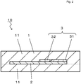
Fig. 2 is a cross-sectional view of the heater illustrated inFig. 1 taken along line A-A'. -
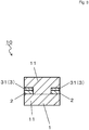
Fig. 3 is a cross-sectional view of the heater illustrated inFig. 1 taken along line B-B'. -
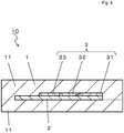
Fig. 4 is a cross-sectional view of a modification of the heater. -
Fig. 5 is a perspective view of an ignition device including the heater illustrated inFig. 1 . - A
heater 10 will be described with reference to the drawings. - As illustrated in
Figs. 1 to 3 , theheater 10 includes aceramic multilayer body 1 including a plurality ofceramic layers 11 that are stacked together, a heat-generatingresistor 2 provided between the adjacentceramic layers 11, andconductive layers 3 stacked on the heat-generatingresistor 2. Theheater 10 may be used in, for example, a glow plug of an automobile engine or a gas stove. - The
ceramic multilayer body 1 is a member in which the heat-generatingresistor 2 and theconductive layers 3 are embedded. The durabilities of the heat-generatingresistor 2 and theconductive layers 3 can be increased by placing the heat-generatingresistor 2 and theconductive layers 3 in theceramic multilayer body 1. Theceramic multilayer body 1 is, for example, a rod-shaped or plate-shaped member. - The
ceramic multilayer body 1 is made of an electrically insulative ceramic, such as an insulating ceramic, a nitride ceramic, or a carbide ceramic. More specifically, theceramic multilayer body 1 is made of, for example, an alumina ceramic, a silicon nitride ceramic, an aluminum nitride ceramic, or a silicon carbide ceramic. - The
ceramic multilayer body 1 made of a silicon nitride ceramic may be obtained by the following method. For example, silicon nitride, which is the main component, is mixed with 5 to 15 mass% of rare earth oxide, such as Y2O3, Yb2O3, or Er2O3, which functions as a sintering additive; 0.5 to 5 mass% of Al2O3; and SiO2, the amount of which is adjusted so that the amount of SiO2 in the sintered body is 1.5 to 5 mass%. The thus-obtained material is formed in a predetermined shape, and is then fired at a temperature of 1650°C to 1780°C. Thus, theceramic multilayer body 1 made of a silicon nitride ceramic is obtained. Hot press firing, for example, may be performed in the firing process. - When the
ceramic multilayer body 1 is rod-shaped, more specifically, rectangular-prism-shaped, the length of theceramic multilayer body 1 is set to, for example, 20 to 100 mm. The cross-sectional shape of theceramic multilayer body 1 is set to, for example, a rectangle having a thickness of 1 to 6 mm and a width of 2 to 40 mm. - The heat-generating
resistor 2 is a layer-shaped member that generates heat when a voltage is applied thereto. The heat-generatingresistor 2 is disposed between the adjacentceramic layers 11. When a voltage is applied to the heat-generatingresistor 2, a current flows through the heat-generatingresistor 2, and the heat-generatingresistor 2 generates heat. The generated heat is transferred through theceramic multilayer body 1, so that the temperature of the surface of theceramic multilayer body 1 increases. The heat is transferred from the surface of theceramic multilayer body 1 to an object to be heated, thereby providing the function of theheater 10. The object to be heated that receives the heat from the surface of theceramic multilayer body 1 is, for example, diesel oil to be supplied to an automobile diesel engine. - The heat-generating
resistor 2 is arranged in such a manner that both ends thereof are at a side surface of theceramic multilayer body 1 near the rear end of theceramic multilayer body 1. The heat-generatingresistor 2 has, for example, a bent shape in longitudinal cross section (cross section parallel to the length direction of the heat-generating resistor 2). More specifically, the heat-generatingresistor 2 includes two linear portions that are arranged next to each other and a connecting portion that has substantially semicircular or substantially semielliptical inner and outer peripheries and that is bent so as to connect the two linear portions. The heat-generatingresistor 2 is bent at a location near the front end of theceramic multilayer body 1. The total length of the heat-generatingresistor 2 is, for example, 35 to 100 mm. - The heat-generating
resistor 2 is designed so as to generate a large amount of heat in a region near the front end of theceramic multilayer body 1. More specifically, theconductive layers 3 are stacked on both end portions of the heat-generatingresistor 2 in a region near the rear end of theceramic multilayer body 1. Accordingly, a current flows through both the heat-generatingresistor 2 and theconductive layers 3 in the region near the rear end of theceramic multilayer body 1. As a result, the amount of heat generated by the heat-generatingresistor 2 is small in the region near the rear end of theceramic multilayer body 1. In contrast, the current flows only through the heat-generatingresistor 2 in the region near the front end of theceramic multilayer body 1. As a result, the amount of heat generated by the heat-generatingresistor 2 is large in the region near the front end of theceramic multilayer body 1. - The heat-generating
resistor 2 is made of, for example, a material having a carbide, nitride, silicide, etc., of tungsten (W), molybdenum (Mo), titanium (Ti), etc., as the main component. When theceramic multilayer body 1 is made of a silicon nitride ceramic, the heat-generatingresistor 2 is preferably made of a material having tungsten carbide as the main component. In this case, the coefficient of thermal expansion of theceramic multilayer body 1 and that of the heat-generatingresistor 2 can be made close to each other. - The
conductive layers 3 are members for adjusting the amount of heat generated by the heat-generatingresistor 2 in the region near the rear end of theceramic multilayer body 1, that is, in the region around the portions of the side surface of theceramic multilayer body 1 to which the heat-generatingresistor 2 extends. InFig. 1 , theconductive layers 3 are shown by the broken lines. InFig. 1 , the broken lines that show theconductive layers 3 and the solid lines that show the heat-generatingresistor 2 are shifted from each other to improve visibility. However, in practice, theconductive layers 3 and the heat-generatingresistor 2 have substantially the same width, and are stacked together so as to be aligned with each other in the width direction. As illustrated inFigs. 2 and3 , theconductive layers 3 are stacked on both end portions of the heat-generatingresistor 2 in the space between theceramic layers 11, and are arranged such that one end of eachconductive layer 3 is at the side surface of theceramic multilayer body 1. By covering both end portions of the heat-generatingresistor 2, which are to be connected to an external circuit, with theconductive layers 3, the amount of heat generated in the region near the rear end of theceramic multilayer body 1 can be reduced. Accordingly, the connection reliability between the external circuit and theheater 10 can be increased. - Each
conductive layer 3 includes a firstconductive layer 31 that extends to the side surface of theceramic multilayer body 1 and a secondconductive layer 32 that is adjacent to the firstconductive layer 31. The firstconductive layer 31 and the secondconductive layer 32 are each formed of a plurality of grains. The average grain diameter of the grains of the firstconductive layer 31 is smaller than that of the grains of the secondconductive layer 32. Since the firstconductive layer 31, which is located closer to the outside, is formed of grains having a small average grain diameter, the density of the firstconductive layer 31 can be increased. As a result, the voidage of the firstconductive layer 31 is reduced, and the risk that the outside air will flow into eachconductive layer 3 can be reduced. - Since not only the
conductive layers 3 but also the heat-generatingresistor 2 extends to the side surface of theceramic multilayer body 1, portions that extend to the side surface have a two-layer structure. Therefore, even when cracks are formed either in theconductive layers 3 or in the heat-generatingresistor 2, the risk that the cracks will extend into the other of theconductive layers 3 and the heat-generatingresistor 2 can be reduced. - Since the second
conductive layer 32 is formed of grains having a large average grain diameter, the number of grain boundaries of the grains of the secondconductive layers 32 can be reduced. Therefore, the resistance of the secondconductive layer 32 can be reduced. Accordingly, unnecessary heat generation by eachconductive layer 3 can be suppressed. - As a result, the long-term reliability of the
heater 10 when used in a heat cycle is increased. - More specifically, for example, in the case where conductive layers having a constant average grain diameter in each portion thereof are provided, unlike the above-described
heater 10, the following problem arises. That is, when the average grain diameter of the conductive layers is simply reduced, even though the risk that the outside air will flow into the conductive layers can be reduced, since the resistance of the conductive layers increases, unnecessary heat generation by the conductive layers occurs. Conversely, when the average grain diameter of the conductive layers is simply increased, even though unnecessarily heat generation by the conductive layers can be suppressed, the outside air easily flows into the conductive layers. In contrast, by making the average grain diameter of the grains of the firstconductive layer 31 smaller than that of the grains of the secondconductive layer 32 as in the above-describedheater 10, the risk that the outside air will enter eachconductive layer 3 can be reduced and unnecessary heat generation by eachconductive layer 3 can be suppressed. - In addition, as illustrated in
Fig. 2 , the firstconductive layer 31 and the secondconductive layer 32 preferably partially overlap. In such a case, unlike the case in which the firstconductive layer 31 and the secondconductive layer 32 do not overlap, eachconductive layer 3 can be formed so as to have a coefficient of thermal expansion that changes gradually in the length direction thereof. As a result, the possibility that cracks will be formed in theconductive layers 3 in a heat cycle can be reduced. - Preferably, the first
conductive layer 31 is located between the secondconductive layer 32 and the heat-generatingresistor 2, and, in a region in which the firstconductive layer 31 is located between the secondconductive layer 32 and the heat-generatingresistor 2, the firstconductive layer 31 has a thickness that decreases toward the other end thereof. In such a case, eachconductive layer 3 can be formed so as to have a coefficient of thermal expansion that changes smoothly. As a result, the possibility that cracks will be formed in theconductive layers 3 in a heat cycle can be further reduced. - In the above-described
heater 10, eachconductive layer 3 includes only the firstconductive layer 31 and the secondconductive layer 32. However, eachconductive layer 3 is not limited to this, and may further include a portion other than the firstconductive layer 31 and the secondconductive layer 32. For example, as illustrated inFig. 4 , eachconductive layer 3 may include, in addition to the firstconductive layer 31 and the secondconductive layer 32, a thirdconductive layer 33. The thirdconductive layer 33 is adjacent to the secondconductive layer 32 at a side opposite to the side adjacent to the firstconductive layer 31. - There is no particular limitation regarding the layer used as the third
conductive layer 33. For example, the thirdconductive layer 33 may be formed of grains having an average grain diameter smaller than that of the grains of the secondconductive layer 32. In such a case, the number of crystal grain boundaries of the grains of the thirdconductive layer 33 can be increased. Accordingly, the resistance of the thirdconductive layer 33 can be set to a value higher than that of the secondconductive layer 32. Therefore, the amount of heat generated by the heat-generatingresistor 2 can be changed gradually. Accordingly, the surface of theheater 10 can be heated in such a manner that the temperature thereof changes gradually. As a result, the risk that a large local thermal stress will be generated in theceramic multilayer body 1 can be reduced. - The first to third
conductive layers 31 to 33 are made of, for example, a highly heat-resistant metal material, such as molybdenum (Mo), tungsten (W), or rhenium (Re). MoSi2, WSi2, etc., are preferably mixed in the material to make the coefficient of thermal expansion close to that of theceramic multilayer body 1. The length of a portion of the firstconductive layer 31 that extends in the length direction of the heat-generatingresistor 2 is set to about 2 to 10 mm. The thickness of the firstconductive layer 31 is set to about 5 to 30 µm. The length of a portion of the secondconductive layer 32 that extends in the length direction of the heat-generatingresistor 2 is set to about 5 to 20 mm. The thickness of the secondconductive layer 32 is set to about 25 to 75 µm. In the case where the firstconductive layer 31 and the secondconductive layer 32 overlap, the length of the overlapping region is set to, for example, about 500 µm. - The grain diameters of the first
conductive layer 31 and the secondconductive layer 32 can be adjusted as follows. In the case where the firstconductive layer 31 and the secondconductive layer 32 are both made of W, the grain diameters of the firstconductive layer 31 and the secondconductive layer 32 can be adjusted by changing the particle diameter of W powder, which is the starting material. For example, the average grain diameter of the W powder used to form the firstconductive layer 31 may be set to 0.2 µm, and the average grain diameter of the W powder used to form the secondconductive layer 32 may be set to 1.2 µm. In this case, the average grain diameter of the firstconductive layer 31 can be set to 0.2 to 2 µm, and the average grain diameter of the secondconductive layer 32 can be set to 1.2 to 12 µm. - In particular, the average grain diameter of the first
conductive layer 31 is preferably less than 1 µm. In such a case, entrance of the outside air into the firstconductive layer 31 through the spaces between the grains can be suppressed, and therefore the risk that the outside air will flow into the firstconductive layer 31 can be reduced. The voidage of the first conductive layer is preferably less than 20%. In such a case, entrance of the outside air into the firstconductive layer 31 can be suppressed. - The average grain diameter of each
conductive layer 3 can be determined by, for example, the following method. That is, theheater 10 is cut along a plane that passes through theconductive layer 3 and that is perpendicular to theconductive layer 3 by using a diamond cutter. Then, the cut surface is ground by using diamond powder. After that, the firstconductive layer 31 and the secondconductive layer 32 are observed by using a scanning electron microscope or metallographic microscope. More specifically, five arbitrary straight lines are drawn on the image obtained by the scanning electron microscope or metallographic microscope. Then, the average of the lengths of portions of the five straight lines, each portion passing through ten grains, is determined. The average grain diameter is determined by dividing the average by ten, which is the number of grains. The average grain diameter may instead be calculated by using an image analyzing device (LUZEX-FS produced by Nireco Corporation). This image analyzing device can also be used to measure the voidage of the firstconductive layer 31. - The
heater 10 is used in, for example, anignition device 100 illustrated inFig. 5 . Theignition device 100 includes theheater 10 and achannel 20 through which fuel gas is supplied to theheater 10. Thechannel 20 includes, for example, agas valve 21 and agas flow pipe 22 having ejection holes 23. Thegas valve 21 has a function of controlling the flow rate of the fuel gas. The fuel gas supplied from thegas valve 21 is, for example, natural gas or propane gas. Thegas flow pipe 22 ejects the fuel gas, which is supplied from thegas valve 21, toward theheater 10 through the ejection holes 23. The ejected fuel gas can be ignited by heating the fuel gas with theheater 10. Theignition device 100, which includes theheater 10 having improved long-term reliability, has increased fuel-gas ignition stability. -
- 1
- ceramic multilayer body
- 11
- ceramic layer
- 2
- heat-generating resistor
- 3
- conductive layer
- 31
- first conductive layer
- 32
- second conductive layer
- 10
- heater
- 20
- channel
- 21
- gas valve
- 22
- gas flow pipe
- 23
- ejection hole
- 100
- ignition device
Claims (6)
- A heater comprising:a ceramic multilayer body comprising a plurality of ceramic layers that are stacked together;a heat-generating resistor having a belt shape, the heat-generating resistor being disposed between the ceramic layers and arranged, and comprising both ends that are at a side surface of the ceramic multilayer body; andconductive layers having a belt shape, disposed between the ceramic layers and stacked on both end portions of the heat-generating resistor in such a manner that one end of each conductive layer is at the side surface;wherein each conductive layer comprises a first conductive layer that extends to the side surface and a second conductive layer that is adjacent to the first conductive layer, each of the first conductive layer and the second conductive layer being formed of a plurality of grains, the grains of the first conductive layer having an average grain diameter smaller than an average grain diameter of the grains of the second conductive layer.
- The heater according to Claim 1, wherein the first conductive layer and the second conductive layer partially overlap.
- The heater according to Claim 2, wherein, in a region in which the first conductive layer and the second conductive layer overlap, the first conductive layer is located between the second conductive layer and the heat-generating resistor, and
wherein, in a region in which the first conductive layer is located between the second conductive layer and the heat-generating resistor, the first conductive layer has a thickness that decreases toward the other end of the first conductive layer. - The heater according to any one of Claims 1 to 3,
wherein the grains of the first conductive layer have an average grain diameter of 0.2 to 2 µm, and the grains of the second conductive layer have an average grain diameter of 1.2 to 12 µm. - The heater according to any one of Claims 1 to 4,
wherein the first conductive layer has a voidage of less than 20%. - An ignition device comprising:the heater according to any one of Claims 1 to 5; anda channel through which fuel gas flows to the ceramic multilayer body included in the heater.
Applications Claiming Priority (2)
| Application Number | Priority Date | Filing Date | Title |
|---|---|---|---|
| JP2014090911 | 2014-04-25 | ||
| PCT/JP2015/062651 WO2015163483A1 (en) | 2014-04-25 | 2015-04-27 | Heater and ignition device |
Publications (3)
| Publication Number | Publication Date |
|---|---|
| EP3136819A1 true EP3136819A1 (en) | 2017-03-01 |
| EP3136819A4 EP3136819A4 (en) | 2017-12-27 |
| EP3136819B1 EP3136819B1 (en) | 2020-05-06 |
Family
ID=54332639
Family Applications (1)
| Application Number | Title | Priority Date | Filing Date |
|---|---|---|---|
| EP15782910.2A Active EP3136819B1 (en) | 2014-04-25 | 2015-04-27 | Heater and ignition device |
Country Status (4)
| Country | Link |
|---|---|
| EP (1) | EP3136819B1 (en) |
| JP (1) | JP6027289B2 (en) |
| CN (1) | CN106105384B (en) |
| WO (1) | WO2015163483A1 (en) |
Cited By (1)
| Publication number | Priority date | Publication date | Assignee | Title |
|---|---|---|---|---|
| WO2021034748A1 (en) * | 2019-08-19 | 2021-02-25 | Scp Holdings, An Assumed Business Name Of Nitride Igniters, Llc. | Thermally-actuated gas valve with ceramic heater |
Families Citing this family (1)
| Publication number | Priority date | Publication date | Assignee | Title |
|---|---|---|---|---|
| JP6987995B2 (en) * | 2018-07-31 | 2022-01-05 | 京セラ株式会社 | heater |
Family Cites Families (17)
| Publication number | Priority date | Publication date | Assignee | Title |
|---|---|---|---|---|
| JPH01272078A (en) * | 1988-04-21 | 1989-10-31 | Rinnai Corp | Ceramic heater |
| JP2537271B2 (en) * | 1988-09-09 | 1996-09-25 | 日本特殊陶業株式会社 | Ceramic heating element |
| JPH0429192U (en) * | 1990-07-02 | 1992-03-09 | ||
| JP3121860B2 (en) * | 1991-06-06 | 2001-01-09 | 京セラ株式会社 | Ceramic heater |
| JP2828575B2 (en) * | 1993-11-12 | 1998-11-25 | 京セラ株式会社 | Silicon nitride ceramic heater |
| DE19731900A1 (en) * | 1997-07-24 | 1999-02-11 | Heraeus Electro Nite Int | Conductive layer with variable electrical resistance, process for its manufacture and use |
| JP3691649B2 (en) * | 1997-10-28 | 2005-09-07 | 日本特殊陶業株式会社 | Ceramic heater |
| JP2001244053A (en) * | 2000-02-29 | 2001-09-07 | Tdk Corp | Resistive element for heating |
| JP3924193B2 (en) * | 2001-05-02 | 2007-06-06 | 日本特殊陶業株式会社 | Ceramic heater, glow plug using the same, and method for manufacturing ceramic heater |
| WO2005060311A1 (en) * | 2003-11-25 | 2005-06-30 | Kyocera Corporation | Ceramic heater and method for manufacture thereof |
| JP4183186B2 (en) * | 2004-03-29 | 2008-11-19 | 京セラ株式会社 | Ceramic heater |
| KR20080108372A (en) * | 2003-12-24 | 2008-12-12 | 쿄세라 코포레이션 | Ceramic heater and its manufacturing method |
| EP2117280B1 (en) * | 2007-02-22 | 2018-04-11 | Kyocera Corporation | Ceramic heater, glow plug using the ceramic heater, and ceramic heater manufacturing method |
| JP5357628B2 (en) * | 2009-05-26 | 2013-12-04 | 日本特殊陶業株式会社 | Manufacturing method of ceramic heater |
| JP5721584B2 (en) * | 2011-08-10 | 2015-05-20 | 京セラ株式会社 | Heater and glow plug equipped with the same |
| US9491804B2 (en) * | 2011-09-29 | 2016-11-08 | Kyocera Corporation | Heater and glow plug including the same |
| CN105165113B (en) * | 2013-04-27 | 2017-06-23 | 京瓷株式会社 | Ceramic heater |
-
2015
- 2015-04-27 CN CN201580012328.8A patent/CN106105384B/en active Active
- 2015-04-27 JP JP2016515248A patent/JP6027289B2/en active Active
- 2015-04-27 EP EP15782910.2A patent/EP3136819B1/en active Active
- 2015-04-27 WO PCT/JP2015/062651 patent/WO2015163483A1/en not_active Ceased
Cited By (2)
| Publication number | Priority date | Publication date | Assignee | Title |
|---|---|---|---|---|
| WO2021034748A1 (en) * | 2019-08-19 | 2021-02-25 | Scp Holdings, An Assumed Business Name Of Nitride Igniters, Llc. | Thermally-actuated gas valve with ceramic heater |
| EP4018127A4 (en) * | 2019-08-19 | 2023-03-01 | SCP Holdings, an Assumed Business Name of Nitride Igniters, LLC. | Thermally-actuated gas valve with ceramic heater |
Also Published As
| Publication number | Publication date |
|---|---|
| EP3136819A4 (en) | 2017-12-27 |
| JPWO2015163483A1 (en) | 2017-04-20 |
| CN106105384B (en) | 2019-08-02 |
| EP3136819B1 (en) | 2020-05-06 |
| WO2015163483A1 (en) | 2015-10-29 |
| JP6027289B2 (en) | 2016-11-16 |
| CN106105384A (en) | 2016-11-09 |
Similar Documents
| Publication | Publication Date | Title |
|---|---|---|
| CN105165113B (en) | Ceramic heater | |
| JP6247375B2 (en) | Heater and glow plug equipped with the same | |
| EP3136819B1 (en) | Heater and ignition device | |
| JPWO2011065366A1 (en) | Ceramic heater | |
| EP2693834B1 (en) | Heater | |
| US9291144B2 (en) | Heater and glow plug including the same | |
| EP2914057B1 (en) | Heater and glow plug equipped with same | |
| EP2704518B1 (en) | Heater and glow plug provided with same | |
| JP5721584B2 (en) | Heater and glow plug equipped with the same | |
| EP3151630B1 (en) | Ceramic heater and ignition device provided with same | |
| JP6957663B2 (en) | Ceramic heater | |
| JP5944815B2 (en) | Heater and glow plug equipped with the same | |
| JP5864301B2 (en) | Heater and glow plug equipped with the same | |
| JP6224797B2 (en) | Heater and glow plug equipped with the same | |
| EP3106754B1 (en) | Ceramic heater and glow plug | |
| JP6952395B2 (en) | heater | |
| JP6673644B2 (en) | Ceramic heater | |
| JP6483512B2 (en) | Heater and glow plug equipped with the same | |
| JP6272519B2 (en) | Heater and glow plug equipped with the same | |
| JP6085050B2 (en) | Heater and glow plug equipped with the same | |
| JP5909573B2 (en) | Heater and glow plug equipped with the same | |
| JP2016040787A (en) | Heater and glow plug equipped with the same | |
| JPWO2017038694A1 (en) | Heater and glow plug equipped with the same | |
| JP2016015342A (en) | Heater and glow plug equipped with the same |
Legal Events
| Date | Code | Title | Description |
|---|---|---|---|
| STAA | Information on the status of an ep patent application or granted ep patent |
Free format text: STATUS: THE INTERNATIONAL PUBLICATION HAS BEEN MADE |
|
| PUAI | Public reference made under article 153(3) epc to a published international application that has entered the european phase |
Free format text: ORIGINAL CODE: 0009012 |
|
| STAA | Information on the status of an ep patent application or granted ep patent |
Free format text: STATUS: REQUEST FOR EXAMINATION WAS MADE |
|
| 17P | Request for examination filed |
Effective date: 20160909 |
|
| AK | Designated contracting states |
Kind code of ref document: A1 Designated state(s): AL AT BE BG CH CY CZ DE DK EE ES FI FR GB GR HR HU IE IS IT LI LT LU LV MC MK MT NL NO PL PT RO RS SE SI SK SM TR |
|
| AX | Request for extension of the european patent |
Extension state: BA ME |
|
| DAV | Request for validation of the european patent (deleted) | ||
| DAX | Request for extension of the european patent (deleted) | ||
| A4 | Supplementary search report drawn up and despatched |
Effective date: 20171127 |
|
| RIC1 | Information provided on ipc code assigned before grant |
Ipc: H05B 3/48 20060101ALI20171121BHEP Ipc: H05B 3/14 20060101ALI20171121BHEP Ipc: H05B 3/18 20060101ALI20171121BHEP Ipc: H05B 3/06 20060101ALI20171121BHEP Ipc: H05B 3/12 20060101ALI20171121BHEP Ipc: H05B 3/02 20060101AFI20171121BHEP |
|
| GRAP | Despatch of communication of intention to grant a patent |
Free format text: ORIGINAL CODE: EPIDOSNIGR1 |
|
| STAA | Information on the status of an ep patent application or granted ep patent |
Free format text: STATUS: GRANT OF PATENT IS INTENDED |
|
| INTG | Intention to grant announced |
Effective date: 20191220 |
|
| GRAS | Grant fee paid |
Free format text: ORIGINAL CODE: EPIDOSNIGR3 |
|
| GRAA | (expected) grant |
Free format text: ORIGINAL CODE: 0009210 |
|
| STAA | Information on the status of an ep patent application or granted ep patent |
Free format text: STATUS: THE PATENT HAS BEEN GRANTED |
|
| AK | Designated contracting states |
Kind code of ref document: B1 Designated state(s): AL AT BE BG CH CY CZ DE DK EE ES FI FR GB GR HR HU IE IS IT LI LT LU LV MC MK MT NL NO PL PT RO RS SE SI SK SM TR |
|
| REG | Reference to a national code |
Ref country code: GB Ref legal event code: FG4D |
|
| REG | Reference to a national code |
Ref country code: CH Ref legal event code: EP Ref country code: AT Ref legal event code: REF Ref document number: 1268920 Country of ref document: AT Kind code of ref document: T Effective date: 20200515 |
|
| REG | Reference to a national code |
Ref country code: DE Ref legal event code: R096 Ref document number: 602015052336 Country of ref document: DE |
|
| REG | Reference to a national code |
Ref country code: IE Ref legal event code: FG4D |
|
| REG | Reference to a national code |
Ref country code: LT Ref legal event code: MG4D |
|
| REG | Reference to a national code |
Ref country code: NL Ref legal event code: MP Effective date: 20200506 |
|
| PG25 | Lapsed in a contracting state [announced via postgrant information from national office to epo] |
Ref country code: IS Free format text: LAPSE BECAUSE OF FAILURE TO SUBMIT A TRANSLATION OF THE DESCRIPTION OR TO PAY THE FEE WITHIN THE PRESCRIBED TIME-LIMIT Effective date: 20200906 Ref country code: GR Free format text: LAPSE BECAUSE OF FAILURE TO SUBMIT A TRANSLATION OF THE DESCRIPTION OR TO PAY THE FEE WITHIN THE PRESCRIBED TIME-LIMIT Effective date: 20200807 Ref country code: NO Free format text: LAPSE BECAUSE OF FAILURE TO SUBMIT A TRANSLATION OF THE DESCRIPTION OR TO PAY THE FEE WITHIN THE PRESCRIBED TIME-LIMIT Effective date: 20200806 Ref country code: LT Free format text: LAPSE BECAUSE OF FAILURE TO SUBMIT A TRANSLATION OF THE DESCRIPTION OR TO PAY THE FEE WITHIN THE PRESCRIBED TIME-LIMIT Effective date: 20200506 Ref country code: SE Free format text: LAPSE BECAUSE OF FAILURE TO SUBMIT A TRANSLATION OF THE DESCRIPTION OR TO PAY THE FEE WITHIN THE PRESCRIBED TIME-LIMIT Effective date: 20200506 Ref country code: FI Free format text: LAPSE BECAUSE OF FAILURE TO SUBMIT A TRANSLATION OF THE DESCRIPTION OR TO PAY THE FEE WITHIN THE PRESCRIBED TIME-LIMIT Effective date: 20200506 Ref country code: PT Free format text: LAPSE BECAUSE OF FAILURE TO SUBMIT A TRANSLATION OF THE DESCRIPTION OR TO PAY THE FEE WITHIN THE PRESCRIBED TIME-LIMIT Effective date: 20200907 |
|
| PG25 | Lapsed in a contracting state [announced via postgrant information from national office to epo] |
Ref country code: HR Free format text: LAPSE BECAUSE OF FAILURE TO SUBMIT A TRANSLATION OF THE DESCRIPTION OR TO PAY THE FEE WITHIN THE PRESCRIBED TIME-LIMIT Effective date: 20200506 Ref country code: LV Free format text: LAPSE BECAUSE OF FAILURE TO SUBMIT A TRANSLATION OF THE DESCRIPTION OR TO PAY THE FEE WITHIN THE PRESCRIBED TIME-LIMIT Effective date: 20200506 Ref country code: RS Free format text: LAPSE BECAUSE OF FAILURE TO SUBMIT A TRANSLATION OF THE DESCRIPTION OR TO PAY THE FEE WITHIN THE PRESCRIBED TIME-LIMIT Effective date: 20200506 Ref country code: BG Free format text: LAPSE BECAUSE OF FAILURE TO SUBMIT A TRANSLATION OF THE DESCRIPTION OR TO PAY THE FEE WITHIN THE PRESCRIBED TIME-LIMIT Effective date: 20200806 |
|
| REG | Reference to a national code |
Ref country code: AT Ref legal event code: MK05 Ref document number: 1268920 Country of ref document: AT Kind code of ref document: T Effective date: 20200506 |
|
| PG25 | Lapsed in a contracting state [announced via postgrant information from national office to epo] |
Ref country code: AL Free format text: LAPSE BECAUSE OF FAILURE TO SUBMIT A TRANSLATION OF THE DESCRIPTION OR TO PAY THE FEE WITHIN THE PRESCRIBED TIME-LIMIT Effective date: 20200506 Ref country code: NL Free format text: LAPSE BECAUSE OF FAILURE TO SUBMIT A TRANSLATION OF THE DESCRIPTION OR TO PAY THE FEE WITHIN THE PRESCRIBED TIME-LIMIT Effective date: 20200506 |
|
| PG25 | Lapsed in a contracting state [announced via postgrant information from national office to epo] |
Ref country code: DK Free format text: LAPSE BECAUSE OF FAILURE TO SUBMIT A TRANSLATION OF THE DESCRIPTION OR TO PAY THE FEE WITHIN THE PRESCRIBED TIME-LIMIT Effective date: 20200506 Ref country code: ES Free format text: LAPSE BECAUSE OF FAILURE TO SUBMIT A TRANSLATION OF THE DESCRIPTION OR TO PAY THE FEE WITHIN THE PRESCRIBED TIME-LIMIT Effective date: 20200506 Ref country code: CZ Free format text: LAPSE BECAUSE OF FAILURE TO SUBMIT A TRANSLATION OF THE DESCRIPTION OR TO PAY THE FEE WITHIN THE PRESCRIBED TIME-LIMIT Effective date: 20200506 Ref country code: RO Free format text: LAPSE BECAUSE OF FAILURE TO SUBMIT A TRANSLATION OF THE DESCRIPTION OR TO PAY THE FEE WITHIN THE PRESCRIBED TIME-LIMIT Effective date: 20200506 Ref country code: IT Free format text: LAPSE BECAUSE OF FAILURE TO SUBMIT A TRANSLATION OF THE DESCRIPTION OR TO PAY THE FEE WITHIN THE PRESCRIBED TIME-LIMIT Effective date: 20200506 Ref country code: SM Free format text: LAPSE BECAUSE OF FAILURE TO SUBMIT A TRANSLATION OF THE DESCRIPTION OR TO PAY THE FEE WITHIN THE PRESCRIBED TIME-LIMIT Effective date: 20200506 Ref country code: AT Free format text: LAPSE BECAUSE OF FAILURE TO SUBMIT A TRANSLATION OF THE DESCRIPTION OR TO PAY THE FEE WITHIN THE PRESCRIBED TIME-LIMIT Effective date: 20200506 Ref country code: EE Free format text: LAPSE BECAUSE OF FAILURE TO SUBMIT A TRANSLATION OF THE DESCRIPTION OR TO PAY THE FEE WITHIN THE PRESCRIBED TIME-LIMIT Effective date: 20200506 |
|
| REG | Reference to a national code |
Ref country code: DE Ref legal event code: R097 Ref document number: 602015052336 Country of ref document: DE |
|
| PG25 | Lapsed in a contracting state [announced via postgrant information from national office to epo] |
Ref country code: PL Free format text: LAPSE BECAUSE OF FAILURE TO SUBMIT A TRANSLATION OF THE DESCRIPTION OR TO PAY THE FEE WITHIN THE PRESCRIBED TIME-LIMIT Effective date: 20200506 Ref country code: SK Free format text: LAPSE BECAUSE OF FAILURE TO SUBMIT A TRANSLATION OF THE DESCRIPTION OR TO PAY THE FEE WITHIN THE PRESCRIBED TIME-LIMIT Effective date: 20200506 |
|
| PLBE | No opposition filed within time limit |
Free format text: ORIGINAL CODE: 0009261 |
|
| STAA | Information on the status of an ep patent application or granted ep patent |
Free format text: STATUS: NO OPPOSITION FILED WITHIN TIME LIMIT |
|
| 26N | No opposition filed |
Effective date: 20210209 |
|
| PG25 | Lapsed in a contracting state [announced via postgrant information from national office to epo] |
Ref country code: SI Free format text: LAPSE BECAUSE OF FAILURE TO SUBMIT A TRANSLATION OF THE DESCRIPTION OR TO PAY THE FEE WITHIN THE PRESCRIBED TIME-LIMIT Effective date: 20200506 |
|
| PG25 | Lapsed in a contracting state [announced via postgrant information from national office to epo] |
Ref country code: MC Free format text: LAPSE BECAUSE OF FAILURE TO SUBMIT A TRANSLATION OF THE DESCRIPTION OR TO PAY THE FEE WITHIN THE PRESCRIBED TIME-LIMIT Effective date: 20200506 |
|
| PG25 | Lapsed in a contracting state [announced via postgrant information from national office to epo] |
Ref country code: LU Free format text: LAPSE BECAUSE OF NON-PAYMENT OF DUE FEES Effective date: 20210427 |
|
| REG | Reference to a national code |
Ref country code: BE Ref legal event code: MM Effective date: 20210430 |
|
| PG25 | Lapsed in a contracting state [announced via postgrant information from national office to epo] |
Ref country code: LI Free format text: LAPSE BECAUSE OF NON-PAYMENT OF DUE FEES Effective date: 20210430 Ref country code: CH Free format text: LAPSE BECAUSE OF NON-PAYMENT OF DUE FEES Effective date: 20210430 |
|
| PG25 | Lapsed in a contracting state [announced via postgrant information from national office to epo] |
Ref country code: IE Free format text: LAPSE BECAUSE OF NON-PAYMENT OF DUE FEES Effective date: 20210427 |
|
| PG25 | Lapsed in a contracting state [announced via postgrant information from national office to epo] |
Ref country code: BE Free format text: LAPSE BECAUSE OF NON-PAYMENT OF DUE FEES Effective date: 20210430 |
|
| PG25 | Lapsed in a contracting state [announced via postgrant information from national office to epo] |
Ref country code: HU Free format text: LAPSE BECAUSE OF FAILURE TO SUBMIT A TRANSLATION OF THE DESCRIPTION OR TO PAY THE FEE WITHIN THE PRESCRIBED TIME-LIMIT; INVALID AB INITIO Effective date: 20150427 |
|
| P01 | Opt-out of the competence of the unified patent court (upc) registered |
Effective date: 20230505 |
|
| PG25 | Lapsed in a contracting state [announced via postgrant information from national office to epo] |
Ref country code: CY Free format text: LAPSE BECAUSE OF FAILURE TO SUBMIT A TRANSLATION OF THE DESCRIPTION OR TO PAY THE FEE WITHIN THE PRESCRIBED TIME-LIMIT Effective date: 20200506 |
|
| PG25 | Lapsed in a contracting state [announced via postgrant information from national office to epo] |
Ref country code: MK Free format text: LAPSE BECAUSE OF FAILURE TO SUBMIT A TRANSLATION OF THE DESCRIPTION OR TO PAY THE FEE WITHIN THE PRESCRIBED TIME-LIMIT Effective date: 20200506 |
|
| PG25 | Lapsed in a contracting state [announced via postgrant information from national office to epo] |
Ref country code: TR Free format text: LAPSE BECAUSE OF FAILURE TO SUBMIT A TRANSLATION OF THE DESCRIPTION OR TO PAY THE FEE WITHIN THE PRESCRIBED TIME-LIMIT Effective date: 20200506 |
|
| PG25 | Lapsed in a contracting state [announced via postgrant information from national office to epo] |
Ref country code: MT Free format text: LAPSE BECAUSE OF FAILURE TO SUBMIT A TRANSLATION OF THE DESCRIPTION OR TO PAY THE FEE WITHIN THE PRESCRIBED TIME-LIMIT Effective date: 20200506 |
|
| PGFP | Annual fee paid to national office [announced via postgrant information from national office to epo] |
Ref country code: FR Payment date: 20250310 Year of fee payment: 11 |
|
| PGFP | Annual fee paid to national office [announced via postgrant information from national office to epo] |
Ref country code: GB Payment date: 20250306 Year of fee payment: 11 |
|
| PGFP | Annual fee paid to national office [announced via postgrant information from national office to epo] |
Ref country code: DE Payment date: 20250305 Year of fee payment: 11 |