EP3136506B1 - Kommunikationsvorrichtung - Google Patents
Kommunikationsvorrichtung Download PDFInfo
- Publication number
- EP3136506B1 EP3136506B1 EP15197643.8A EP15197643A EP3136506B1 EP 3136506 B1 EP3136506 B1 EP 3136506B1 EP 15197643 A EP15197643 A EP 15197643A EP 3136506 B1 EP3136506 B1 EP 3136506B1
- Authority
- EP
- European Patent Office
- Prior art keywords
- communication device
- antenna element
- radiation
- band
- electrically connected
- Prior art date
- Legal status (The legal status is an assumption and is not a legal conclusion. Google has not performed a legal analysis and makes no representation as to the accuracy of the status listed.)
- Not-in-force
Links
Images



Classifications
-
- H—ELECTRICITY
- H04—ELECTRIC COMMUNICATION TECHNIQUE
- H04M—TELEPHONIC COMMUNICATION
- H04M1/00—Substation equipment, e.g. for use by subscribers
- H04M1/02—Constructional features of telephone sets
- H04M1/0202—Portable telephone sets, e.g. cordless phones, mobile phones or bar type handsets
- H04M1/026—Details of the structure or mounting of specific components
-
- H—ELECTRICITY
- H01—ELECTRIC ELEMENTS
- H01Q—ANTENNAS, i.e. RADIO AERIALS
- H01Q1/00—Details of, or arrangements associated with, antennas
- H01Q1/12—Supports; Mounting means
- H01Q1/22—Supports; Mounting means by structural association with other equipment or articles
- H01Q1/24—Supports; Mounting means by structural association with other equipment or articles with receiving set
- H01Q1/241—Supports; Mounting means by structural association with other equipment or articles with receiving set used in mobile communications, e.g. GSM
- H01Q1/242—Supports; Mounting means by structural association with other equipment or articles with receiving set used in mobile communications, e.g. GSM specially adapted for hand-held use
- H01Q1/243—Supports; Mounting means by structural association with other equipment or articles with receiving set used in mobile communications, e.g. GSM specially adapted for hand-held use with built-in antennas
-
- H—ELECTRICITY
- H01—ELECTRIC ELEMENTS
- H01Q—ANTENNAS, i.e. RADIO AERIALS
- H01Q1/00—Details of, or arrangements associated with, antennas
- H01Q1/36—Structural form of radiating elements, e.g. cone, spiral, umbrella; Particular materials used therewith
- H01Q1/38—Structural form of radiating elements, e.g. cone, spiral, umbrella; Particular materials used therewith formed by a conductive layer on an insulating support
-
- H—ELECTRICITY
- H01—ELECTRIC ELEMENTS
- H01Q—ANTENNAS, i.e. RADIO AERIALS
- H01Q5/00—Arrangements for simultaneous operation of antennas on two or more different wavebands, e.g. dual-band or multi-band arrangements
- H01Q5/30—Arrangements for providing operation on different wavebands
- H01Q5/307—Individual or coupled radiating elements, each element being fed in an unspecified way
- H01Q5/342—Individual or coupled radiating elements, each element being fed in an unspecified way for different propagation modes
- H01Q5/357—Individual or coupled radiating elements, each element being fed in an unspecified way for different propagation modes using a single feed point
- H01Q5/364—Creating multiple current paths
-
- H—ELECTRICITY
- H01—ELECTRIC ELEMENTS
- H01Q—ANTENNAS, i.e. RADIO AERIALS
- H01Q9/00—Electrically-short antennas having dimensions not more than twice the operating wavelength and consisting of conductive active radiating elements
- H01Q9/04—Resonant antennas
- H01Q9/30—Resonant antennas with feed to end of elongated active element, e.g. unipole
- H01Q9/42—Resonant antennas with feed to end of elongated active element, e.g. unipole with folded element, the folded parts being spaced apart a small fraction of the operating wavelength
-
- H—ELECTRICITY
- H04—ELECTRIC COMMUNICATION TECHNIQUE
- H04B—TRANSMISSION
- H04B1/00—Details of transmission systems, not covered by a single one of groups H04B3/00 - H04B13/00; Details of transmission systems not characterised by the medium used for transmission
- H04B1/38—Transceivers, i.e. devices in which transmitter and receiver form a structural unit and in which at least one part is used for functions of transmitting and receiving
- H04B1/3827—Portable transceivers
-
- H—ELECTRICITY
- H01—ELECTRIC ELEMENTS
- H01Q—ANTENNAS, i.e. RADIO AERIALS
- H01Q7/00—Loop antennas with a substantially uniform current distribution around the loop and having a directional radiation pattern in a plane perpendicular to the plane of the loop
Definitions
- a communication device is provided, which reduces space occupied by a first radiation portion and a second radiation portion in the Y-axis direction so that an antenna element has a low-profile characteristic.
- FIG. 1 is a schematic diagram of a communication device according to an embodiment of the invention.
- a communication device 10 includes a ground plane 11, an antenna element 12 and a substrate 110.
- the ground plane 11 and the antenna element 12 are disposed on a surface 111 of the substrate 110, and the substrate 110 may be, for example, a printed circuit board.
- the antenna element 12 may be, for example, a planar antenna, and the antenna element 12 includes a feeding portion 120, a first radiation portion 130, a second radiation portion 140 and an adjusting portion 150.
- the ground plane 11 includes a first edge SD11 and a second edge SD12 that are adjacent to each other.
- the feeding portion 120 is close to the first edge SD11 of the ground plane 11.
- the first radiation portion includes a first portion 131 and a second portion 132. A first end of the first portion 131 is electrically connected to the feeding portion 120. A first end of the second portion 132 is electrically connected to a second end of the first portion 131, and a second end of the second portion 132 is electrically connected to the second edge SD12 of the ground plane 11.
- the shape of the first portion 131 may be, for example, linear, and the shape of the second portion 132 may be, for example, inverted-L. Furthermore, the first portion 131 faces the second portion 132 and the first edge SD11 of the ground plane 11. The second portion 132 extends from the second edge SD12 of the ground plane 11. Thereby, the shape of the first radiation portion 130 is like an inverted U and has an opening towards a first direction (for example, -X-axis direction).
- a first end of the second radiation portion 140 is electrically connected to the feeding portion 120, and a second end of the second radiation portion 140 is an open end.
- the second radiation portion 140 includes a bend, so that part of the second radiation portion 140 is parallel to the first portion 131 of the first radiation portion 130.
- the shape of the second radiation portion 140 may be, for example, an inverted L, and the second radiation portion 140 and the first portion 131 may form an opening towards a second direction (for example, X-axis direction).
- the adjusting portion 150 is electrically connected between the first portion 131 and the second portion 132, and the adjusting portion 150 is parallel to part of the second portion 132.
- the feeding portion 120 and the first radiation portion 130 form a first resonant path
- the feeding portion 120 and the second radiation portion 140 form a second resonant path
- the antenna element 12 receives a feeding signal from a transceiver (not shown) in the communication device 10 through the feeding portion 120.
- the feeding portion 120 may be electrically connected to the transceiver through a coaxial cable 160, wherein an inner conductor of the coaxial cable 160 is electrically connected to the feeding portion 120, and an outer conductor of the coaxial cable 160 is electrically connected to the ground plane 11.
- FIGs. 2 and 3 are respectively schematic diagrams for illustrating operation of the antenna element according to an embodiment of the invention, and the operation of the antenna element is further described with reference to FIGs. 1 to 3 .
- the feeding portion 120 and the first radiation portion 130 form a first resonant path 210.
- the antenna element 12 When excited by the feeding signal, the antenna element 12 generates the first resonant mode through the first resonant path 210, so as to operate in the first band (for example, a low-frequency band).
- the first resonant path 210 has a loop structure. That is, the first radiation portion 130 has a loop antenna structure.
- the first resonant path 210 is 1/2 wavelength of the lowest frequency of the first band, and the antenna element 12 operating in the first band (for example, a low-frequency band) is less easily disturbed by external environments.
- the feeding portion 120 and the second radiation portion 140 form a second resonant path 310.
- the antenna element 12 When excited by the feeding signal, the antenna element 12 generates the second resonant mode through the second resonant path 310, so as to operate in the second band (for example, a high-frequency band).
- the second radiation portion 140 has a monopole antenna structure. That is, the second resonant path 310 is 1/4 wavelength of the lowest frequency of the second band.
- part of the first portion 131 and the adjusting portion 150 and part of the second portion 132 form a current-dividing path 320. That is, the adjusting portion 150 and part of the first radiation portion 130 form the current-dividing path 320.
- the adjusting portion 150 and part of the first radiation portion 130 are equivalent to an inductive element.
- the current-dividing path 320 has an inductive effect, and the inductive effect is used for reducing a capacitive effect between the second radiation portion 140 and the ground plane 11.
- the adjusting portion 150 and part of the first radiation portion 130 is used for adjusting the impedance of the antenna element 12 operating in the second band, so that the antenna element 12 has good impedance match in the second band.
- the inductive effect contributed by the current-dividing path 320 may be adjusted by changing the place where the adjusting portion 150 is disposed. For instance, as shown in FIG. 3 , based on the place where the adjusting portion 150 is disposed, the first portion 131 may be divided into a first segment 330 and a second segment 340.
- the first segment 330 is electrically connected to the feeding portion 120, and the second segment 340 is electrically connected to the second portion 132.
- the length of the first segment 330 is twice the length of the second segment 340.
- the ground plane 11 and the second portion 132 of the first radiation portion 130 are arranged in sequence along the X-axis direction, and the first portion 131 and second portion 132 of the first radiation portion 130 face each other. Thereby, the space occupied by the first radiation portion 130 in the Y-axis direction is effectively reduced, so that the height of the antenna element 12 in the Y-axis direction is reduced.
- the impedance of the antenna element 12 operating in the second band may be adjusted with the current-dividing path, the antenna element 12 is still able to maintain good radiation characteristics when the second radiation portion 140 is nearby the ground plane 11. Thereby, the space occupied by the second radiation portion 140 in the Y-axis direction is effectively reduced, so that the height of the antenna element 12 in the Y-axis direction is further reduced.
- the area occupied by the antenna element 12, the coaxial cable 160 and the ground plane 11 may be expressed by a height 101 and a width 102 in FIG. 1 .
- the height 101 in FIG. 1 includes a height of the antenna element 12 in the Y-axis direction.
- the first band and the second band covered by the antenna element 12 may be, for example, 2.4GHz and 5GHz
- the height 101 and the width 102 may be, for example, 4.5mm and 24mm.
- current antenna elements operable in 2.4GHz and 5GHz mostly have a height greater than 8mm.
- the antenna element 12 in FIG. 1 has the low-profile characteristic. That is, the communication device 10 has a low-profile antenna element 12, so as to be feasible for narrow-frame designs.
- FIGs. 4 and 5 are respectively schematic diagrams of the appearance of a communication device according to an embodiment of the invention.
- the communication device 10 further includes a first body 410 and a second body 420, and a display 430 and a narrow frame 440 are disposed on the front surface of the first body 410, and a keyboard 450 is disposed on the front surface of the second body 420.
- the first body 410 may be unfolded with respect to the second body 420, so that there is an included angle between the front surface of the first body 410 and the front surface of the second body 420.
- the communication device 10 when the included angle between the front surface of the first body 410 and the front surface of the second body 420 is greater than 0 but smaller than 180, the communication device 10 is in a notebook mode.
- the antenna element 12 in FIG. 1 may be disposed in the first body 410 and face the narrow frame 440 surrounding the display 430. In other words, the antenna element 12 in the communication device 10 is disposed with respect to the narrow frame 440 of the display 430.
- the antenna element 12 since the antenna element 12 has the low-profile characteristic, the antenna element 12 matches the design needs for the display 430 having the narrow frame 440.
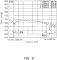
- FIG. 6 is a diagram of return loss of an antenna element in the notebook mode according to an embodiment of the invention
- FIG. 7 is a diagram of return loss of an antenna element in the tablet mode according to an embodiment of the invention.
- the antenna element 12 is operable in a first band 610 and a second band 620.
- the antenna element 12 keeps return loss in the first band 610 and the second band 620 under -10dB.
- the first portion in the first radiation portion of the invention faces the first edge of the ground plane and the second portion, and the second portion extends from the second edge of the ground plane.
- the space occupied by the first radiation portion in the Y-axis direction is reduced, so that the height of the antenna element in the Y-axis direction is reduced.
- the current-dividing path is used in the invention to adjust the impedance of the antenna element 12 operating in the second band, so as to reduce the space occupied by the second radiation portion in the Y-axis direction, so that the height of the antenna element in the Y-axis direction is further reduced.
- the antenna element in the communication device has the low-profile characteristic, so as to be feasible for narrow-frame designs.
Landscapes
- Engineering & Computer Science (AREA)
- Computer Networks & Wireless Communication (AREA)
- Signal Processing (AREA)
- Support Of Aerials (AREA)
- Waveguide Aerials (AREA)
- Details Of Aerials (AREA)
Claims (9)
- Kommunikationsvorrichtung (10), umfassend:eine Horizontalebene (11), die eine erste Kante (SD11) und eine benachbarte zweite Kante (SD12) umfasst;und ein Antennenelement (12), umfassend:einen nahe an der ersten Kante (SD11) der Horizontalebene (11) angeordneten Einspeiseabschnitt (120);einen ersten Strahlungsabschnitt (130), der mit dem Einspeiseabschnitt (120) einen ersten Resonanzpfad (210) bildet und einen ersten Abschnitt (131) und einen damit elektrisch verbundenen zweiten Abschnitt (132) aufweist,wobei der erste Abschnitt (131) der ersten Kante (SD 11) und dem zweiten Abschnitt (132) zugewandt ist und der zweite Abschnitt (132) sich von der zweiten Kante (SD12) weg erstreckt;einen zweiten Strahlungsabschnitt (140), der mit dem Einspeiseabschnitt (120) einen zweiten Resonanzpfad (310) bildet,wobei das Antennenelement (12) dafür ausgelegt ist, durch den ersten Resonanzpfad (210) und den zweiten Resonanzpfad (310) in einer ersten Bandbreite (610) und einer zweiten Bandbreite (620) zu arbeiten;und einen mit dem ersten Abschnitt (131) und dem zweiten Abschnitt (132) elektrisch verbundenen Einstellabschnitt (150), wobei der Einstellabschnitt (150) und ein Teil des ersten Strahlungsabschnitts (130) einen Stromteilerpfad (320) bilden, der dafür ausgelegt ist, die Impedanz des Antennenelements (12) in der zweiten Bandbreite (620) einzustellen,wobei der erste Abschnitt (131) je nach Platzierung des Einstellabschnitts (150) in ein erstes Segment (330) und ein zweites Segment (340) unterteilt ist,wobei das erste Segment (330) mit dem Einspeiseabschnitt (120) elektrisch verbunden ist, das zweite Segment (340) mit dem zweiten Abschnitt (132) elektrisch verbunden ist und das erste Segment (330) doppelt so lang ist wie das zweite Segment (340).
- Kommunikationsvorrichtung gemäß Anspruch 1,
wobei der Einspeiseabschnitt (120) ein erstes Ende des ersten Abschnitts (131) und ein erstes Ende des zweiten Strahlungsabschnitts (140) elektrisch verbindet, ein zweites Ende des zweiten Strahlungsabschnitts (140) ein offenes Ende aufweist, ein erstes Ende des zweiten Abschnitts (132) mit einem zweiten Ende des ersten Abschnitts (131) elektrisch verbunden ist und ein zweites Ende des zweiten Abschnitts (132) mit der zweiten Kante (SD12) elektrisch verbunden ist. - Kommunikationsvorrichtung gemäß Anspruch 1,
wobei der Einstellabschnitt (150) parallel zu einem Teil des zweiten Abschnitts (132) verläuft. - Kommunikationsvorrichtung gemäß Anspruch 3,
wobei der erste Abschnitt (131) linear geformt ist und der zweite Abschnitt (132) die Form eines umgekehrten L aufweist. - Kommunikationsvorrichtung gemäß Anspruch 4,
wobei der zweite Strahlungsabschnitt (140) die Form eines umgekehrten L aufweist. - Kommunikationsvorrichtung gemäß Anspruch 1,
wobei der erste Resonanzpfad (210) die halbe Wellenlänge der niedrigsten Frequenz der ersten Bandbreite (610) aufweist. - Kommunikationsvorrichtung gemäß Anspruch 1,
wobei der zweite Resonanzpfad (310) ein Viertel der Wellenlänge der niedrigsten Frequenz der zweiten Bandbreite (620) aufweist. - Kommunikationsvorrichtung gemäß Anspruch 1,
wobei der zweite Strahlungsabschnitt (140) eine Biegung aufweist, so dass ein Teil des zweiten Strahlungsabschnitts (140) parallel zum ersten Abschnitt (131) verläuft. - Kommunikationsvorrichtung gemäß Anspruch 1,
wobei der Stromteilerpfad (320) eine induktive Wirkung hat, um den kapazitiven Effekt zwischen dem zweiten Strahlungsabschnitt (140) und der Horizontalebene (11) zu reduzieren.
Applications Claiming Priority (1)
| Application Number | Priority Date | Filing Date | Title |
|---|---|---|---|
| TW104127828A TWI577087B (zh) | 2015-08-26 | 2015-08-26 | 通訊裝置 |
Publications (2)
| Publication Number | Publication Date |
|---|---|
| EP3136506A1 EP3136506A1 (de) | 2017-03-01 |
| EP3136506B1 true EP3136506B1 (de) | 2019-06-05 |
Family
ID=54771044
Family Applications (1)
| Application Number | Title | Priority Date | Filing Date |
|---|---|---|---|
| EP15197643.8A Not-in-force EP3136506B1 (de) | 2015-08-26 | 2015-12-02 | Kommunikationsvorrichtung |
Country Status (3)
| Country | Link |
|---|---|
| US (2) | US20170064052A1 (de) |
| EP (1) | EP3136506B1 (de) |
| TW (1) | TWI577087B (de) |
Families Citing this family (3)
| Publication number | Priority date | Publication date | Assignee | Title |
|---|---|---|---|---|
| TWI648908B (zh) * | 2017-05-09 | 2019-01-21 | 和碩聯合科技股份有限公司 | 電子裝置與其天線結構 |
| KR102245948B1 (ko) * | 2017-06-12 | 2021-04-30 | 삼성전자주식회사 | 안테나 및 안테나를 포함하는 전자 장치 |
| KR101958667B1 (ko) | 2017-09-08 | 2019-03-15 | 엘지전자 주식회사 | 이동 단말기 |
Citations (1)
| Publication number | Priority date | Publication date | Assignee | Title |
|---|---|---|---|---|
| US20130314297A1 (en) * | 2012-01-31 | 2013-11-28 | Panasonic Corporation | Antenna apparatus including two pairs of antennas provided respectively to be symmetric with respect to symmetric line |
Family Cites Families (14)
| Publication number | Priority date | Publication date | Assignee | Title |
|---|---|---|---|---|
| JP2001185938A (ja) * | 1999-12-27 | 2001-07-06 | Mitsubishi Electric Corp | 2周波共用アンテナ、多周波共用アンテナ、および2周波または多周波共用アレーアンテナ |
| US8290035B2 (en) * | 2007-07-11 | 2012-10-16 | Limberg Allen Leroy | Systems for reducing adverse effects of deep fades in DTV signals designed for mobile reception |
| TWM343257U (en) * | 2008-05-16 | 2008-10-21 | Cheng Uei Prec Ind Co Ltd | Dual-band antenna |
| WO2011024280A1 (ja) * | 2009-08-27 | 2011-03-03 | 株式会社 東芝 | アンテナ装置及び通信装置 |
| TWM398213U (en) * | 2010-07-02 | 2011-02-11 | Wistron Neweb Corp | Wideband antenna |
| JP5060629B1 (ja) * | 2011-03-30 | 2012-10-31 | 株式会社東芝 | アンテナ装置とこのアンテナ装置を備えた電子機器 |
| WO2013016575A2 (en) * | 2011-07-28 | 2013-01-31 | Skyworks Solutions, Inc. | Low variation current multiplier |
| JP5127966B1 (ja) * | 2011-08-30 | 2013-01-23 | 株式会社東芝 | アンテナ装置とこのアンテナ装置を備えた電子機器 |
| US8933385B2 (en) * | 2012-07-06 | 2015-01-13 | Omnivision Technologies, Inc. | Hybrid analog-to-digital converter having multiple ADC modes |
| TWI532253B (zh) * | 2012-09-10 | 2016-05-01 | 鴻海精密工業股份有限公司 | 多頻天線 |
| TWI508367B (zh) * | 2012-09-27 | 2015-11-11 | Ind Tech Res Inst | 通訊裝置及其天線元件之設計方法 |
| TW201526389A (zh) * | 2013-12-31 | 2015-07-01 | Acer Inc | 無線通訊裝置 |
| TWI538310B (zh) * | 2014-01-08 | 2016-06-11 | 智易科技股份有限公司 | 雙頻印刷式的單極天線 |
| US9419346B2 (en) * | 2014-01-15 | 2016-08-16 | Broadcom Corporation | High isolation antenna structure on a ground plane |
-
2015
- 2015-08-26 TW TW104127828A patent/TWI577087B/zh not_active IP Right Cessation
- 2015-11-25 US US14/951,511 patent/US20170064052A1/en not_active Abandoned
- 2015-12-02 EP EP15197643.8A patent/EP3136506B1/de not_active Not-in-force
-
2018
- 2018-04-11 US US15/951,148 patent/US20180234528A1/en not_active Abandoned
Patent Citations (1)
| Publication number | Priority date | Publication date | Assignee | Title |
|---|---|---|---|---|
| US20130314297A1 (en) * | 2012-01-31 | 2013-11-28 | Panasonic Corporation | Antenna apparatus including two pairs of antennas provided respectively to be symmetric with respect to symmetric line |
Also Published As
| Publication number | Publication date |
|---|---|
| US20180234528A1 (en) | 2018-08-16 |
| EP3136506A1 (de) | 2017-03-01 |
| US20170064052A1 (en) | 2017-03-02 |
| TW201709609A (zh) | 2017-03-01 |
| TWI577087B (zh) | 2017-04-01 |
Similar Documents
| Publication | Publication Date | Title |
|---|---|---|
| US10446915B2 (en) | Mobile device | |
| US10910698B2 (en) | Mobile device and antenna structure | |
| US11038258B2 (en) | Mobile device and antenna structure | |
| US10056696B2 (en) | Antenna structure | |
| TWI655803B (zh) | 行動裝置及其製造方法 | |
| US8948827B2 (en) | Mobile communication device | |
| JP5382477B2 (ja) | スロットアンテナ | |
| US10096889B2 (en) | Mobile device | |
| US7265720B1 (en) | Planar inverted-F antenna with parasitic conductor loop and device using same | |
| US10069196B1 (en) | Mobile device | |
| US20170104261A1 (en) | Communication device | |
| US20110102272A1 (en) | Mobile Communication Device and Antenna Thereof | |
| US10135141B2 (en) | Mobile device | |
| CN103682587A (zh) | 移动装置 | |
| US9343801B2 (en) | Electronic device | |
| EP3220478B1 (de) | Diversitätsantenne | |
| JP6015944B2 (ja) | アンテナ装置、通信装置、及び電子機器 | |
| US10910696B2 (en) | Mobile device | |
| US9048532B2 (en) | Multi-band antenna | |
| EP3136506B1 (de) | Kommunikationsvorrichtung | |
| US10811775B2 (en) | Loop antenna | |
| US9124001B2 (en) | Communication device and antenna element therein | |
| US20150214618A1 (en) | Communication device and antenna element therein | |
| US11322826B2 (en) | Antenna structure | |
| US10826178B2 (en) | Multi-band antenna |
Legal Events
| Date | Code | Title | Description |
|---|---|---|---|
| PUAI | Public reference made under article 153(3) epc to a published international application that has entered the european phase |
Free format text: ORIGINAL CODE: 0009012 |
|
| STAA | Information on the status of an ep patent application or granted ep patent |
Free format text: STATUS: THE APPLICATION HAS BEEN PUBLISHED |
|
| AK | Designated contracting states |
Kind code of ref document: A1 Designated state(s): AL AT BE BG CH CY CZ DE DK EE ES FI FR GB GR HR HU IE IS IT LI LT LU LV MC MK MT NL NO PL PT RO RS SE SI SK SM TR |
|
| AX | Request for extension of the european patent |
Extension state: BA ME |
|
| STAA | Information on the status of an ep patent application or granted ep patent |
Free format text: STATUS: REQUEST FOR EXAMINATION WAS MADE |
|
| 17P | Request for examination filed |
Effective date: 20170814 |
|
| RBV | Designated contracting states (corrected) |
Designated state(s): AL AT BE BG CH CY CZ DE DK EE ES FI FR GB GR HR HU IE IS IT LI LT LU LV MC MK MT NL NO PL PT RO RS SE SI SK SM TR |
|
| STAA | Information on the status of an ep patent application or granted ep patent |
Free format text: STATUS: EXAMINATION IS IN PROGRESS |
|
| 17Q | First examination report despatched |
Effective date: 20171207 |
|
| GRAP | Despatch of communication of intention to grant a patent |
Free format text: ORIGINAL CODE: EPIDOSNIGR1 |
|
| STAA | Information on the status of an ep patent application or granted ep patent |
Free format text: STATUS: GRANT OF PATENT IS INTENDED |
|
| RIC1 | Information provided on ipc code assigned before grant |
Ipc: H01Q 9/42 20060101ALI20190117BHEP Ipc: H01Q 7/00 20060101ALN20190117BHEP Ipc: H01Q 1/24 20060101ALI20190117BHEP Ipc: H01Q 5/364 20150101AFI20190117BHEP Ipc: H01Q 1/38 20060101ALI20190117BHEP |
|
| INTG | Intention to grant announced |
Effective date: 20190201 |
|
| GRAS | Grant fee paid |
Free format text: ORIGINAL CODE: EPIDOSNIGR3 |
|
| GRAA | (expected) grant |
Free format text: ORIGINAL CODE: 0009210 |
|
| STAA | Information on the status of an ep patent application or granted ep patent |
Free format text: STATUS: THE PATENT HAS BEEN GRANTED |
|
| AK | Designated contracting states |
Kind code of ref document: B1 Designated state(s): AL AT BE BG CH CY CZ DE DK EE ES FI FR GB GR HR HU IE IS IT LI LT LU LV MC MK MT NL NO PL PT RO RS SE SI SK SM TR |
|
| REG | Reference to a national code |
Ref country code: GB Ref legal event code: FG4D |
|
| REG | Reference to a national code |
Ref country code: CH Ref legal event code: EP |
|
| REG | Reference to a national code |
Ref country code: AT Ref legal event code: REF Ref document number: 1140939 Country of ref document: AT Kind code of ref document: T Effective date: 20190615 |
|
| REG | Reference to a national code |
Ref country code: IE Ref legal event code: FG4D |
|
| REG | Reference to a national code |
Ref country code: DE Ref legal event code: R096 Ref document number: 602015031315 Country of ref document: DE |
|
| REG | Reference to a national code |
Ref country code: NL Ref legal event code: MP Effective date: 20190605 |
|
| REG | Reference to a national code |
Ref country code: LT Ref legal event code: MG4D |
|
| PG25 | Lapsed in a contracting state [announced via postgrant information from national office to epo] |
Ref country code: AL Free format text: LAPSE BECAUSE OF FAILURE TO SUBMIT A TRANSLATION OF THE DESCRIPTION OR TO PAY THE FEE WITHIN THE PRESCRIBED TIME-LIMIT Effective date: 20190605 Ref country code: SE Free format text: LAPSE BECAUSE OF FAILURE TO SUBMIT A TRANSLATION OF THE DESCRIPTION OR TO PAY THE FEE WITHIN THE PRESCRIBED TIME-LIMIT Effective date: 20190605 Ref country code: FI Free format text: LAPSE BECAUSE OF FAILURE TO SUBMIT A TRANSLATION OF THE DESCRIPTION OR TO PAY THE FEE WITHIN THE PRESCRIBED TIME-LIMIT Effective date: 20190605 Ref country code: NO Free format text: LAPSE BECAUSE OF FAILURE TO SUBMIT A TRANSLATION OF THE DESCRIPTION OR TO PAY THE FEE WITHIN THE PRESCRIBED TIME-LIMIT Effective date: 20190905 Ref country code: HR Free format text: LAPSE BECAUSE OF FAILURE TO SUBMIT A TRANSLATION OF THE DESCRIPTION OR TO PAY THE FEE WITHIN THE PRESCRIBED TIME-LIMIT Effective date: 20190605 Ref country code: ES Free format text: LAPSE BECAUSE OF FAILURE TO SUBMIT A TRANSLATION OF THE DESCRIPTION OR TO PAY THE FEE WITHIN THE PRESCRIBED TIME-LIMIT Effective date: 20190605 Ref country code: LT Free format text: LAPSE BECAUSE OF FAILURE TO SUBMIT A TRANSLATION OF THE DESCRIPTION OR TO PAY THE FEE WITHIN THE PRESCRIBED TIME-LIMIT Effective date: 20190605 |
|
| PG25 | Lapsed in a contracting state [announced via postgrant information from national office to epo] |
Ref country code: LV Free format text: LAPSE BECAUSE OF FAILURE TO SUBMIT A TRANSLATION OF THE DESCRIPTION OR TO PAY THE FEE WITHIN THE PRESCRIBED TIME-LIMIT Effective date: 20190605 Ref country code: RS Free format text: LAPSE BECAUSE OF FAILURE TO SUBMIT A TRANSLATION OF THE DESCRIPTION OR TO PAY THE FEE WITHIN THE PRESCRIBED TIME-LIMIT Effective date: 20190605 Ref country code: BG Free format text: LAPSE BECAUSE OF FAILURE TO SUBMIT A TRANSLATION OF THE DESCRIPTION OR TO PAY THE FEE WITHIN THE PRESCRIBED TIME-LIMIT Effective date: 20190905 Ref country code: GR Free format text: LAPSE BECAUSE OF FAILURE TO SUBMIT A TRANSLATION OF THE DESCRIPTION OR TO PAY THE FEE WITHIN THE PRESCRIBED TIME-LIMIT Effective date: 20190906 |
|
| REG | Reference to a national code |
Ref country code: AT Ref legal event code: MK05 Ref document number: 1140939 Country of ref document: AT Kind code of ref document: T Effective date: 20190605 |
|
| PG25 | Lapsed in a contracting state [announced via postgrant information from national office to epo] |
Ref country code: CZ Free format text: LAPSE BECAUSE OF FAILURE TO SUBMIT A TRANSLATION OF THE DESCRIPTION OR TO PAY THE FEE WITHIN THE PRESCRIBED TIME-LIMIT Effective date: 20190605 Ref country code: AT Free format text: LAPSE BECAUSE OF FAILURE TO SUBMIT A TRANSLATION OF THE DESCRIPTION OR TO PAY THE FEE WITHIN THE PRESCRIBED TIME-LIMIT Effective date: 20190605 Ref country code: EE Free format text: LAPSE BECAUSE OF FAILURE TO SUBMIT A TRANSLATION OF THE DESCRIPTION OR TO PAY THE FEE WITHIN THE PRESCRIBED TIME-LIMIT Effective date: 20190605 Ref country code: SK Free format text: LAPSE BECAUSE OF FAILURE TO SUBMIT A TRANSLATION OF THE DESCRIPTION OR TO PAY THE FEE WITHIN THE PRESCRIBED TIME-LIMIT Effective date: 20190605 Ref country code: RO Free format text: LAPSE BECAUSE OF FAILURE TO SUBMIT A TRANSLATION OF THE DESCRIPTION OR TO PAY THE FEE WITHIN THE PRESCRIBED TIME-LIMIT Effective date: 20190605 Ref country code: NL Free format text: LAPSE BECAUSE OF FAILURE TO SUBMIT A TRANSLATION OF THE DESCRIPTION OR TO PAY THE FEE WITHIN THE PRESCRIBED TIME-LIMIT Effective date: 20190605 Ref country code: PT Free format text: LAPSE BECAUSE OF FAILURE TO SUBMIT A TRANSLATION OF THE DESCRIPTION OR TO PAY THE FEE WITHIN THE PRESCRIBED TIME-LIMIT Effective date: 20191007 |
|
| PG25 | Lapsed in a contracting state [announced via postgrant information from national office to epo] |
Ref country code: IT Free format text: LAPSE BECAUSE OF FAILURE TO SUBMIT A TRANSLATION OF THE DESCRIPTION OR TO PAY THE FEE WITHIN THE PRESCRIBED TIME-LIMIT Effective date: 20190605 Ref country code: SM Free format text: LAPSE BECAUSE OF FAILURE TO SUBMIT A TRANSLATION OF THE DESCRIPTION OR TO PAY THE FEE WITHIN THE PRESCRIBED TIME-LIMIT Effective date: 20190605 Ref country code: IS Free format text: LAPSE BECAUSE OF FAILURE TO SUBMIT A TRANSLATION OF THE DESCRIPTION OR TO PAY THE FEE WITHIN THE PRESCRIBED TIME-LIMIT Effective date: 20191005 |
|
| REG | Reference to a national code |
Ref country code: DE Ref legal event code: R097 Ref document number: 602015031315 Country of ref document: DE |
|
| PG25 | Lapsed in a contracting state [announced via postgrant information from national office to epo] |
Ref country code: TR Free format text: LAPSE BECAUSE OF FAILURE TO SUBMIT A TRANSLATION OF THE DESCRIPTION OR TO PAY THE FEE WITHIN THE PRESCRIBED TIME-LIMIT Effective date: 20190605 |
|
| PLBE | No opposition filed within time limit |
Free format text: ORIGINAL CODE: 0009261 |
|
| STAA | Information on the status of an ep patent application or granted ep patent |
Free format text: STATUS: NO OPPOSITION FILED WITHIN TIME LIMIT |
|
| PG25 | Lapsed in a contracting state [announced via postgrant information from national office to epo] |
Ref country code: PL Free format text: LAPSE BECAUSE OF FAILURE TO SUBMIT A TRANSLATION OF THE DESCRIPTION OR TO PAY THE FEE WITHIN THE PRESCRIBED TIME-LIMIT Effective date: 20190605 Ref country code: DK Free format text: LAPSE BECAUSE OF FAILURE TO SUBMIT A TRANSLATION OF THE DESCRIPTION OR TO PAY THE FEE WITHIN THE PRESCRIBED TIME-LIMIT Effective date: 20190605 |
|
| 26N | No opposition filed |
Effective date: 20200306 |
|
| PG25 | Lapsed in a contracting state [announced via postgrant information from national office to epo] |
Ref country code: SI Free format text: LAPSE BECAUSE OF FAILURE TO SUBMIT A TRANSLATION OF THE DESCRIPTION OR TO PAY THE FEE WITHIN THE PRESCRIBED TIME-LIMIT Effective date: 20190605 |
|
| REG | Reference to a national code |
Ref country code: CH Ref legal event code: PL |
|
| REG | Reference to a national code |
Ref country code: BE Ref legal event code: MM Effective date: 20191231 |
|
| PG25 | Lapsed in a contracting state [announced via postgrant information from national office to epo] |
Ref country code: MC Free format text: LAPSE BECAUSE OF FAILURE TO SUBMIT A TRANSLATION OF THE DESCRIPTION OR TO PAY THE FEE WITHIN THE PRESCRIBED TIME-LIMIT Effective date: 20190605 |
|
| PG25 | Lapsed in a contracting state [announced via postgrant information from national office to epo] |
Ref country code: LU Free format text: LAPSE BECAUSE OF NON-PAYMENT OF DUE FEES Effective date: 20191202 Ref country code: IE Free format text: LAPSE BECAUSE OF NON-PAYMENT OF DUE FEES Effective date: 20191202 |
|
| PG25 | Lapsed in a contracting state [announced via postgrant information from national office to epo] |
Ref country code: BE Free format text: LAPSE BECAUSE OF NON-PAYMENT OF DUE FEES Effective date: 20191231 Ref country code: CH Free format text: LAPSE BECAUSE OF NON-PAYMENT OF DUE FEES Effective date: 20191231 Ref country code: LI Free format text: LAPSE BECAUSE OF NON-PAYMENT OF DUE FEES Effective date: 20191231 |
|
| PG25 | Lapsed in a contracting state [announced via postgrant information from national office to epo] |
Ref country code: CY Free format text: LAPSE BECAUSE OF FAILURE TO SUBMIT A TRANSLATION OF THE DESCRIPTION OR TO PAY THE FEE WITHIN THE PRESCRIBED TIME-LIMIT Effective date: 20190605 |
|
| PG25 | Lapsed in a contracting state [announced via postgrant information from national office to epo] |
Ref country code: MT Free format text: LAPSE BECAUSE OF FAILURE TO SUBMIT A TRANSLATION OF THE DESCRIPTION OR TO PAY THE FEE WITHIN THE PRESCRIBED TIME-LIMIT Effective date: 20190605 Ref country code: HU Free format text: LAPSE BECAUSE OF FAILURE TO SUBMIT A TRANSLATION OF THE DESCRIPTION OR TO PAY THE FEE WITHIN THE PRESCRIBED TIME-LIMIT; INVALID AB INITIO Effective date: 20151202 |
|
| PG25 | Lapsed in a contracting state [announced via postgrant information from national office to epo] |
Ref country code: MK Free format text: LAPSE BECAUSE OF FAILURE TO SUBMIT A TRANSLATION OF THE DESCRIPTION OR TO PAY THE FEE WITHIN THE PRESCRIBED TIME-LIMIT Effective date: 20190605 |
|
| PGFP | Annual fee paid to national office [announced via postgrant information from national office to epo] |
Ref country code: GB Payment date: 20231109 Year of fee payment: 9 |
|
| PGFP | Annual fee paid to national office [announced via postgrant information from national office to epo] |
Ref country code: FR Payment date: 20231108 Year of fee payment: 9 Ref country code: DE Payment date: 20231107 Year of fee payment: 9 |
|
| REG | Reference to a national code |
Ref country code: DE Ref legal event code: R119 Ref document number: 602015031315 Country of ref document: DE |
|
| GBPC | Gb: european patent ceased through non-payment of renewal fee |
Effective date: 20241202 |
|
| PG25 | Lapsed in a contracting state [announced via postgrant information from national office to epo] |
Ref country code: DE Free format text: LAPSE BECAUSE OF NON-PAYMENT OF DUE FEES Effective date: 20250701 |
|
| PG25 | Lapsed in a contracting state [announced via postgrant information from national office to epo] |
Ref country code: GB Free format text: LAPSE BECAUSE OF NON-PAYMENT OF DUE FEES Effective date: 20241202 |
|
| PG25 | Lapsed in a contracting state [announced via postgrant information from national office to epo] |
Ref country code: FR Free format text: LAPSE BECAUSE OF NON-PAYMENT OF DUE FEES Effective date: 20241231 |