EP3134712B1 - Bestimmung der dicke und zusammensetzung von silicium-germanium mit kombinierter xps- und xrf-technologie - Google Patents
Bestimmung der dicke und zusammensetzung von silicium-germanium mit kombinierter xps- und xrf-technologie Download PDFInfo
- Publication number
- EP3134712B1 EP3134712B1 EP15782815.3A EP15782815A EP3134712B1 EP 3134712 B1 EP3134712 B1 EP 3134712B1 EP 15782815 A EP15782815 A EP 15782815A EP 3134712 B1 EP3134712 B1 EP 3134712B1
- Authority
- EP
- European Patent Office
- Prior art keywords
- signal
- xps
- xrf
- silicon germanium
- ray
- Prior art date
- Legal status (The legal status is an assumption and is not a legal conclusion. Google has not performed a legal analysis and makes no representation as to the accuracy of the status listed.)
- Active
Links
Images







Classifications
-
- G—PHYSICS
- G01—MEASURING; TESTING
- G01N—INVESTIGATING OR ANALYSING MATERIALS BY DETERMINING THEIR CHEMICAL OR PHYSICAL PROPERTIES
- G01N23/00—Investigating or analysing materials by the use of wave or particle radiation, e.g. X-rays or neutrons, not covered by groups G01N3/00 – G01N17/00, G01N21/00 or G01N22/00
- G01N23/22—Investigating or analysing materials by the use of wave or particle radiation, e.g. X-rays or neutrons, not covered by groups G01N3/00 – G01N17/00, G01N21/00 or G01N22/00 by measuring secondary emission from the material
- G01N23/2206—Combination of two or more measurements, at least one measurement being that of secondary emission, e.g. combination of secondary electron [SE] measurement and back-scattered electron [BSE] measurement
-
- G—PHYSICS
- G01—MEASURING; TESTING
- G01B—MEASURING LENGTH, THICKNESS OR SIMILAR LINEAR DIMENSIONS; MEASURING ANGLES; MEASURING AREAS; MEASURING IRREGULARITIES OF SURFACES OR CONTOURS
- G01B15/00—Measuring arrangements characterised by the use of electromagnetic waves or particle radiation, e.g. by the use of microwaves, X-rays, gamma rays or electrons
- G01B15/02—Measuring arrangements characterised by the use of electromagnetic waves or particle radiation, e.g. by the use of microwaves, X-rays, gamma rays or electrons for measuring thickness
-
- G—PHYSICS
- G01—MEASURING; TESTING
- G01N—INVESTIGATING OR ANALYSING MATERIALS BY DETERMINING THEIR CHEMICAL OR PHYSICAL PROPERTIES
- G01N15/00—Investigating characteristics of particles; Investigating permeability, pore-volume or surface-area of porous materials
- G01N15/02—Investigating particle size or size distribution
-
- G—PHYSICS
- G01—MEASURING; TESTING
- G01N—INVESTIGATING OR ANALYSING MATERIALS BY DETERMINING THEIR CHEMICAL OR PHYSICAL PROPERTIES
- G01N23/00—Investigating or analysing materials by the use of wave or particle radiation, e.g. X-rays or neutrons, not covered by groups G01N3/00 – G01N17/00, G01N21/00 or G01N22/00
- G01N23/22—Investigating or analysing materials by the use of wave or particle radiation, e.g. X-rays or neutrons, not covered by groups G01N3/00 – G01N17/00, G01N21/00 or G01N22/00 by measuring secondary emission from the material
- G01N23/2206—Combination of two or more measurements, at least one measurement being that of secondary emission, e.g. combination of secondary electron [SE] measurement and back-scattered electron [BSE] measurement
- G01N23/2208—Combination of two or more measurements, at least one measurement being that of secondary emission, e.g. combination of secondary electron [SE] measurement and back-scattered electron [BSE] measurement all measurements being of a secondary emission, e.g. combination of SE measurement and characteristic X-ray measurement
-
- G—PHYSICS
- G01—MEASURING; TESTING
- G01N—INVESTIGATING OR ANALYSING MATERIALS BY DETERMINING THEIR CHEMICAL OR PHYSICAL PROPERTIES
- G01N23/00—Investigating or analysing materials by the use of wave or particle radiation, e.g. X-rays or neutrons, not covered by groups G01N3/00 – G01N17/00, G01N21/00 or G01N22/00
- G01N23/22—Investigating or analysing materials by the use of wave or particle radiation, e.g. X-rays or neutrons, not covered by groups G01N3/00 – G01N17/00, G01N21/00 or G01N22/00 by measuring secondary emission from the material
- G01N23/223—Investigating or analysing materials by the use of wave or particle radiation, e.g. X-rays or neutrons, not covered by groups G01N3/00 – G01N17/00, G01N21/00 or G01N22/00 by measuring secondary emission from the material by irradiating the sample with X-rays or gamma-rays and by measuring X-ray fluorescence
-
- G—PHYSICS
- G01—MEASURING; TESTING
- G01N—INVESTIGATING OR ANALYSING MATERIALS BY DETERMINING THEIR CHEMICAL OR PHYSICAL PROPERTIES
- G01N23/00—Investigating or analysing materials by the use of wave or particle radiation, e.g. X-rays or neutrons, not covered by groups G01N3/00 – G01N17/00, G01N21/00 or G01N22/00
- G01N23/22—Investigating or analysing materials by the use of wave or particle radiation, e.g. X-rays or neutrons, not covered by groups G01N3/00 – G01N17/00, G01N21/00 or G01N22/00 by measuring secondary emission from the material
- G01N23/227—Measuring photoelectric effect, e.g. photoelectron emission microscopy [PEEM]
- G01N23/2273—Measuring photoelectron spectrum, e.g. electron spectroscopy for chemical analysis [ESCA] or X-ray photoelectron spectroscopy [XPS]
-
- G—PHYSICS
- G01—MEASURING; TESTING
- G01N—INVESTIGATING OR ANALYSING MATERIALS BY DETERMINING THEIR CHEMICAL OR PHYSICAL PROPERTIES
- G01N2223/00—Investigating materials by wave or particle radiation
- G01N2223/60—Specific applications or type of materials
- G01N2223/61—Specific applications or type of materials thin films, coatings
-
- G—PHYSICS
- G01—MEASURING; TESTING
- G01N—INVESTIGATING OR ANALYSING MATERIALS BY DETERMINING THEIR CHEMICAL OR PHYSICAL PROPERTIES
- G01N2223/00—Investigating materials by wave or particle radiation
- G01N2223/60—Specific applications or type of materials
- G01N2223/611—Specific applications or type of materials patterned objects; electronic devices
- G01N2223/6116—Specific applications or type of materials patterned objects; electronic devices semiconductor wafer
Definitions
- Embodiments of the invention are in the field of combined XPS and XRF technologies and, in particular, silicon germanium thickness and composition determination using combined XPS and XRF technologies.
- X-ray photoelectron spectroscopy is a quantitative spectroscopic technique that measures the elemental composition, empirical formula, chemical state and electronic state of the elements that exist within a material.
- XPS spectra may be obtained by irradiating a material with a beam of X-rays while simultaneously measuring the kinetic energy and number of electrons that escape from the top, e.g., 1 to 10 nm of the material being analyzed.
- XPS analysis commonly employs monochromatic aluminum K ⁇ (AlK ⁇ ) X-rays, which may be generated by bombarding an aluminum anode surface with a focused electron beam.
- a fraction of the generated AlK ⁇ X-rays is then intercepted by a focusing monochromator and a narrow X-ray energy band is focused onto the analysis site on a sample surface.
- the X-ray flux of the AlK ⁇ X-rays at the sample surface depends on the electron beam current, the thickness and integrity of the aluminum anode surface, and crystal quality, size, and stability of the monochromator.
- X-ray fluorescence is the emission of characteristic "secondary" (or fluorescent) X-rays from a material that has been excited by bombarding with higher energy X- rays or gamma rays.
- the phenomenon is widely used for elemental analysis and chemical analysis, particularly in the investigation of metals, glass, ceramics and building materials, and for research in geochemistry, forensic science and archaeology.
- XPS analysis and XRF analysis each have their own advantages as techniques for sample characterization. Thus, advances are needed in analyses based on XPS and/or XRF detection.
- a system for characterizing a film may include an X-ray source for generating an X-ray beam having an energy below the k-edge of silicon.
- a sample holder may be included for positioning a sample in a pathway of the X-ray beam.
- a first detector may be included for collecting an XPS signal generated by bombarding the sample with the X-ray beam.
- a second detector may be included for collecting an X-ray fluorescence (XRF) signal generated by bombarding the sample with the X-ray beam.
- XRF X-ray fluorescence
- Monitoring/estimation of the primary X-ray flux at the analysis site may be provided by X-ray flux detectors near and at the analysis site. Both XRF and XPS signals may be normalized to the (estimated) primary X-ray flux to enable film thickness or dose measurement without the need to employ signal intensity ratios.
- Document US 7 358 494 B1 discloses that the material composition of a thin film formed on a substrate or covered by a cap layer that shares one or more elements with the thin film can be determined by combining characteristic material data, such as characteristic x-ray data, from a material composition analysis tool, such as an electron probe-based x-ray metrology (EPMA) operation, with thickness data and (optionally) possible material phases for the thin film.
- characteristic material data such as characteristic x-ray data
- a material composition analysis tool such as an electron probe-based x-ray metrology (EPMA) operation
- the thickness data and/or the material phase options can be used to determine, for example, the penetration depth of a probe e-beam of the EPMA tool.
- the characteristic x-ray data from the EPMA operation can be analyzed to determine the composition (e.g., phase or elemental composition) of the thin film.
- An EPMA tool can include ellipsometry capabilities for all-in-one thickness and composition determination.
- Document WO 2013/035082 A1 discloses a combined method of secondary ion mass spectroscopy and energy dispersed X-ray for quantitative chemical analysis of solid materials and thin films, comprising the steps of a) installing an energy dispersed detector on a free port of a mass spectrometer for X-ray recording, b) placing the study sample in an ultrahigh vacuum chamber of the mass spectrometer, c) activating the electron gun for the mass spectrometer to achieve the characteristic X-ray excitation of the study sample, wherein the electron gun provides a moderately focused electron beam with energies that can vary from 0 to 15keV and currents from 0 to 100 mA, d) analyzing the X-rays generated in step c) with the energy dispersed detector, and find sensibility factors, e) calibrating the ion mass spectroscopy data with the sensitivity factors obtained by energy dispersed X-ray quantitative analysis of step d) using existing theories and f) analyzing with ion mass spect
- Ellipsometry can be used in situ and is a much more sensitive method, but this technique needs more research to correlate the nucleation process with the data obtained using this technique.
- the determination of the nucleus density using scanning electron microscopy or atomic force microscope is the most accurate method, yet needs a lot of experiments. Without a detailed description of the measurement method the incubation time is a meaningless quantity.
- an optical thin film is formed of particles consisting principally of silver which has a specified particle size, an inter-particle distance, and particle number density an element selected out of titanium, zirconium, vanadium, niobium, tantalum, chrome, molybdenum, tungsten, manganese, silicon, germanium, phosphorus, and oxygen to provide an optical thin film which varies its transmissivity reversibly by ultraviolet ray irradiation and visible ray irradiation, is large in variation width and has a high transmissivity and a low haze, and to provide an optical thin film which can be manufactured through a simple process.
- Document US 2006/062350 A1 discloses an apparatus for analysis of a sample includes a radiation source, which is adapted to direct a converging beam of X-rays toward a surface of the sample. At least one detector array is arranged to sense the X-rays scattered from the sample as a function of elevation angle over a range of elevation angles simultaneously, and to generate output signals responsively to the scattered X-rays.
- the detector array has a first configuration in which the detector array senses the X-rays that are reflected from the surface of the sample at a grazing angle, and a second configuration in which the detector array senses the X-rays that are diffracted from the surface in a vicinity of a Bragg angle of the sample.
- a signal processor processes the output signals so as to determine a characteristic of the surface layer of the sample.
- One or more embodiments are directed to silicon germanium thickness and composition determination using combined XPS and XRF technologies.
- a method for characterizing a silicon germanium film includes generating an X-ray beam.
- a sample is positioned in a pathway of said X-ray beam.
- An X-ray photoelectron spectroscopy (XPS) signal generated by bombarding said sample with said X-ray beam is collected.
- An X-ray fluorescence (XRF) signal generated by bombarding said sample with said X-ray beam is also collected.
- a composition of the silicon germanium film from the XRF signal and the XPS signal is determined, characterized by determining the composition of thin silicon germanium film on Si-containing substrate, using comparing the XRF signal and the XPS signal to a realistic material layer mixing model that scales the predicted intensity of an XPS Ge signal and an XRF Ge signal relative to a pure germanium film, constraining the remaining fraction of the silicon germanium film to Si.
- a method for characterizing a silicon germanium film includes generating an X-ray beam.
- a sample is positioned in a pathway of said X-ray beam.
- An X-ray photoelectron spectroscopy (XPS) signal generated by bombarding said sample with said X-ray beam is collected.
- An X-ray fluorescence (XRF) signal generated by bombarding said sample with said X-ray beam is also collected.
- a composition of the silicon germanium film from the XRF signal and the XPS signal is determined, characterized by determining the composition of thin silicon germanium film on Si-containing substrate, using comparing the XRF signal and the XPS signal to a realistic material layer mixing model that scales the predicted intensity of an XPS Ge signal and an XRF Ge signal relative to a pure germanium film, constraining the remaining fraction of the silicon germanium film to Si.
- a thickness of the silicon germanium film is determined from the XRF signal and the XPS signal.
- a system for characterizing a silicon germanium film includes an X-ray source for generating an X-ray beam.
- the system also includes a sample holder for positioning a sample in a pathway of said X-ray beam.
- the system also includes a first detector for collecting an X-ray photoelectron spectroscopy (XPS) signal generated by bombarding said sample with said X-ray beam.
- the system also includes a second detector for collecting an X-ray fluorescence (XRF) signal generated by bombarding said sample with said X- ray beam.
- XPS X-ray photoelectron spectroscopy
- XRF X-ray fluorescence
- the XRF signal and the XPS signal are for determining a thickness or a composition, or both, of the silicon germanium film, characterized by determining the composition of thin silicon germanium film on Si-containing substrate using comparing the XRF signal and the XPS signal to a realistic material layer mixing model that scales the predicted intensity of an XPS Ge signal and an XRF Ge signal relative to a pure germanium film, constraining the remaining fraction of the silicon germanium film to Si.
- One or more embodiments are directed to the detection and use of photo-electron and X-ray fluorescent signals from the silicon (Si) and germanium (Ge) atoms in a silicon germanium (SiGe) thin film in combination with a realistic material mixing model to allow for the unique, unambiguous and stable determination of the SiGe thickness and the Ge% atomic composition applicable to realistic fab production needs.
- Si silicon
- germanium germanium
- Embodiments of the present invention address the problem of simultaneous determination and process control of Silicon Germanium thickness and Ge% atomic composition.
- Technical advantages of embodiments of the present invention include providing new capability for accurate, repeatable determination of thin SiGe thickness and Ge composition in a fab environment for production use.
- one or more embodiments of the present invention employ the combination of XPS and XRF signals along with a realistic film stack model to simultaneously determine a thin film SiGe thickness and compositional film properties.
- New film-stack algorithms can be employed to most accurately and robustly determine the SiGe thickness and Ge composition (%) over significant ranges using both the XPS (Si, Ge3d) and XRF (GeL ⁇ ) measured intensities.
- a generic film stack model that accounts for the generation of a Si XPS signal from both the SiGe film and crystalline silicon substrate (if appropriate) is used, along with (ii) a realistic material layer mixing model that scales the predicted intensity of the XPS and XRF Ge signals relative to an otherwise pure Ge film, constraining the remaining fraction of the film to Si.
- SiGe technology has played an increasing role in p-type field effect transistor (pFET) performance boost and threshold voltage (V t ) tunability.
- pFET p-type field effect transistor
- V t threshold voltage
- SiGe embedded (e-SiGe) in the source-drain region produces uniaxial strain in p-type metal oxide semiconductor (PMOS) channels.
- PMOS p-type metal oxide semiconductor
- SiGe is being considered as a replacement for the conventional Si channel to achieve higher hole mobility.
- thickness and composition of SiGe, especially channel SiGe (cSiGe) has become one of the critical control parameters for semiconductor device performance. Capability of in-line metrology directly on product wafers is highly desirable in high- volume manufacturing.
- X-ray diffraction is another commonly used technique for SiGe film measurements.
- XRD X-ray diffraction
- measurements of both composition and thickness of a thin SiGe film on various substrates such as bulk-Si, silicon-on-insulator (SOI), and ultra-thin SOI, are achieved with simultaneous XPS and XRF measurements.
- XPS has recently proven to be an effective metrology for ultrathin films (e.g., less than approximately 100 Angstroms in thickness), with good sensitivity to both composition and thickness.
- ultrathin films e.g., less than approximately 100 Angstroms in thickness
- HKMG high-k metal gate
- FinFET Fin field effect transistor
- XPS cannot differentiate between the Si signal from the SiGe film and the signal from the Si substrate. With only one independent signal which is the Ge XPS signal, XPS alone cannot independently determine both variables, which are the composition and thickness.
- this problem is resolved by taking advantage of the GeL ⁇ XRF signal that is also generated at the same time during the XPS measurement.
- the XRF signal provides an additional independent signal that, when combined with the XPS signals, allows for the measurement of both thickness and composition.
- both XPS and XRF information may be obtained from a single metrology tool.
- Figure 1 illustrates an angled view of an XPS and XRF combination tool 100, in accordance with an embodiment of the present invention. Measurements described herein were performed on an in-line XPS and XRF combination tool such as combination tool 100.
- the XPS and XRF combination tool 100 is capable of measuring 300mm wafers within a 50 ⁇ m 2 metrology box.
- the XPS and XRF combination tool 100 is operated while maintained under a base pressure of less than approximately 1.33E -7 mbar (1.0E-7 Torr).
- a base pressure of less than approximately 1.33E -7 mbar (1.0E-7 Torr).
- x-ray 104 is generated from an aluminum anode 106 at 1486.7eV.
- a monochromatic AlK ⁇ x-ray 108 is then focused on to a wafer 110 by a high quality quartz crystal monochromator 112.
- a magnetic lens 114 under the wafer 110 generates magnetic field near the wafer 110 surface and focuses the photoelectrons 116 generated into an XPS spectrometer including XPS input optics 118, an XPS energy analyzer 120 (e.g., a Spherical Capacitor Analyzer (SCA)), and an XPS detector 122.
- the XPS spectrometer electron optics 118 directs and shapes the photoelectron beam 116 for best transmission into the XPS energy analyzer 120.
- the XPS energy analyzer 120 operates at fixed voltage difference between the spheres, and a pass energy of 141.2eV is typically used.
- the monochromatic AlK ⁇ x-ray 108 excites low energy x-ray fluorescence (LE-XRF) 124 from the wafer 110.
- the LE-XRF 124 is detected by using a Silicon Drift Detector (SDD) 126 located near the analysis point, approximately 1mm above the wafer 110 surface.
- SDD Silicon Drift Detector
- the SDD detector 126 is cooled by dual Peltier coolers, and the operating temperature is maintained at approximately -30°C.
- an ultrathin aluminum window may be used at the SDD 126 entrance.
- SDD 126 is coupled to an XRF detector assembly 128.
- the XRF detector assembly 128 is coupled to SDD electronics 130.
- the XPS and XRF combination tool 100 may also include a post-monochromator flux detector 199, as is depicted in Figure 1 .
- XPS and XRF combination tool 100 may also be equipped with vision cameras.
- a wafer-XY camera can be included for feature finding and pattern recognition on the wafer.
- a wafer-Z camera can be included for determining the wafer z-height for optimal x-ray spot focusing and positioning.
- An anode camera can be included that monitors the anode for optimal e-beam focus.
- Data acquisition may be integrated to the system software where both XPS and XRF signals are collected at the same time. In one such embodiment, total acquisition time is approximately 24s per site.
- ratios of XPS signals are used in the data analysis to eliminate variation from the x-ray source.
- an Si signal is used as the reference for most of the XPS data analysis.
- the XRF signal is normalized with respect to the incoming x-ray flux for stable measurement.
- normalization with respect to the incoming x-ray flux is achieved by monitoring the post monochromator x-ray flux (e.g., at post-monochromator flux detector 199) in real-time during data acquisition.
- new film-stack algorithms were employed to most accurately and robustly determine the SiGe thickness and Ge composition (%) over significant ranges using both the XPS (Si, Ge3d) and XRF (GeL ⁇ ) measured intensities.
- a generic film stack model that accounts for the generation of Si XPS signal from both the SiGe film and crystalline silicon substrate (if appropriate) is required, along with (b) a realistic material layer mixing model that scales the predicted intensity of the XPS and XRF Ge signals relative to an otherwise pure Ge film, constraining the remaining fraction of the film to Si.
- Figure 2 illustrates a channel silicon germanium (cSiGe) film stack model 200, in accordance with an embodiment of the present invention.
- cSiGe channel silicon germanium
- FIG. 2 /represents the fraction of channel Ge (cGe) in a cSiGe film.
- the fraction of channel Si (cSi) in the cSiGe film is represented by 1-f, I Ge and I si are the intensities measured by XPS, while I GeL ⁇ is the measured XRF intensity.
- Figure 3A includes equations (1) through (3) that describe the intensity mixing model associated with the film stack model 200 of Figure 2 .
- K is the corresponding material constant
- A is the corresponding attenuation term through the SiGe film that depends on the thickness (i) and the effective attenuation lengths (A).
- optimal values of both the SiGe thickness (i) and the Ge mixing fraction (f) that led to best agreement between the model and data are simultaneously determined via a non-linear regression analysis.
- Figure 3B includes elaborated equations (1)-(3) of Figure 3A that describe the relationships between each of the intensities and the thickness of the SiGe film.
- t, K and ⁇ are corresponding film thickness, material constants and effective attenuation lengths.
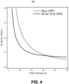
- FIG. 4 is a plot 400 showing the correlation between the Ge composition and the SiGe thickness for given XRF and XPS intensities as described by equations (1) through (3) of Figures 3A and 3B .
- Plot 400 also graphically demonstrates how a unique solution can be found to determine Ge% and SiGe thickness, by using both the XPS and XRF signals.
- the dashed curve of plot 400 represents all the possible Ge% and SiGe thickness solutions for a given Ge fluorescence intensity.
- Figure 5 includes plots 502, 504, 506 showing examples of the XPS (Ge3d region), XPS (Si2p region) and the XRF (GeL ⁇ ) spectra, respectively, as acquired simultaneously from a SiGe/Si sample, in accordance with an embodiment of the present invention.
- the Ge3d region may exhibit peaks from Ge-0 and 02s (plot 502).
- a Si-0 peak is observed (plot 504), where the signal originates from native oxide at the surface.
- the GeL ⁇ XRF signal can be observed at around 1230eV (plot 506).
- the extraction of the XPS and XRF intensities is accomplished using well-established methods of background subtraction and Gaussian/Gauss- Lorentz peak fitting.
- pure Gaussian multi-peak fitting typically leads to goodness of fit (GOF) fit-quality values of 0.97.
- a set of design of experiment (DOE) wafers was generated with various SiGe composition and thicknesses.
- the DOE consisted of 17 wafers with six different SiGe thickness splits over a wide range, and four composition splits with less than 5% atomic composition (AC) difference.
- the sensitivity of the XPS-XRF measurement on SiGe was investigated, along with its applicability over much thicker films, such as films greater than approximately 150 Angstroms. The validity of the film analysis model was also tested. Measurements were taken at both nine sites and 21 sites per wafer, but it was found that the results were very similar.
- Figure 6 includes the normalized measured values plotted against the nominal composition (plot 602) and thicknesses (plot 604), in accordance with an embodiment of the present invention.
- plots of normalized measured Ge% AC (plot 602) and SiGe thickness (plot 604) versus the targeted values are provided.
- the plots show an excellent correlation between the measured and targeted values, with a slope close to 1.0, and R 2 >0.97. Accordingly, the measurements are highly sensitive to process change. Additionally, data indicate that the composition and thickness measurements are decoupled.
- the results also indicate that the film stack model using both XPS and XRF signals, represented by Figure 2 and Equations (1) through (3) of Figures 3A and 3B , represents the SiGe/Si system very well.
- FIG. 7 includes plots showing good linearity between XPS measured SiGe atomic composition (plot 702) and SiGe thickness (plot 704) to an XRD reference, in accordance with an embodiment of the present invention.
- the two measurements correlate very well and are highly linear over a wide range of thickness and composition. From the measurement of such thicker SiGe films, which are traditionally too thick for XPS measurement, in accordance with one or more embodiments described herein, it is shown that simultaneous XRF-XPS metrology can extend traditional XPS capabilities. In one such embodiment, however, extending the capabilities involves the assumption that the SiGe composition remains constant over the entire film.
- UTBB ultra-thin body and buried oxide
- FDSOI fully depleted silicon on insulator
- a pFET channel of such a device may be compressively strained with SiGe.
- Ge enrichment can be used to generate SiGe on insulator samples and achieve a thin compressive strained layer.
- Ge enrichment is initiated with a thin oxide layer deposited to stabilize the surface of the SiGe layer, followed by a standard rapid thermal oxidation (RTO) process to oxidize the SiGe and push the Ge atoms in the underlying SOI, yielding approximately 7nm SGOI containing a range of approximately 15-35% Ge.
- RTO rapid thermal oxidation
- a UTBB SiGe application can be used in the precision evaluation of the combined XPS-XRF metrology tool.
- both static and dynamic precision were evaluated with UTBB FDSOI product wafers.
- the measurements were performed on 50 ⁇ m 2 metrology boxes to evaluate factors such as x-ray beam size consistency and spillage that might affect the precision of product wafer measurement in high volume production.
- Static precision also known as measurement repeatability
- Dynamic precision also known as measurement reproducibility
- the standard deviation of each measurement site was first determined separately, and then the relative standard deviation (RSD) of the five sites were averaged. Accordingly, the precision is reported in terms of RSD of the mean value.
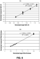
- Figure 8A includes plots of SiGe thickness (plot 802) and Ge% (plot 804) from a static precision measurement.
- Figure 8B includes plots of SiGe thickness (plot 852) and Ge% (plot 854) from a dynamic precision measurement.
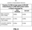
- the normalized wafer average of SiGe thickness and Ge% AC over a period of 4 months shows that the measurements are very stable, with SiGe thickness RSD at approximately 0.53%, and Ge% AC RSD at approximately 0.33%.
- the values are also tabulated in Table 900 of Figure 9 .
- metrology for SiGe related process technology in a high volume manufacturing environment can be achieved with ease, while maintaining the sensitivity, precision and stability of the measurements.
- silicon germanium composition and thickness determination can be made via simultaneous small-spot XPS and XRF Measurements.
- the thickness and composition determination of SiGe films may be made using simultaneous XPS and XRF measurements. Measurements of SiGe films in various applications have been explored, as described above. The measurements are sensitive and linear over a much wider range of SiGe thickness, with excellent precision. Long term stability of the measurement is also shown to be very good.
- Embodiments of the present invention may be provided as a computer program product, or software, that may include a machine-readable medium having stored thereon instructions, which may be used to program a computer system (or other electronic devices) to perform a process according to an embodiment of the present invention.
- the computer system is coupled with the XPS+XRF combination tool described in association with Figure 1 .
- a machine-readable medium includes any mechanism for storing or transmitting information in a form readable by a machine (e.g., a computer).
- a machine- readable (e.g., computer-readable) medium includes a machine (e.g., a computer) readable storage medium (e.g., read only memory (“ROM”), random access memory (“RAM”), magnetic disk storage media, optical storage media, flash memory devices, etc.), a machine (e.g., computer) readable transmission medium (electrical, optical, acoustical or other form of propagated signals (e.g., infrared signals, digital signals, etc.)), etc.
- Figure 11 illustrates a diagrammatic representation of a machine in the exemplary form of a computer system 1100 within which a set of instructions, for causing the machine to perform any one or more of the methodologies discussed herein, may be executed.
- the machine may be connected (e.g., networked) to other machines in a Local Area Network (LAN), an intranet, an extranet, or the Internet.
- LAN Local Area Network
- the machine may operate in the capacity of a server or a client machine in a client- server network environment, or as a peer machine in a peer-to-peer (or distributed) network environment.
- the machine may be a personal computer (PC), a tablet PC, a set-top box (STB), a Personal Digital Assistant (PDA), a cellular telephone, a web appliance, a server, a network router, switch or bridge, or any machine capable of executing a set of instructions (sequential or otherwise) that specify actions to be taken by that machine.
- PC personal computer
- PDA Personal Digital Assistant
- STB set-top box
- WPA Personal Digital Assistant
- a cellular telephone a web appliance
- server e.g., a server
- network router e.g., switch or bridge
- any machine capable of executing a set of instructions (sequential or otherwise) that specify actions to be taken by that machine.
- the term "machine” shall also be taken to include any collection of machines (e.g., computers) that individually or jointly execute a set (or multiple sets) of instructions to perform any one or more of the methodologies discussed herein.
- a machine is configured to execute one or more sets of instruction for calibr
- the exemplary computer system 1100 includes a processor 1102, a main memory 1104 (e.g., read-only memory (ROM), flash memory, dynamic random access memory (DRAM) such as synchronous DRAM (SDRAM) or Rambus DRAM (RDRAM), etc.), a static memory 1106 (e.g., flash memory, static random access memory (SRAM), etc.), and a secondary memory 1118 (e.g., a data storage device), which communicate with each other via a bus 1130.
- main memory 1104 e.g., read-only memory (ROM), flash memory, dynamic random access memory (DRAM) such as synchronous DRAM (SDRAM) or Rambus DRAM (RDRAM), etc.
- DRAM dynamic random access memory
- SDRAM synchronous DRAM
- RDRAM Rambus DRAM
- static memory 1106 e.g., flash memory, static random access memory (SRAM), etc.
- secondary memory 1118 e.g., a data storage device
- Processor 1102 represents one or more general -purpose processing devices such as a microprocessor, central processing unit, or the like. More particularly, the processor 1102 may be a complex instruction set computing (CISC) microprocessor, reduced instruction set computing (RISC) microprocessor, very long instruction word (VLIW) microprocessor, processor implementing other instruction sets, or processors implementing a combination of instruction sets. Processor 1102 may also be one or more special-purpose processing devices such as an application specific integrated circuit (ASIC), a field programmable gate array (FPGA), a digital signal processor (DSP), network processor, or the like. Processor 1102 is configured to execute the processing logic 1126 for performing the operations discussed herein.
- ASIC application specific integrated circuit
- FPGA field programmable gate array
- DSP digital signal processor
- the computer system 1100 may further include a network interface device 1108.
- the computer system 1100 also may include a video display unit 1110 (e.g., a liquid crystal display (LCD) or a cathode ray tube (CRT)), an alphanumeric input device 1112 (e.g., a keyboard), a cursor control device 1114 (e.g., a mouse), and a signal generation device 1116 (e.g., a speaker).
- a video display unit 1110 e.g., a liquid crystal display (LCD) or a cathode ray tube (CRT)
- an alphanumeric input device 1112 e.g., a keyboard
- a cursor control device 1114 e.g., a mouse
- a signal generation device 1116 e.g., a speaker
- the secondary memory 1118 may include a machine-accessible storage medium (or more specifically a computer-readable storage medium) 1131 on which is stored one or more sets of instructions (e.g., software 1122) embodying any one or more of the methodologies or functions described herein.
- the software 1122 may also reside, completely or at least partially, within the main memory 1104 and/or within the processor 1102 during execution thereof by the computer system 1100, the main memory 1104 and the processor 1102 also constituting machine-readable storage media.
- the software 1122 may further be transmitted or received over a network 1120 via the network interface device 1108.
- machine-accessible storage medium 1131 is shown in an exemplary embodiment to be a single medium, the term “machine-readable storage medium” should be taken to include a single medium or multiple media (e.g., a centralized or distributed database, and/or associated caches and servers) that store the one or more sets of instructions.
- the term “machine-readable storage medium” shall also be taken to include any medium that is capable of storing or encoding a set of instructions for execution by the machine and that cause the machine to perform any one or more of the methodologies of the present invention.
- the term “machine- readable storage medium” shall accordingly be taken to include, but not be limited to, solid-state memories, and optical and magnetic media.
Landscapes
- Physics & Mathematics (AREA)
- General Physics & Mathematics (AREA)
- Chemical & Material Sciences (AREA)
- General Health & Medical Sciences (AREA)
- Health & Medical Sciences (AREA)
- Life Sciences & Earth Sciences (AREA)
- Analytical Chemistry (AREA)
- Biochemistry (AREA)
- Immunology (AREA)
- Pathology (AREA)
- Spectroscopy & Molecular Physics (AREA)
- Electromagnetism (AREA)
- Dispersion Chemistry (AREA)
- Analysing Materials By The Use Of Radiation (AREA)
Claims (13)
- Verfahren zum Charakterisieren eines Siliziumgermaniumfilms, wobei das Verfahren Folgendes umfasst:Erzeugen eines Röntgenstrahls;Positionieren einer Probe in einem Pfad des Röntgenstrahls;Sammeln eines Röntgen-Photoelektronenspektroskopiesignals (XPS-Signal), das durch Bombardieren der Probe mit dem Röntgenstrahl erzeugt wird;Sammeln eines Röntgenfluoreszenzsignals (XRF-Signal), das durch Bombardieren der Probe mit dem Röntgenstrahl erzeugt wird; undBestimmen einer Zusammensetzung des Siliziumgermaniumfilms aus dem XRF-Signal und dem XPS-Signal, gekennzeichnet durch Bestimmen der Zusammensetzung eines Siliziumgermaniumdünnfilms auf Si-haltigem Substrat mit Hilfe eines Vergleichs des XRF-Signals und des XPS-Signals mit einem realistischen Materialschichtmischmodell, das die vorhergesagte Intensität eines XRF-Ge-Signals und eines XPS-Ge-Signals relativ zu einem reinen Germaniumfilm skaliert, wodurch die verbleibende Fraktion des Siliziumgermaniumfilms auf Si beschränkt wird.
- Verfahren nach Anspruch 1, weiter umfassend:
Bestimmen einer Dicke des Siliziumgermaniumfilms aus dem XRF-Signal und dem XPS-Signal. - Verfahren nach Ansprüchen 1 und 2, wobei Sammeln des XPS-Signals und Sammeln des XRF-Signals gleichzeitig durchgeführt werden.
- Verfahren nach Anspruch 1, wobei Sammeln des XPS-Signals und Sammeln des XRF-Signals Sammeln innerhalb einer ungefähr 50 µm2 Messbox der Probe umfasst.
- Verfahren nach Anspruch 1, wobei Bestimmen der Dicke des Siliziumgermaniumfilms Bestimmen der Dicke einer Siliziumgermaniumkanalschicht einer Halbleitervorrichtung umfasst.
- Verfahren nach Anspruch 1, wobei Bestimmen der Dicke des Siliziumgermaniumfilms Bestimmen der Dicke eines Siliziumgermanium-Source- oder Drain-Gebiets einer Halbleitervorrichtung umfasst.
- System zum Charakterisieren eines Siliziumgermaniumfilms, wobei das System Folgendes umfasst:eine Röntgenquelle zum Erzeugen eines Röntgenstrahls;eine Probenhalterung zum Positionieren einer Probe in einem Pfad des Röntgenstrahls;einen ersten Detektor zum Sammeln eines Röntgen-Photoelektronenspektroskopiesignals (XPS-Signal), das durch Bombardieren der Probe mit dem Röntgenstrahl erzeugt wird; und einen zweiten Detektor zum Sammeln eines Röntgenfluoreszenzsignals (XRF-Signal), das durch Bombardieren der Probe mit dem Röntgenstrahl erzeugt wird, wobei das XRF-Signal und das XPS-Signal zum Bestimmen einer Zusammensetzung des Siliziumgermaniumfilms dienen, dadurch gekennzeichnet, dass das System ausgelegt ist, die Zusammensetzung eines Siliziumgermaniumdünnfilms auf Si-haltigem Substrat mit Hilfe eines Vergleichs des XRF-Signals und des XPS-Signals mit einem realistischen Materialschichtmischmodell zu bestimmen, das die vorhergesagte Intensität eines XRF-Ge-Signals und eines XPS-Ge-Signals relativ zu einem reinen Germaniumfilm skaliert, wodurch die verbleibende Fraktion des Siliziumgermaniumfilms auf Si beschränkt wird.
- System nach Anspruch 7, wobei der erste Detektor und der zweite Detektor ausgelegt sind, das XPS-Signal beziehungsweise das XRF-Signal zum gleichen Zeitpunkt zu sammeln.
- System nach Anspruch 7, wobei der erste Detektor und der zweite Detektor ausgelegt sind, das XPS-Signal beziehungsweise das XRF-Signal innerhalb einer ungefähr 50 µm2 Messbox der Probe zu sammeln.
- System nach Anspruch 8, weiter umfassend:
einen Post-Monochromator-Flussdetektor zum Normieren des XRF-Signals in Bezug auf einen eingehenden Röntgenfluss für eine stabile Messung. - System nach Anspruch 7, wobei das System während des Sammelns des XPS-Signals und des XRF-Signals unter einem Basisdruck von weniger als etwa 1,33E-7 mbar (1,0E-7 Torr) gehalten wird.
- System nach Anspruch 7, wobei der Röntgenstrahl ein monochromatischer AlKa-Röntgenstrahl ist.
- System nach Anspruch 7, weiter umfassend einen Quarzmonochromator, der entlang des Pfades des Röntgenstrahls zwischen der Röntgenquelle und der Probenhalterung angeordnet ist.
Applications Claiming Priority (3)
| Application Number | Priority Date | Filing Date | Title |
|---|---|---|---|
| US201461984286P | 2014-04-25 | 2014-04-25 | |
| US14/691,164 US9594035B2 (en) | 2014-04-25 | 2015-04-20 | Silicon germanium thickness and composition determination using combined XPS and XRF technologies |
| PCT/US2015/026935 WO2015164417A1 (en) | 2014-04-25 | 2015-04-21 | Silicon germanium thickness and composition determination using combined xps and xrf technologies |
Publications (3)
| Publication Number | Publication Date |
|---|---|
| EP3134712A1 EP3134712A1 (de) | 2017-03-01 |
| EP3134712A4 EP3134712A4 (de) | 2017-11-08 |
| EP3134712B1 true EP3134712B1 (de) | 2023-05-31 |
Family
ID=54333103
Family Applications (1)
| Application Number | Title | Priority Date | Filing Date |
|---|---|---|---|
| EP15782815.3A Active EP3134712B1 (de) | 2014-04-25 | 2015-04-21 | Bestimmung der dicke und zusammensetzung von silicium-germanium mit kombinierter xps- und xrf-technologie |
Country Status (6)
| Country | Link |
|---|---|
| US (2) | US9594035B2 (de) |
| EP (1) | EP3134712B1 (de) |
| KR (1) | KR102323746B1 (de) |
| CN (2) | CN115388950B (de) |
| TW (2) | TWI653446B (de) |
| WO (1) | WO2015164417A1 (de) |
Cited By (1)
| Publication number | Priority date | Publication date | Assignee | Title |
|---|---|---|---|---|
| US20240418633A1 (en) * | 2023-06-16 | 2024-12-19 | Kla Corporation | Combination of multiwavelength raman and spectroscopic ellipsometry to measure a film stack |
Families Citing this family (16)
| Publication number | Priority date | Publication date | Assignee | Title |
|---|---|---|---|---|
| KR102527483B1 (ko) | 2014-06-24 | 2023-04-28 | 리베라 인코퍼레이티드 | Xps 및 xrf 기법을 이용하는 다중-층 및 다중-프로세스의 피드-포워드 |
| US10012606B1 (en) * | 2014-06-24 | 2018-07-03 | Kla-Tencor Corporation | X-ray based metrology with primary and secondary illumination sources |
| SE540581C2 (en) * | 2015-05-08 | 2018-10-02 | Hard X-Ray Photoelectron Spectroscopy Apparatus | |
| KR102929314B1 (ko) * | 2015-11-02 | 2026-02-24 | 노바 메주어링 인스트루먼트 인크. | 비파괴적 박막 측정 방법 및 시스템 |
| US10895541B2 (en) | 2018-01-06 | 2021-01-19 | Kla-Tencor Corporation | Systems and methods for combined x-ray reflectometry and photoelectron spectroscopy |
| US11703464B2 (en) * | 2018-07-28 | 2023-07-18 | Bruker Technologies Ltd. | Small-angle x-ray scatterometry |
| US11295969B2 (en) | 2018-11-27 | 2022-04-05 | International Business Machines Corporation | Hybridization for characterization and metrology |
| US11852467B2 (en) | 2019-03-12 | 2023-12-26 | Nova Measuring Instruments, Inc. | Method and system for monitoring deposition process |
| CN109931894B (zh) * | 2019-03-26 | 2021-02-02 | 电子科技大学 | 一种NiFe或FeMn薄膜表面氧化层厚度的分析方法 |
| CN109901058B (zh) * | 2019-03-29 | 2021-04-02 | 上海华力集成电路制造有限公司 | 一种半导体器件的分析方法 |
| CN110596174B (zh) * | 2019-09-04 | 2021-03-30 | 电子科技大学 | 一种用于评估高反射率膜损耗稳定性的测试方法 |
| KR102926510B1 (ko) * | 2020-05-26 | 2026-02-10 | 삼성전자주식회사 | 엑스선 광전자 분광법을 이용한 그래핀층의 두께 계산방법 및 실리콘 카바이드의 함량 측정 방법 |
| JP7596184B2 (ja) | 2021-03-11 | 2024-12-09 | 株式会社東芝 | 官能基密度測定方法 |
| KR20240152817A (ko) * | 2021-10-24 | 2024-10-22 | 노바 메주어링 인스트루먼트 인크. | 멀티 측정값이 있는 xps를 사용한 소형 박스에서의 특성화 및 측정 |
| CN115791862B (zh) * | 2022-12-22 | 2024-03-26 | 南开大学 | 一种晶圆表面量测设备、检测方法及应用 |
| US12436123B2 (en) * | 2023-09-06 | 2025-10-07 | Schlumberger Technology Corporation | XRF measurements of multiphase oilfield fluids |
Family Cites Families (19)
| Publication number | Priority date | Publication date | Assignee | Title |
|---|---|---|---|---|
| US6891158B2 (en) * | 2002-12-27 | 2005-05-10 | Revera Incorporated | Nondestructive characterization of thin films based on acquired spectrum |
| JP2004347406A (ja) * | 2003-05-21 | 2004-12-09 | Toyota Motor Corp | 表面分析用粉末試料成形治具および表面分析用粉末試料成形方法 |
| JP4202217B2 (ja) | 2003-09-05 | 2008-12-24 | 三井化学株式会社 | 光学薄膜、それを用いた表示装置および画像を作成する方法 |
| US7120228B2 (en) * | 2004-09-21 | 2006-10-10 | Jordan Valley Applied Radiation Ltd. | Combined X-ray reflectometer and diffractometer |
| US7358494B1 (en) | 2005-06-15 | 2008-04-15 | Kla-Tencor Technologies Corporation | Material composition analysis system and method |
| CA2623927A1 (en) * | 2005-10-04 | 2007-04-12 | Thermo Niton Analyzers Llc | Analysis of elemental composition and thickness in multilayered materials |
| RU2009120540A (ru) * | 2006-11-01 | 2010-12-10 | Дау Глобал Текнолоджиз Инк. (Us) | Формованные пористые элементы из альфа-оксида алюминия и способы их получения |
| US7440541B2 (en) | 2006-12-27 | 2008-10-21 | Innov-X-Systems, Inc. | Dual source XRF system |
| RU2010152658A (ru) * | 2008-05-23 | 2012-06-27 | Те Острейлиан Нэшнл Юниверсити (Au) | Обработка данных изображения |
| US7929667B1 (en) * | 2008-10-02 | 2011-04-19 | Kla-Tencor Corporation | High brightness X-ray metrology |
| CN102272878B (zh) * | 2008-10-31 | 2014-07-23 | Fei公司 | 样本厚度的测量和终点确定 |
| US8513603B1 (en) * | 2010-05-12 | 2013-08-20 | West Virginia University | In-situ determination of thin film and multilayer structure and chemical composition using x-ray fluorescence induced by grazing incidence electron beams during thin film growth |
| WO2012024509A1 (en) | 2010-08-20 | 2012-02-23 | First Solar, Inc. | Position-sensitive metrology system |
| JP5871263B2 (ja) * | 2011-06-14 | 2016-03-01 | 富士フイルム株式会社 | 非晶質酸化物薄膜の製造方法 |
| MX2011009486A (es) | 2011-09-09 | 2013-03-15 | Ct Investig Y Estudios Del Ipn | Metodo combinado de espectroscopias de masas de iones secundarios y de rayos x de energia dispersada, para analisis quimico cuantitativo de diversos materiales solidos y peliculas delgadas. |
| US9240254B2 (en) * | 2011-09-27 | 2016-01-19 | Revera, Incorporated | System and method for characterizing a film by X-ray photoelectron and low-energy X-ray fluorescence spectroscopy |
| US10013518B2 (en) * | 2012-07-10 | 2018-07-03 | Kla-Tencor Corporation | Model building and analysis engine for combined X-ray and optical metrology |
| KR101241007B1 (ko) | 2012-10-26 | 2013-03-11 | 나노씨엠에스(주) | 엑스선을 이용한 박막층의 두께 측정 방법 및 장치 |
| US9535018B2 (en) * | 2013-07-08 | 2017-01-03 | Kla-Tencor Corporation | Combined x-ray and optical metrology |
-
2015
- 2015-04-20 US US14/691,164 patent/US9594035B2/en active Active
- 2015-04-21 CN CN202211049485.4A patent/CN115388950B/zh active Active
- 2015-04-21 WO PCT/US2015/026935 patent/WO2015164417A1/en not_active Ceased
- 2015-04-21 KR KR1020167032758A patent/KR102323746B1/ko active Active
- 2015-04-21 EP EP15782815.3A patent/EP3134712B1/de active Active
- 2015-04-21 CN CN201580032862.5A patent/CN106461428A/zh active Pending
- 2015-04-24 TW TW107127928A patent/TWI653446B/zh active
- 2015-04-24 TW TW104113178A patent/TWI641829B/zh active
-
2017
- 2017-03-09 US US15/454,950 patent/US9952166B2/en active Active
Cited By (1)
| Publication number | Priority date | Publication date | Assignee | Title |
|---|---|---|---|---|
| US20240418633A1 (en) * | 2023-06-16 | 2024-12-19 | Kla Corporation | Combination of multiwavelength raman and spectroscopic ellipsometry to measure a film stack |
Also Published As
| Publication number | Publication date |
|---|---|
| KR20160147902A (ko) | 2016-12-23 |
| EP3134712A4 (de) | 2017-11-08 |
| CN106461428A (zh) | 2017-02-22 |
| US9952166B2 (en) | 2018-04-24 |
| TW201621303A (zh) | 2016-06-16 |
| CN115388950A (zh) | 2022-11-25 |
| EP3134712A1 (de) | 2017-03-01 |
| TW201839390A (zh) | 2018-11-01 |
| TWI641829B (zh) | 2018-11-21 |
| TWI653446B (zh) | 2019-03-11 |
| US20170176357A1 (en) | 2017-06-22 |
| US9594035B2 (en) | 2017-03-14 |
| WO2015164417A1 (en) | 2015-10-29 |
| US20150308969A1 (en) | 2015-10-29 |
| KR102323746B1 (ko) | 2021-11-09 |
| CN115388950B (zh) | 2024-10-18 |
Similar Documents
| Publication | Publication Date | Title |
|---|---|---|
| EP3134712B1 (de) | Bestimmung der dicke und zusammensetzung von silicium-germanium mit kombinierter xps- und xrf-technologie | |
| US20240085174A1 (en) | Feed-forward of multi-layer and multi-process information using xps and xrf technologies | |
| EP2761284B1 (de) | System und verfahren zur charakterisierung eines films durch röntgenstrahlphotoelektronen und niederenergetische röntgenfluoreszenzspektroskopie | |
| Anagnostopoulos et al. | Characterization of aluminum nitride based films with high resolution X-ray fluorescence spectroscopy | |
| Grande et al. | Determination of thickness and composition of high-k dielectrics using high-energy electrons | |
| L'herron et al. | Silicon-Germanium (SiGe) composition and thickness determination via simultaneous smallspot XPS and XRF measurements | |
| JP4537149B2 (ja) | 蛍光x線分析方法 | |
| Martinez et al. | Germanium out diffusion in SiGe-based HfO2 gate stacks | |
| Sparks et al. | Characterizing process semiconductor thin films with a confocal micro X-ray fluorescence microscope | |
| Martinez et al. | Lanthanum quantification for optimization of advanced high-k/metal gate stacks using low energy electron x-ray emission spectrometry |
Legal Events
| Date | Code | Title | Description |
|---|---|---|---|
| STAA | Information on the status of an ep patent application or granted ep patent |
Free format text: STATUS: THE INTERNATIONAL PUBLICATION HAS BEEN MADE |
|
| PUAI | Public reference made under article 153(3) epc to a published international application that has entered the european phase |
Free format text: ORIGINAL CODE: 0009012 |
|
| STAA | Information on the status of an ep patent application or granted ep patent |
Free format text: STATUS: REQUEST FOR EXAMINATION WAS MADE |
|
| 17P | Request for examination filed |
Effective date: 20161115 |
|
| AK | Designated contracting states |
Kind code of ref document: A1 Designated state(s): AL AT BE BG CH CY CZ DE DK EE ES FI FR GB GR HR HU IE IS IT LI LT LU LV MC MK MT NL NO PL PT RO RS SE SI SK SM TR |
|
| AX | Request for extension of the european patent |
Extension state: BA ME |
|
| DAV | Request for validation of the european patent (deleted) | ||
| DAX | Request for extension of the european patent (deleted) | ||
| A4 | Supplementary search report drawn up and despatched |
Effective date: 20171009 |
|
| RIC1 | Information provided on ipc code assigned before grant |
Ipc: G01B 15/02 20060101ALI20171002BHEP Ipc: G01N 23/22 20060101ALI20171002BHEP Ipc: G01N 23/223 20060101ALI20171002BHEP Ipc: G01N 23/227 20060101ALI20171002BHEP Ipc: G01D 21/02 20060101AFI20171002BHEP |
|
| RAP1 | Party data changed (applicant data changed or rights of an application transferred) |
Owner name: NOVA MEASURING INSTRUMENTS, INC. |
|
| STAA | Information on the status of an ep patent application or granted ep patent |
Free format text: STATUS: EXAMINATION IS IN PROGRESS |
|
| 17Q | First examination report despatched |
Effective date: 20210607 |
|
| GRAP | Despatch of communication of intention to grant a patent |
Free format text: ORIGINAL CODE: EPIDOSNIGR1 |
|
| STAA | Information on the status of an ep patent application or granted ep patent |
Free format text: STATUS: GRANT OF PATENT IS INTENDED |
|
| INTG | Intention to grant announced |
Effective date: 20221214 |
|
| GRAS | Grant fee paid |
Free format text: ORIGINAL CODE: EPIDOSNIGR3 |
|
| GRAA | (expected) grant |
Free format text: ORIGINAL CODE: 0009210 |
|
| STAA | Information on the status of an ep patent application or granted ep patent |
Free format text: STATUS: THE PATENT HAS BEEN GRANTED |
|
| AK | Designated contracting states |
Kind code of ref document: B1 Designated state(s): AL AT BE BG CH CY CZ DE DK EE ES FI FR GB GR HR HU IE IS IT LI LT LU LV MC MK MT NL NO PL PT RO RS SE SI SK SM TR |
|
| REG | Reference to a national code |
Ref country code: GB Ref legal event code: FG4D Ref country code: CH Ref legal event code: EP |
|
| REG | Reference to a national code |
Ref country code: AT Ref legal event code: REF Ref document number: 1571174 Country of ref document: AT Kind code of ref document: T Effective date: 20230615 Ref country code: DE Ref legal event code: R096 Ref document number: 602015083748 Country of ref document: DE |
|
| REG | Reference to a national code |
Ref country code: IE Ref legal event code: FG4D |
|
| REG | Reference to a national code |
Ref country code: LT Ref legal event code: MG9D |
|
| REG | Reference to a national code |
Ref country code: NL Ref legal event code: MP Effective date: 20230531 |
|
| REG | Reference to a national code |
Ref country code: AT Ref legal event code: MK05 Ref document number: 1571174 Country of ref document: AT Kind code of ref document: T Effective date: 20230531 |
|
| PG25 | Lapsed in a contracting state [announced via postgrant information from national office to epo] |
Ref country code: SE Free format text: LAPSE BECAUSE OF FAILURE TO SUBMIT A TRANSLATION OF THE DESCRIPTION OR TO PAY THE FEE WITHIN THE PRESCRIBED TIME-LIMIT Effective date: 20230531 Ref country code: NO Free format text: LAPSE BECAUSE OF FAILURE TO SUBMIT A TRANSLATION OF THE DESCRIPTION OR TO PAY THE FEE WITHIN THE PRESCRIBED TIME-LIMIT Effective date: 20230831 Ref country code: ES Free format text: LAPSE BECAUSE OF FAILURE TO SUBMIT A TRANSLATION OF THE DESCRIPTION OR TO PAY THE FEE WITHIN THE PRESCRIBED TIME-LIMIT Effective date: 20230531 Ref country code: AT Free format text: LAPSE BECAUSE OF FAILURE TO SUBMIT A TRANSLATION OF THE DESCRIPTION OR TO PAY THE FEE WITHIN THE PRESCRIBED TIME-LIMIT Effective date: 20230531 |
|
| PG25 | Lapsed in a contracting state [announced via postgrant information from national office to epo] |
Ref country code: RS Free format text: LAPSE BECAUSE OF FAILURE TO SUBMIT A TRANSLATION OF THE DESCRIPTION OR TO PAY THE FEE WITHIN THE PRESCRIBED TIME-LIMIT Effective date: 20230531 Ref country code: PL Free format text: LAPSE BECAUSE OF FAILURE TO SUBMIT A TRANSLATION OF THE DESCRIPTION OR TO PAY THE FEE WITHIN THE PRESCRIBED TIME-LIMIT Effective date: 20230531 Ref country code: NL Free format text: LAPSE BECAUSE OF FAILURE TO SUBMIT A TRANSLATION OF THE DESCRIPTION OR TO PAY THE FEE WITHIN THE PRESCRIBED TIME-LIMIT Effective date: 20230531 Ref country code: LV Free format text: LAPSE BECAUSE OF FAILURE TO SUBMIT A TRANSLATION OF THE DESCRIPTION OR TO PAY THE FEE WITHIN THE PRESCRIBED TIME-LIMIT Effective date: 20230531 Ref country code: LT Free format text: LAPSE BECAUSE OF FAILURE TO SUBMIT A TRANSLATION OF THE DESCRIPTION OR TO PAY THE FEE WITHIN THE PRESCRIBED TIME-LIMIT Effective date: 20230531 Ref country code: IS Free format text: LAPSE BECAUSE OF FAILURE TO SUBMIT A TRANSLATION OF THE DESCRIPTION OR TO PAY THE FEE WITHIN THE PRESCRIBED TIME-LIMIT Effective date: 20230930 Ref country code: HR Free format text: LAPSE BECAUSE OF FAILURE TO SUBMIT A TRANSLATION OF THE DESCRIPTION OR TO PAY THE FEE WITHIN THE PRESCRIBED TIME-LIMIT Effective date: 20230531 Ref country code: GR Free format text: LAPSE BECAUSE OF FAILURE TO SUBMIT A TRANSLATION OF THE DESCRIPTION OR TO PAY THE FEE WITHIN THE PRESCRIBED TIME-LIMIT Effective date: 20230901 |
|
| PG25 | Lapsed in a contracting state [announced via postgrant information from national office to epo] |
Ref country code: FI Free format text: LAPSE BECAUSE OF FAILURE TO SUBMIT A TRANSLATION OF THE DESCRIPTION OR TO PAY THE FEE WITHIN THE PRESCRIBED TIME-LIMIT Effective date: 20230531 |
|
| PG25 | Lapsed in a contracting state [announced via postgrant information from national office to epo] |
Ref country code: SK Free format text: LAPSE BECAUSE OF FAILURE TO SUBMIT A TRANSLATION OF THE DESCRIPTION OR TO PAY THE FEE WITHIN THE PRESCRIBED TIME-LIMIT Effective date: 20230531 |
|
| PG25 | Lapsed in a contracting state [announced via postgrant information from national office to epo] |
Ref country code: SM Free format text: LAPSE BECAUSE OF FAILURE TO SUBMIT A TRANSLATION OF THE DESCRIPTION OR TO PAY THE FEE WITHIN THE PRESCRIBED TIME-LIMIT Effective date: 20230531 Ref country code: SK Free format text: LAPSE BECAUSE OF FAILURE TO SUBMIT A TRANSLATION OF THE DESCRIPTION OR TO PAY THE FEE WITHIN THE PRESCRIBED TIME-LIMIT Effective date: 20230531 Ref country code: RO Free format text: LAPSE BECAUSE OF FAILURE TO SUBMIT A TRANSLATION OF THE DESCRIPTION OR TO PAY THE FEE WITHIN THE PRESCRIBED TIME-LIMIT Effective date: 20230531 Ref country code: PT Free format text: LAPSE BECAUSE OF FAILURE TO SUBMIT A TRANSLATION OF THE DESCRIPTION OR TO PAY THE FEE WITHIN THE PRESCRIBED TIME-LIMIT Effective date: 20231002 Ref country code: EE Free format text: LAPSE BECAUSE OF FAILURE TO SUBMIT A TRANSLATION OF THE DESCRIPTION OR TO PAY THE FEE WITHIN THE PRESCRIBED TIME-LIMIT Effective date: 20230531 Ref country code: DK Free format text: LAPSE BECAUSE OF FAILURE TO SUBMIT A TRANSLATION OF THE DESCRIPTION OR TO PAY THE FEE WITHIN THE PRESCRIBED TIME-LIMIT Effective date: 20230531 Ref country code: CZ Free format text: LAPSE BECAUSE OF FAILURE TO SUBMIT A TRANSLATION OF THE DESCRIPTION OR TO PAY THE FEE WITHIN THE PRESCRIBED TIME-LIMIT Effective date: 20230531 |
|
| REG | Reference to a national code |
Ref country code: DE Ref legal event code: R097 Ref document number: 602015083748 Country of ref document: DE |
|
| PLBE | No opposition filed within time limit |
Free format text: ORIGINAL CODE: 0009261 |
|
| STAA | Information on the status of an ep patent application or granted ep patent |
Free format text: STATUS: NO OPPOSITION FILED WITHIN TIME LIMIT |
|
| PG25 | Lapsed in a contracting state [announced via postgrant information from national office to epo] |
Ref country code: SI Free format text: LAPSE BECAUSE OF FAILURE TO SUBMIT A TRANSLATION OF THE DESCRIPTION OR TO PAY THE FEE WITHIN THE PRESCRIBED TIME-LIMIT Effective date: 20230531 |
|
| 26N | No opposition filed |
Effective date: 20240301 |
|
| PG25 | Lapsed in a contracting state [announced via postgrant information from national office to epo] |
Ref country code: SI Free format text: LAPSE BECAUSE OF FAILURE TO SUBMIT A TRANSLATION OF THE DESCRIPTION OR TO PAY THE FEE WITHIN THE PRESCRIBED TIME-LIMIT Effective date: 20230531 Ref country code: IT Free format text: LAPSE BECAUSE OF FAILURE TO SUBMIT A TRANSLATION OF THE DESCRIPTION OR TO PAY THE FEE WITHIN THE PRESCRIBED TIME-LIMIT Effective date: 20230531 |
|
| PG25 | Lapsed in a contracting state [announced via postgrant information from national office to epo] |
Ref country code: BG Free format text: LAPSE BECAUSE OF FAILURE TO SUBMIT A TRANSLATION OF THE DESCRIPTION OR TO PAY THE FEE WITHIN THE PRESCRIBED TIME-LIMIT Effective date: 20230531 |
|
| PG25 | Lapsed in a contracting state [announced via postgrant information from national office to epo] |
Ref country code: MC Free format text: LAPSE BECAUSE OF FAILURE TO SUBMIT A TRANSLATION OF THE DESCRIPTION OR TO PAY THE FEE WITHIN THE PRESCRIBED TIME-LIMIT Effective date: 20230531 |
|
| PG25 | Lapsed in a contracting state [announced via postgrant information from national office to epo] |
Ref country code: MC Free format text: LAPSE BECAUSE OF FAILURE TO SUBMIT A TRANSLATION OF THE DESCRIPTION OR TO PAY THE FEE WITHIN THE PRESCRIBED TIME-LIMIT Effective date: 20230531 Ref country code: BG Free format text: LAPSE BECAUSE OF FAILURE TO SUBMIT A TRANSLATION OF THE DESCRIPTION OR TO PAY THE FEE WITHIN THE PRESCRIBED TIME-LIMIT Effective date: 20230531 |
|
| REG | Reference to a national code |
Ref country code: CH Ref legal event code: PL |
|
| PG25 | Lapsed in a contracting state [announced via postgrant information from national office to epo] |
Ref country code: LU Free format text: LAPSE BECAUSE OF NON-PAYMENT OF DUE FEES Effective date: 20240421 |
|
| REG | Reference to a national code |
Ref country code: BE Ref legal event code: MM Effective date: 20240430 |
|
| PG25 | Lapsed in a contracting state [announced via postgrant information from national office to epo] |
Ref country code: LU Free format text: LAPSE BECAUSE OF NON-PAYMENT OF DUE FEES Effective date: 20240421 |
|
| PG25 | Lapsed in a contracting state [announced via postgrant information from national office to epo] |
Ref country code: BE Free format text: LAPSE BECAUSE OF NON-PAYMENT OF DUE FEES Effective date: 20240430 |
|
| PG25 | Lapsed in a contracting state [announced via postgrant information from national office to epo] |
Ref country code: FR Free format text: LAPSE BECAUSE OF NON-PAYMENT OF DUE FEES Effective date: 20240430 |
|
| PG25 | Lapsed in a contracting state [announced via postgrant information from national office to epo] |
Ref country code: FR Free format text: LAPSE BECAUSE OF NON-PAYMENT OF DUE FEES Effective date: 20240430 Ref country code: BE Free format text: LAPSE BECAUSE OF NON-PAYMENT OF DUE FEES Effective date: 20240430 Ref country code: CH Free format text: LAPSE BECAUSE OF NON-PAYMENT OF DUE FEES Effective date: 20240430 |
|
| PG25 | Lapsed in a contracting state [announced via postgrant information from national office to epo] |
Ref country code: IE Free format text: LAPSE BECAUSE OF NON-PAYMENT OF DUE FEES Effective date: 20240421 |
|
| PGFP | Annual fee paid to national office [announced via postgrant information from national office to epo] |
Ref country code: DE Payment date: 20250422 Year of fee payment: 11 |
|
| PGFP | Annual fee paid to national office [announced via postgrant information from national office to epo] |
Ref country code: GB Payment date: 20250423 Year of fee payment: 11 |
|
| PG25 | Lapsed in a contracting state [announced via postgrant information from national office to epo] |
Ref country code: CY Free format text: LAPSE BECAUSE OF FAILURE TO SUBMIT A TRANSLATION OF THE DESCRIPTION OR TO PAY THE FEE WITHIN THE PRESCRIBED TIME-LIMIT; INVALID AB INITIO Effective date: 20150421 |
|
| PG25 | Lapsed in a contracting state [announced via postgrant information from national office to epo] |
Ref country code: HU Free format text: LAPSE BECAUSE OF FAILURE TO SUBMIT A TRANSLATION OF THE DESCRIPTION OR TO PAY THE FEE WITHIN THE PRESCRIBED TIME-LIMIT; INVALID AB INITIO Effective date: 20150421 |