EP3133902B1 - Einstufige leistungsfaktorverbesserte led-treiberschaltung - Google Patents
Einstufige leistungsfaktorverbesserte led-treiberschaltung Download PDFInfo
- Publication number
- EP3133902B1 EP3133902B1 EP16184403.0A EP16184403A EP3133902B1 EP 3133902 B1 EP3133902 B1 EP 3133902B1 EP 16184403 A EP16184403 A EP 16184403A EP 3133902 B1 EP3133902 B1 EP 3133902B1
- Authority
- EP
- European Patent Office
- Prior art keywords
- circuit
- inductor
- node
- current
- electrically connected
- Prior art date
- Legal status (The legal status is an assumption and is not a legal conclusion. Google has not performed a legal analysis and makes no representation as to the accuracy of the status listed.)
- Active
Links
Images


Classifications
-
- H—ELECTRICITY
- H02—GENERATION; CONVERSION OR DISTRIBUTION OF ELECTRIC POWER
- H02M—APPARATUS FOR CONVERSION BETWEEN AC AND AC, BETWEEN AC AND DC, OR BETWEEN DC AND DC, AND FOR USE WITH MAINS OR SIMILAR POWER SUPPLY SYSTEMS; CONVERSION OF DC OR AC INPUT POWER INTO SURGE OUTPUT POWER; CONTROL OR REGULATION THEREOF
- H02M1/00—Details of apparatus for conversion
- H02M1/42—Circuits or arrangements for compensating for or adjusting power factor in converters or inverters
- H02M1/4208—Arrangements for improving power factor of AC input
-
- H—ELECTRICITY
- H02—GENERATION; CONVERSION OR DISTRIBUTION OF ELECTRIC POWER
- H02M—APPARATUS FOR CONVERSION BETWEEN AC AND AC, BETWEEN AC AND DC, OR BETWEEN DC AND DC, AND FOR USE WITH MAINS OR SIMILAR POWER SUPPLY SYSTEMS; CONVERSION OF DC OR AC INPUT POWER INTO SURGE OUTPUT POWER; CONTROL OR REGULATION THEREOF
- H02M7/00—Conversion of AC power input into DC power output; Conversion of DC power input into AC power output
- H02M7/02—Conversion of AC power input into DC power output without possibility of reversal
- H02M7/04—Conversion of AC power input into DC power output without possibility of reversal by static converters
- H02M7/06—Conversion of AC power input into DC power output without possibility of reversal by static converters using discharge tubes without control electrode or semiconductor devices without control electrode
-
- H—ELECTRICITY
- H05—ELECTRIC TECHNIQUES NOT OTHERWISE PROVIDED FOR
- H05B—ELECTRIC HEATING; ELECTRIC LIGHT SOURCES NOT OTHERWISE PROVIDED FOR; CIRCUIT ARRANGEMENTS FOR ELECTRIC LIGHT SOURCES, IN GENERAL
- H05B45/00—Circuit arrangements for operating light-emitting diodes [LED]
- H05B45/40—Details of LED load circuits
- H05B45/44—Details of LED load circuits with an active control inside an LED matrix
- H05B45/48—Details of LED load circuits with an active control inside an LED matrix having LEDs organised in strings and incorporating parallel shunting devices
-
- H—ELECTRICITY
- H05—ELECTRIC TECHNIQUES NOT OTHERWISE PROVIDED FOR
- H05B—ELECTRIC HEATING; ELECTRIC LIGHT SOURCES NOT OTHERWISE PROVIDED FOR; CIRCUIT ARRANGEMENTS FOR ELECTRIC LIGHT SOURCES, IN GENERAL
- H05B47/00—Circuit arrangements for operating light sources in general, i.e. where the type of light source is not relevant
- H05B47/10—Controlling the light source
- H05B47/17—Operational modes, e.g. switching from manual to automatic mode or prohibiting specific operations
-
- H—ELECTRICITY
- H02—GENERATION; CONVERSION OR DISTRIBUTION OF ELECTRIC POWER
- H02M—APPARATUS FOR CONVERSION BETWEEN AC AND AC, BETWEEN AC AND DC, OR BETWEEN DC AND DC, AND FOR USE WITH MAINS OR SIMILAR POWER SUPPLY SYSTEMS; CONVERSION OF DC OR AC INPUT POWER INTO SURGE OUTPUT POWER; CONTROL OR REGULATION THEREOF
- H02M1/00—Details of apparatus for conversion
- H02M1/42—Circuits or arrangements for compensating for or adjusting power factor in converters or inverters
- H02M1/4208—Arrangements for improving power factor of AC input
- H02M1/4225—Arrangements for improving power factor of AC input using a non-isolated boost converter
-
- H—ELECTRICITY
- H05—ELECTRIC TECHNIQUES NOT OTHERWISE PROVIDED FOR
- H05B—ELECTRIC HEATING; ELECTRIC LIGHT SOURCES NOT OTHERWISE PROVIDED FOR; CIRCUIT ARRANGEMENTS FOR ELECTRIC LIGHT SOURCES, IN GENERAL
- H05B45/00—Circuit arrangements for operating light-emitting diodes [LED]
- H05B45/30—Driver circuits
- H05B45/37—Converter circuits
- H05B45/3725—Switched mode power supply [SMPS]
- H05B45/375—Switched mode power supply [SMPS] using buck topology
-
- H—ELECTRICITY
- H05—ELECTRIC TECHNIQUES NOT OTHERWISE PROVIDED FOR
- H05B—ELECTRIC HEATING; ELECTRIC LIGHT SOURCES NOT OTHERWISE PROVIDED FOR; CIRCUIT ARRANGEMENTS FOR ELECTRIC LIGHT SOURCES, IN GENERAL
- H05B45/00—Circuit arrangements for operating light-emitting diodes [LED]
- H05B45/30—Driver circuits
- H05B45/37—Converter circuits
- H05B45/3725—Switched mode power supply [SMPS]
- H05B45/38—Switched mode power supply [SMPS] using boost topology
-
- Y—GENERAL TAGGING OF NEW TECHNOLOGICAL DEVELOPMENTS; GENERAL TAGGING OF CROSS-SECTIONAL TECHNOLOGIES SPANNING OVER SEVERAL SECTIONS OF THE IPC; TECHNICAL SUBJECTS COVERED BY FORMER USPC CROSS-REFERENCE ART COLLECTIONS [XRACs] AND DIGESTS
- Y02—TECHNOLOGIES OR APPLICATIONS FOR MITIGATION OR ADAPTATION AGAINST CLIMATE CHANGE
- Y02B—CLIMATE CHANGE MITIGATION TECHNOLOGIES RELATED TO BUILDINGS, e.g. HOUSING, HOUSE APPLIANCES OR RELATED END-USER APPLICATIONS
- Y02B20/00—Energy efficient lighting technologies, e.g. halogen lamps or gas discharge lamps
- Y02B20/30—Semiconductor lamps, e.g. solid state lamps [SSL] light emitting diodes [LED] or organic LED [OLED]
-
- Y—GENERAL TAGGING OF NEW TECHNOLOGICAL DEVELOPMENTS; GENERAL TAGGING OF CROSS-SECTIONAL TECHNOLOGIES SPANNING OVER SEVERAL SECTIONS OF THE IPC; TECHNICAL SUBJECTS COVERED BY FORMER USPC CROSS-REFERENCE ART COLLECTIONS [XRACs] AND DIGESTS
- Y02—TECHNOLOGIES OR APPLICATIONS FOR MITIGATION OR ADAPTATION AGAINST CLIMATE CHANGE
- Y02B—CLIMATE CHANGE MITIGATION TECHNOLOGIES RELATED TO BUILDINGS, e.g. HOUSING, HOUSE APPLIANCES OR RELATED END-USER APPLICATIONS
- Y02B70/00—Technologies for an efficient end-user side electric power management and consumption
- Y02B70/10—Technologies improving the efficiency by using switched-mode power supplies [SMPS], i.e. efficient power electronics conversion e.g. power factor correction or reduction of losses in power supplies or efficient standby modes
Definitions
- the present invention generally relates to a driver circuit for light emitting diodes (LEDs), and more particularly relates to a single-stage power factor corrected LED driver circuit.
- LEDs light emitting diodes
- One well-known active PFC LED driver is a two-stage Boost-Buck power supply circuit.
- a boost stage acts as a front end PFC due to its smoothly varying input current and simplicity
- buck stage acts as the LED driver.
- this two-stage active PFC LED driver requires two different control circuits to harmonize the input current and to regulate the current through the LEDs.
- the boost stage can exhibit start-up over-currents, which can require additional protection circuitry.
- Another well-known active PFC LED driver is a single-stage SEPIC (single-ended primary-inductor convertor) PFC driver.
- This type of driver uses only one switch to harmonize the input current and to regulate the current through LEDs.
- the single-stage SEPIC uses only one switch, and thus one control circuit, it too exhibits certain drawbacks. Namely, this driver type includes a bulk storage capacitor and an output diode, which requires more board space and increases the weight of the driver.
- Patent document number US2008/224625A1 describes a drive circuit which supplies a drive current to a plurality of light emitting diodes.
- the drive circuit includes a voltage converter circuit having a particular topology and including at least one inductive element and at least one switching element.
- the drive circuit senses a current through one of the inductive and switching elements and generates a feedback signal from the sensed current.
- the feedback signal has a value indicating the drive current being supplied to the light emitting diodes and the drive circuit controls the operation of the voltage converter responsive to the feedback signal.
- Patent document number US2013/119868A1 describes optimal power supply topologies that do not use output bulk capacitors as well as freewheeling diodes in output section to therefore provide efficiency, cost, volume, and weight advantage over the existing solutions.
- the devices apply a pulse-width modulated switched current at higher frequency (in order of 10 to 100 kHz) to LEDs without degrading optical performance.
- LEDs' average current control is attained using a feedback loop that senses the average value of LEDs' current and controls the current by varying the pulse width of applied current.
- Patent document number CN203788519U describes an LED lamp driving circuit.
- one of the key objectives is to provide an optimized solution from weight, volume, and cost perspectives.
- providing a solution that is an integrated power supply provides the advantage of a drop-in replacement for existing filament based light systems with LED based light systems.
- a single-stage power factor corrected light emitting diode (LED) driver circuit having a circuit input node, a circuit output node, and a circuit common node includes a first inductor, a second inductor, a coupling capacitor, a controllable switch, and an LED string.
- LED light emitting diode
- the first inductor is electrically connected in series between the circuit input node and the coupling capacitor
- the second inductor is electrically connected in series between the circuit output node and the circuit common node
- the coupling capacitor is electrically connected in series between the first inductor and the circuit output node
- the controllable switch is electrically connected in series between a first internal circuit node and the circuit common node
- the LED string is electrically connected in parallel with only the second inductor.
- a single-stage power factor corrected light emitting diode (LED) driver circuit including a circuit output node and a circuit common node includes a rectifier circuit including a first AC input terminal, a second AC input terminal, a rectifier output terminal, and a rectifier return terminal. It additionally includes a first inductor, a second inductor, a coupling capacitor, a controllable switch, and an LED string.
- LED light emitting diode
- the rectifier output terminal is electrically connected to the first inductor
- the rectifier return terminal is electrically connected to the circuit common node
- the first inductor is electrically connected in series between the rectifier output terminal and the coupling capacitor
- the second inductor is electrically connected in series between circuit output node and the circuit common node
- the coupling capacitor is electrically connected in series between the first inductor and the circuit output node
- the controllable switch is electrically connected in series between a first internal circuit node and the circuit common node
- the LED string is electrically connected in parallel with only the second inductor.
- a single-stage power factor corrected light emitting diode (LED) driver circuit including a circuit output node and a circuit common node includes a single-phase AC power source configured to supply single-phase AC power, and a rectifier circuit including a first AC input terminal, a second AC input terminal, a rectifier output terminal, and a rectifier return terminal.
- LED light emitting diode
- the driver circuit additionally includes a first inductor, a second inductor, a coupling capacitor, a controllable switch configured to selectively operate in an ON state, in which current will flow through the controllable switch, and an OFF state, in which current will not flow through the controllable switch, an LED string, and a controller coupled to the controllable switch and configured to command the controllable switch to selectively operate in the ON state and the OFF state.
- the first AC input terminal and the second AC input terminal are electrically connected to the single-phase AC power source
- the rectifier output terminal is electrically connected to the first inductor
- the rectifier output return terminal is electrically connected to the circuit common node
- the first inductor is electrically connected in series between the rectifier output terminal and the coupling capacitor
- the second inductor is electrically connected in series between circuit output node and the circuit common node
- the coupling capacitor is electrically connected in series between the first inductor and the circuit output node
- the controllable switch is electrically connected in series between a first internal circuit node and the circuit common node
- the LED string is electrically connected in parallel with only the second inductor.
- the driver circuit 100 includes a circuit output node 102, a circuit common node 104, an AC power source 106, a rectifier circuit 108, a first inductor 112, a second inductor 114, a coupling capacitor 116, a controllable switch 118, and an LED string 122.
- PFC active power factor corrected
- LED light emitting diode
- the AC power source 106 is preferably a single-phase AC power source that is configured to supply single-phase AC power. It will be appreciated that the amplitude and frequency of the AC power that is supplied may vary. In a typical embodiment, however, the amplitude and frequency are 115 VAC and 400 Hz.
- the rectifier circuit 108 includes a first AC input terminal 124, a second AC input terminal 126, a rectifier output terminal 128, and a rectifier return terminal 132.
- the first AC input terminal 124 and the second AC input terminal 126 are electrically connected to the single-phase AC power source 106
- the rectifier output terminal 128 is electrically connected to the first inductor 112
- the rectifier return terminal 132 is electrically connected to the circuit common node 104.
- the rectifier circuit 108 as is generally known, is configured to convert the single-phase AC power into DC power. It will be appreciated that the rectifier circuit 108 maybe variously implemented, but in one particular embodiment it is implemented using the well-known full-wave diode bridge rectifier circuit.
- the first inductor 112 is electrically connected in series between the rectifier output terminal 128 and the coupling capacitor 116
- the second inductor 114 is electrically connected in series between the circuit output node 102 and the circuit common node 104
- the coupling capacitor 116 is electrically connected in series between the first inductor 112 and the circuit output node 102
- the controllable switch 118 is electrically connected in series between a first internal circuit node 134 and the circuit common node 104.
- the first internal circuit node 134 is located between the first inductor 112 and the coupling capacitor 116.
- the controllable switch 118 may be variously implemented. Preferably, however, it is implemented using a solid-state switch. Although numerous and varied solid-state switches may be used, such as, for example, an insulated gate bipolar transistor (IGBT) or various other types of transistors, in the depicted embodiment the controllable switch is implemented using a MOSFET (metal-oxide semiconductor field effect transistor).
- IGBT insulated gate bipolar transistor
- MOSFET metal-oxide semiconductor field effect transistor
- controllable switch 118 is configured to selectively operate in an ON state and OFF state. In the ON state, current will flow through the controllable switch 118. Conversely, in the OFF state, current will not flow through the controllable switch.
- the LED string 122 is electrically connected to the circuit output node 102 and the circuit common node 104 in a manner that it is electrically connected in parallel with only the second inductor 114. That is, unlike presently known PFC driver circuits, the driver circuit 100 depicted in FIG. 1 does not have either (or both) an output diode or a bulk storage capacitor electrically connected to the LED string 122. It will be appreciated that the number and type of LEDs included in the LED string may vary, though it will include a plurality of series-connected and/or series/parallel-connected LEDs.
- the driver circuit 100 additionally includes a current sense resistor 136 and a controller 138.
- the current sense resistor 136 is coupled to the LED string 122 and is configured to supply an LED string current feedback signal 142 to the controller 138 that is representative of current flow through the LED string.
- the controller 138 is coupled to the controllable switch 118, and is also coupled to receive the LED string current feedback signal 142 and a reference voltage signal 144 via a multiplier 146.
- the controller 138 is configured, in response to the LED string current feedback signal 142 and the reference voltage signal 144, to command the controllable switch 118, in a well-known manner, to selectively operate in the ON state and the OFF state.
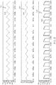
- FIGS. 2 and 3 simulation results for the driver circuit 100 depicted in FIG. 1 and described above are illustrated. These depicted results are for an AC power source 106 that is supplying a single-phase AC voltage of 90-140V RMS (nominal 115VAC) at 400 Hz, and the LED string 122 comprises 16 LEDs connected in series.
- the driver circuit 100 is able to achieve a power factor of 0.99385 with negligible noise in the input current.
- FIG. 2 depicts the input line current (702), the current through the first inductor 112 (704), the current through the second inductor 114 (706), and the current through the LED string 122 (708) over a time-span of 20 milliseconds (msec).
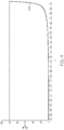
- FIG. 3 depicts the current through the first inductor 112 (704), the current through the second inductor 114 (706), and the current through the LED string 122 (708) over a time-span of 0.13 msec, which more clearly illustrates the pulsed current through the LED string 122.
- the single-stage power factor corrected light emitting diode (LED) driver circuit 100 described herein can be operated in either Buck or Boost modes. Unlike conventional two-stage LED drivers, the inherent Buck-Boost nature of the single-stage power factor corrected light emitting diode (LED) driver circuit 100 disclosed herein does not rely on the use of two switches, nor the associated control circuitry, and allows the input current to be harmonized and the LED current modulated.
- the single-stage power factor corrected light emitting diode (LED) driver circuit 100 disclosed herein also does not include a bulk energy storage capacitor or an output diode. This provides improved response time and transient performance, and improves the reliability of the overall system.
- the single-stage power factor corrected light emitting diode (LED) driver circuit 100 disclosed herein is attractive for low and medium power applications from the perspective of costs, weight, and complexity, and is free from the problems associated with the conventional approaches.
Landscapes
- Engineering & Computer Science (AREA)
- Power Engineering (AREA)
- Circuit Arrangement For Electric Light Sources In General (AREA)
- Led Devices (AREA)
Claims (5)
- Einstufige leistungsfaktorverbesserte Lichtemissionsdioden(LED)-Treiberschaltung (100), die einen Schaltungseingangsknotenpunkt (128), einen Schaltungsausgangsknotenpunkt (102), und einen Schaltungsmasseknotenpunkt (104) aufweist, wobei die Treiberschaltung umfasst:eine erste Induktivität (112);eine zweite Induktivität (114);einen Kopplungskondensator (116);einen steuerbaren Schalter (118), der so ausgeführt ist, dass er selektiv in einem EIN-Zustand, in dem Strom durch den steuerbaren Schalter fließt, und einem AUS-Zustand, in dem kein Strom durch den steuerbaren Schalter fließt, arbeitet;eine LED-Kette (122); undeine Steuerungseinrichtung (138), die mit dem steuerbaren Schalter gekoppelt ist, wobei:die erste Induktivität (112) zwischen dem Schaltungseingangsknotenpunkt (128) und dem Kopplungskondensator (116) elektrisch in Reihe geschaltet ist,die zweite Induktivität (114) zwischen dem Schaltungsausgangsknotenpunkt (102) und dem Schaltungsmasseknotenpunkt (104) elektrisch in Reihe geschaltet ist,der Kopplungskondensator (116) zwischen der ersten Induktivität (112) und dem Schaltungsausgangsknotenpunkt (102) elektrisch in Reihe geschaltet ist,der steuerbare Schalter (118) zwischen einem ersten internen Schaltungsknotenpunkt (134) und dem Schaltungsmasseknotenpunkt (104) elektrisch in Reihe geschaltet ist, wobei der erste interne Schaltungsknotenpunkt (134) zwischen der ersten Induktivität (112) und dem Kopplungskondensator (116) angeordnet ist,dadurch gekennzeichnet, dassdie Steuerungseinrichtung (138) so ausgebildet ist, dass sie ein Referenzspannungssignal (144), das für eine Spannung an dem Schaltungseingangsknotenpunkt (128) charakteristisch ist, und ein LED-Ketten-Stromrückkopplungssignal (142), das für einen Stromfluss durch die LED-Kette charakteristisch ist, empfängt, wobei die Steuerungseinrichtung (138) so ausgeführt ist, dass sie in Reaktion auf das LED-Ketten-Stromrückkopplungssignal (142) und das Referenzspannungssignal (144) dem steuerbaren Schalter (118) befiehlt, selektiv in dem EIN-Zustand und dem AUS-Zustand zu arbeiten,wobei die LED-Kette (122) nur mit der zweiten Induktivität (114) elektrisch parallelgeschaltet ist.
- Treiberschaltung nach Anspruch 1, die ferner umfasst:einen Stromerfassungswiderstand (136), der mit der LED-Kette und der Steuerungseinrichtung gekoppelt ist und so ausgeführt ist, dass er das LED-Ketten-Stromrückkopplungssignal liefert.
- Treiberschaltung nach Anspruch 1, die ferner umfasst:einen Multiplizierer (146), der zwischen dem Schaltungseingangsknotenpunkt und der Steuerungseinrichtung gekoppelt ist und so ausgeführt ist, dass er das Referenzspannungssignal liefert.
- Treiberschaltung nach Anspruch 1, wobei der steuerbare Schalter ein Festkörperschalter ist.
- Treiberschaltung nach Anspruch 4, wobei der Festkörperschalter ein MOSFET ist.
Applications Claiming Priority (1)
| Application Number | Priority Date | Filing Date | Title |
|---|---|---|---|
| US14/830,026 US9763291B2 (en) | 2015-08-19 | 2015-08-19 | Single stage power factor corrected LED driver circuit |
Publications (2)
| Publication Number | Publication Date |
|---|---|
| EP3133902A1 EP3133902A1 (de) | 2017-02-22 |
| EP3133902B1 true EP3133902B1 (de) | 2017-10-11 |
Family
ID=56694030
Family Applications (1)
| Application Number | Title | Priority Date | Filing Date |
|---|---|---|---|
| EP16184403.0A Active EP3133902B1 (de) | 2015-08-19 | 2016-08-16 | Einstufige leistungsfaktorverbesserte led-treiberschaltung |
Country Status (2)
| Country | Link |
|---|---|
| US (1) | US9763291B2 (de) |
| EP (1) | EP3133902B1 (de) |
Families Citing this family (2)
| Publication number | Priority date | Publication date | Assignee | Title |
|---|---|---|---|---|
| RU2643526C2 (ru) * | 2016-05-17 | 2018-02-02 | Юрий Борисович Соколов | Светодиодный источник освещения с питанием от нестабильной трехфазной сети переменного тока |
| KR102306073B1 (ko) * | 2018-07-18 | 2021-09-29 | 이피션트 파워 컨버젼 코퍼레이션 | 집적된 버스 부스트 회로를 갖는 전류 펄스 발생기 |
Family Cites Families (9)
| Publication number | Priority date | Publication date | Assignee | Title |
|---|---|---|---|---|
| US6853150B2 (en) | 2001-12-28 | 2005-02-08 | Koninklijke Philips Electronics N.V. | Light emitting diode driver |
| US7944153B2 (en) | 2006-12-15 | 2011-05-17 | Intersil Americas Inc. | Constant current light emitting diode (LED) driver circuit and method |
| US8228001B2 (en) | 2009-02-24 | 2012-07-24 | Suntec Enterprises | Method and apparatus of driving LED and OLED devices |
| US20110216567A1 (en) | 2010-03-02 | 2011-09-08 | Suntec Enterprises | Single switch inverter |
| US8742676B2 (en) * | 2010-10-29 | 2014-06-03 | Abl Ip Holding Llc | Drive circuit for light emitting diode array based on sepic or cuk topology |
| US8823284B2 (en) * | 2011-11-10 | 2014-09-02 | Honeywell International Inc. | Optimal power supply topologies for switched current-driven LEDs |
| US20140117878A1 (en) | 2012-05-15 | 2014-05-01 | Exar Corporation | Merged-stage high efficiency high power factor hb-led driver without electrolytic capacitor |
| US9554431B2 (en) * | 2014-01-06 | 2017-01-24 | Garrity Power Services Llc | LED driver |
| CN203788519U (zh) | 2014-03-26 | 2014-08-20 | 关侃胜 | 一种led灯驱动电路 |
-
2015
- 2015-08-19 US US14/830,026 patent/US9763291B2/en active Active
-
2016
- 2016-08-16 EP EP16184403.0A patent/EP3133902B1/de active Active
Non-Patent Citations (1)
| Title |
|---|
| None * |
Also Published As
| Publication number | Publication date |
|---|---|
| EP3133902A1 (de) | 2017-02-22 |
| US20170055320A1 (en) | 2017-02-23 |
| US9763291B2 (en) | 2017-09-12 |
Similar Documents
| Publication | Publication Date | Title |
|---|---|---|
| JP4796849B2 (ja) | 直流電源装置、発光ダイオード用電源、及び照明装置 | |
| CN102474189B (zh) | 低成本电源电路和方法 | |
| CN102762015B (zh) | Led控制方法及结构 | |
| US8823284B2 (en) | Optimal power supply topologies for switched current-driven LEDs | |
| JP4975083B2 (ja) | 光源点灯装置および照明装置 | |
| JP6233568B2 (ja) | 電源回路及び照明装置 | |
| JP2010040878A (ja) | 発光ダイオード点灯装置 | |
| CN104349548A (zh) | 点灯装置以及照明器具 | |
| WO2016032579A1 (en) | Floating output voltage boost-buck regulator using a buck controller with low input and low output ripple | |
| JP6283988B2 (ja) | 電源回路及び照明装置 | |
| US9078317B1 (en) | Floating output voltage boost regulator driving LEDs using a buck controller | |
| US9992826B1 (en) | Dual mode constant current LED driver | |
| JP6233567B2 (ja) | 電源回路及び照明装置 | |
| EP3133902B1 (de) | Einstufige leistungsfaktorverbesserte led-treiberschaltung | |
| US20150373805A1 (en) | Light driver and the controller and driving method thereof | |
| JP2010257026A (ja) | 電源回路及び照明装置 | |
| JP2018068117A (ja) | 電源回路及び照明装置 | |
| JP5393744B2 (ja) | Led点灯装置 | |
| JP5150742B2 (ja) | Led駆動回路 | |
| JP6840997B2 (ja) | 照明装置および照明器具 | |
| US10701779B2 (en) | Drive device for illuminating device, illumination device, lighting system and method for controlling the lighting system | |
| WO2012144274A1 (ja) | Led点灯装置およびled照明装置 | |
| Sukanya et al. | A power quality improved isolated bridgeless sepic converter for LED lamp | |
| JP2025071421A (ja) | 点灯装置 | |
| JP2024037451A (ja) | 点灯装置および照明器具 |
Legal Events
| Date | Code | Title | Description |
|---|---|---|---|
| PUAI | Public reference made under article 153(3) epc to a published international application that has entered the european phase |
Free format text: ORIGINAL CODE: 0009012 |
|
| STAA | Information on the status of an ep patent application or granted ep patent |
Free format text: STATUS: REQUEST FOR EXAMINATION WAS MADE |
|
| 17P | Request for examination filed |
Effective date: 20160816 |
|
| AK | Designated contracting states |
Kind code of ref document: A1 Designated state(s): AL AT BE BG CH CY CZ DE DK EE ES FI FR GB GR HR HU IE IS IT LI LT LU LV MC MK MT NL NO PL PT RO RS SE SI SK SM TR |
|
| AX | Request for extension of the european patent |
Extension state: BA ME |
|
| GRAP | Despatch of communication of intention to grant a patent |
Free format text: ORIGINAL CODE: EPIDOSNIGR1 |
|
| STAA | Information on the status of an ep patent application or granted ep patent |
Free format text: STATUS: GRANT OF PATENT IS INTENDED |
|
| RIC1 | Information provided on ipc code assigned before grant |
Ipc: H05B 33/08 20060101AFI20170516BHEP Ipc: H02M 1/42 20070101ALI20170516BHEP |
|
| INTG | Intention to grant announced |
Effective date: 20170601 |
|
| GRAS | Grant fee paid |
Free format text: ORIGINAL CODE: EPIDOSNIGR3 |
|
| GRAA | (expected) grant |
Free format text: ORIGINAL CODE: 0009210 |
|
| STAA | Information on the status of an ep patent application or granted ep patent |
Free format text: STATUS: THE PATENT HAS BEEN GRANTED |
|
| AK | Designated contracting states |
Kind code of ref document: B1 Designated state(s): AL AT BE BG CH CY CZ DE DK EE ES FI FR GB GR HR HU IE IS IT LI LT LU LV MC MK MT NL NO PL PT RO RS SE SI SK SM TR |
|
| REG | Reference to a national code |
Ref country code: GB Ref legal event code: FG4D |
|
| REG | Reference to a national code |
Ref country code: CH Ref legal event code: EP |
|
| REG | Reference to a national code |
Ref country code: IE Ref legal event code: FG4D |
|
| REG | Reference to a national code |
Ref country code: AT Ref legal event code: REF Ref document number: 937109 Country of ref document: AT Kind code of ref document: T Effective date: 20171115 |
|
| REG | Reference to a national code |
Ref country code: DE Ref legal event code: R096 Ref document number: 602016000548 Country of ref document: DE |
|
| REG | Reference to a national code |
Ref country code: NL Ref legal event code: MP Effective date: 20171011 |
|
| REG | Reference to a national code |
Ref country code: LT Ref legal event code: MG4D |
|
| REG | Reference to a national code |
Ref country code: AT Ref legal event code: MK05 Ref document number: 937109 Country of ref document: AT Kind code of ref document: T Effective date: 20171011 |
|
| PG25 | Lapsed in a contracting state [announced via postgrant information from national office to epo] |
Ref country code: NL Free format text: LAPSE BECAUSE OF FAILURE TO SUBMIT A TRANSLATION OF THE DESCRIPTION OR TO PAY THE FEE WITHIN THE PRESCRIBED TIME-LIMIT Effective date: 20171011 |
|
| PG25 | Lapsed in a contracting state [announced via postgrant information from national office to epo] |
Ref country code: FI Free format text: LAPSE BECAUSE OF FAILURE TO SUBMIT A TRANSLATION OF THE DESCRIPTION OR TO PAY THE FEE WITHIN THE PRESCRIBED TIME-LIMIT Effective date: 20171011 Ref country code: ES Free format text: LAPSE BECAUSE OF FAILURE TO SUBMIT A TRANSLATION OF THE DESCRIPTION OR TO PAY THE FEE WITHIN THE PRESCRIBED TIME-LIMIT Effective date: 20171011 Ref country code: LT Free format text: LAPSE BECAUSE OF FAILURE TO SUBMIT A TRANSLATION OF THE DESCRIPTION OR TO PAY THE FEE WITHIN THE PRESCRIBED TIME-LIMIT Effective date: 20171011 Ref country code: SE Free format text: LAPSE BECAUSE OF FAILURE TO SUBMIT A TRANSLATION OF THE DESCRIPTION OR TO PAY THE FEE WITHIN THE PRESCRIBED TIME-LIMIT Effective date: 20171011 Ref country code: NO Free format text: LAPSE BECAUSE OF FAILURE TO SUBMIT A TRANSLATION OF THE DESCRIPTION OR TO PAY THE FEE WITHIN THE PRESCRIBED TIME-LIMIT Effective date: 20180111 |
|
| PG25 | Lapsed in a contracting state [announced via postgrant information from national office to epo] |
Ref country code: RS Free format text: LAPSE BECAUSE OF FAILURE TO SUBMIT A TRANSLATION OF THE DESCRIPTION OR TO PAY THE FEE WITHIN THE PRESCRIBED TIME-LIMIT Effective date: 20171011 Ref country code: BG Free format text: LAPSE BECAUSE OF FAILURE TO SUBMIT A TRANSLATION OF THE DESCRIPTION OR TO PAY THE FEE WITHIN THE PRESCRIBED TIME-LIMIT Effective date: 20180111 Ref country code: GR Free format text: LAPSE BECAUSE OF FAILURE TO SUBMIT A TRANSLATION OF THE DESCRIPTION OR TO PAY THE FEE WITHIN THE PRESCRIBED TIME-LIMIT Effective date: 20180112 Ref country code: HR Free format text: LAPSE BECAUSE OF FAILURE TO SUBMIT A TRANSLATION OF THE DESCRIPTION OR TO PAY THE FEE WITHIN THE PRESCRIBED TIME-LIMIT Effective date: 20171011 Ref country code: IS Free format text: LAPSE BECAUSE OF FAILURE TO SUBMIT A TRANSLATION OF THE DESCRIPTION OR TO PAY THE FEE WITHIN THE PRESCRIBED TIME-LIMIT Effective date: 20180211 Ref country code: LV Free format text: LAPSE BECAUSE OF FAILURE TO SUBMIT A TRANSLATION OF THE DESCRIPTION OR TO PAY THE FEE WITHIN THE PRESCRIBED TIME-LIMIT Effective date: 20171011 Ref country code: AT Free format text: LAPSE BECAUSE OF FAILURE TO SUBMIT A TRANSLATION OF THE DESCRIPTION OR TO PAY THE FEE WITHIN THE PRESCRIBED TIME-LIMIT Effective date: 20171011 |
|
| REG | Reference to a national code |
Ref country code: DE Ref legal event code: R097 Ref document number: 602016000548 Country of ref document: DE |
|
| PG25 | Lapsed in a contracting state [announced via postgrant information from national office to epo] |
Ref country code: EE Free format text: LAPSE BECAUSE OF FAILURE TO SUBMIT A TRANSLATION OF THE DESCRIPTION OR TO PAY THE FEE WITHIN THE PRESCRIBED TIME-LIMIT Effective date: 20171011 Ref country code: DK Free format text: LAPSE BECAUSE OF FAILURE TO SUBMIT A TRANSLATION OF THE DESCRIPTION OR TO PAY THE FEE WITHIN THE PRESCRIBED TIME-LIMIT Effective date: 20171011 Ref country code: SK Free format text: LAPSE BECAUSE OF FAILURE TO SUBMIT A TRANSLATION OF THE DESCRIPTION OR TO PAY THE FEE WITHIN THE PRESCRIBED TIME-LIMIT Effective date: 20171011 Ref country code: CZ Free format text: LAPSE BECAUSE OF FAILURE TO SUBMIT A TRANSLATION OF THE DESCRIPTION OR TO PAY THE FEE WITHIN THE PRESCRIBED TIME-LIMIT Effective date: 20171011 |
|
| PLBE | No opposition filed within time limit |
Free format text: ORIGINAL CODE: 0009261 |
|
| STAA | Information on the status of an ep patent application or granted ep patent |
Free format text: STATUS: NO OPPOSITION FILED WITHIN TIME LIMIT |
|
| PG25 | Lapsed in a contracting state [announced via postgrant information from national office to epo] |
Ref country code: PL Free format text: LAPSE BECAUSE OF FAILURE TO SUBMIT A TRANSLATION OF THE DESCRIPTION OR TO PAY THE FEE WITHIN THE PRESCRIBED TIME-LIMIT Effective date: 20171011 Ref country code: SM Free format text: LAPSE BECAUSE OF FAILURE TO SUBMIT A TRANSLATION OF THE DESCRIPTION OR TO PAY THE FEE WITHIN THE PRESCRIBED TIME-LIMIT Effective date: 20171011 Ref country code: IT Free format text: LAPSE BECAUSE OF FAILURE TO SUBMIT A TRANSLATION OF THE DESCRIPTION OR TO PAY THE FEE WITHIN THE PRESCRIBED TIME-LIMIT Effective date: 20171011 |
|
| 26N | No opposition filed |
Effective date: 20180712 |
|
| PG25 | Lapsed in a contracting state [announced via postgrant information from national office to epo] |
Ref country code: MC Free format text: LAPSE BECAUSE OF FAILURE TO SUBMIT A TRANSLATION OF THE DESCRIPTION OR TO PAY THE FEE WITHIN THE PRESCRIBED TIME-LIMIT Effective date: 20171011 |
|
| PG25 | Lapsed in a contracting state [announced via postgrant information from national office to epo] |
Ref country code: LU Free format text: LAPSE BECAUSE OF NON-PAYMENT OF DUE FEES Effective date: 20180816 |
|
| REG | Reference to a national code |
Ref country code: BE Ref legal event code: MM Effective date: 20180831 |
|
| REG | Reference to a national code |
Ref country code: IE Ref legal event code: MM4A |
|
| PG25 | Lapsed in a contracting state [announced via postgrant information from national office to epo] |
Ref country code: IE Free format text: LAPSE BECAUSE OF NON-PAYMENT OF DUE FEES Effective date: 20180816 |
|
| PG25 | Lapsed in a contracting state [announced via postgrant information from national office to epo] |
Ref country code: FR Free format text: LAPSE BECAUSE OF NON-PAYMENT OF DUE FEES Effective date: 20180831 Ref country code: BE Free format text: LAPSE BECAUSE OF NON-PAYMENT OF DUE FEES Effective date: 20180831 |
|
| REG | Reference to a national code |
Ref country code: DE Ref legal event code: R079 Ref document number: 602016000548 Country of ref document: DE Free format text: PREVIOUS MAIN CLASS: H05B0033080000 Ipc: H05B0045000000 |
|
| PG25 | Lapsed in a contracting state [announced via postgrant information from national office to epo] |
Ref country code: MT Free format text: LAPSE BECAUSE OF NON-PAYMENT OF DUE FEES Effective date: 20180816 |
|
| PG25 | Lapsed in a contracting state [announced via postgrant information from national office to epo] |
Ref country code: TR Free format text: LAPSE BECAUSE OF FAILURE TO SUBMIT A TRANSLATION OF THE DESCRIPTION OR TO PAY THE FEE WITHIN THE PRESCRIBED TIME-LIMIT Effective date: 20171011 |
|
| PG25 | Lapsed in a contracting state [announced via postgrant information from national office to epo] |
Ref country code: CH Free format text: LAPSE BECAUSE OF NON-PAYMENT OF DUE FEES Effective date: 20190831 Ref country code: LI Free format text: LAPSE BECAUSE OF NON-PAYMENT OF DUE FEES Effective date: 20190831 Ref country code: PT Free format text: LAPSE BECAUSE OF FAILURE TO SUBMIT A TRANSLATION OF THE DESCRIPTION OR TO PAY THE FEE WITHIN THE PRESCRIBED TIME-LIMIT Effective date: 20171011 |
|
| PG25 | Lapsed in a contracting state [announced via postgrant information from national office to epo] |
Ref country code: CY Free format text: LAPSE BECAUSE OF FAILURE TO SUBMIT A TRANSLATION OF THE DESCRIPTION OR TO PAY THE FEE WITHIN THE PRESCRIBED TIME-LIMIT Effective date: 20171011 Ref country code: HU Free format text: LAPSE BECAUSE OF FAILURE TO SUBMIT A TRANSLATION OF THE DESCRIPTION OR TO PAY THE FEE WITHIN THE PRESCRIBED TIME-LIMIT; INVALID AB INITIO Effective date: 20160816 Ref country code: MK Free format text: LAPSE BECAUSE OF NON-PAYMENT OF DUE FEES Effective date: 20171011 Ref country code: RO Free format text: LAPSE BECAUSE OF FAILURE TO SUBMIT A TRANSLATION OF THE DESCRIPTION OR TO PAY THE FEE WITHIN THE PRESCRIBED TIME-LIMIT Effective date: 20171011 |
|
| PG25 | Lapsed in a contracting state [announced via postgrant information from national office to epo] |
Ref country code: AL Free format text: LAPSE BECAUSE OF FAILURE TO SUBMIT A TRANSLATION OF THE DESCRIPTION OR TO PAY THE FEE WITHIN THE PRESCRIBED TIME-LIMIT Effective date: 20171011 |
|
| PG25 | Lapsed in a contracting state [announced via postgrant information from national office to epo] |
Ref country code: SI Free format text: LAPSE BECAUSE OF NON-PAYMENT OF DUE FEES Effective date: 20180816 |
|
| GBPC | Gb: european patent ceased through non-payment of renewal fee |
Effective date: 20200816 |
|
| PG25 | Lapsed in a contracting state [announced via postgrant information from national office to epo] |
Ref country code: GB Free format text: LAPSE BECAUSE OF NON-PAYMENT OF DUE FEES Effective date: 20200816 |
|
| P01 | Opt-out of the competence of the unified patent court (upc) registered |
Effective date: 20230525 |
|
| PGFP | Annual fee paid to national office [announced via postgrant information from national office to epo] |
Ref country code: DE Payment date: 20250827 Year of fee payment: 10 |