EP3133333B1 - Dispositif électroluminescent et dispositif d'affichage - Google Patents
Dispositif électroluminescent et dispositif d'affichage Download PDFInfo
- Publication number
- EP3133333B1 EP3133333B1 EP15764759.5A EP15764759A EP3133333B1 EP 3133333 B1 EP3133333 B1 EP 3133333B1 EP 15764759 A EP15764759 A EP 15764759A EP 3133333 B1 EP3133333 B1 EP 3133333B1
- Authority
- EP
- European Patent Office
- Prior art keywords
- light
- guiding plate
- light sources
- sources
- incidence surface
- Prior art date
- Legal status (The legal status is an assumption and is not a legal conclusion. Google has not performed a legal analysis and makes no representation as to the accuracy of the status listed.)
- Active
Links
- 230000003287 optical effect Effects 0.000 claims description 26
- 238000006243 chemical reaction Methods 0.000 claims description 10
- 238000009792 diffusion process Methods 0.000 claims description 5
- 239000000463 material Substances 0.000 claims description 5
- 230000010287 polarization Effects 0.000 claims description 3
- 238000000926 separation method Methods 0.000 claims description 2
- 238000009826 distribution Methods 0.000 description 64
- 230000000052 comparative effect Effects 0.000 description 29
- 238000010586 diagram Methods 0.000 description 17
- 239000011295 pitch Substances 0.000 description 14
- 230000000694 effects Effects 0.000 description 8
- 239000004973 liquid crystal related substance Substances 0.000 description 6
- 229920000139 polyethylene terephthalate Polymers 0.000 description 5
- 239000005020 polyethylene terephthalate Substances 0.000 description 5
- 239000011347 resin Substances 0.000 description 5
- 229920005989 resin Polymers 0.000 description 5
- 229920003229 poly(methyl methacrylate) Polymers 0.000 description 4
- 229920005668 polycarbonate resin Polymers 0.000 description 3
- 239000004431 polycarbonate resin Substances 0.000 description 3
- 239000004926 polymethyl methacrylate Substances 0.000 description 3
- 239000004925 Acrylic resin Substances 0.000 description 2
- 229920000178 Acrylic resin Polymers 0.000 description 2
- PPBRXRYQALVLMV-UHFFFAOYSA-N Styrene Chemical compound C=CC1=CC=CC=C1 PPBRXRYQALVLMV-UHFFFAOYSA-N 0.000 description 2
- 229920001577 copolymer Polymers 0.000 description 2
- 230000003247 decreasing effect Effects 0.000 description 2
- 238000001704 evaporation Methods 0.000 description 2
- 230000008020 evaporation Effects 0.000 description 2
- 239000000203 mixture Substances 0.000 description 2
- 229920001225 polyester resin Polymers 0.000 description 2
- 239000004645 polyester resin Substances 0.000 description 2
- -1 polyethylene terephthalate Polymers 0.000 description 2
- 229920005992 thermoplastic resin Polymers 0.000 description 2
- VVQNEPGJFQJSBK-UHFFFAOYSA-N Methyl methacrylate Chemical compound COC(=O)C(C)=C VVQNEPGJFQJSBK-UHFFFAOYSA-N 0.000 description 1
- BQCADISMDOOEFD-UHFFFAOYSA-N Silver Chemical compound [Ag] BQCADISMDOOEFD-UHFFFAOYSA-N 0.000 description 1
- XAGFODPZIPBFFR-UHFFFAOYSA-N aluminium Chemical compound [Al] XAGFODPZIPBFFR-UHFFFAOYSA-N 0.000 description 1
- 229910052782 aluminium Inorganic materials 0.000 description 1
- 230000006866 deterioration Effects 0.000 description 1
- 238000005516 engineering process Methods 0.000 description 1
- 230000002708 enhancing effect Effects 0.000 description 1
- 238000001125 extrusion Methods 0.000 description 1
- 230000014509 gene expression Effects 0.000 description 1
- 239000011521 glass Substances 0.000 description 1
- 238000005286 illumination Methods 0.000 description 1
- 238000003754 machining Methods 0.000 description 1
- 238000004519 manufacturing process Methods 0.000 description 1
- 238000000034 method Methods 0.000 description 1
- 238000012986 modification Methods 0.000 description 1
- 230000004048 modification Effects 0.000 description 1
- 238000000465 moulding Methods 0.000 description 1
- 230000001151 other effect Effects 0.000 description 1
- 229920005990 polystyrene resin Polymers 0.000 description 1
- 239000004800 polyvinyl chloride Substances 0.000 description 1
- 229920000915 polyvinyl chloride Polymers 0.000 description 1
- 239000004065 semiconductor Substances 0.000 description 1
- 229910052709 silver Inorganic materials 0.000 description 1
- 239000004332 silver Substances 0.000 description 1
- 229920006352 transparent thermoplastic Polymers 0.000 description 1
Images


Classifications
-
- G—PHYSICS
- G02—OPTICS
- G02B—OPTICAL ELEMENTS, SYSTEMS OR APPARATUS
- G02B6/00—Light guides; Structural details of arrangements comprising light guides and other optical elements, e.g. couplings
- G02B6/0001—Light guides; Structural details of arrangements comprising light guides and other optical elements, e.g. couplings specially adapted for lighting devices or systems
- G02B6/0011—Light guides; Structural details of arrangements comprising light guides and other optical elements, e.g. couplings specially adapted for lighting devices or systems the light guides being planar or of plate-like form
- G02B6/0033—Means for improving the coupling-out of light from the light guide
- G02B6/0035—Means for improving the coupling-out of light from the light guide provided on the surface of the light guide or in the bulk of it
- G02B6/004—Scattering dots or dot-like elements, e.g. microbeads, scattering particles, nanoparticles
- G02B6/0043—Scattering dots or dot-like elements, e.g. microbeads, scattering particles, nanoparticles provided on the surface of the light guide
-
- G—PHYSICS
- G02—OPTICS
- G02B—OPTICAL ELEMENTS, SYSTEMS OR APPARATUS
- G02B6/00—Light guides; Structural details of arrangements comprising light guides and other optical elements, e.g. couplings
- G02B6/0001—Light guides; Structural details of arrangements comprising light guides and other optical elements, e.g. couplings specially adapted for lighting devices or systems
- G02B6/0011—Light guides; Structural details of arrangements comprising light guides and other optical elements, e.g. couplings specially adapted for lighting devices or systems the light guides being planar or of plate-like form
- G02B6/0033—Means for improving the coupling-out of light from the light guide
- G02B6/005—Means for improving the coupling-out of light from the light guide provided by one optical element, or plurality thereof, placed on the light output side of the light guide
-
- G—PHYSICS
- G02—OPTICS
- G02B—OPTICAL ELEMENTS, SYSTEMS OR APPARATUS
- G02B6/00—Light guides; Structural details of arrangements comprising light guides and other optical elements, e.g. couplings
- G02B6/0001—Light guides; Structural details of arrangements comprising light guides and other optical elements, e.g. couplings specially adapted for lighting devices or systems
- G02B6/0011—Light guides; Structural details of arrangements comprising light guides and other optical elements, e.g. couplings specially adapted for lighting devices or systems the light guides being planar or of plate-like form
- G02B6/0033—Means for improving the coupling-out of light from the light guide
- G02B6/0058—Means for improving the coupling-out of light from the light guide varying in density, size, shape or depth along the light guide
- G02B6/0061—Means for improving the coupling-out of light from the light guide varying in density, size, shape or depth along the light guide to provide homogeneous light output intensity
-
- G—PHYSICS
- G02—OPTICS
- G02B—OPTICAL ELEMENTS, SYSTEMS OR APPARATUS
- G02B6/00—Light guides; Structural details of arrangements comprising light guides and other optical elements, e.g. couplings
- G02B6/0001—Light guides; Structural details of arrangements comprising light guides and other optical elements, e.g. couplings specially adapted for lighting devices or systems
- G02B6/0011—Light guides; Structural details of arrangements comprising light guides and other optical elements, e.g. couplings specially adapted for lighting devices or systems the light guides being planar or of plate-like form
- G02B6/0066—Light guides; Structural details of arrangements comprising light guides and other optical elements, e.g. couplings specially adapted for lighting devices or systems the light guides being planar or of plate-like form characterised by the light source being coupled to the light guide
- G02B6/0068—Arrangements of plural sources, e.g. multi-colour light sources
-
- G—PHYSICS
- G02—OPTICS
- G02B—OPTICAL ELEMENTS, SYSTEMS OR APPARATUS
- G02B6/00—Light guides; Structural details of arrangements comprising light guides and other optical elements, e.g. couplings
- G02B6/0001—Light guides; Structural details of arrangements comprising light guides and other optical elements, e.g. couplings specially adapted for lighting devices or systems
- G02B6/0011—Light guides; Structural details of arrangements comprising light guides and other optical elements, e.g. couplings specially adapted for lighting devices or systems the light guides being planar or of plate-like form
- G02B6/0066—Light guides; Structural details of arrangements comprising light guides and other optical elements, e.g. couplings specially adapted for lighting devices or systems the light guides being planar or of plate-like form characterised by the light source being coupled to the light guide
- G02B6/0073—Light emitting diode [LED]
-
- G—PHYSICS
- G02—OPTICS
- G02B—OPTICAL ELEMENTS, SYSTEMS OR APPARATUS
- G02B6/00—Light guides; Structural details of arrangements comprising light guides and other optical elements, e.g. couplings
- G02B6/0001—Light guides; Structural details of arrangements comprising light guides and other optical elements, e.g. couplings specially adapted for lighting devices or systems
- G02B6/0011—Light guides; Structural details of arrangements comprising light guides and other optical elements, e.g. couplings specially adapted for lighting devices or systems the light guides being planar or of plate-like form
- G02B6/0075—Arrangements of multiple light guides
- G02B6/0076—Stacked arrangements of multiple light guides of the same or different cross-sectional area
Definitions
- the present disclosure relates to a light-emitting device, and a display device equipped with it.
- a backlight for liquid crystal display devices and the like light-emitting devices performing surface emission of light outgoing from a light source utilizing light-guiding plates are known.
- a structure is known that disposes a plurality of punctiform light sources such as LEDs (Light-Emitting Diodes) and laser diodes on side faces of light-guiding plates.
- PTL 3 discloses a planar illumination apparatus having diffuse reflection patterns formed on light guide plates for diffusing and reflecting light that enters the same.
- PTL 4 discloses a backlight module including a first light guide plate and a second light guide plate.
- the first light guide plate includes a first bottom surface and plurality of reflective micro-structures formed at the first bottom surface.
- the second light guide plate is located adjacent the first bottom surface of the first light guide plate.
- the second light guide plate includes a second bottom surface, and plurality of diffusing micro-structures formed at the second bottom surface.
- PTL5 discloses a liquid crystal flat panel display monitor having a wide aspect ratio.
- PTL6 discloses a light emitting device and display device using the same.
- PTL7 discloses a lighting system and back-light device using this lighting system.
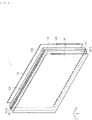
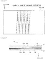
- FIG. 1 illustrates an overall configuration of a light-emitting device (backlight unit 1) according to a first aspect of the present disclosure.
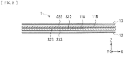
- FIG. 2 illustrates a cross-sectional configuration of the backlight unit 1.
- the backlight unit 1 may illuminate a transmissive liquid crystal panel from behind, and has first light sources 10-1, second light sources 10-2, a lower light-guiding plate 11A, an upper light-guiding plate 11B, a reflective sheet 12, and an optical sheet 13.
- the "lower light-guiding plate 11A” corresponds to a specific example of a “first light-guiding plate” in one aspect.
- the "upper light-guiding plate 11B” corresponds to a specific example of a “second light-guiding plate” in one aspect.
- Each of the first light sources 10-1 and the second light sources 10-2 is a punctiform light source, and more specifically, includes a laser diode (semiconductor laser).
- a laser diode semiconductor laser
- a laser diode that emits, for example, red-color, green-color, or blue-color light may be used.
- a plurality of first light sources 10-1 are so provided side by side as to face a light incidence surface (first light incidence surface) of the lower light-guiding plate 11A.
- a plurality of second light sources 10-2 are so provided side by side as to face a light incidence surface (second light incidence surface) of the upper light-guiding plate 11B.
- first light sources 10-1 and the second light sources 10-2 may be LEDs (Light-Emitting Diodes), or laser diodes and light-emitting diodes may be mixed in the plurality of first light sources 10-1 and the plurality of second light sources 10-2.
- LEDs Light-Emitting Diodes
- laser diodes and light-emitting diodes may be mixed in the plurality of first light sources 10-1 and the plurality of second light sources 10-2.
- Both the lower light-guiding plate 11A and the upper light-guiding plate 11B may be, for example, tabular (flat and rectangular parallelepiped) optical members.
- the lower light-guiding plate 11A has the first light incidence surface and a first light emitting surface, and is intended to guide light incoming from the first light incidence surface to the first light emitting surface.
- the upper light-guiding plate 11B has the second light incidence surface and a second light emitting surface, and is intended to guide light incoming from the second light incidence surface to the second light emitting surface.
- the lower light-guiding plate 11A has a first light emission enhancement surface on which a first dot pattern 30-1 to be hereinafter described is provided.
- the upper light-guiding plate 11B has a second light emission enhancement surface on which a second dot pattern 30-2 to be hereinafter described is provided.
- Each of the lower light-guiding plate 11A and the upper light-guiding plate 11B may be configured to mainly contain a transparent thermoplastic resin material, such as polycarbonate resin (PC) or acrylic resin (for example, PMMA (polymethylmethacrylate)).
- the lower light-guiding plate 11A and the upper light-guiding plate 11B may face each other along Z direction, for example, in such a manner that superposed emitting light for each of the lower light-guiding plate 11A and the upper light-guiding plate 11B forms a light-emitting luminance distribution in the backlight unit 1. From the first light emitting surface and the second light emitting surface, light is emitted toward the Z direction as a predetermined light emission direction.
- the reflective sheet 12 is a tabular or planar member that is configured to to face the backside of the lower light-guiding plate 11A (a second main surface S13 facing the second light emitting surface), and is intended to return light leaking out of the lower light-guiding plate 11A (or the upper light-guiding plate 11B) toward the lower light-guiding plate 11A.
- the reflective sheet 12 has functions such as reflection, diffusion, and scattering, which makes it possible to efficiently utilize light from the first light sources 10-1 and the second light sources 10-2, thereby enhancing the frontal luminance.
- This reflective sheet 12 may be constituted by, for example, expanded PET (polyethylene terephthalate), silver-evaporated film, multi-layer reflective film, or white PET.
- expanded PET polyethylene terephthalate
- silver-evaporated film multi-layer reflective film
- white PET white PET
- the surface of the reflective sheet 12 be subjected to a treatment such as silver evaporation, aluminum evaporation, or multi-layer film reflection.
- the reflective sheet 12 When the reflective sheet 12 is given a microscopic geometry, the reflective sheet 12 may be formed in an integrated manner by use of a method such as thermal press molding utilizing thermoplastic resin or melt extrusion molding, or may be formed in such a manner that a base material made of, for example, PET is coated with energy ray (for example, ultraviolet) curable resin, and thereafter a shape is transferred onto the energy ray curable resin.
- a method such as thermal press molding utilizing thermoplastic resin or melt extrusion molding
- thermoplastic resin may include polycarbonate resin, acrylic resin such as PMMA (polymethylmethacrylate), polyester resin such as polyethylene terephthalate, amorphous copolymer polyester resin such as MS (copolymer of methyl methacrylate and styrene), polystyrene resin, and polyvinyl chloride resin.
- a base material may be made of glass.
- the optical sheet 13 is configured to to face the first light emitting surface of the upper light-guiding plate 11B, and may include, for example, a diffusion plate, a diffusion sheet, a lens film, and a polarization separation sheet. By providing such an optical sheet 13, it is possible to make light outgoing in an oblique direction from the upper light-guiding plate 11B rise toward a front direction, which allows the frontal luminance to be further enhanced.
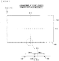
- FIG. 3 illustrates an arrangement configuration of the lower light-guiding plate 11A, the upper light-guiding plate 11B, the first light sources 10-1, and the second light sources 10-2 in X-Y plane.
- the lower light-guiding plate 11A has a first main surface S12 and a second main surface S13.
- the upper light-guiding plate 11B has a first main surface S22 and a second main surface S23.
- one side face (a first side face S1) is the first light incidence surface, while one main surface S12 (a surface facing the upper light-guiding plate 11B) is the first light emitting surface. Further, another main surface S13 is a first light emission enhancement surface on which a first dot pattern 30-1 is provided.
- one side face constitutes the second light incidence surface
- one main surface S22 (a surface facing the optical sheet 13) constitutes the second light emitting surface.
- the light emitting surface of the upper light-guiding plate 11B configures a light output surface of an entire light-guiding section.
- another main surface S23 is a second light emission enhancement surface on which a second dot pattern 30-2 is provided.
- the lower light-guiding plate 11A and the upper light-guiding plate 11B are stacked in such a manner that the first light incidence surface and the second light incidence surface are not superposed on each other in Z direction.
- the first light incidence surface of the lower light-guiding plate 11A is provided on either one (for example, the first side face S1) of two side face corresponding to long sides of an X-Y planar shape (for example, a rectangular shape), and the second light incidence surface of the upper light-guiding plate 11B is provided on the other surface (for example, the second side face S2) of two side face corresponding to long sides of the rectangular shape.
- the plurality of first light sources 10-1 are arranged to face the first light incidence surface of the lower light-guiding plate 11A along one direction.
- the plurality of second light sources 10-2 are arranged to face the second light incidence surface of the upper light-guiding plate 11B along one direction.
- a light emission direction Z direction
- light is emitted toward directions opposite to each other from the first light sources 10-1 and the second light sources 10-2, and light moving toward directions opposite to each other enters on the lower light-guiding plate 11A and the upper light-guiding plate 11B.
- the first dot pattern 30-1 is provided to cover a region making up more than half of the first light emission enhancement surface of the lower light-guiding plate 11A.
- the second dot pattern 30-2 is provided to cover a region making up more than half of the second light emission enhancement surface of the upper light-guiding plate 11B. As illustrated in FIG. 3 , this ensures to have an overlapping region in which regions provided with the first dot pattern 30-1 and the second dot pattern 30-2 partially overlap when viewed from a light emission direction.
- FIG. 4 schematically illustrates the second dot pattern 30-2 of the upper light-guiding plate 11B, and the first dot pattern 30-1 of the lower light-guiding plate 11A also has a substantially similar configuration with the exception that a direction where a pattern density becomes higher is opposite.
- the lower light-guiding plate 11A has the first dot pattern 30-1 configured in such a manner that microscopic dots 31 are provided as first punctiform sections on the first light emission enhancement surface.
- the upper light-guiding plate 11B also has a substantially similar configuration, and has the second dot pattern 30-2 configured in such a manner that the dots 31 are provided as second punctiform sections on the second light emission enhancement surface.
- Each of the first dot pattern 30-1 and the second dot pattern 30-2 is formed of a white dot pattern that is silkscreen-printed using a white ink, for example.
- a pattern having convex or concave portions corresponding to the dots 31 may be formed using laser machining, for example.
- the lower light-guiding plate 11A is configured in such a manner that the density of the dots 31 in the first dot pattern 30-1 changes depending on distance from the light incidence surface.
- the upper light-guiding plate 11B is also configured in such a manner that the density of the dots 31 in the second dot pattern 30-2 changes depending on distance from the light incidence surface. More specifically, in the lower light-guiding plate 11A, the density of the dots 31 becomes higher with increasing distance from the light incidence surface (the density of the dots 31 becomes lower with decreasing distance from the light incidence surface). Also in the upper light-guiding plate 11B, the density of the dots 31 becomes higher with increasing distance from the light incidence surface (the density of the dots 31 becomes lower with decreasing distance from the light incidence surface). As a result, as illustrated in FIG.
- the dot density is allowed to be changed in a step-by-step manner by changing, for example, but not limited to, the number, pitch, and size of the dots 31 for each region.
- the density of each of the first dot pattern 30-1 and the second dot pattern 30-2 be changed by changing both the arrangement pitch (dot pitch) and the size (dot size) of the dots 31.
- a dot size Ds1 in a portion with the relatively lower density smaller than a dot size Ds2 in a portion with the relatively higher density.
- a dot pitch Xp2 in X direction and a dot pitch Yp2 in Y direction in a portion with the relatively higher density smaller than a dot pitch Xp1 in X direction and a dot pitch Yp1 in Y direction in a portion with the relatively lower density.
- FIG. 5 illustrates a first example of arrangement of the light sources 10.
- Each of the first light sources 10-1 and the second light sources 10-2 may include a red light source 10R that emits red-color light, a green light source 10G that emits blue-color light, and a blue light source 10B that emits green-color light.
- White-color light may be generated by color mixture of such color light.
- each of the first light sources 10-1 and the second light sources 10-2 may configure a single light source unit 10U using a predetermined number of color light sources.
- three red light sources 10R, one green light source 10G, and one blue light source 10B configure the single light source unit 10U.
- FIG. 5 illustrates a first example of arrangement of the light sources 10.
- Each of the first light sources 10-1 and the second light sources 10-2 may include a red light source 10R that emits red-color light, a green light source 10G that emits blue-color light, and a blue light source 10B that emits green-color light.
- optical axis positions of the respective first light sources 10-1 are the same as optical axis positions of the respective second light sources 10-2. More specifically, the optical axis positions of respective light sources in X direction in the lower light-guiding plate 11A are the same as the optical axis positions of respective light sources in X direction in the upper light-guiding plate 11B.
- FIG. 6 illustrates a second example of arrangement of the light sources 10.
- relative positions of the first light sources 10-1 and the second light sources 10-2 may be offset in such a manner that the optical axis positions of the first light sources 10-1 and the second light sources 10-2 in X direction are different from each other.
- the optical axis positions of the first light sources 10-1 in one of the light source units 10U and the second light sources 10-2 in a corresponding light source unit 10U are different from each other.
- the light that has been emitted from the first light sources 10-1 and has entered the light incidence surface of the lower light-guiding plate 11A proceeds through the lower light-guiding plate 11A to exit from the first light emitting surface.
- the light that has been emitted from the second light sources 10-2 and has entered the second light incidence surface of the upper light-guiding plate 11B proceeds through the upper light-guiding plate 11B to exit from the second light emitting surface.
- the light outgoing from each of the lower light-guiding plate 11A and the light from upper light-guiding plate 11B are combined, and the resulting light passes through the optical sheet 13 to be observed as emitted light.
- a dot pattern optimized to reduce luminance unevenness or color unevenness is provided on each of two light-guiding plates that face each other, and thus it is possible to reduce the luminance unevenness or color unevenness. Further, by optimizing the arrangement of respective light sources that face the light incidence surfaces of respective light-guiding plates, it is possible to further reduce the luminance unevenness or color unevenness.
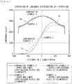
- FIG. 7 compares coverage of dot patterns in a comparative example 1 and an example 1 of aspect.
- FIG. 7 illustrates coverage of the second dot pattern 30-2 in the upper light-guiding plate 11B; however, coverage of the first dot pattern 30-1 in the lower light-guiding plate 11A may be also substantially similar to the above coverage.
- a vertical scale denotes coverage of the second dot pattern 30-2
- a horizontal scale denotes a distance in Y direction.
- the distance in Y direction defines a center of Y direction as 0, and a light incidence surface side (a side on which the light sources are disposed) as a minus direction. This is applicable to other subsequent characteristic diagrams.
- the second light incidence surface side (a side on which the second light sources 10-2 are disposed) is defined as a minus direction.
- the first light incidence surface side (a side on which the first light sources 10-1 are disposed) is defined as a minus direction.
- the dot patterns 30-1 and 30-2 are provided only from the center of Y direction toward a plus direction in the comparative example 1.
- the first dot pattern 30-1 is provided to cover a region making up more than half of the first light emission enhancement surface of the lower light-guiding plate 11A
- the second dot pattern 30-2 is provided to cover a region making up more than half of the second light emission enhancement surface of the upper light-guiding plate 11B.
- the comparative example 1 illustrates a configuration where overlapping regions of the dot patterns 30-1 and 30-2 (see FIG. 3 ) are not provided.
- the dot patterns 30-1 and 30-2 are also provided at a minus side of Y direction, and overlapping regions of the dot patterns 30-1 and 30-2 (see FIG. 3 ) are provided.
- FIG. 8 illustrates dimensions of each section of the upper light-guiding plate 11B in the comparative example 1 and the example 1 of aspect.
- FIG. 9 illustrates dimensions of each section of the lower light-guiding plate 11A in the comparative example 1 and the example 1 of aspect.
- FIG. 9 also illustrates dimensions in arrangement of the first light sources 10-1; however, dimensions in arrangement of the second light sources 10-2 are also basically similar to the above dimensions.
- optical axis positions of the first light sources 10-1 and the second light sources 10-2 in X direction are the same to each other. It is to be noted that also in a comparative example 2 to be hereinafter described, the dimensions are similar to those illustrated in FIG. 8 and FIG. 9 .
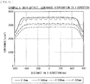
- FIG. 10 compares luminance distributions in Y direction in the comparative example 1 and the example 1 of aspect.
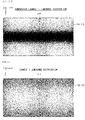
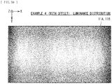
- FIG. 11 illustrates an in-plane luminance distribution in the comparative example 1.
- FIG. 12 illustrates an in-plane luminance distribution in the example 1 of aspect.
- a vertical scale denotes luminance
- a horizontal scale denotes a distance in Y direction.
- FIG. 10 illustrates characteristics in a case where both the lower light-guiding plate 11A and the upper light-guiding plate 11B are illuminated and characteristics in a case where only the upper light-guiding plate 11B is illuminated.
- FIG. 13 compares coverage of dot patterns in the comparative example 2 and the example 1 of aspect.
- FIG. 13 illustrates coverage of the second dot pattern 30-2 in the upper light-guiding plate 11B; however, coverage of the first dot pattern 30-1 in the lower light-guiding plate 11A may be also substantially similar to the above coverage.
- a vertical scale denotes coverage of the second dot pattern 30-2, and a horizontal scale denotes a distance in Y direction.
- FIG. 14 illustrates a configuration of the second dot pattern 30-2 of the upper light-guiding plate 11B in the comparative example 2; however, a configuration of the first dot pattern 30-1 of the lower light-guiding plate 11A may be also substantially similar to the above configuration.
- FIG. 15 illustrates a configuration of the second dot pattern 30-2 of the upper light-guiding plate 11B in the example 1 of aspect; however, a configuration of the first dot pattern 30-1 of the lower light-guiding plate 11A may be also substantially similar to the above configuration. It is to be noted that FIG. 15 illustrates, for reference, a boundary 40 of a valid region available as illuminating light.
- the pattern density in the second dot pattern 30-2 of the upper light-guiding plate 11B (and the first dot pattern 30-1 of the lower light-guiding plate 11A) is changed by changing a dot pitch (and a dot size) of the dots 31 according to position in Y direction.
- the pattern density in the comparative example 1 is changed only by changing a dot size without changing a dot pitch.
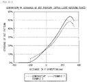
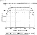
- FIG. 16 compares luminance distributions in Y direction in the comparative example 2 and the example 1 of aspect.
- FIG. 17 illustrates the in-plane luminance distribution in the comparative example 2.
- a vertical scale denotes luminance
- a horizontal scale denotes a distance in Y direction.
- FIG. 16 illustrates characteristics in a case where both the lower light-guiding plate 11A and the upper light-guiding plate 11B are illuminated and characteristics in a case where only the upper light-guiding plate 11B is illuminated.
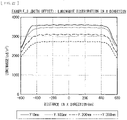
- FIG. 18 illustrates a luminance distribution in X direction in the example 2 of aspect.
- a vertical scale denotes luminance
- a horizontal scale denotes a distance in X direction.
- the distance in X direction defines a center of X direction as 0, and a left side when viewed from the light exit side as a minus direction. This is applicable to other subsequent characteristic diagrams.
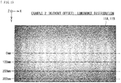
- FIG. 19 illustrates an in-plane luminance distribution in the example 2 of aspect.
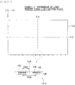
- FIG. 20 illustrates dimensions in arrangement of the second light sources 10-2 in the upper light-guiding plate 11B according to the example 2 of aspect.
- FIG. 21 illustrates dimensions in arrangement of the first light sources 10-1 in the lower light-guiding plate 11A according to the example 2 of aspect.
- FIG. 22 illustrates a luminance distribution in X direction in an example 3 of aspect.
- a vertical scale denotes luminance
- a horizontal scale denotes a distance in X direction.
- FIG. 23 illustrates an in-plane luminance distribution in the example 3 of aspect.
- FIG. 24 illustrates dimensions in arrangement of the second light sources 10-2 in the upper light-guiding plate 11B according to the example 3 of aspect.
- FIG. 25 illustrates dimensions in arrangement of the first light sources 10-1 in the lower light-guiding plate 11A according to the example 3 of aspect. It is to be noted that also in examples 4 and 5 of aspect to be hereinafter described, dimensions are similar to those illustrated in FIG. 24 and FIG. 25 .
- the optical axis positions of the first light sources 10-1 and the second light sources 10-2 in X direction are the same to each other (no offset).
- the optical axis positions of the first light sources 10-1 and the second light sources 10-2 in X direction are made different (offset) from each other.
- FIG. 26 compares coverage of dot patterns in the examples 3, 4, and 5 of aspect.
- FIG. 26 illustrates coverage of the second dot pattern 30-2 in the upper light-guiding plate 11B; however, coverage of the first dot pattern 30-1 in the lower light-guiding plate 11A may be also substantially similar to the above coverage.
- a vertical scale denotes coverage of the second dot pattern 30-2, and a horizontal scale denotes a distance in Y direction.
- FIG. 27 compares luminance distributions in Y direction in the examples 3, 4, and 5 of aspect.
- a vertical scale denotes luminance
- a horizontal scale denotes a distance in Y direction.
- FIG. 27 illustrates characteristics in a case where both the lower light-guiding plate 11A and the upper light-guiding plate 11B are illuminated and characteristics in a case where only the upper light-guiding plate 11B is illuminated.
- FIG. 28 and FIG. 29 compares normalized luminance distributions in Y direction in the examples 3, 4, and 5 of aspect.
- a vertical scale denotes normalized luminance
- a horizontal scale denotes a normalized distance in Y direction.
- FIG. 28 and FIG. 29 illustrate characteristics in a case where both the lower light-guiding plate 11A and the upper light-guiding plate 11B are illuminated and characteristics in a case where only the upper light-guiding plate 11B is illuminated.
- FIG. 30 illustrates an in-plane luminance distribution in the example 4 of aspect.
- FIG. 31 illustrates a luminance distribution in X direction in the example 4 of aspect.
- a vertical scale denotes luminance
- a horizontal scale denotes a distance in X direction.
- FIG. 32 illustrates an in-plane luminance distribution in the example 5 of aspect.
- FIG. 33 illustrates a luminance distribution in X direction in the example 5 of aspect.
- a vertical scale denotes luminance
- a horizontal scale denotes a distance in X direction.
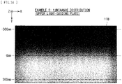
- FIG. 34 illustrates an in-plane luminance distribution of an upper light-guiding plate according to the example 3 of aspect.
- FIG. 35 illustrates a luminance distribution in X direction of the upper light-guiding plate according to the example 3 of aspect.
- a vertical scale denotes luminance
- a horizontal scale denotes a distance in X direction.
- FIG. 36 schematically illustrates a luminance distribution in the example 3 of aspect.
- FIG. 36 schematically illustrates the luminance distribution in a case where the light emission luminance of the lower light-guiding plate 11A and the light emission luminance of the upper light-guiding plate 11B are combined in the example 3 of aspect.
- FIG. 37 illustrates an in-plane luminance distribution of an upper light-guiding plate according to the example 4 of aspect.
- FIG. 38 illustrates a luminance distribution in X direction of the upper light-guiding plate according to the example 4 of aspect.
- a vertical scale denotes luminance
- a horizontal scale denotes a distance in X direction.
- FIG. 39 schematically illustrates the luminance distribution in the example 4 of aspect.
- FIG. 39 schematically illustrates the luminance distribution in a case where the light emission luminance of the lower light-guiding plate 11A and the light emission luminance of the upper light-guiding plate 11B are combined in the example 4 of aspect.
- FIG. 40 illustrates an in-plane luminance distribution of an upper light-guiding plate according to the example 5 of aspect.
- FIG. 41 illustrates a luminance distribution in X direction of the upper light-guiding plate according to the example 5 of aspect.
- a vertical scale denotes luminance
- a horizontal scale denotes a distance in X direction.
- FIG. 42 schematically illustrates a luminance distribution in the example 5 of aspect.
- FIG. 42 schematically illustrates the luminance distribution in a case where the light emission luminance of the lower light-guiding plate 11A and the light emission luminance of the upper light-guiding plate 11B are combined in the example 4 of aspect.
- each of the examples 3, 4, and 5 of aspect as a pattern, coverage of the dot patterns changes depending on distance in Y direction.
- the luminance distribution in Y direction when either the upper light-guiding plate 11B or the lower light-guiding plate 11A is only illuminated may be different in each of the examples of aspect as illustrated in FIG. 27 .
- the luminance distribution in Y direction when both the upper light-guiding plate 11B and the lower light-guiding plate 11A are illuminated is allowed to be made substantially similar in each of the examples of aspect as illustrated in FIG. 27 .
- the luminance distribution in X direction differs in each of the examples of aspect, and the luminance distribution when viewed from the plane as a whole may be different. Further, when the luminance distribution is considered as superposition of the emission luminance distributions of the lower light-guiding plate 11A and the upper light-guiding plate 11B, there may exist an optimal distribution in relation to change in luminance in Y direction. For the luminance distribution with steep change in luminance in Y direction like the example 4 of aspect illustrated in FIG. 27 , there are regions where the luminance distributions do not match in the upper- and lower light-guiding plates as illustrated in FIG. 39 .
- backlight unit 1A a light-emitting device according to a second aspect of the present disclosure.
- backlight unit 1A any component parts essentially same as those in the backlight unit 1 according to the above-described first aspect are denoted with the same reference numerals, and the related descriptions are omitted as appropriate.
- FIG. 43 illustrates an example of a cross-sectional configuration of the backlight unit 1A according to the present aspect.
- FIG. 44 illustrates an arrangement configuration in X-Y plane for the lower light-guiding plate 11A, the upper light-guiding plate 11B, the first light sources 10-1, and the second light sources 10-2 in the second aspect.
- the backlight unit 1A according to the present aspect is also provided with a wavelength conversion sheet 14.
- a configuration example of combining the red light sources 10R, green light sources 10G, and blue light sources 10B is illustrated; however, it is also possible to use only the blue light sources 10B by combined use of the wavelength conversion sheet 14.
- the wavelength conversion sheet 14 may be provided between the second light emitting surface of the upper light-guiding plate 11B and the optical sheet 13.
- the wavelength conversion sheet 14 may be made to contain, for example, a fluorescent material that converts a wavelength of a part of blue-color light as predetermined color light into any other wavelength such as red-color light, green-color light, or yellow-color light.
- white emission light may be obtained by color mixture of blue-color light as predetermined color light from the blue light sources 10B and light after wavelength conversion by the wavelength conversion sheet 14.
- FIG. 45 illustrates a specific example of arrangement of the blue light sources 10B attached to the upper light-guiding plate 11B in the present aspect.
- FIG. 46 illustrates a specific example of the arrangement of the blue light sources 10B attached to the lower light-guiding plate 11A.
- a relative position of each of the blue light sources 10B may be offset in such a manner that optical axis positions in X direction of the blue light sources 10B configuring the first light sources 10-1 and the blue light sources 10B configuring the second light sources 10-2 are different from each other.
- FIG. 47 illustrates a configuration example of light-guiding plates and light sources in the light-emitting device according to the present aspect.
- first light sources 10-1 and the second light sources 10-2 face side face in Y direction of the lower light-guiding plate 11A and the upper light-guiding plate 11B are illustrated; however, such light sources may face side face in X direction as illustrated in FIG. 47 , for example.
- a third side face S3 of the lower light-guiding plate 11A may be used as a first light incidence surface, and the first light sources 10-1 may face the third side face S3.
- a fourth side face S4 of the upper light-guiding plate 11B may be used as a second light incidence surface, and the second light sources 10-2 may face the fourth side face S4.
- the pattern density of the first light sources 10-1 and the second light sources 10-2 may be changed in X direction.
- the backlight units 1 and 1A as described above may be incorporated into a display device 2 illustrated in an example in FIG. 48 , and may be applicable to electronic apparatuses given below.
- the display device 2 may be, for example, a liquid crystal display.
- a configuration may be made in such a manner that polarization plates 21a and 21b are stacked on a light entry side and a light exit side of a liquid crystal panel 20, and the backlight units 1 and 1A illuminate the liquid crystal panel 20 from behind.
- Examples of electronic apparatuses may include electronic apparatuses, such as a television, an electronic book, a smartphone, a digital camera, a notebook personal computer, a video camera, and a mobile phone that are described below.
- the display device 2 using the above-described backlight units 1 and 1A is applicable to electronic apparatuses in every field that display externally inputted image signals or internally generated image signals as images or video pictures.
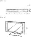
- FIG. 49 illustrates an electronic apparatus to be used as a television, and this television has a configuration in which a flat tabular main body section 102 for image display is supported by a stand 103.
- the illustrated television is used as a stationary type to be placed on a level surface such as a floor, a shelf, or a table with the stand 103 attached to the main body section 102; however, such a television may be also used as a wall-mounted type with the stand 103 detached from the main body section 102.
- the main body section 102 is configured to include the above-described display device 2.
- FIG. 50 illustrates an external appearance of an electronic book.
- FIG. 51 illustrates an external appearance of another electronic book.
- Any of these electronic books may have, for example, a display section 210 and a non-display section 220, and the display section 210 is constituted by the above-described display device 2.
- FIG. 52 illustrates an external appearance of a smartphone.
- This smartphone may have, for example, a display section 230 and a non-display section 240, and the display section 230 is constituted by the above-described display device 2.
- FIG. 53 and FIG. 54 illustrates an external appearance of a digital camera.
- FIG. 53 illustrates an external appearance viewed from the front side (subject side) of the digital camera
- FIG. 54 illustrates an external appearance viewed from the backside (image side) of the digital camera.
- This digital camera may have, for example, a light-emitting section 410 for flashing, a display section 420, a menu switch 430, and a shutter button 440, and the display section 420 is constituted by the above-described display device 2.
- FIG. 55 illustrates an external appearance of a notebook personal computer.
- This notebook personal computer may have, for example, a main unit 510, a keyboard 520 for operation of entering characters etc., and a display section 530 for displaying images, and the display section 530 is constituted by the above-described display device 2.
- FIG. 56 illustrates an external appearance of a video camera.
- This video camera may have, for example, a main unit section 610, a lens 620 provided at a front lateral surface of this main unit section 610 and for shooting an image of a subject, a shooting start and stop switch 630, and a display section 640.
- the display section 640 is constituted by the above-described display device 2.
- FIG. 57 and FIG. 58 illustrates an external appearance of a mobile phone.
- this mobile phone may join an upper chassis 710 and a lower chassis 720 by means of a connecting section (hinge section) 730, and may have a display 740, a sub-display 750, a picture light 760, and a camera 770.
- the display 740 or the sub-display 750 of these component parts is constituted by the above-described display device 2.
Claims (11)
- Dispositif électroluminescent (1), comprenant :une première plaque de guidage de lumière (11A) ayant une première surface d'incidence de lumière (S1), une première surface électroluminescente (S12) qui émet de la lumière vers une direction d'émission de lumière prédéterminée, et une première surface d'amélioration d'émission de lumière (S13) pourvue d'un premier motif ;une seconde plaque de guidage de lumière (11B) ayant une seconde surface d'incidence de lumière (S2), une seconde surface électroluminescente (S22) qui émet de la lumière vers la direction d'émission de lumière, et une seconde surface d'amélioration d'émission de lumière (S23) pourvue d'un second motif, la seconde plaque de guidage de lumière (11A) faisant face à la première plaque de guidage de lumière (11B) ;une pluralité de premières sources de lumière (10-1) faisant face à la première surface d'incidence de lumière (S1) ; etune pluralité de secondes sources de lumière (10-2) faisant face à la seconde surface d'incidence de lumière (S2),le premier motif étant un motif comprenant une pluralité de premières sections punctiformes dont un pas d'agencement change pour faire en sorte que la densité des premières sections punctiformes augmente à mesure qu'une distance depuis la première surface d'incidence de lumière (S1) augmente,le second motif étant un motif comprenant une pluralité de secondes sections punctiformes dont le pas d'agencement change pour que la densité des secondes sections punctiformes augmente lorsque la distance à la seconde surface d'incidence de lumière (S2) augmente, etlorsqu'elles sont observées dans la direction d'émission de la lumière, les régions pourvues du premier motif et du second motif se chevauchant partiellement, et les directions dans lesquelles les densités du premier motif et du second motif augmentent étant opposées l'une à l'autre,la pluralité de premières sections punctiformes changeant d'agencement de pas de sorte que leur densité augmente à mesure qu'une distance de la première surface d'incidence de lumière (S1) augmente,la pluralité de secondes sections punctiformes changeant d'agencement de pas de sorte que leur densité augmente à mesure qu'une distance de la seconde surface d'incidence de lumière augmente (S2), caractérisé en ce quela pluralité de premières sections punctiformes change de taille de sorte que leur densité augmente à mesure qu'une distance de la première surface d'incidence de lumière (S1) augmente, en ce que la pluralité de secondes sections punctiformes change de taille de sorte que leur densité augmente à mesure qu'une distance de la seconde surface d'incidence de lumière augmente (S2), et en ce quedes positions des axes optiques des premières sources de lumière (10-1) et des positions des axes optiques des secondes sources de lumière (10-2) sont décalées les unes par rapport aux autres lorsqu'elles sont observées dans la direction d'émission de la lumière.
- Dispositif électroluminescent (1) selon la revendication 1,chaque nombre prédéterminé des premières sources de lumière (10-1) et des secondes sources de lumière (10-2) configurant respectivement une unité de source de lumière (10U), etdes positions des axes optiques des premières sources de lumière (10-1) dans l'une des unités de source de lumière (10U) et des positions des axes optiques des secondes sources de lumière (10-2) dans une unité de source de lumière correspondante (10U) étant différentes les unes des autres.
- Dispositif électroluminescent (1) selon la revendication 1, chacune des plaques de guidage de lumière (11A, 11B) ayant en outre une face latérale faisant face à chacune des surfaces d'incidence de lumière (S1, S2), et la luminance à une position arbitraire dans un plan d'observation orthogonal à la direction d'émission de lumière satisfaisant aux conditions données ci-dessous :lorsque y < 0,
 lorsque y ≥ 0,
 L max=1, et L min=0y étant une position dans une direction de guidage de lumière, dans chacune des plaques de guidage de lumière (11A, 11B) lorsqu'elles sont observées dans la direction d'émission de la lumière, dans la direction de guidage de lumière de chacune des plaques de guidage de lumière (11A, 11B), une position de chacune des surfaces d'incidence de lumière (S1, S2) étant -1, un centre étant 0, et une position d'une face latérale faisant face à chacune des surfaces d'incidence de lumière (S1, S2) étant 1,L étant un rapport de luminance, un rapport de luminance à la position arbitraire lorsque soit les premières sources de lumière (10-1) soit les secondes sources de lumière (10-2) sont seulement allumées, lorsque la luminance à la position arbitraire dans le plan d'observation lorsque les premières et secondes sources de lumière (10-1, 10-2) sont allumées est 1,L max étant une valeur maximale de L, etL min étant une valeur minimale de L.
 - Dispositif électroluminescent (1) selon la revendication 1, les premières sources de lumière (10-1) et les secondes sources de lumière (10-2) émettant de la lumière vers des directions opposées l'une à l'autre lorsqu'elles sont observées dans la direction d'émission de la lumière.
- Dispositif électroluminescent (1) selon la revendication 1, chacune de la pluralité de premières sources de lumière (10-1) et de la pluralité de secondes sources de lumière (10-2) comprenant une diode laser qui émet une lumière de couleur rouge, une diode laser qui émet une lumière de couleur verte, et une diode laser qui émet une lumière de couleur bleue.
- Dispositif électroluminescent (1) selon la revendication 1, comprenant en outre une feuille de conversion de longueur d'onde (14) faisant face à la seconde plaque de guidage de lumière (11B),chacune de la pluralité de premières sources de lumière (10-1) et de la pluralité de secondes sources de lumière (10-2) étant une diode laser émettant une lumière de couleur prédéterminée, etla feuille de conversion de longueur d'onde (14) convertissant la lumière de couleur prédéterminée en une autre lumière de couleur.
- Dispositif d'affichage (2) comprenant un panneau d'affichage et le dispositif électroluminescent (1) selon l'une quelconque des revendications 1 à 6, le dispositif électroluminescent (1) éclairant le panneau d'affichage.
- Dispositif d'affichage (2) selon la revendication 7, le dispositif électroluminescent (1) comprenant en outre une feuille optique (13) configurée pour faire face à la seconde surface d'incidence de lumière (S2) de la seconde plaque de guidage de lumière (11B), et une feuille de conversion de longueur d'onde (14) prévue entre la seconde surface électroluminescente (S22) de la seconde plaque de guidage de lumière (11B) et la feuille optique (13), la feuille de conversion de longueur d'onde (14) contenant un matériau fluorescent qui convertit une longueur d'onde d'une partie de la lumière de couleur bleue comme lumière de couleur prédéterminée en une autre longueur d'onde.
- Dispositif d'affichage (2) selon la revendication 8, l'autre longueur d'onde comprenant une lumière de couleur rouge, une lumière de couleur verte ou une lumière de couleur jaune.
- Dispositif d'affichage (2) selon la revendication 7, le dispositif électroluminescent (1) comprenant en outre une feuille réfléchissante (12) qui est un élément tabulaire ou plan configuré pour faire face à la première surface d'amélioration d'émission de lumière (S13) de la première plaque de guidage de lumière (11A), et une feuille optique (13) configurée pour faire face à la seconde surface d'incidence de lumière (S2) de la seconde plaque de guidage de lumière (11B).
- Dispositif d'affichage (2) selon la revendication 10, la feuille optique (13) comprenant une plaque de diffusion, une feuille de diffusion, un film de lentille, et une feuille de séparation de polarisation.
Applications Claiming Priority (2)
| Application Number | Priority Date | Filing Date | Title |
|---|---|---|---|
| JP2014057460 | 2014-03-20 | ||
| PCT/JP2015/052944 WO2015141304A1 (fr) | 2014-03-20 | 2015-02-03 | Dispositif électroluminescent et dispositif d'affichage |
Publications (3)
| Publication Number | Publication Date |
|---|---|
| EP3133333A1 EP3133333A1 (fr) | 2017-02-22 |
| EP3133333A4 EP3133333A4 (fr) | 2018-04-04 |
| EP3133333B1 true EP3133333B1 (fr) | 2022-04-06 |
Family
ID=54144284
Family Applications (1)
| Application Number | Title | Priority Date | Filing Date |
|---|---|---|---|
| EP15764759.5A Active EP3133333B1 (fr) | 2014-03-20 | 2015-02-03 | Dispositif électroluminescent et dispositif d'affichage |
Country Status (4)
| Country | Link |
|---|---|
| US (1) | US10031275B2 (fr) |
| EP (1) | EP3133333B1 (fr) |
| JP (1) | JP6586950B2 (fr) |
| WO (1) | WO2015141304A1 (fr) |
Families Citing this family (1)
| Publication number | Priority date | Publication date | Assignee | Title |
|---|---|---|---|---|
| CN108132564B (zh) * | 2018-01-23 | 2020-12-18 | 京东方科技集团股份有限公司 | 一种导光结构、背光源及显示装置 |
Citations (2)
| Publication number | Priority date | Publication date | Assignee | Title |
|---|---|---|---|---|
| JP2004342454A (ja) * | 2003-05-15 | 2004-12-02 | Sharp Corp | 発光装置及びこの発光装置を用いた表示装置 |
| US20070064417A1 (en) * | 2003-12-15 | 2007-03-22 | Masato Hatanaka | Lighting system and back-light device using this lighting system |
Family Cites Families (14)
| Publication number | Priority date | Publication date | Assignee | Title |
|---|---|---|---|---|
| JPH036525A (ja) * | 1989-06-02 | 1991-01-14 | Mitsubishi Petrochem Co Ltd | バックライト装置 |
| GB9807204D0 (en) * | 1998-04-04 | 1998-06-03 | Ici Plc | An edge-lit illumination system |
| US6816145B1 (en) * | 1998-07-22 | 2004-11-09 | Silicon Graphics, Inc. | Large area wide aspect ratio flat panel monitor having high resolution for high information content display |
| JP2000268617A (ja) * | 1999-03-12 | 2000-09-29 | Ichikoh Ind Ltd | 平面カラー発光装置 |
| TWI321694B (en) * | 2005-12-23 | 2010-03-11 | Innolux Display Corp | Backlight module and liquid crystal display module |
| KR20080090961A (ko) * | 2006-01-27 | 2008-10-09 | 가부시키가이샤 엔프라스 | 면광원 장치 및 표시 장치 |
| JP4513918B2 (ja) * | 2008-06-03 | 2010-07-28 | エプソンイメージングデバイス株式会社 | 照明装置及び電気光学装置 |
| JP2011018619A (ja) * | 2009-07-10 | 2011-01-27 | Sony Corp | 表示装置及び面照明装置 |
| JP2011181794A (ja) * | 2010-03-03 | 2011-09-15 | Panasonic Corp | 発光装置及びそれを用いたバックライトモジュール |
| JP2011238484A (ja) | 2010-05-11 | 2011-11-24 | Mitsubishi Electric Corp | バックライト装置および液晶表示装置 |
| KR101384052B1 (ko) * | 2010-09-14 | 2014-04-09 | 파나소닉 주식회사 | 백라이트 장치, 및 그 백라이트 장치를 이용한 액정 표시 장치, 및 그들에 이용하는 발광 다이오드 |
| US20120140436A1 (en) * | 2010-12-02 | 2012-06-07 | Intematix Corporation | Solid-state lamps with light guide and photoluminescence material |
| KR101850431B1 (ko) * | 2011-07-07 | 2018-05-31 | 엘지이노텍 주식회사 | 발광 모듈 및 이를 포함하는 조명 시스템 |
| JP5738742B2 (ja) * | 2011-11-09 | 2015-06-24 | 株式会社東芝 | 面光源装置 |
-
2015
- 2015-02-03 WO PCT/JP2015/052944 patent/WO2015141304A1/fr active Application Filing
- 2015-02-03 EP EP15764759.5A patent/EP3133333B1/fr active Active
- 2015-02-03 JP JP2016508579A patent/JP6586950B2/ja active Active
- 2015-02-03 US US15/125,680 patent/US10031275B2/en active Active
Patent Citations (2)
| Publication number | Priority date | Publication date | Assignee | Title |
|---|---|---|---|---|
| JP2004342454A (ja) * | 2003-05-15 | 2004-12-02 | Sharp Corp | 発光装置及びこの発光装置を用いた表示装置 |
| US20070064417A1 (en) * | 2003-12-15 | 2007-03-22 | Masato Hatanaka | Lighting system and back-light device using this lighting system |
Also Published As
| Publication number | Publication date |
|---|---|
| JP6586950B2 (ja) | 2019-10-09 |
| WO2015141304A1 (fr) | 2015-09-24 |
| EP3133333A1 (fr) | 2017-02-22 |
| JPWO2015141304A1 (ja) | 2017-04-06 |
| US10031275B2 (en) | 2018-07-24 |
| EP3133333A4 (fr) | 2018-04-04 |
| US20170010402A1 (en) | 2017-01-12 |
Similar Documents
| Publication | Publication Date | Title |
|---|---|---|
| JP6956229B2 (ja) | 発光装置、表示装置および照明装置 | |
| JP2022180372A (ja) | 照明装置および表示装置 | |
| US9618687B2 (en) | Light-emitting unit and display | |
| JP6265055B2 (ja) | 発光装置、表示装置および照明装置 | |
| EP2650720A1 (fr) | Dispositif émetteur de lumière, unité d'affichage et unité d'éclairage | |
| CN107980184B (zh) | 发光装置、显示装置和照明装置 | |
| JP2013218954A (ja) | 発光装置、表示装置および照明装置 | |
| JP2013218952A (ja) | 発光装置、表示装置および照明装置 | |
| US9927567B2 (en) | Display with additional lighting effects | |
| CN113168040A (zh) | 用于光导的输出耦合结构 | |
| CN117234004A (zh) | 发光装置、显示装置以及照明装置 | |
| CN113168815B (zh) | Led背光系统 | |
| JP2014225379A (ja) | 発光装置、表示装置および照明装置 | |
| EP3133333B1 (fr) | Dispositif électroluminescent et dispositif d'affichage | |
| US10788612B2 (en) | Light-emitting unit, display apparatus, and lighting apparatus | |
| JP6961754B2 (ja) | 表示装置および発光装置 | |
| JP2015146294A (ja) | 照明装置および表示装置 | |
| JP2006059583A (ja) | バックライト装置 | |
| WO2016111086A1 (fr) | Dispositif électroluminescent, dispositif d'affichage et dispositif d'éclairage |
Legal Events
| Date | Code | Title | Description |
|---|---|---|---|
| STAA | Information on the status of an ep patent application or granted ep patent |
Free format text: STATUS: THE INTERNATIONAL PUBLICATION HAS BEEN MADE |
|
| PUAI | Public reference made under article 153(3) epc to a published international application that has entered the european phase |
Free format text: ORIGINAL CODE: 0009012 |
|
| STAA | Information on the status of an ep patent application or granted ep patent |
Free format text: STATUS: REQUEST FOR EXAMINATION WAS MADE |
|
| 17P | Request for examination filed |
Effective date: 20160907 |
|
| AK | Designated contracting states |
Kind code of ref document: A1 Designated state(s): AL AT BE BG CH CY CZ DE DK EE ES FI FR GB GR HR HU IE IS IT LI LT LU LV MC MK MT NL NO PL PT RO RS SE SI SK SM TR |
|
| AX | Request for extension of the european patent |
Extension state: BA ME |
|
| DAX | Request for extension of the european patent (deleted) | ||
| A4 | Supplementary search report drawn up and despatched |
Effective date: 20180305 |
|
| RIC1 | Information provided on ipc code assigned before grant |
Ipc: F21Y 103/00 20160101ALI20180227BHEP Ipc: F21Y 101/00 20160101ALI20180227BHEP Ipc: F21V 8/00 20060101ALI20180227BHEP Ipc: G02F 1/13357 20060101ALI20180227BHEP Ipc: F21S 2/00 20160101AFI20180227BHEP |
|
| STAA | Information on the status of an ep patent application or granted ep patent |
Free format text: STATUS: EXAMINATION IS IN PROGRESS |
|
| 17Q | First examination report despatched |
Effective date: 20190426 |
|
| STAA | Information on the status of an ep patent application or granted ep patent |
Free format text: STATUS: EXAMINATION IS IN PROGRESS |
|
| RAP3 | Party data changed (applicant data changed or rights of an application transferred) |
Owner name: SONY GROUP CORPORATION |
|
| GRAP | Despatch of communication of intention to grant a patent |
Free format text: ORIGINAL CODE: EPIDOSNIGR1 |
|
| STAA | Information on the status of an ep patent application or granted ep patent |
Free format text: STATUS: GRANT OF PATENT IS INTENDED |
|
| INTG | Intention to grant announced |
Effective date: 20210901 |
|
| GRAJ | Information related to disapproval of communication of intention to grant by the applicant or resumption of examination proceedings by the epo deleted |
Free format text: ORIGINAL CODE: EPIDOSDIGR1 |
|
| STAA | Information on the status of an ep patent application or granted ep patent |
Free format text: STATUS: EXAMINATION IS IN PROGRESS |
|
| GRAP | Despatch of communication of intention to grant a patent |
Free format text: ORIGINAL CODE: EPIDOSNIGR1 |
|
| STAA | Information on the status of an ep patent application or granted ep patent |
Free format text: STATUS: GRANT OF PATENT IS INTENDED |
|
| GRAJ | Information related to disapproval of communication of intention to grant by the applicant or resumption of examination proceedings by the epo deleted |
Free format text: ORIGINAL CODE: EPIDOSDIGR1 |
|
| STAA | Information on the status of an ep patent application or granted ep patent |
Free format text: STATUS: EXAMINATION IS IN PROGRESS |
|
| INTC | Intention to grant announced (deleted) | ||
| INTG | Intention to grant announced |
Effective date: 20211207 |
|
| INTC | Intention to grant announced (deleted) | ||
| GRAP | Despatch of communication of intention to grant a patent |
Free format text: ORIGINAL CODE: EPIDOSNIGR1 |
|
| STAA | Information on the status of an ep patent application or granted ep patent |
Free format text: STATUS: GRANT OF PATENT IS INTENDED |
|
| GRAS | Grant fee paid |
Free format text: ORIGINAL CODE: EPIDOSNIGR3 |
|
| GRAA | (expected) grant |
Free format text: ORIGINAL CODE: 0009210 |
|
| STAA | Information on the status of an ep patent application or granted ep patent |
Free format text: STATUS: THE PATENT HAS BEEN GRANTED |
|
| INTG | Intention to grant announced |
Effective date: 20220209 |
|
| AK | Designated contracting states |
Kind code of ref document: B1 Designated state(s): AL AT BE BG CH CY CZ DE DK EE ES FI FR GB GR HR HU IE IS IT LI LT LU LV MC MK MT NL NO PL PT RO RS SE SI SK SM TR |
|
| REG | Reference to a national code |
Ref country code: GB Ref legal event code: FG4D |
|
| REG | Reference to a national code |
Ref country code: CH Ref legal event code: EP |
|
| REG | Reference to a national code |
Ref country code: AT Ref legal event code: REF Ref document number: 1481660 Country of ref document: AT Kind code of ref document: T Effective date: 20220415 |
|
| REG | Reference to a national code |
Ref country code: DE Ref legal event code: R096 Ref document number: 602015078050 Country of ref document: DE |
|
| REG | Reference to a national code |
Ref country code: IE Ref legal event code: FG4D |
|
| REG | Reference to a national code |
Ref country code: NL Ref legal event code: FP |
|
| REG | Reference to a national code |
Ref country code: LT Ref legal event code: MG9D |
|
| REG | Reference to a national code |
Ref country code: AT Ref legal event code: MK05 Ref document number: 1481660 Country of ref document: AT Kind code of ref document: T Effective date: 20220406 |
|
| PG25 | Lapsed in a contracting state [announced via postgrant information from national office to epo] |
Ref country code: SE Free format text: LAPSE BECAUSE OF FAILURE TO SUBMIT A TRANSLATION OF THE DESCRIPTION OR TO PAY THE FEE WITHIN THE PRESCRIBED TIME-LIMIT Effective date: 20220406 Ref country code: PT Free format text: LAPSE BECAUSE OF FAILURE TO SUBMIT A TRANSLATION OF THE DESCRIPTION OR TO PAY THE FEE WITHIN THE PRESCRIBED TIME-LIMIT Effective date: 20220808 Ref country code: NO Free format text: LAPSE BECAUSE OF FAILURE TO SUBMIT A TRANSLATION OF THE DESCRIPTION OR TO PAY THE FEE WITHIN THE PRESCRIBED TIME-LIMIT Effective date: 20220706 Ref country code: LT Free format text: LAPSE BECAUSE OF FAILURE TO SUBMIT A TRANSLATION OF THE DESCRIPTION OR TO PAY THE FEE WITHIN THE PRESCRIBED TIME-LIMIT Effective date: 20220406 Ref country code: HR Free format text: LAPSE BECAUSE OF FAILURE TO SUBMIT A TRANSLATION OF THE DESCRIPTION OR TO PAY THE FEE WITHIN THE PRESCRIBED TIME-LIMIT Effective date: 20220406 Ref country code: GR Free format text: LAPSE BECAUSE OF FAILURE TO SUBMIT A TRANSLATION OF THE DESCRIPTION OR TO PAY THE FEE WITHIN THE PRESCRIBED TIME-LIMIT Effective date: 20220707 Ref country code: FI Free format text: LAPSE BECAUSE OF FAILURE TO SUBMIT A TRANSLATION OF THE DESCRIPTION OR TO PAY THE FEE WITHIN THE PRESCRIBED TIME-LIMIT Effective date: 20220406 Ref country code: ES Free format text: LAPSE BECAUSE OF FAILURE TO SUBMIT A TRANSLATION OF THE DESCRIPTION OR TO PAY THE FEE WITHIN THE PRESCRIBED TIME-LIMIT Effective date: 20220406 Ref country code: BG Free format text: LAPSE BECAUSE OF FAILURE TO SUBMIT A TRANSLATION OF THE DESCRIPTION OR TO PAY THE FEE WITHIN THE PRESCRIBED TIME-LIMIT Effective date: 20220706 Ref country code: AT Free format text: LAPSE BECAUSE OF FAILURE TO SUBMIT A TRANSLATION OF THE DESCRIPTION OR TO PAY THE FEE WITHIN THE PRESCRIBED TIME-LIMIT Effective date: 20220406 |
|
| PG25 | Lapsed in a contracting state [announced via postgrant information from national office to epo] |
Ref country code: RS Free format text: LAPSE BECAUSE OF FAILURE TO SUBMIT A TRANSLATION OF THE DESCRIPTION OR TO PAY THE FEE WITHIN THE PRESCRIBED TIME-LIMIT Effective date: 20220406 Ref country code: PL Free format text: LAPSE BECAUSE OF FAILURE TO SUBMIT A TRANSLATION OF THE DESCRIPTION OR TO PAY THE FEE WITHIN THE PRESCRIBED TIME-LIMIT Effective date: 20220406 Ref country code: LV Free format text: LAPSE BECAUSE OF FAILURE TO SUBMIT A TRANSLATION OF THE DESCRIPTION OR TO PAY THE FEE WITHIN THE PRESCRIBED TIME-LIMIT Effective date: 20220406 Ref country code: IS Free format text: LAPSE BECAUSE OF FAILURE TO SUBMIT A TRANSLATION OF THE DESCRIPTION OR TO PAY THE FEE WITHIN THE PRESCRIBED TIME-LIMIT Effective date: 20220806 |
|
| REG | Reference to a national code |
Ref country code: DE Ref legal event code: R097 Ref document number: 602015078050 Country of ref document: DE |
|
| PG25 | Lapsed in a contracting state [announced via postgrant information from national office to epo] |
Ref country code: SM Free format text: LAPSE BECAUSE OF FAILURE TO SUBMIT A TRANSLATION OF THE DESCRIPTION OR TO PAY THE FEE WITHIN THE PRESCRIBED TIME-LIMIT Effective date: 20220406 Ref country code: SK Free format text: LAPSE BECAUSE OF FAILURE TO SUBMIT A TRANSLATION OF THE DESCRIPTION OR TO PAY THE FEE WITHIN THE PRESCRIBED TIME-LIMIT Effective date: 20220406 Ref country code: RO Free format text: LAPSE BECAUSE OF FAILURE TO SUBMIT A TRANSLATION OF THE DESCRIPTION OR TO PAY THE FEE WITHIN THE PRESCRIBED TIME-LIMIT Effective date: 20220406 Ref country code: EE Free format text: LAPSE BECAUSE OF FAILURE TO SUBMIT A TRANSLATION OF THE DESCRIPTION OR TO PAY THE FEE WITHIN THE PRESCRIBED TIME-LIMIT Effective date: 20220406 Ref country code: DK Free format text: LAPSE BECAUSE OF FAILURE TO SUBMIT A TRANSLATION OF THE DESCRIPTION OR TO PAY THE FEE WITHIN THE PRESCRIBED TIME-LIMIT Effective date: 20220406 Ref country code: CZ Free format text: LAPSE BECAUSE OF FAILURE TO SUBMIT A TRANSLATION OF THE DESCRIPTION OR TO PAY THE FEE WITHIN THE PRESCRIBED TIME-LIMIT Effective date: 20220406 |
|
| PLBE | No opposition filed within time limit |
Free format text: ORIGINAL CODE: 0009261 |
|
| STAA | Information on the status of an ep patent application or granted ep patent |
Free format text: STATUS: NO OPPOSITION FILED WITHIN TIME LIMIT |
|
| 26N | No opposition filed |
Effective date: 20230110 |
|
| PG25 | Lapsed in a contracting state [announced via postgrant information from national office to epo] |
Ref country code: AL Free format text: LAPSE BECAUSE OF FAILURE TO SUBMIT A TRANSLATION OF THE DESCRIPTION OR TO PAY THE FEE WITHIN THE PRESCRIBED TIME-LIMIT Effective date: 20220406 |
|
| PGFP | Annual fee paid to national office [announced via postgrant information from national office to epo] |
Ref country code: NL Payment date: 20230222 Year of fee payment: 9 |
|
| PGFP | Annual fee paid to national office [announced via postgrant information from national office to epo] |
Ref country code: FR Payment date: 20230223 Year of fee payment: 9 |
|
| PG25 | Lapsed in a contracting state [announced via postgrant information from national office to epo] |
Ref country code: SI Free format text: LAPSE BECAUSE OF FAILURE TO SUBMIT A TRANSLATION OF THE DESCRIPTION OR TO PAY THE FEE WITHIN THE PRESCRIBED TIME-LIMIT Effective date: 20220406 |
|
| PGFP | Annual fee paid to national office [announced via postgrant information from national office to epo] |
Ref country code: GB Payment date: 20230214 Year of fee payment: 9 Ref country code: DE Payment date: 20230227 Year of fee payment: 9 |
|
| P01 | Opt-out of the competence of the unified patent court (upc) registered |
Effective date: 20230514 |
|
| PG25 | Lapsed in a contracting state [announced via postgrant information from national office to epo] |
Ref country code: MC Free format text: LAPSE BECAUSE OF FAILURE TO SUBMIT A TRANSLATION OF THE DESCRIPTION OR TO PAY THE FEE WITHIN THE PRESCRIBED TIME-LIMIT Effective date: 20220406 |
|
| REG | Reference to a national code |
Ref country code: CH Ref legal event code: PL |
|
| REG | Reference to a national code |
Ref country code: BE Ref legal event code: MM Effective date: 20230228 |
|
| PG25 | Lapsed in a contracting state [announced via postgrant information from national office to epo] |
Ref country code: LU Free format text: LAPSE BECAUSE OF NON-PAYMENT OF DUE FEES Effective date: 20230203 Ref country code: LI Free format text: LAPSE BECAUSE OF NON-PAYMENT OF DUE FEES Effective date: 20230228 Ref country code: CH Free format text: LAPSE BECAUSE OF NON-PAYMENT OF DUE FEES Effective date: 20230228 |
|
| REG | Reference to a national code |
Ref country code: IE Ref legal event code: MM4A |
|
| PG25 | Lapsed in a contracting state [announced via postgrant information from national office to epo] |
Ref country code: IT Free format text: LAPSE BECAUSE OF FAILURE TO SUBMIT A TRANSLATION OF THE DESCRIPTION OR TO PAY THE FEE WITHIN THE PRESCRIBED TIME-LIMIT Effective date: 20220406 Ref country code: IE Free format text: LAPSE BECAUSE OF NON-PAYMENT OF DUE FEES Effective date: 20230203 |
|
| PG25 | Lapsed in a contracting state [announced via postgrant information from national office to epo] |
Ref country code: BE Free format text: LAPSE BECAUSE OF NON-PAYMENT OF DUE FEES Effective date: 20230228 |