EP3132461B1 - High voltage switching device with auxiliary nozzle - Google Patents
High voltage switching device with auxiliary nozzle Download PDFInfo
- Publication number
- EP3132461B1 EP3132461B1 EP15741875.7A EP15741875A EP3132461B1 EP 3132461 B1 EP3132461 B1 EP 3132461B1 EP 15741875 A EP15741875 A EP 15741875A EP 3132461 B1 EP3132461 B1 EP 3132461B1
- Authority
- EP
- European Patent Office
- Prior art keywords
- shield
- switching device
- contact
- auxiliary nozzle
- insulating body
- Prior art date
- Legal status (The legal status is an assumption and is not a legal conclusion. Google has not performed a legal analysis and makes no representation as to the accuracy of the status listed.)
- Active
Links
- 241000722921 Tulipa gesneriana Species 0.000 claims description 90
- 239000000463 material Substances 0.000 claims description 25
- 238000010438 heat treatment Methods 0.000 claims description 22
- 238000002679 ablation Methods 0.000 claims description 10
- 239000004020 conductor Substances 0.000 claims description 5
- 239000004922 lacquer Substances 0.000 claims description 3
- 239000011248 coating agent Substances 0.000 claims description 2
- 238000000576 coating method Methods 0.000 claims description 2
- 239000007769 metal material Substances 0.000 claims description 2
- 229910052751 metal Inorganic materials 0.000 description 18
- 239000002184 metal Substances 0.000 description 18
- 229920001343 polytetrafluoroethylene Polymers 0.000 description 16
- 239000004810 polytetrafluoroethylene Substances 0.000 description 15
- 239000007789 gas Substances 0.000 description 14
- 230000005684 electric field Effects 0.000 description 12
- 238000000034 method Methods 0.000 description 11
- 230000008569 process Effects 0.000 description 8
- 238000011084 recovery Methods 0.000 description 8
- 230000003628 erosive effect Effects 0.000 description 7
- 229920000642 polymer Polymers 0.000 description 7
- 229920001774 Perfluoroether Polymers 0.000 description 6
- 239000000919 ceramic Substances 0.000 description 6
- IYRWEQXVUNLMAY-UHFFFAOYSA-N fluoroketone group Chemical group FC(=O)F IYRWEQXVUNLMAY-UHFFFAOYSA-N 0.000 description 6
- 239000004065 semiconductor Substances 0.000 description 6
- MDQRDWAGHRLBPA-UHFFFAOYSA-N fluoroamine Chemical compound FN MDQRDWAGHRLBPA-UHFFFAOYSA-N 0.000 description 5
- -1 polytetrafluoroethylene Polymers 0.000 description 5
- RYGMFSIKBFXOCR-UHFFFAOYSA-N Copper Chemical compound [Cu] RYGMFSIKBFXOCR-UHFFFAOYSA-N 0.000 description 4
- 230000000181 anti-adherent effect Effects 0.000 description 4
- 230000008901 benefit Effects 0.000 description 4
- 238000001816 cooling Methods 0.000 description 4
- 229910052802 copper Inorganic materials 0.000 description 4
- 239000010949 copper Substances 0.000 description 4
- 230000007423 decrease Effects 0.000 description 4
- 230000013011 mating Effects 0.000 description 4
- 239000000203 mixture Substances 0.000 description 4
- JECYNCQXXKQDJN-UHFFFAOYSA-N 2-(2-methylhexan-2-yloxymethyl)oxirane Chemical compound CCCCC(C)(C)OCC1CO1 JECYNCQXXKQDJN-UHFFFAOYSA-N 0.000 description 3
- 238000007664 blowing Methods 0.000 description 3
- 239000000872 buffer Substances 0.000 description 3
- 239000012212 insulator Substances 0.000 description 3
- 238000004519 manufacturing process Methods 0.000 description 3
- 239000000243 solution Substances 0.000 description 3
- WFKWXMTUELFFGS-UHFFFAOYSA-N tungsten Chemical compound [W] WFKWXMTUELFFGS-UHFFFAOYSA-N 0.000 description 3
- IAYPIBMASNFSPL-UHFFFAOYSA-N Ethylene oxide Chemical compound C1CO1 IAYPIBMASNFSPL-UHFFFAOYSA-N 0.000 description 2
- KRHYYFGTRYWZRS-UHFFFAOYSA-N Fluorane Chemical compound F KRHYYFGTRYWZRS-UHFFFAOYSA-N 0.000 description 2
- XEEYBQQBJWHFJM-UHFFFAOYSA-N Iron Chemical compound [Fe] XEEYBQQBJWHFJM-UHFFFAOYSA-N 0.000 description 2
- 239000000956 alloy Substances 0.000 description 2
- 229910045601 alloy Inorganic materials 0.000 description 2
- 230000015572 biosynthetic process Effects 0.000 description 2
- 239000002800 charge carrier Substances 0.000 description 2
- 239000003638 chemical reducing agent Substances 0.000 description 2
- 238000009826 distribution Methods 0.000 description 2
- 238000010891 electric arc Methods 0.000 description 2
- 238000009713 electroplating Methods 0.000 description 2
- 238000005516 engineering process Methods 0.000 description 2
- 239000012530 fluid Substances 0.000 description 2
- 238000009413 insulation Methods 0.000 description 2
- 229910052721 tungsten Inorganic materials 0.000 description 2
- 239000010937 tungsten Substances 0.000 description 2
- LOUICXNAWQPGSU-UHFFFAOYSA-N 2,2,3,3-tetrafluorooxirane Chemical class FC1(F)OC1(F)F LOUICXNAWQPGSU-UHFFFAOYSA-N 0.000 description 1
- VYZAMTAEIAYCRO-UHFFFAOYSA-N Chromium Chemical compound [Cr] VYZAMTAEIAYCRO-UHFFFAOYSA-N 0.000 description 1
- BQCADISMDOOEFD-UHFFFAOYSA-N Silver Chemical compound [Ag] BQCADISMDOOEFD-UHFFFAOYSA-N 0.000 description 1
- KEAYESYHFKHZAL-UHFFFAOYSA-N Sodium Chemical compound [Na] KEAYESYHFKHZAL-UHFFFAOYSA-N 0.000 description 1
- 229910000831 Steel Inorganic materials 0.000 description 1
- 239000002253 acid Substances 0.000 description 1
- 230000009471 action Effects 0.000 description 1
- 239000000853 adhesive Substances 0.000 description 1
- 230000001070 adhesive effect Effects 0.000 description 1
- 229910052783 alkali metal Inorganic materials 0.000 description 1
- 150000001340 alkali metals Chemical class 0.000 description 1
- 229910052782 aluminium Inorganic materials 0.000 description 1
- XAGFODPZIPBFFR-UHFFFAOYSA-N aluminium Chemical compound [Al] XAGFODPZIPBFFR-UHFFFAOYSA-N 0.000 description 1
- 230000005540 biological transmission Effects 0.000 description 1
- 239000003990 capacitor Substances 0.000 description 1
- 239000006229 carbon black Substances 0.000 description 1
- 239000012159 carrier gas Substances 0.000 description 1
- 229910010293 ceramic material Inorganic materials 0.000 description 1
- 230000008859 change Effects 0.000 description 1
- 229910052804 chromium Inorganic materials 0.000 description 1
- 239000011651 chromium Substances 0.000 description 1
- 150000001875 compounds Chemical class 0.000 description 1
- 239000002322 conducting polymer Substances 0.000 description 1
- 229920001940 conductive polymer Polymers 0.000 description 1
- 239000000112 cooling gas Substances 0.000 description 1
- 238000000354 decomposition reaction Methods 0.000 description 1
- 230000001419 dependent effect Effects 0.000 description 1
- 238000001035 drying Methods 0.000 description 1
- 230000001747 exhibiting effect Effects 0.000 description 1
- 239000000945 filler Substances 0.000 description 1
- 238000007667 floating Methods 0.000 description 1
- 238000001746 injection moulding Methods 0.000 description 1
- 239000011810 insulating material Substances 0.000 description 1
- 229910052742 iron Inorganic materials 0.000 description 1
- 239000000314 lubricant Substances 0.000 description 1
- 150000002739 metals Chemical class 0.000 description 1
- 229910052961 molybdenite Inorganic materials 0.000 description 1
- CWQXQMHSOZUFJS-UHFFFAOYSA-N molybdenum disulfide Chemical compound S=[Mo]=S CWQXQMHSOZUFJS-UHFFFAOYSA-N 0.000 description 1
- 229910052982 molybdenum disulfide Inorganic materials 0.000 description 1
- GVGCUCJTUSOZKP-UHFFFAOYSA-N nitrogen trifluoride Chemical class FN(F)F GVGCUCJTUSOZKP-UHFFFAOYSA-N 0.000 description 1
- 229910052756 noble gas Inorganic materials 0.000 description 1
- UJMWVICAENGCRF-UHFFFAOYSA-N oxygen difluoride Chemical class FOF UJMWVICAENGCRF-UHFFFAOYSA-N 0.000 description 1
- 239000003973 paint Substances 0.000 description 1
- 239000000843 powder Substances 0.000 description 1
- 230000009467 reduction Effects 0.000 description 1
- 238000000926 separation method Methods 0.000 description 1
- 229910052709 silver Inorganic materials 0.000 description 1
- 239000004332 silver Substances 0.000 description 1
- 239000007787 solid Substances 0.000 description 1
- 239000007921 spray Substances 0.000 description 1
- 238000004544 sputter deposition Methods 0.000 description 1
- 239000010959 steel Substances 0.000 description 1
- VPAYJEUHKVESSD-UHFFFAOYSA-N trifluoroiodomethane Chemical compound FC(F)(F)I VPAYJEUHKVESSD-UHFFFAOYSA-N 0.000 description 1
- 238000003466 welding Methods 0.000 description 1
Images


Classifications
-
- H—ELECTRICITY
- H01—ELECTRIC ELEMENTS
- H01H—ELECTRIC SWITCHES; RELAYS; SELECTORS; EMERGENCY PROTECTIVE DEVICES
- H01H33/00—High-tension or heavy-current switches with arc-extinguishing or arc-preventing means
- H01H33/70—Switches with separate means for directing, obtaining, or increasing flow of arc-extinguishing fluid
- H01H33/7015—Switches with separate means for directing, obtaining, or increasing flow of arc-extinguishing fluid characterised by flow directing elements associated with contacts
- H01H33/7023—Switches with separate means for directing, obtaining, or increasing flow of arc-extinguishing fluid characterised by flow directing elements associated with contacts characterised by an insulating tubular gas flow enhancing nozzle
-
- H—ELECTRICITY
- H01—ELECTRIC ELEMENTS
- H01H—ELECTRIC SWITCHES; RELAYS; SELECTORS; EMERGENCY PROTECTIVE DEVICES
- H01H33/00—High-tension or heavy-current switches with arc-extinguishing or arc-preventing means
- H01H33/70—Switches with separate means for directing, obtaining, or increasing flow of arc-extinguishing fluid
- H01H33/7015—Switches with separate means for directing, obtaining, or increasing flow of arc-extinguishing fluid characterised by flow directing elements associated with contacts
- H01H33/7038—Switches with separate means for directing, obtaining, or increasing flow of arc-extinguishing fluid characterised by flow directing elements associated with contacts characterised by a conducting tubular gas flow enhancing nozzle
-
- H—ELECTRICITY
- H01—ELECTRIC ELEMENTS
- H01H—ELECTRIC SWITCHES; RELAYS; SELECTORS; EMERGENCY PROTECTIVE DEVICES
- H01H33/00—High-tension or heavy-current switches with arc-extinguishing or arc-preventing means
- H01H33/70—Switches with separate means for directing, obtaining, or increasing flow of arc-extinguishing fluid
- H01H33/7015—Switches with separate means for directing, obtaining, or increasing flow of arc-extinguishing fluid characterised by flow directing elements associated with contacts
- H01H33/7069—Switches with separate means for directing, obtaining, or increasing flow of arc-extinguishing fluid characterised by flow directing elements associated with contacts characterised by special dielectric or insulating properties or by special electric or magnetic field control properties
Landscapes
- Circuit Breakers (AREA)
- Arc-Extinguishing Devices That Are Switches (AREA)
Description
- The invention relates to the field of high voltage (HV) switching technology and concerns a gas-insulated HV switching device according to the first part of the independent claim 1, particularly for use as an earthing device, a fast-acting earthing device, a circuit breaker, a generator circuit breaker, a disconnector, a combined disconnector and earthing switch, or a load break switch in power transmission and distribution systems. The high voltage usually exceeds 1 kV, and typically concerns nominal voltages like 36, 123 or 365 kV.
- Switching devices are well known in the field of medium and high voltage switching applications. They are predominantly used for interrupting a current when an electrical fault occurs. As an example, circuit breakers have the task of opening contacts and keeping them far apart from one another in order to avoid a current flow, even in case of high electrical potential originating from the electrical fault itself. The electrical switching devices, like said circuit breaker, may have to be able to carry high nominal currents of 4000 A to 6300 A and to switch very high short circuit currents of 40 kA to 80 kA at very high voltages of 110 kV to 1200 kV. The operation principle of circuit breakers is known and will not be described here in detail.
- As known, such electrical switching devices like circuit breakers comprise an arcing contact arrangement used for taking over the current during the opening and closing operation of the device. Amongst others, one type of circuit breakers uses a tulip-shaped arcing contact, comprising contact fingers arranged concentrically around a longitudinal axis of the circuit breaker in a so-called finger cage. This arcing configuration is called a contact tulip. The mating arcing contact is a rod or a tube which is inserted into the finger cage of the contact tulip during a closing operation of the switching device. An auxiliary nozzle which is made of a halogenated polymer, like polytetrafluoroethylene (PTFE) encloses at least partially the contact tulip. A main nozzle partially encloses the mating arcing contact, which also partially encloses the auxiliary nozzle.
- The contact tulip and the mating arcing contact are directly exposed to high electric field stress during switching operations. As known, during closing or opening operations of the switching device these two arcing contacts are exposed to electric arcs causing erosion of the contacts, thus reducing their capability to handle high electrical field strengths. Therefore, the contact tulip has to be partially shielded by the nominal contact. However, this creates a higher probability that a leader may propagate from the mating arcing contact into a heating channel formed by walls of the auxiliary and main nozzle and may cause puncturing of the main nozzle.
- One of the circuit breaker's main design parameters is the minimum gas pressure required to interrupt the electric arc thermally. The thermal performance indicator di/dt-limit represents the maximum value of the current slope at current zero for which the arc can be extinguished under a given clearing pressure. A circuit breaker has better thermal interruption performances than another one, if under the same blowing pressure it is capable of interrupting steeper currents, i.e. has a larger di/dt-limit. On the other hand, the larger the di/dt-limit of the breaker under the same blowing pressure conditions, the lower is the clearing pressure required to interrupt a given current. It is desirable to reduce the minimum clearing pressure required for interrupting electric arcs in order to avoid a too high pressure build-up and the resulting excessive mechanical stresses.
- In known solutions the thermal interruption capability can be increased by both increasing the blowing pressure (brute force approach) and by profiling the main nozzle contours and/or the arcing contact contours in a way as to ensure efficient cooling of the gas. The latter approach relies strongly on the nozzle system that can change significantly from shot to shot, which may worsen the interruption capability of the circuit breaker.
- Circuit breakers are designed in a way that the insulating and cooling gas is accelerated effectively in the nozzle system. Ideally, the flow between the insulating and auxiliary nozzle should reach sonic conditions on either side of the stagnation point at a comparatively short distance from it and then accelerate to supersonic speed. This flow pattern corresponds to an effective convective cooling of an arc and favors the interruption of the conductive path. Furthermore, it is normally well established for interrupters with nozzles which are as good as new, e.g. typically for the first two to three shots. However, due to ablation, in the subsequent shots the nozzle cross-section changes and the sonic conditions shift, thereby worsening the convective cooling of the arc and consequently the thermal interruption performance of the circuit breaker. Therefore, the di/dt-limit for a given clearing pressure gets smaller shot after shot and the required clearing pressure must be increased.
- A gas-insulated HV switching device of the type defined in the first part of claim 1 is described in
EP 1 772 882 . The switching device comprises a contact arrangement with two arcing contacts, one of which being designed as a contact tulip, an auxiliary nozzle, a main insulating nozzle and a nominal contact which partially encloses the contact tulip, the auxiliary and the main nozzle and which protrudes along an axis beyond a free end of the contact tulip. The nominal contact acts as a tubular electrostatic shield which screens the contact tulip against the strong electric field which in a current interruption process stresses a gap which is formed after disconnection of the two arcing contacts. The known switching device further comprises a conductive element which is inserted into a cavity of the auxiliary nozzle and which is kept on floating electric potential. The conductive element acts as capacitor and controls the distribution of the afore-mentioned electric field. -
EP 1 544 881 describes a further gas-insulated HV switching device in which a conductive element is inserted into a cavity of a main insulating nozzle. The conductive element is kept on the potential of a contact tulip by means of a metallic screw connection which electrically connects the conductive element to the free end of the contact tulip and thus allowing an electric shielding action. -
EP 0 081 253 describes a circuit breaker with an auxiliary nozzle as an annular body arranged between the arcing contacts and the nominal contacts. The annular body has a conductive ring at its narrowest location. In this way it is avoided that the electric arc forming during switching processes of the circuit breaker comes into contact with the auxiliary nozzle and deteriorates it. - The objective of the invention is to improve the switching performance and the reliability of the known switching device.
- This objective is achieved with a switching device defined in claim 1. According to claim 1 a gas-insulated HV switching device is provided with a contact arrangement extended along an axis and comprising an arcing contact designed as a contact tulip and a further arcing contact. The contact arrangement further comprises an auxiliary nozzle enclosing at least partially the contact tulip, a main insulating nozzle enclosing at least partially the auxiliary nozzle such that a heating channel is formed between the auxiliary and the main insulating nozzle and a tubular electrostatic shield which protrudes along the axis beyond a free end of the contact tulip. The tubular electrostatic shield is electrically connected to the contact tulip and is integrated in an electrical circuit comprising a current limiter and extending from the shield through the current limiter to an end of the contact tulip which is arranged opposite its free end.
- The tubular electrostatic shield is kept on the potential of the contact tulip and surrounds the contact tulip with a small distance. Thus the contact tulip is almost completely electrostatically shielded against a strong electrical field which the recovery voltage builds-up in a current breaking process after current zero in a gap being bordered from the separated arcing contacts. Hence the formation of craters and peaks in the contact tube which the switching arc induces in the current breaking process are no more effective and do not reduce the dielectric recovery and thus the switching performance, the reliability and the endurance of the switching device. Since the electrostatic shield is part of the auxiliary nozzle and surrounds the contact tulip and thus also the damages caused by arc erosion, like craters and peaks on the surface of the contact tulip, the contact tulip is shielded radially but also axially very effectively. Unavoidable wear of the contact tulip no more decreases the dielectric recovery of the switching device. Thus almost a minimum size of the gap ensures a safe breaking of the current and can be achieved without additional safety measures, like a high relative velocity of the arcing contacts during current breaking and/or a maximum size of the contact tulip.
- Another advantage is the fact that the auxiliary nozzle together with the contact tulip can be placed further downstream with respect to a shielding of a the nominal contact. This results in a smaller probability of puncturing of the main nozzle due to the fact that a leader is more likely to be directed towards the tulip than into the heating channel, as mentioned above.
- The electrical connection of the electrostatic shield to the contact tulip via the current limiter makes the same potential in the contact tulip and in the shield. In this way the electric field is advantageously shifted away from the contact tulip. The contact tulip is consequently subjected to lower electric field stresses. Furthermore, the current limiter keeps away any damaging current flow between the shield and the contact tulip as the case arises that the switching arc roots on the shield. The current limiter then builds up a resistance which is higher than the resistance in a current path with the switching arc rooting on the contact tulip. Thus the switching arc only temporarily roots on the shield and in a short time jumps to the contact tulip.
- These advantages lead to an overall higher reliability of the switching device according to the invention.
- At least a section of the electrical circuit can form the current limiter which in a preferred embodiment of the invention can comprise a semi-conductive material, the specific resistance of which being at least 0,3 [kΩ·m].
- The auxiliary nozzle in coaxial arrangement can comprise an insulating body and the tubular electrostatic shield.
- If the tubular electrostatic shield is metallic an electrical connection between the shield and the contact tulip then can form the current limiter. Such a current limiter can be designed as resistor which is configured as a section of the insulating body and which can be supported on a carrier of the contact tulip. The current conductor can also be designed as a resistor which can be attached to the insulating body and which can be supported on the carrier of the contact tulip.
- To avoid rooting of the switching arc on the auxiliary nozzle the shield can be entirely enclosed in the insulating body.
- The material of the insulating body can be a halogenated polymeric material and the shield can be arranged on an internal surface of the insulating body and preferably can start downstream a throat on a conically enlarging portion of the auxiliary nozzle and can extend downstream to a tubular portion of the insulating body. The shield then can comprise a conductive layer which can be applied to the internal surface and which can comprise either a sprayed conductivity lacquer or a metallic material being deposited on the afore-etched internal surface. The shield can further comprises a tubular body of a metallic or semiconductive material which can be kept on the potential of the conductive layer and which can be deposited electrochemically or mechanically on the conductive layer or which can be plugged in the insulating body. In order to protect the shield against the eroding effect of the switching arc an insulating coating can be applied to the shield or an insulating sleeve can be plugged in the insulating body.
- The halogenated polymer usually is a polytetrafluoroethylene (PTFE) but can also be another halogenated polymer used in HV technology, like polytrifluoromonochloroethylene. The material of the shield can be metallic and can comprise aluminum, chromium, copper, iron, silver, tungsten etc. resp. can comprise alloys with one or more of the afore-listed metals, in particular alloys which resist switching arc erosion.
- In order to save time and money in a method to manufacture a further embodiment of the switching device according to the invention the afore-mentioned metallic or semiconductive tubular body can comprise a semiconductive hollow cylindrical insert which is plugged in an annular recess of the insulating body, and an electrically conducting annular part of the shield preferably can fill an undercut of the recess.
- The tubular electrostatic shield can also be formed as a free end of the auxiliary nozzle, wherein the free end can be positioned adjacent to the heating channel or can be separated from the heating channel by an external portion of the insulating body.
- The shield can be made of ablation-resistant material. Such a material additionally mitigates the decrease of the switching performance of the switching device since it keeps the optimal flow conditions by using ablation resistant materials in the body of the auxiliary nozzle. By reducing the extent of ablation, the pressure peak in the heating volume is reduced. On the other hand, the use of such a material in the auxiliary nozzle opposes the decrease of di/dt-limit for a given clearing pressure of the switching device during its use because the nozzle comprising non-ablating or ablation-resistant material keeps its shape. It is thus ensured that the section where the gas travels at sonic speed remains at the auxiliary nozzle in all arcing times or shots, thereby ensuring an efficient cooling of the arc. The thermal interruption performance is kept more stable throughout the shot sequence. Thus, no or much less worsening of the circuit breaker ratings is achieved.
- The invention also includes an auxiliary nozzle for an embodiment of the gas-insulated high voltage switching device according to the invention in which the auxiliary nozzle in coaxial arrangement comprises the insulating body, the tubular electrostatic shield and the current limiter, and in which the auxiliary nozzle further comprises a terminal for electrically connecting the electrostatic shield to an end of the contact tulip which is opposite its free end.
- Embodiments, advantages and applications of the invention result from the dependent claims and from the now following description by means of the figures. Thereby it is shown in:
- Fig. 1
- a side view on a section along an axis A of an arc extinguishing chamber of a gas-insulated HV switching device according to the invention, in which the switching device above the axis is shown in the current making position and below the axis during current breaking,
- Fig. 2
- an enlargement of a contact tulip and an auxiliary nozzle of an embodiment of the switching device according to
fig.1 , - Fig. 3
- a view on a section along a line III-III through the auxiliary nozzle according to
fig.2 , and - Fig. 4
- an enlargement of a portion of a free end of an auxiliary nozzle used in a further embodiment of the switching device according to
fig.1 , and -
Figures 5 to 8 sectional side views of four further embodiments of the switching device according to the invention. - The invention is described for embodiments in which the gas-insulated high voltage switching device is configured as circuit breaker. In the figures are shown in a schematized way the arc extinguishing chambers of five embodiments of the switching device according to the invention. However, the principles described in the following also apply for the usage of the invention in other switching devices, e.g. of the type mentioned at the beginning.
- In the following same reference numerals denote structurally or functionally same elements of the embodiments of the invention.
- The arc extinguishing chambers shown in the figures comprise an axial symmetry and are filled with an insulating gas with arc-extinguishing properties, like SF6, N2, CO2, air or mixtures of such gases with each other. Typical filling pressures are a few, typically 5 or 8 bar. Further filling gases may comprise an organofluorine compound being selected from the group consisting of: a fluoroether, an oxirane, a fluoroamine, a fluoroketone, a fluoroolefin, and mixtures and/or decomposition products thereof. Herein, the terms "fluoroether", "oxirane", "fluoroamine", "fluoroketone" and "fluoroolefin" refer to at least partially fluorinated compounds. In particular, the term "fluoroether" encompasses both fluoropolyethers (e.g. galden) and fluoromonoethers as well as both hydrofluoroethers and perfluoroethers, the term "oxirane" encompasses both hydrofluorooxiranes and perfluorooxiranes, the term "fluoroamine" encompasses both hydrofluoroamines and perfluoroamines, the term "fluoroketone" encompasses both hydrofluoroketones and perfluoroketones, and the term "fluoroolefin" encompasses both hydrofluoroolefins and perfluoroolefins. It can thereby be preferred that the fluoroether, the oxirane, the fluoroamine and the fluoroketone are fully fluorinated, i.e. perfluorinated.
- In embodiments, the dielectric insulation medium is selected from the group consisting of: a (or several) hydrofluoroether(s), a (or several) perfluoroketone(s), a (or several) hydrofluoroolefin(s), and mixtures thereof. The dielectric insulation medium can further comprise a background gas or carrier gas different from the organofluorine compound (in particular different from the fluoroether, the oxirane, the fluoroamine, the fluoroketone and the fluoroolefin) and can in embodiments be selected from the group consisting of: air, N2, O2, CO2, a noble gas, H2; NO2, NO, N2O; fluorocarbons and in particular perfluorocarbons, such as CF4; CF3I, SF6; and mixtures thereof.
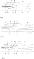
- Each arc extinguishing chamber comprises a
housing 10 and a contact arrangement comprising twocontact members housing 10 and can be moved relative to each other along an axis A. As shown infig. 1 a mechanical drive D can move thecontact member 20 along the axis A, whereas thecontact member 30 is mounted stationary. - The housing comprises a hollow
cylindrical insulator 11 which on its left end supports ahollow metal body 12 and on its right end ahollow metal body 13. Thehollow body 12 resp. 13 surrounds thecontact member 20 resp. 30. Furthermore thehollow metal body 12 resp. 13 is electrical conductively connected to thecontact member 20 resp. 30 and serve as one of the two current terminals of the contact assembly. Ends of themetal bodies insulator 11 which during an opening or closing operation has to withstand a strong dielectric stress. In the embodiment according tofig.1 the switching device is a dead tank breaker and thus comprises a gas-filled metal case which is connected to ground (not shown infig.1 ). The metal case encloses thehousing 10 in a gas-tight manner and receives exhaust gases which escape thehousing 10 when the switching device breaks a current. Thus the before-mentioned ends of thehollow metal bodies hollow shields contact members shields - The two
contact members contact member 20 resp. 30 comprises anarcing contact 21 resp. 31 and anominal contact 22 resp. 32 which surrounds thecorresponding arcing contact 21 resp. 31 coaxially. The arcingcontact 21 is designed as a contact tulip and comprises a plurality of contact fingers which can be arranged in a finger cage or which can be cut in a suitable sleeve. Thecontact tulip 21 and thenominal contact 22 in an electrical conducting manner are fixedly secured to a cylindrically designedcontact carrier 23 of thecontact member 20. A slidingcontact 16 supported on thehollow metal body 12 in a current conducting manner connects thebody 12 to thecontact carrier 23 resp. to the arcing 21 resp. to thenominal contact 22. The arcingcontact 31 is rod-shaped in this embodiment, but can also be designed as a contact tulip. The arcingcontact 31 and thenominal contact 32 are in an electrical conducting manner connected to thehollow metal body 13. If required the arcingcontact 31 can be arranged such that it can be moved axially within thestationary contact member 30. - The
housing 10 further encloses anauxiliary nozzle 40 and a main insulatingnozzle 50 which partly encloses the auxiliary nozzle. Both nozzles are manufactured of a halogenated polymer, typically on the basis of a polytetrafluorethylene (PTFE). Bothnozzles contact carrier 23 and are kept in coaxial arrangement between thecontact tulip 21 lying inside and the hollownominal contact 22 lying outside. Theauxiliary nozzle 40 surrounds thecontact tulip 21 and protrudes beyond the free end of the same. Theauxiliary nozzle 40 and the surroundingmain nozzle 50 border anannular heating channel 61 which connects an arcing zone to aheating volume 60 or to a puffer chamber. - In the closed position of the circuit breaker (shown in
fig.1 above the axis A) the twocontact members contact tulip 21 receives a head of the arcingcontact 31 which is shaped as a plug. - In order to break a current the
contact members nominal contacts contacts contacts contact tulip 21 and the head of the plug-shaped arcing contact 22 (shown infig. 1 below the axis). The arc S generates pressurized arcing gases which viaheating channel 61 flow into theheating volume 60 in which they are stored as arc extinguishing gas. As soon as the plug head of the arcingcontact 31 releases theheating channel 61 the stored arc extinguishing gas - where necessary additionally pressurized by means of a puffer device - passes the arcing zone and afterwards athroat 45 of theauxiliary nozzle 40 as arc extinguishing gas flow P (only shown infig.2 ) and blows the arc S beyond current zero until the current is interrupted. - At current zero the current is interrupted and charge carriers which the switching arc S had generated are widely removed from the gap T. After the interruption of the current the recovery voltage is applied to the gap T and stresses the gap and the
nozzles contact tulip 21 increases the dielectric stress considerably and thus reduce the dielectric recovery of the switching device. A root of the switching arc S favors the erosion and thus the formation of undesired craters and peaks.in the surface of thecontact tulip 21. -
Figures 2 and3 show an embodiment of theauxiliary nozzle 40 which considerably amends the dielectric recovery of the switching device according to the invention. The auxiliary nozzle in coaxial arrangement comprises an insulatingbody 41 and atubular shield 42 which protrudes along the axis A beyond a free end of thecontact tulip 21. Theshield 42 is electrically connected to thecontact tulip 21 and is integrated in an electrical circuit which comprises a current limiter and which extends from a section of theshield 42, which protrudes the free end of thecontact tulip 21, across the current limiter to an end of thecontact tulip 21 which is arranged opposite its free end. Theshield 42 is part of theauxiliary nozzle 40 and surrounds - as shown infig.2 - thecontact tulip 21 and thus also damages caused by arc erosion, like craters and peaks on the surface of thecontact tulip 21. Thus thecontact tulip 21 is screened radially but also axially very effectively. Unavoidable wear of thecontact tulip 21 no more decreases the dielectric recovery of the switching - device. Thus a minimum size of the gap T, which ensures a safe breaking of the current, can be achieved without additional safety measures, like a high relative velocity of the
contact tulip 21 and thearcing contact 31 during current breaking and/or like a maximum size of thecontact tulip 21. Usually the thickness of theshield 42 is only a few 100 µm. For reason of its small thickness and its arrangement in theauxiliary nozzle 40 the space requirements of theshield 42 are negligible. Thus theauxiliary nozzle 40 can replace the auxiliary nozzle of a switching device according to prior art and thus can improve the dielectric recovery of the switching device without any additional place requirements. - The
auxiliary nozzle 40 of the switching device according tofigures 1 and 2 comprises ametallic shield 42. The electrical connection between theshield 42 and thecontact tulip 21 forms the current limiter. The current limiter can be configured as aresistor 43 resp. 44. - The
resistor 43 is configured as a section of the insulatingbody 41 and then can be supported on thecarrier 23 of the contact tulip 21 (embodiment according tofig.2 above the axis A). An end of theresistor 43 then forms acurrent terminal 47 of theshield 42 which ensures that theshield 42 and theresistor 43 are electrically connected to thecontact carrier 23 and thus to thecontact tulip 21. - The
resistor 44 is configured as a resistor modul and is set in an electrically conducting manner on an end of the insulatingbody 41 and is supported on thecarrier 23 of the contact tulip 21 (embodiment according tofig.2 below the axis A). The end of theresistor 44 which is positioned on thecontact carrier 23 forms thecurrent terminal 47 of theshield 42 which ensures that theshield 42 and theresistor 44 are electrically connected to thecontact carrier 23 and thus to thecontact tulip 21. - Each
resistor 43 resp. 44 comprises an electrically conducting polymer, in particular a PTFE having a specific resistance of at least 0,3 Ωm, and limits a current through theshield 42 which can be fed during current breaking with charge carriers generated from the switching arc S. - The
shield 42 is arranged on an internal surface of the insulatingbody 41 and preferably starts downstream athroat 45 of the auxiliary nozzle, which the arc extinguishing gas flow P passes, that means on a conically enlarging portion of theauxiliary nozzle 40. Theshield 42 extends downstream to theresistor 44 resp. to a tubular portion of the insulatingbody 23 which comprises theresistor 43. Theresistor 43 resp. 44 is integrated in an electrical circuit which extends from theshield 42 to an end of thecontact tulip 21 which is arranged opposite its arc-exposed free end. The design of the electrical circuit and theresistor 43 resp. 44 ensure that the root of the switching arc S is kept away resp. is quickly removed from theshield 42 and is kept on the free end or within the interior of the contact tulip. - Halogenated polymers, like PTFE, comprise an anti-adhesive surface. Thus a portion of the internal surface of the insulating
body 42 which holds theshield 42 comprises a roughened and adhesive surface structure. Such a structure can be manufactured using a known reduction method in which the a portion of the anti-adhesive surface of the PTFE is etched with a reducing agent, in particular an alkali metal, like natrium. The reducing agent is applied to the anti-adhesive surface of the insulatingbody 42 either as vapour (US 4,885,018 A ), as solution (US 5,874,154 A ) or as solid (US 2011/0236567 A1 ). The roughened, anti-adhesive surface can be coated currentless with copper and then forms aconductive layer 42a. The conductive layer is shown infig.3 and can be used asshield 42. In order to improve the electrical and mechanical properties of such an embodiment of theshield 42 an additionalconductive layer 42b can be deposited in an electroplating process, in which for example an additional copper layer with a thickness of a few 100 µm can be deposited from an acid copper solution. - The
conductive layer 42a can also be manufactured in a spray or paint process in which a lacquer comprising a metal or semiconductor, like a lubricant on the basis of MoS2, is deposited as a layer on the internal surface of the insulatingbody 41. After drying theconductive layer 42a can be used asshield 42. In order to improve the electrical and mechanical properties of such a shield an additionalconductive layer 42b can be deposited in an electroplating process on thelayer 42a. Furthermore the additionalconductive layer 42b can be configured as tubular sleeve of a metallic or semiconductive material which is plugged in the insulatingbody 41 and which contacts thelayer 42a in order to keep thesleeve 42b on the potential of theconductive layer 42a. - In order to protect the
shield 42 against the switching arc S an insulatinglayer 46 is applied to theshield 42. Thelayer 46 typically comprises a halogenated polymer, like PTFE, and can be deposited in a sputtering process as described inUS 2011/0236567 A1 . The protection can also be achieved with an insulating sleeve which is plugged in the insulatingbody 41 and which covers theshield 42 instead of or additional to the insulatinglayer 46. The thickness of the insulatinglayer 46 resp. of the insulating sleeve can be some millimeters, typically 1 to 5 millimeters. - In contrast to the embodiment according to
figures 2 and3 theadditional conducting layer 42b of the embodiment according tofig. 4 comprises a semiconductive hollowcylindrical insert 70 made of an electrically conductive halogenated polymer, preferably a PTFE filled with an electrically conducting powder, like carbon black. Anannular section 71 of theinsert 70 which protrudes the free end of the contact tulip 21 (shown infig. 1 ) fills arecess 72 cut in the insulatingbody 41. Thesection 71 is configured in a manner to form together with the stationaryhollow shield 14 and the nominal contact 22 (only shown infig.1 ) an equipotential surface which in the open position of the switching device is largely spherical. In order to facilitate the manufacture of theauxiliary nozzle 40 two undercuts of therecess 72 are each filled with an electrical conductingannular part 73 resp. 74 of theshield section 71 in a manner to form a recess with coaxially arranged and axially extended faces 75, 76. Theparts layer 42a and each comprise a convex profile which is designed in a manner to improve the screen function of theinsert 70. The conducting layer 41a covers therecess 72 and electrically contacts theinsert 70 when in a manufacturing process theinsert 70 is plugged in the recess comprising thefaces additional conducting layer 42b can be some millimeters, typically 1 to 5 millimeters. -
Fig. 5 and the following figures show sectional views of further embodiments of the switching device according to the invention. Also these embodiments of the switching device are rotationally symmetric around the longitudinal axis A and only an upper half of the sectional views is shown. Only the elements of the switching devices, in the following referred to as circuit breakers, which are related to the present invention will be described in the following, whereas other elements, e.g. nominal contacts, enclosure, etc. are not shown in the figures. - The
contact tulip 21 comprises multiple fingers arranged in a finger cage. The arcingcontact 31 is rod-shaped in this embodiment. For the sake of simplicity, only one finger of thecontact tulip 21 shown inFig. 5 and the following figures. - The
auxiliary nozzle 40 is arranged partly around thecontact tulip 21. In other words, theauxiliary nozzle 40 encloses thecontact tulip 21 concentrically and protrudes beyond it, as can be seen in the figure. Accordingly, the arcingcontact 31 is enclosed by themain nozzle 50, which partly encloses theauxiliary nozzle 40. A purpose of theauxiliary nozzle 40 and themain nozzle 50 is to form a path, here theheating channel 61, for guiding the insulating fluid into and out of the before-described arcing zone Z, which infig.6 and the following figures is denoted with the reference numeral Z. - In other words, the arcing
contact 31 is enclosed by themain nozzle 50, which partly encloses theauxiliary nozzle 40 such that theheating channel 61 is formed between themain nozzle 50 and theauxiliary nozzle 40, which channel 61 fluidly connects the arcing zone Z of the circuit breaker with theheating volume 60 resp. a puffer chamber of the switching device. - As mentioned analogously before the arcing zone Z is a region in which the
contact tulip 21 is moved back and forth for closing or opening the circuit breaker and in which the switching arc S develops betweencontact tulip 21 and thearcing contact 31 during an opening and closing procedure, thereby heating up the fluid located in the arcing zone Z. - The
auxiliary nozzle 40 comprises inside its body theshield 42. Theshield 42 is electrically connected to thecontact tulip 21. The material of theshield 42 is conductive or is semiconductive. Particularly, the shield is made of a material which is similar to the surroundingauxiliary nozzle 40, which typically is made of a PTFE. An appropriate material is a PTFE- carbon compound. This has the advantage that thesemiconducting shield 42 has similar mechanical properties like the surrounding material of theauxiliary nozzle 40. - In this embodiment, the
shield 42 is fixedly embedded in the body of theauxiliary nozzle 40 and is entirely enclosed by theauxiliary nozzle 40. However, in another embodiment theshield 42 is a distinct element insertable into the body of theauxiliary nozzle 40. - The
shield 40 is electrically connected to thecontact tulip 21 by a semiconductor ceramic ormetal connection 48 having a predefined electrical resistance and acting as the afore-described current limiter. - The shape of the
shield 42 is shown only exemplarily inFig. 5 . It is chosen depending on the dimensions of theauxiliary nozzle 40 and is chosen in such a way that electric field stresses are minimal. - Depending on its shape, the
shield 42 may be inserted into theauxiliary nozzle 40 as an independent element or it may form a part of theauxiliary nozzle 40, as mentioned above. In the second case theshield 42 may be manufactured first and theauxiliary nozzle 40 may be formed around it in known ways, e.g. by injection moulding of polytetrafluoroethylene. - Preferably, the
shield 42 is elongated with respect to the axis A, and in particular has a tubular or substantially tubular shape concentric to the axis. By using ashield 42 with said shape the shielding of thecontact tulip 21 is improved and thus the electrical field strength on the side of thecontact tulip 42 does not depend on the condition of its surface. Instead, the electrical field strength on the side of the contact tulip is given by the electrical field strength of theshield 42. - Different to the embodiment according to
fig.5 in the embodiment according tofig.6 theauxiliary nozzle 40 comprises ashield 42 which is adjacent to theheating channel 61 and which consists of ablation-resistant material. The term "ablation-resistant" is understood as referring to a material exhibiting a minimum mechanical ablation in the presence of a switching arc, as compared to other available conductive or semiconducting materials, particularly as compared to nozzles made of PTFE. It encompasses also non-ablating materials. Theshield 42 is electrically connected to thecontact tulip 21. The material of theshield 42 is conductive or semi-conductive. Particularly, the material of the shield comprises metal, e.g. tungsten or wolfram or steel, and/or a ceramic semiconductor. It may also comprise or be made of PTFE with an appropriate filler. In this embodiment theshield 42 is only formed by the front part of theauxiliary nozzle 40. The rest of theauxiliary nozzle 40 comprises the insulatingbody 41, usually PTFE. - The
shield 42 is electrically connected to thecontact tulip 21 by a semiconductor ceramic ormetal connection 48. In this embodiment theconnection 48 is formed by a line embedded in the insulatingbody 41. - Different to the embodiment according to
fig.6 theauxiliary nozzle 40 of the embodiment according tofig.7 is made of ablation-resistant material. In this case the material comprises a semiconducting ceramic and/or a metal, which ensure the ablation-resistance and the limitation of a possible current from theauxiliary nozzle 40 to an end of thecontact tulip 21 which is opposite its free shielded end. Theconnection 48 between theauxiliary nozzle 40 and thecontact tulip 21 is made of metal or ceramic. - In both cases the semiconductor ceramic or
metal connection 48 is dimensioned to have a pre-defined electrical resistance in order to avoid high current flow through theauxiliary nozzle 40. For example, TIG-welding processed ceramic material can be used for thisconnection 48. -
Fig. 8 shows yet another embodiment of the switching device according to the invention. This embodiment only differs from the embodiment according tofig.7 in that theshield 42 is formed by the free end of theauxiliary nozzle 40 and is separated from theheating channel 61 by the insulating material of thebody 41. - While there are shown and described presently preferred embodiments of the invention, it is to be distinctly understood that the invention is not limited thereto but may otherwise variously be embodied and practised within the scope of the following claims. Therefore, terms like "preferred" or "in particular" or "particularly" or "advantageously", etc. signify optional and exemplary embodiments only.
- The electrical switching device is preferably used as an earthing device, a fast-acting earthing device, a circuit breaker, a generator circuit breaker, a disconnector, a combined disconnector and earthing switch, or a load break switch.
-
- 10
- housing
- 11
- hollow cylindrical insulator
- 12, 13
- hollow metal bodies,
- 14, 15
- hollow shields,
- 16
- sliding contact,
- 20
- contact member
- 21
- arcing contact, contact tulip
- 22
- nominal contact
- 23
- contact carrier
- 30
- contact member
- 31
- arcing contact
- 32
- nominal contact
- 40
- auxiliary nozzle
- 41
- insulating body
- 42
- shield
- 42a, 42b
- conductive layers
- 43, 44
- resistors
- 45
- throat
- 46
- insulating layer
- 47
- current terminal
- 48
- electrical connection
- 50
- main insulating nozzle
- 60
- heating volume
- 61
- heating channel
- 70
- semiconductive hollow cylindrical insert
- 71
- annular section of the
shield 42 - 72
- recess
- 73, 74
- parts of the
annular section 71 - 75, 76
- axially extended faces of a recess
- A
- axis
- D
- drive
- P
- arc extinguishing arc flow
- S
- switching arc
- T
- gap
- Z
- arcing zone
Claims (17)
- A gas-insulated high voltage switching device with a contact arrangement extended along an axis (A) comprising:a first arcing contact designed as a contact tulip (21) and a second arcing contact (31),an auxiliary nozzle (40) enclosing at least partially the contact tulip (21),a main insulating nozzle (50) enclosing at least partially the auxiliary nozzle (40) such that a heating channel (61) is formed between the auxiliary (40) and the main insulating nozzle (50), anda tubular electrostatic shield (42) which protrudes along the axis (A) beyond a free end of the contact tulip (21),characterized in that the shield (42) is electrically connected to the contact tulip (21) and is integrated in an electrical circuit comprising a current limiter and extending from the shield (42) through the current limiter to an end of the contact tulip (21) which is arranged opposite its free end.
- The switching device according to claim 1, wherein at least a section of the electrical circuit forms the current limiter.
- The switching device according to claim 2, wherein the current limiter comprises a semi-conductive material.
- The switching device according to claim 3, wherein the specific resistance of the semi-conductive material is at least 0,3 [kΩ·m].
- The switching device according to one of claims 2 to 4, wherein the shield (42) is metallic, and wherein an electrical connection (48) between the shield (42) and the contact tulip (21) forms the current limiter.
- The switching device according to one of claims 1 to claim 5, wherein the auxiliary nozzle (40) in coaxial arrangement comprises an insulating body (41) and the tubular electrostatic shield (42).
- The switching device according to claim 6, wherein the current limiter is a resistor (43) which is configured as a section of the insulating body (41) and which is supported on a carrier (23) of the contact tulip (21).
- The switching device according to claim 6, wherein the current limiter is a resistor (44) which is attached to the insulating body (41) and which is supported on a carrier (23) of the contact tulip (21).
- The switching device according to one of claims 6 to 8, wherein the shield (42) is entirely enclosed in the insulating body (41).
- The switching device according to one of claims 6 to 9, wherein the material of the insulating body (41) is a halogenated polymeric material, and wherein the shield (42) is arranged on an internal surface of the insulating body (41) and preferably starts downstream a throat (45) on a conically enlarging portion of the auxiliary nozzle (40) and extends downstream to a tubular portion of the insulating body (41).
- The switching device according to claim 10, wherein the shield (42) comprises a conductive layer (42a) which is applied to the internal surface and which either comprises a sprayed conductivity lacquer or a metallic material being deposited on the afore-etched internal surface.
- The switching device according to claim 11, wherein the shield (42) further comprises a tubular body (42b) of a metallic or semiconductive material which is kept on the potential of the conductive layer (42a), and which is deposited electrochemically or mechanically on the conductive layer (42a) or which is plugged in the insulating body (41).
- The switching device according to claim 12, wherein the tubular body (42b) comprises a semiconductive hollow cylindrical insert (70) which is plugged in an annular recess (72) of the insulating body (41), and wherein preferably an electrically conducting annular part (73, 74) of the shield (42) fills an undercut of the recess (72).
- The switching device according to one of claims 6 to 13, wherein an insulating coating (46) is applied to the shield (42) and/or wherein an insulating sleeve is plugged in the insulating body (41).
- The switching device according to one of claims 6 to 14, wherein the shield (42) is formed as a free end of the auxiliary nozzle (40) and wherein the free end is adjacent to the heating channel (61) or is separated from the heating channel (61) by an external portion of the insulating body (41).
- The switching device according to claim 15, wherein at least the shield (42) is made of ablation-resistant material.
- An auxiliary nozzle (40) for the gas-insulated high voltage switching device according to one claims 6 to 16, wherein the auxiliary nozzle (40) in coaxial arrangement comprises the insulating body (41), the tubular electrostatic shield (42) and the current limiter, and
wherein the auxiliary nozzle (40) further comprises a terminal (47) for electrically connecting the electrostatic shield (42) to an end of the contact tulip (21) which is opposite its free end.
Applications Claiming Priority (3)
| Application Number | Priority Date | Filing Date | Title |
|---|---|---|---|
| EP14164783 | 2014-04-15 | ||
| EP14191750 | 2014-11-04 | ||
| PCT/EP2015/057018 WO2015158544A1 (en) | 2014-04-15 | 2015-03-31 | High voltage switching device with auxiliary nozzle |
Publications (2)
| Publication Number | Publication Date |
|---|---|
| EP3132461A1 EP3132461A1 (en) | 2017-02-22 |
| EP3132461B1 true EP3132461B1 (en) | 2017-12-13 |
Family
ID=53724268
Family Applications (1)
| Application Number | Title | Priority Date | Filing Date |
|---|---|---|---|
| EP15741875.7A Active EP3132461B1 (en) | 2014-04-15 | 2015-03-31 | High voltage switching device with auxiliary nozzle |
Country Status (2)
| Country | Link |
|---|---|
| EP (1) | EP3132461B1 (en) |
| WO (1) | WO2015158544A1 (en) |
Family Cites Families (8)
| Publication number | Priority date | Publication date | Assignee | Title |
|---|---|---|---|---|
| FR2057344A5 (en) * | 1969-08-12 | 1971-05-21 | Merlin Gerin | |
| CH652528A5 (en) * | 1980-10-31 | 1985-11-15 | Bbc Brown Boveri & Cie | EXHAUST GAS SWITCH. |
| EP0081253A1 (en) | 1981-12-03 | 1983-06-15 | BBC Aktiengesellschaft Brown, Boveri & Cie. | Gas blast switch |
| DE3702025A1 (en) | 1987-01-24 | 1988-08-04 | Philips Patentverwaltung | METHOD AND DEVICE FOR PRODUCING ROTATIONALLY SYMMETRIC POROESE SOLID BODIES |
| JP2524436B2 (en) | 1990-09-18 | 1996-08-14 | インターナショナル・ビジネス・マシーンズ・コーポレイション | Surface treatment method |
| ATE352853T1 (en) | 2003-12-19 | 2007-02-15 | Abb Technology Ag | GAS-INSULATED SWITCHING DEVICE WITH A NOZZLE |
| ES2351844T3 (en) | 2005-10-10 | 2011-02-11 | Abb Research Ltd. | ESTIMATION OF PARAMETERS FOR ELECTRICAL NETWORKS. |
| US20110236567A1 (en) | 2010-03-26 | 2011-09-29 | Semiconductor Energy Laboratory Co., Ltd. | Method of forming electrode |
-
2015
- 2015-03-31 EP EP15741875.7A patent/EP3132461B1/en active Active
- 2015-03-31 WO PCT/EP2015/057018 patent/WO2015158544A1/en active Application Filing
Also Published As
| Publication number | Publication date |
|---|---|
| EP3132461A1 (en) | 2017-02-22 |
| WO2015158544A1 (en) | 2015-10-22 |
Similar Documents
| Publication | Publication Date | Title |
|---|---|---|
| US5981893A (en) | Electrical switching device | |
| EP3433870B1 (en) | Electrical circuit breaker device with particle trap | |
| WO2015039918A1 (en) | High-voltage circuit breaker with improved robustness | |
| EP2346061A1 (en) | Electrode structure for vacuum circuit breaker | |
| US4841108A (en) | Recloser plenum puffer interrupter | |
| US8901447B2 (en) | Circuit breaker with parallel rated current paths | |
| EP3132461B1 (en) | High voltage switching device with auxiliary nozzle | |
| EP2369608B1 (en) | High-voltage circuit breaker | |
| WO2014122084A1 (en) | Contact arrangement and electrical switching device with such contact arrangement | |
| US20230420203A1 (en) | Electrical switching device | |
| US11062862B2 (en) | Gas-insulated high or medium voltage circuit breaker | |
| JP4131926B2 (en) | Gas circuit breaker | |
| US10699862B2 (en) | Gas-insulated high-voltage switching device with improved main nozzle | |
| US20080135523A1 (en) | Self-blast circuit breaker with control body | |
| EP3433869B1 (en) | Electrical circuit breaker device | |
| US7679021B2 (en) | Switching device | |
| US20140174895A1 (en) | Contact arrangement for high voltage switchgear with contact arrangement | |
| EP4141901A1 (en) | Metal enclosed circuit breaker | |
| CN110402475B (en) | High-voltage circuit breaker with improved robustness | |
| EP3926654B1 (en) | Circuit breaker with field deflection element | |
| JP7200084B2 (en) | gas circuit breaker | |
| EP2827353A1 (en) | Electrical switching device | |
| JP2010061858A (en) | Gas-blast circuit breaker | |
| JP3307099B2 (en) | Gas switch | |
| CN117616528A (en) | Gas-insulated high-voltage or medium-voltage circuit breaker |
Legal Events
| Date | Code | Title | Description |
|---|---|---|---|
| STAA | Information on the status of an ep patent application or granted ep patent |
Free format text: STATUS: THE INTERNATIONAL PUBLICATION HAS BEEN MADE |
|
| PUAI | Public reference made under article 153(3) epc to a published international application that has entered the european phase |
Free format text: ORIGINAL CODE: 0009012 |
|
| STAA | Information on the status of an ep patent application or granted ep patent |
Free format text: STATUS: REQUEST FOR EXAMINATION WAS MADE |
|
| 17P | Request for examination filed |
Effective date: 20161003 |
|
| AK | Designated contracting states |
Kind code of ref document: A1 Designated state(s): AL AT BE BG CH CY CZ DE DK EE ES FI FR GB GR HR HU IE IS IT LI LT LU LV MC MK MT NL NO PL PT RO RS SE SI SK SM TR |
|
| AX | Request for extension of the european patent |
Extension state: BA ME |
|
| RIN1 | Information on inventor provided before grant (corrected) |
Inventor name: ANDRAE, GUNNAR Inventor name: GALLETTI, BERNARDO Inventor name: COSTYSON, JOHAN Inventor name: KOTILAINEN, SAMI Inventor name: KOSTOVIC, JADRAN Inventor name: DHOTRE, MAHESH Inventor name: YE, XIANGYANG Inventor name: HEIERMEIER, HELMUT Inventor name: LUNDQVIST, FREDRIK Inventor name: SUTHERLAND, TIMOTHY |
|
| DAV | Request for validation of the european patent (deleted) | ||
| DAX | Request for extension of the european patent (deleted) | ||
| GRAP | Despatch of communication of intention to grant a patent |
Free format text: ORIGINAL CODE: EPIDOSNIGR1 |
|
| STAA | Information on the status of an ep patent application or granted ep patent |
Free format text: STATUS: GRANT OF PATENT IS INTENDED |
|
| INTG | Intention to grant announced |
Effective date: 20170818 |
|
| GRAS | Grant fee paid |
Free format text: ORIGINAL CODE: EPIDOSNIGR3 |
|
| GRAA | (expected) grant |
Free format text: ORIGINAL CODE: 0009210 |
|
| STAA | Information on the status of an ep patent application or granted ep patent |
Free format text: STATUS: THE PATENT HAS BEEN GRANTED |
|
| REG | Reference to a national code |
Ref country code: GB Ref legal event code: FG4D |
|
| REG | Reference to a national code |
Ref country code: AT Ref legal event code: REF Ref document number: 955126 Country of ref document: AT Kind code of ref document: T Effective date: 20171215 Ref country code: CH Ref legal event code: EP |
|
| REG | Reference to a national code |
Ref country code: IE Ref legal event code: FG4D |
|
| REG | Reference to a national code |
Ref country code: DE Ref legal event code: R096 Ref document number: 602015006699 Country of ref document: DE |
|
| REG | Reference to a national code |
Ref country code: FR Ref legal event code: PLFP Year of fee payment: 4 |
|
| REG | Reference to a national code |
Ref country code: NL Ref legal event code: MP Effective date: 20171213 |
|
| PG25 | Lapsed in a contracting state [announced via postgrant information from national office to epo] |
Ref country code: FI Free format text: LAPSE BECAUSE OF FAILURE TO SUBMIT A TRANSLATION OF THE DESCRIPTION OR TO PAY THE FEE WITHIN THE PRESCRIBED TIME-LIMIT Effective date: 20171213 Ref country code: SE Free format text: LAPSE BECAUSE OF FAILURE TO SUBMIT A TRANSLATION OF THE DESCRIPTION OR TO PAY THE FEE WITHIN THE PRESCRIBED TIME-LIMIT Effective date: 20171213 Ref country code: NO Free format text: LAPSE BECAUSE OF FAILURE TO SUBMIT A TRANSLATION OF THE DESCRIPTION OR TO PAY THE FEE WITHIN THE PRESCRIBED TIME-LIMIT Effective date: 20180313 |
|
| REG | Reference to a national code |
Ref country code: AT Ref legal event code: MK05 Ref document number: 955126 Country of ref document: AT Kind code of ref document: T Effective date: 20171213 |
|
| PG25 | Lapsed in a contracting state [announced via postgrant information from national office to epo] |
Ref country code: RS Free format text: LAPSE BECAUSE OF FAILURE TO SUBMIT A TRANSLATION OF THE DESCRIPTION OR TO PAY THE FEE WITHIN THE PRESCRIBED TIME-LIMIT Effective date: 20171213 Ref country code: BG Free format text: LAPSE BECAUSE OF FAILURE TO SUBMIT A TRANSLATION OF THE DESCRIPTION OR TO PAY THE FEE WITHIN THE PRESCRIBED TIME-LIMIT Effective date: 20180313 Ref country code: LV Free format text: LAPSE BECAUSE OF FAILURE TO SUBMIT A TRANSLATION OF THE DESCRIPTION OR TO PAY THE FEE WITHIN THE PRESCRIBED TIME-LIMIT Effective date: 20171213 Ref country code: GR Free format text: LAPSE BECAUSE OF FAILURE TO SUBMIT A TRANSLATION OF THE DESCRIPTION OR TO PAY THE FEE WITHIN THE PRESCRIBED TIME-LIMIT Effective date: 20180314 Ref country code: HR Free format text: LAPSE BECAUSE OF FAILURE TO SUBMIT A TRANSLATION OF THE DESCRIPTION OR TO PAY THE FEE WITHIN THE PRESCRIBED TIME-LIMIT Effective date: 20171213 |
|
| PG25 | Lapsed in a contracting state [announced via postgrant information from national office to epo] |
Ref country code: NL Free format text: LAPSE BECAUSE OF FAILURE TO SUBMIT A TRANSLATION OF THE DESCRIPTION OR TO PAY THE FEE WITHIN THE PRESCRIBED TIME-LIMIT Effective date: 20171213 |
|
| PG25 | Lapsed in a contracting state [announced via postgrant information from national office to epo] |
Ref country code: CZ Free format text: LAPSE BECAUSE OF FAILURE TO SUBMIT A TRANSLATION OF THE DESCRIPTION OR TO PAY THE FEE WITHIN THE PRESCRIBED TIME-LIMIT Effective date: 20171213 Ref country code: ES Free format text: LAPSE BECAUSE OF FAILURE TO SUBMIT A TRANSLATION OF THE DESCRIPTION OR TO PAY THE FEE WITHIN THE PRESCRIBED TIME-LIMIT Effective date: 20171213 Ref country code: CY Free format text: LAPSE BECAUSE OF FAILURE TO SUBMIT A TRANSLATION OF THE DESCRIPTION OR TO PAY THE FEE WITHIN THE PRESCRIBED TIME-LIMIT Effective date: 20171213 Ref country code: EE Free format text: LAPSE BECAUSE OF FAILURE TO SUBMIT A TRANSLATION OF THE DESCRIPTION OR TO PAY THE FEE WITHIN THE PRESCRIBED TIME-LIMIT Effective date: 20171213 Ref country code: SK Free format text: LAPSE BECAUSE OF FAILURE TO SUBMIT A TRANSLATION OF THE DESCRIPTION OR TO PAY THE FEE WITHIN THE PRESCRIBED TIME-LIMIT Effective date: 20171213 |
|
| PG25 | Lapsed in a contracting state [announced via postgrant information from national office to epo] |
Ref country code: IS Free format text: LAPSE BECAUSE OF FAILURE TO SUBMIT A TRANSLATION OF THE DESCRIPTION OR TO PAY THE FEE WITHIN THE PRESCRIBED TIME-LIMIT Effective date: 20180413 Ref country code: PL Free format text: LAPSE BECAUSE OF FAILURE TO SUBMIT A TRANSLATION OF THE DESCRIPTION OR TO PAY THE FEE WITHIN THE PRESCRIBED TIME-LIMIT Effective date: 20171213 Ref country code: AT Free format text: LAPSE BECAUSE OF FAILURE TO SUBMIT A TRANSLATION OF THE DESCRIPTION OR TO PAY THE FEE WITHIN THE PRESCRIBED TIME-LIMIT Effective date: 20171213 Ref country code: SM Free format text: LAPSE BECAUSE OF FAILURE TO SUBMIT A TRANSLATION OF THE DESCRIPTION OR TO PAY THE FEE WITHIN THE PRESCRIBED TIME-LIMIT Effective date: 20171213 Ref country code: IT Free format text: LAPSE BECAUSE OF FAILURE TO SUBMIT A TRANSLATION OF THE DESCRIPTION OR TO PAY THE FEE WITHIN THE PRESCRIBED TIME-LIMIT Effective date: 20171213 |
|
| REG | Reference to a national code |
Ref country code: DE Ref legal event code: R097 Ref document number: 602015006699 Country of ref document: DE |
|
| PLBE | No opposition filed within time limit |
Free format text: ORIGINAL CODE: 0009261 |
|
| STAA | Information on the status of an ep patent application or granted ep patent |
Free format text: STATUS: NO OPPOSITION FILED WITHIN TIME LIMIT |
|
| REG | Reference to a national code |
Ref country code: CH Ref legal event code: PL |
|
| 26N | No opposition filed |
Effective date: 20180914 |
|
| PG25 | Lapsed in a contracting state [announced via postgrant information from national office to epo] |
Ref country code: DK Free format text: LAPSE BECAUSE OF FAILURE TO SUBMIT A TRANSLATION OF THE DESCRIPTION OR TO PAY THE FEE WITHIN THE PRESCRIBED TIME-LIMIT Effective date: 20171213 Ref country code: MC Free format text: LAPSE BECAUSE OF FAILURE TO SUBMIT A TRANSLATION OF THE DESCRIPTION OR TO PAY THE FEE WITHIN THE PRESCRIBED TIME-LIMIT Effective date: 20171213 |
|
| REG | Reference to a national code |
Ref country code: BE Ref legal event code: MM Effective date: 20180331 |
|
| REG | Reference to a national code |
Ref country code: IE Ref legal event code: MM4A |
|
| PG25 | Lapsed in a contracting state [announced via postgrant information from national office to epo] |
Ref country code: LU Free format text: LAPSE BECAUSE OF NON-PAYMENT OF DUE FEES Effective date: 20180331 |
|
| PG25 | Lapsed in a contracting state [announced via postgrant information from national office to epo] |
Ref country code: IE Free format text: LAPSE BECAUSE OF NON-PAYMENT OF DUE FEES Effective date: 20180331 |
|
| PG25 | Lapsed in a contracting state [announced via postgrant information from national office to epo] |
Ref country code: SI Free format text: LAPSE BECAUSE OF FAILURE TO SUBMIT A TRANSLATION OF THE DESCRIPTION OR TO PAY THE FEE WITHIN THE PRESCRIBED TIME-LIMIT Effective date: 20171213 Ref country code: CH Free format text: LAPSE BECAUSE OF NON-PAYMENT OF DUE FEES Effective date: 20180331 Ref country code: BE Free format text: LAPSE BECAUSE OF NON-PAYMENT OF DUE FEES Effective date: 20180331 Ref country code: LI Free format text: LAPSE BECAUSE OF NON-PAYMENT OF DUE FEES Effective date: 20180331 |
|
| GBPC | Gb: european patent ceased through non-payment of renewal fee |
Effective date: 20190331 |
|
| PG25 | Lapsed in a contracting state [announced via postgrant information from national office to epo] |
Ref country code: MT Free format text: LAPSE BECAUSE OF NON-PAYMENT OF DUE FEES Effective date: 20180331 Ref country code: GB Free format text: LAPSE BECAUSE OF NON-PAYMENT OF DUE FEES Effective date: 20190331 |
|
| PG25 | Lapsed in a contracting state [announced via postgrant information from national office to epo] |
Ref country code: TR Free format text: LAPSE BECAUSE OF FAILURE TO SUBMIT A TRANSLATION OF THE DESCRIPTION OR TO PAY THE FEE WITHIN THE PRESCRIBED TIME-LIMIT Effective date: 20171213 |
|
| PG25 | Lapsed in a contracting state [announced via postgrant information from national office to epo] |
Ref country code: PT Free format text: LAPSE BECAUSE OF FAILURE TO SUBMIT A TRANSLATION OF THE DESCRIPTION OR TO PAY THE FEE WITHIN THE PRESCRIBED TIME-LIMIT Effective date: 20171213 |
|
| PG25 | Lapsed in a contracting state [announced via postgrant information from national office to epo] |
Ref country code: RO Free format text: LAPSE BECAUSE OF FAILURE TO SUBMIT A TRANSLATION OF THE DESCRIPTION OR TO PAY THE FEE WITHIN THE PRESCRIBED TIME-LIMIT Effective date: 20171213 Ref country code: LT Free format text: LAPSE BECAUSE OF FAILURE TO SUBMIT A TRANSLATION OF THE DESCRIPTION OR TO PAY THE FEE WITHIN THE PRESCRIBED TIME-LIMIT Effective date: 20171213 Ref country code: HU Free format text: LAPSE BECAUSE OF FAILURE TO SUBMIT A TRANSLATION OF THE DESCRIPTION OR TO PAY THE FEE WITHIN THE PRESCRIBED TIME-LIMIT; INVALID AB INITIO Effective date: 20150331 Ref country code: MK Free format text: LAPSE BECAUSE OF NON-PAYMENT OF DUE FEES Effective date: 20171213 |
|
| PG25 | Lapsed in a contracting state [announced via postgrant information from national office to epo] |
Ref country code: AL Free format text: LAPSE BECAUSE OF FAILURE TO SUBMIT A TRANSLATION OF THE DESCRIPTION OR TO PAY THE FEE WITHIN THE PRESCRIBED TIME-LIMIT Effective date: 20171213 |
|
| REG | Reference to a national code |
Ref country code: DE Ref legal event code: R081 Ref document number: 602015006699 Country of ref document: DE Owner name: HITACHI ENERGY SWITZERLAND AG, CH Free format text: FORMER OWNER: ABB SCHWEIZ AG, BADEN, CH Ref country code: DE Ref legal event code: R081 Ref document number: 602015006699 Country of ref document: DE Owner name: HITACHI ENERGY LTD, CH Free format text: FORMER OWNER: ABB SCHWEIZ AG, BADEN, CH Ref country code: DE Ref legal event code: R082 Ref document number: 602015006699 Country of ref document: DE Representative=s name: DENNEMEYER & ASSOCIATES S.A., DE Ref country code: DE Ref legal event code: R081 Ref document number: 602015006699 Country of ref document: DE Owner name: ABB POWER GRIDS SWITZERLAND AG, CH Free format text: FORMER OWNER: ABB SCHWEIZ AG, BADEN, CH |
|
| REG | Reference to a national code |
Ref country code: DE Ref legal event code: R081 Ref document number: 602015006699 Country of ref document: DE Owner name: HITACHI ENERGY SWITZERLAND AG, CH Free format text: FORMER OWNER: ABB POWER GRIDS SWITZERLAND AG, BADEN, CH Ref country code: DE Ref legal event code: R081 Ref document number: 602015006699 Country of ref document: DE Owner name: HITACHI ENERGY LTD, CH Free format text: FORMER OWNER: ABB POWER GRIDS SWITZERLAND AG, BADEN, CH |
|
| PGFP | Annual fee paid to national office [announced via postgrant information from national office to epo] |
Ref country code: FR Payment date: 20230324 Year of fee payment: 9 |
|
| PGFP | Annual fee paid to national office [announced via postgrant information from national office to epo] |
Ref country code: DE Payment date: 20230321 Year of fee payment: 9 |
|
| P01 | Opt-out of the competence of the unified patent court (upc) registered |
Effective date: 20230527 |
|
| REG | Reference to a national code |
Ref country code: DE Ref legal event code: R082 Ref document number: 602015006699 Country of ref document: DE Representative=s name: DENNEMEYER & ASSOCIATES S.A., DE Ref country code: DE Ref legal event code: R081 Ref document number: 602015006699 Country of ref document: DE Owner name: HITACHI ENERGY LTD, CH Free format text: FORMER OWNER: HITACHI ENERGY SWITZERLAND AG, BADEN, CH |