EP3131310B1 - System of terminal and earphone capable of reducing noises generated in earphone insertion and pulling processes - Google Patents
System of terminal and earphone capable of reducing noises generated in earphone insertion and pulling processes Download PDFInfo
- Publication number
- EP3131310B1 EP3131310B1 EP14896799.5A EP14896799A EP3131310B1 EP 3131310 B1 EP3131310 B1 EP 3131310B1 EP 14896799 A EP14896799 A EP 14896799A EP 3131310 B1 EP3131310 B1 EP 3131310B1
- Authority
- EP
- European Patent Office
- Prior art keywords
- earphone
- pin
- switch circuit
- terminal
- voltage
- Prior art date
- Legal status (The legal status is an assumption and is not a legal conclusion. Google has not performed a legal analysis and makes no representation as to the accuracy of the status listed.)
- Active
Links
- 238000000034 method Methods 0.000 title claims description 18
- 230000008569 process Effects 0.000 title claims description 16
- 238000003780 insertion Methods 0.000 title 1
- 230000037431 insertion Effects 0.000 title 1
- 238000009413 insulation Methods 0.000 claims description 5
- 238000010586 diagram Methods 0.000 description 13
- 238000013461 design Methods 0.000 description 3
- 230000006870 function Effects 0.000 description 3
- 230000009467 reduction Effects 0.000 description 3
- 238000005516 engineering process Methods 0.000 description 2
- 238000004519 manufacturing process Methods 0.000 description 2
- 230000004048 modification Effects 0.000 description 2
- 238000012986 modification Methods 0.000 description 2
- 239000003990 capacitor Substances 0.000 description 1
- 230000008859 change Effects 0.000 description 1
- 238000001514 detection method Methods 0.000 description 1
- 238000011161 development Methods 0.000 description 1
- 230000006872 improvement Effects 0.000 description 1
Images


Classifications
-
- H—ELECTRICITY
- H04—ELECTRIC COMMUNICATION TECHNIQUE
- H04R—LOUDSPEAKERS, MICROPHONES, GRAMOPHONE PICK-UPS OR LIKE ACOUSTIC ELECTROMECHANICAL TRANSDUCERS; DEAF-AID SETS; PUBLIC ADDRESS SYSTEMS
- H04R5/00—Stereophonic arrangements
- H04R5/04—Circuit arrangements, e.g. for selective connection of amplifier inputs/outputs to loudspeakers, for loudspeaker detection, or for adaptation of settings to personal preferences or hearing impairments
-
- H—ELECTRICITY
- H04—ELECTRIC COMMUNICATION TECHNIQUE
- H04R—LOUDSPEAKERS, MICROPHONES, GRAMOPHONE PICK-UPS OR LIKE ACOUSTIC ELECTROMECHANICAL TRANSDUCERS; DEAF-AID SETS; PUBLIC ADDRESS SYSTEMS
- H04R3/00—Circuits for transducers, loudspeakers or microphones
-
- H—ELECTRICITY
- H04—ELECTRIC COMMUNICATION TECHNIQUE
- H04R—LOUDSPEAKERS, MICROPHONES, GRAMOPHONE PICK-UPS OR LIKE ACOUSTIC ELECTROMECHANICAL TRANSDUCERS; DEAF-AID SETS; PUBLIC ADDRESS SYSTEMS
- H04R29/00—Monitoring arrangements; Testing arrangements
-
- H—ELECTRICITY
- H04—ELECTRIC COMMUNICATION TECHNIQUE
- H04R—LOUDSPEAKERS, MICROPHONES, GRAMOPHONE PICK-UPS OR LIKE ACOUSTIC ELECTROMECHANICAL TRANSDUCERS; DEAF-AID SETS; PUBLIC ADDRESS SYSTEMS
- H04R1/00—Details of transducers, loudspeakers or microphones
- H04R1/10—Earpieces; Attachments therefor ; Earphones; Monophonic headphones
- H04R1/1091—Details not provided for in groups H04R1/1008 - H04R1/1083
-
- H—ELECTRICITY
- H04—ELECTRIC COMMUNICATION TECHNIQUE
- H04R—LOUDSPEAKERS, MICROPHONES, GRAMOPHONE PICK-UPS OR LIKE ACOUSTIC ELECTROMECHANICAL TRANSDUCERS; DEAF-AID SETS; PUBLIC ADDRESS SYSTEMS
- H04R29/00—Monitoring arrangements; Testing arrangements
- H04R29/001—Monitoring arrangements; Testing arrangements for loudspeakers
-
- H—ELECTRICITY
- H04—ELECTRIC COMMUNICATION TECHNIQUE
- H04R—LOUDSPEAKERS, MICROPHONES, GRAMOPHONE PICK-UPS OR LIKE ACOUSTIC ELECTROMECHANICAL TRANSDUCERS; DEAF-AID SETS; PUBLIC ADDRESS SYSTEMS
- H04R5/00—Stereophonic arrangements
- H04R5/033—Headphones for stereophonic communication
-
- H—ELECTRICITY
- H01—ELECTRIC ELEMENTS
- H01R—ELECTRICALLY-CONDUCTIVE CONNECTIONS; STRUCTURAL ASSOCIATIONS OF A PLURALITY OF MUTUALLY-INSULATED ELECTRICAL CONNECTING ELEMENTS; COUPLING DEVICES; CURRENT COLLECTORS
- H01R2107/00—Four or more poles
-
- H—ELECTRICITY
- H01—ELECTRIC ELEMENTS
- H01R—ELECTRICALLY-CONDUCTIVE CONNECTIONS; STRUCTURAL ASSOCIATIONS OF A PLURALITY OF MUTUALLY-INSULATED ELECTRICAL CONNECTING ELEMENTS; COUPLING DEVICES; CURRENT COLLECTORS
- H01R24/00—Two-part coupling devices, or either of their cooperating parts, characterised by their overall structure
- H01R24/58—Contacts spaced along longitudinal axis of engagement
-
- H—ELECTRICITY
- H04—ELECTRIC COMMUNICATION TECHNIQUE
- H04R—LOUDSPEAKERS, MICROPHONES, GRAMOPHONE PICK-UPS OR LIKE ACOUSTIC ELECTROMECHANICAL TRANSDUCERS; DEAF-AID SETS; PUBLIC ADDRESS SYSTEMS
- H04R2420/00—Details of connection covered by H04R, not provided for in its groups
- H04R2420/05—Detection of connection of loudspeakers or headphones to amplifiers
-
- H—ELECTRICITY
- H04—ELECTRIC COMMUNICATION TECHNIQUE
- H04R—LOUDSPEAKERS, MICROPHONES, GRAMOPHONE PICK-UPS OR LIKE ACOUSTIC ELECTROMECHANICAL TRANSDUCERS; DEAF-AID SETS; PUBLIC ADDRESS SYSTEMS
- H04R2420/00—Details of connection covered by H04R, not provided for in its groups
- H04R2420/09—Applications of special connectors, e.g. USB, XLR, in loudspeakers, microphones or headphones
-
- H—ELECTRICITY
- H04—ELECTRIC COMMUNICATION TECHNIQUE
- H04R—LOUDSPEAKERS, MICROPHONES, GRAMOPHONE PICK-UPS OR LIKE ACOUSTIC ELECTROMECHANICAL TRANSDUCERS; DEAF-AID SETS; PUBLIC ADDRESS SYSTEMS
- H04R3/00—Circuits for transducers, loudspeakers or microphones
- H04R3/007—Protection circuits for transducers
Definitions
- Embodiments of the present invention relate to communications technologies, and in particular, to a terminal and a system capable of reducing noise generated in a process of plugging or unplugging an earphone.
- a pin 2 of the earphone socket is in contact with a section G of the earphone, and a pin 3 of the earphone socket is in contact with a section R of the earphone. Therefore, a voltage on a microphone bias voltage MIC_BIAS forms a loop from the audio-right channel of the earphone, and then noise comes from the audio-right channel of the earphone.
- an active noise reduction earphone that is powered by using a 3.5 mm earphone jack on a mobile phone board side generates louder noise when the earphone is being plugged into or unplugged from the earphone socket. Because the active noise reduction earphone needs to be powered by using the pin 2 of the earphone socket, a higher supply voltage causes louder noise to be generated when the earphone is being plugged into or unplugged from the earphone socket. Frequent noise impairs hearing of a user; therefore, how to reduce noise generated in a process of plugging or unplugging an earphone becomes a problem to be resolved urgently.
- US 20140064512 discloses an earphone connection interface, a terminal including the same, and a method of operating the terminal are provided.
- the earphone connection interface includes: a terminal left terminal, a terminal right terminal, a terminal ground terminal, an earphone detection terminal, and a terminal microphone terminal disposed sequentially along an inner wall of a cylindrical groove and an ear microphone bias voltage source electrically connected to the terminal microphone terminal; and a capacitor electrically connected to the terminal microphone terminal through a switch element.
- an embodiment of the present invention provides a system capable of reducing noise generated in a process of plugging or unplugging an earphone, comprising a terminal and an earphone, wherein the terminal includes: an earphone socket (21) that complies with a standard, said standard also defining a corresponding standard earphone plug, wherein the terminal further comprises a switch circuit (22), an earphone power supply circuit (23), and a bleeder circuit (24), wherein the earphone socket comprises a first pin (1) and a second pin (2), the switch circuit comprises a control pin (223), an input terminal (220), a first output terminal (221), and a second output terminal (222), the first pin (1) of the earphone socket (21) is connected to the control pin (223) of the switch
- a switch circuit is added into the terminal, and when an input voltage of a control pin of the switch circuit is a high level or a low level (for an earphone type used with the terminal, either of a high level and a low level is selected), an input terminal of the switch circuit is connected to a second output terminal of the switch circuit, that is, a connection between an earphone power supply circuit and a second pin of an earphone socket is disconnected, Therefore, a voltage on the earphone power supply circuit does not form a loop on an audio-left channel or an audio-right channel of the earphone, and no noise comes from the audio-left channel or the audio-right channel of the earphone, so that noise generated when the earphone is being plugged into or unplugged from the earphone socket is effectively reduced.
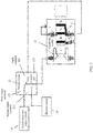
- FIG. 2 is a schematic structural diagram (which shows only parts related to an earphone socket) of a terminal that can be used in a terminal-earphone system according to an embodiment of the present invention.
- the terminal includes: an earphone socket 21, a switch circuit 22, an earphone power supply circuit 23, and a bleeder circuit 24.
- the earphone socket 21 includes a first pin 1 and a second pin 2
- the switch circuit 22 includes a control pin 223, an input terminal 220, a first output terminal 221, and a second output terminal 222.
- the first pin 1 of the earphone socket 21 is connected to the control pin 223 of the switch circuit 22
- the second pin 2 of the earphone socket 21 is connected to the input terminal 220 of the switch circuit 22
- the first output terminal 221 of the switch circuit 22 is connected to the earphone power supply circuit 23, and the second output terminal 222 of the switch circuit 22 is connected to the bleeder circuit 24.
- the bleeder circuit is configured to reduce a difference between voltages passing through an audio-left channel or an audio-right channel of the earphone, the terminal determines, by detecting a voltage of the first pin, whether the earphone is plugged or unplugged, and the terminal supplies power to the earphone by using the second pin 2. It should be noted that the terminal supplies power to or charges the earphone by using the earphone power supply circuit 23.
- the earphone power supply circuit 23 may be a circuit that supplies power to a microphone of the earphone; if the earphone is a noise reduction earphone, the earphone power supply circuit 23 may be a circuit that supplies power to or charges the earphone.
- the first earphone socket design before the earphone is plugged into the earphone socket, the first pin 1 of the earphone socket 21 is not in contact with a section L, and after the earphone is plugged into the earphone socket, the first pin 1 of the earphone socket 21 is in contact with the section L.
- the second earphone socket design before the earphone is plugged into the earphone socket, the first pin 1 of the earphone socket 21 is in contact with the section L, and after the earphone is plugged into the earphone socket, the first pin 1 of the earphone socket 21 is not in contact with the section L, that is, the first pin 1 of the earphone socket 21 flicks off.
- the input terminal 220 of the switch circuit 22 is connected to the first output terminal 221 of the switch circuit 22; or when an input voltage of the control pin 223 of the switch circuit 22 is higher than a second preset voltage value (the input voltage of the control pin 223 of the switch circuit 22 is a high level), the input terminal 220 of the switch circuit 22 is connected to the second output terminal 222 of the switch circuit 22.
- the input terminal 220 of the switch circuit 22 is connected to the first output terminal 221 of the switch circuit 22; or when an input voltage of the control pin 223 of the switch circuit 22 is lower than a second preset voltage value (the input voltage of the control pin 223 of the switch circuit 22 is a low level), the input terminal 220 of the switch circuit 22 is connected to the second output terminal 222 of the switch circuit 22.
- the first preset voltage value and the second preset voltage value are preset voltage values, and values of the first preset voltage value and the second preset voltage value may be set according to an actual requirement, which is not specifically limited.
- the voltage of the first pin 1 of the earphone socket 21 changes. Generally, when the first pin 1 of the earphone socket 21 is in contact with the earphone, the voltage of the first pin 1 of the earphone socket 21 is a low level, and the input voltage input to the control pin 223 of the switch circuit 22 is also a low level; when the first pin 1 of the earphone socket 21 is not in contact with the earphone, the voltage of the first pin 1 of the earphone socket 21 is a high level, and the input voltage of the control pin 223 of the switch circuit 22 is also a high level.
- the first type of earphone socket when the earphone is being plugged into or unplugged from the earphone socket 21, if the first pin 1 of the earphone socket 21 is not connected to the section L of the earphone, the voltage of the first pin 1 is a high level, and the input terminal 220 of the switch circuit 22 is connected to the second output terminal 222 of the switch circuit 22, that is, the earphone power supply circuit 23 and the second pin 2 of the earphone socket 21 are disconnected. Therefore, a voltage on the earphone power supply circuit 23 does not form a loop on the audio-left channel or the audio-right channel of the earphone, and no noise comes from the audio-left channel or the audio-right channel of the earphone.
- the earphone power supply circuit 23 does not form a loop on the audio-left channel or the audio-right channel of the earphone, and no noise comes from the audio-left channel or the audio-right channel of the earphone.
- a switch circuit is added into the terminal, and when an input voltage of a control pin of the switch circuit is a high level or a low level (for an earphone type used with the terminal, either of a high level and a low level is selected), an input terminal of the switch circuit is connected to a second output terminal of the switch circuit, that is, a connection between an earphone power supply circuit and a second pin of an earphone socket is disconnected.
- a voltage on the earphone power supply circuit does not form a loop on an audio-left channel or an audio-right channel of the earphone, and no noise comes from the audio-left channel or the audio-right channel of the earphone, so that noise generated when the earphone is being plugged into or unplugged from the earphone socket is effectively reduced.
- the voltage of the first pin 1 of the earphone socket 21 changes. Generally, when the first pin 1 of the earphone socket 21 is in contact with the earphone, the voltage of the first pin 1 of the earphone socket 21 is a low level; when the first pin 1 of the earphone socket 21 is not in contact with the earphone, the voltage of the first pin 1 of the earphone socket 21 is a high level. However, on some occasions, the voltage of the first pin 1 does not change obviously; therefore, the switch circuit cannot accurately determine whether the first pin 1 of the earphone socket 21 is in contact with the earphone, which may cause incorrect use of the switch circuit 22.
- the following solution manners may be used for the foregoing problem.
- the terminal further includes a CPU (not shown in the figure), where that the first pin of the earphone socket is connected to the control pin of the switch circuit is specifically: the CPU is electrically connected to the first pin 1 of the earphone socket 21, and electrically connected to the control pin of the switch circuit 22.
- the CPU is configured to: adjust the input voltage of the control pin of the switch circuit to be lower than the first preset voltage value according to the voltage of the first pin 1 of the earphone socket 21; or adjust the input voltage of the control pin of the switch circuit to be higher than the second preset voltage value according to the voltage of the first pin 1 of the earphone socket 21.
- the CPU By electrically connecting the first pin 1 of the earphone socket 21 and the control pin 223 of the switch circuit 22 to the CPU separately, the CPU adjusts the input voltage of the control pin 223 of the switch circuit 22 to be lower than the first preset voltage value according to the voltage of the first pin 1 of the earphone socket 21; or adjusts the input voltage of the control pin 223 of the switch circuit 22 to be higher than the second preset voltage value according to the voltage of the first pin 1 of the earphone socket 21. That is, the CPU adjusts a voltage obtained from the first pin 1 of the earphone socket 21 to a voltage of a high level or a low level that can be accurately identified by the control pin 223 of the switch circuit 22.
- first preset voltage value and the second preset voltage value For a specific extent of adjustment, reference may be made to the first preset voltage value and the second preset voltage value. Therefore, there is no need to add hardware, and by controlling connection and disconnection between the earphone power supply circuit 23 and the second pin 2 of the earphone socket 21 in a software manner without increasing manufacturing costs of the terminal, noise generated when the earphone is being plugged into or unplugged from the earphone socket 21 can still be effectively reduced.
- the terminal further includes a voltage adjustment unit (not shown in the figure), where that the first pin 1 of the earphone socket 21 is connected to the control pin 23 of the switch circuit 22 is specifically: the first pin 1 of the earphone socket 21 is connected to one terminal of the voltage adjustment unit, and another terminal of the voltage adjustment unit is connected to the control pin 223 of the switch circuit 22.
- the voltage adjustment unit is configured to: adjust the input voltage of the control pin 223 of the switch circuit 22 to be lower than the first preset voltage value according to the voltage of the first pin 1 of the earphone socket 21; or adjust the input voltage of the control pin 223 of the switch circuit 22 to be higher than the second preset voltage value according to the voltage of the first pin 1 of the earphone socket 211.
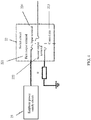
- FIG. 3 is a schematic structural diagram (which shows only parts related to an earphone socket 21) of a terminal. This terminal may be implemented based on the terminal shown in FIG. 2 . Only a part different from FIG. 2 is described herein, and for a same part, reference may be made to a description of FIG. 2 .
- the voltage adjustment unit is specifically a voltage comparator 31, where that the first pin 1 of the earphone socket 21 is connected to the control pin 223 of the switch circuit 22 is specifically (as shown in FIG. 3 ): the first pin 1 of the earphone socket 21 is connected to a first terminal of the voltage comparator 31, a second terminal of the voltage comparator 31 is connected to a reference voltage V, and a third terminal of the voltage comparator 31 is connected to the control pin 223 of the switch circuit 22.
- the voltage comparator 31 is configured to: adjust the input voltage of the control pin 223 of the switch circuit 22 to be lower than the first preset voltage value according to the voltage of the first pin 1 of the earphone socket 21 and the reference voltage V; or adjust the input voltage of the control pin 223 of the switch circuit 22 to be higher than the second preset voltage value according to the voltage of the first pin 1 of the earphone socket 21 and the reference voltage V.
- the voltage comparator 31 compares a voltage obtained from the first pin 1 of the earphone socket 21 with the reference voltage V, and adjusts a voltage that is to be output by the voltage comparator 31 to a voltage of a high level or a low level that can be accurately identified by the control pin 223 of the switch circuit 22. For a specific extent of adjustment, reference may be made to the first preset voltage value and the second preset voltage value.
- the control pin 223 of the switch circuit 22 can quickly and accurately identify a high level or a low level, so as to more accurately control connection and disconnection between the earphone power supply circuit 23 and the second pin 2 of the earphone socket 21, that is, can more accurately control a status of the switch circuit 22, thereby effectively reducing noise generated when the earphone is being plugged into or unplugged from the earphone socket 21.
- the voltage comparator is relatively common in the prior art, and a working principle of the voltage comparator is not described in detail herein.
- bleeder circuit there may be multiple specific structures for the bleeder circuit.
- the following uses an example to describe a specific structure of the bleeder circuit. Which structure is used in an actual manufacturing process of the terminal may be set according to an actual requirement, which is not specifically limited.
- the bleeder circuit 24 includes a pull-down resistor R, where one terminal of the pull-down resistor R is connected to the second output terminal 222 of the switch circuit 22, and the other terminal of the pull-down resistor R is connected to a ground of the terminal.
- the bleeder circuit 24 includes a pull-down resistor R, where one terminal of the pull-down resistor R is connected to the second output terminal 222 of the switch circuit 22, and the other terminal of the pull-down resistor R is connected to the earphone power supply circuit 23.
- the bleeder circuit is configured to reduce the difference between the voltages passing through the audio-left channel or the audio-right channel of the earphone.
- a resistance of the pull-down resistor R is less than or equal to 1 kilohm; or when the other terminal of the pull-down resistor R is connected to the earphone power supply circuit, a resistance of the pull-down resistor R is greater than or equal to 5 kilohms. In this case, the difference between the voltages passing through the audio-left channel or the audio-right channel of the earphone approximates to zero.
- a switch circuit is added into the terminal, and when an input voltage of a control pin 223 of the switch circuit is a high level or a low level (for an earphone type used with the terminal, either of a high level and a low level is selected), an input terminal 220 of the switch circuit is connected to a second output terminal 222 of the switch circuit, that is, a connection between an earphone power supply circuit 23 and a second pin 2 of an earphone socket 21 is disconnected.
- a voltage on the earphone power supply circuit does not form a loop on an audio-left channel or an audio-right channel of the earphone, and no noise comes from the audio-left channel or the audio-right channel of the earphone, so that noise generated when the earphone is being plugged into or unplugged from the earphone socket 21 is effectively reduced.
- This example makes an improvement of a terminal on the basis of the previous example, to further reduce noise generated in a process of plugging or unplugging an earphone.
- a voltage on the earphone power supply circuit 23 forms a loop on an audio-right channel of the earphone, and then noise comes from the audio-right channel of the earphone.
- a length of the second pin 2 of the earphone socket needs to be redesigned.
- a contact of the second pin 2 of the earphone socket 21 may be moved X mm in an unplugging direction of the earphone, so that the contact of the second pin 2 of the earphone socket 21 is not in contact with the section G of the earphone at a moment when the first pin 1 of the earphone socket 21 comes into contact with the section L of the earphone.
- the voltage on the earphone power supply circuit 23 does not form a loop on the audio-right channel of the earphone, and no noise comes from the audio-right channel of the earphone. Therefore, the noise generated in the process of plugging or unplugging the earphone can be eliminated.
- the following conditions need to be satisfied: After the earphone is entirely plugged into the earphone socket, the contact of the second pin of the earphone socket comes into reliable contact with the earphone; and when the earphone is being plugged into the earphone socket, the contact of the second pin of the earphone socket is not in contact with a conductive section of the earphone at a moment when the first pin of the earphone socket comes into contact with the earphone. In this case, when the first pin 1 of the earphone socket 21 is connected to the section L of the earphone, and the earphone power supply circuit 23 is connected to the second pin 2, the second pin 2 of the earphone socket 21 is not connected to the section G of the earphone.
- the voltage on the earphone power supply circuit 23 does not form a loop on the audio-right channel of the earphone, and no noise comes from the audio-right channel of the earphone. Therefore, the noise generated in the process of plugging or unplugging the earphone can be eliminated.
- the following conditions need to be satisfied: (1) After the earphone is entirely plugged into the earphone socket 21, the contact of the second pin 2 of the earphone socket 21 can come into reliable contact with a section M of the earphone; and (2) when the earphone is being plugged into the earphone socket 21, the contact of the second pin 2 of the earphone socket 21 is not in contact with the section G of the earphone at a moment when the first pin 1 of the earphone socket 21 comes into contact with the section L of the earphone.
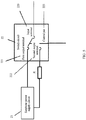
- FIG. 6 is a structural diagram of a system according to an embodiment of the present invention. As shown in FIG. 6 , the system includes the terminal and the earphone in the foregoing Embodiment 1.
- noise generated when the earphone is being plugged into or unplugged from the earphone socket noise generated in a process of plugging or unplugging the earphone is also eliminated by reducing a section (a corresponding section of a standard earphone) on an earphone side by X mm.
- the following conditions need to be satisfied: After the earphone is entirely plugged into the earphone socket, a contact of a second pin of the earphone socket comes into reliable contact with the earphone; and when the earphone is being plugged into the earphone socket, the contact of the second pin of the earphone socket is not in contact with a conductive section of the earphone at a moment when a first pin of the earphone socket comes into contact with the earphone.
- the following conditions need to be satisfied: (1) After the earphone is entirely plugged into the earphone socket 21, the contact of the second pin 2 of the earphone socket 21 comes into reliable contact with a section M of the earphone; and (2) when the earphone is being plugged into the earphone socket 21, the contact of the second pin 2 of the earphone socket 21 is not in contact with a section G of the earphone at a moment when a first pin 1 of the earphone socket 21 comes into contact with a section L of the earphone.
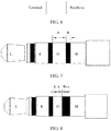
- FIG. 7 is a schematic structural diagram of a standard earphone in the prior art.
- a line order of the standard earphone is L, R, G, and M from left to right
- a length of the section G of the standard earphone is A mm
- a length of an insulation layer between the section G and the section M is B mm.
- FIG. 8 is a schematic structural diagram of an improved earphone according to an embodiment of the present invention.
- FIG. 8 shows a modification to the standard earphone on the basis of FIG. 7 , that is, a length of the section G of the improved earphone is reduced by X mm compared with that of the section G of the standard earphone.
- the length of the insulation layer between the section G and the section M is (B+X) mm.
- a switch circuit is added into a terminal, and a length of a section of an earphone is shortened, so that a voltage on an earphone power supply circuit 23 does not form a loop on an audio-left channel or an audio-right channel of the earphone, and no noise comes from the audio-left channel or the audio-right channel of the earphone. Therefore, noise generated when the earphone is being plugged into or unplugged from an earphone socket 21 is eliminated.
Landscapes
- Physics & Mathematics (AREA)
- Engineering & Computer Science (AREA)
- Acoustics & Sound (AREA)
- Signal Processing (AREA)
- Health & Medical Sciences (AREA)
- General Health & Medical Sciences (AREA)
- Otolaryngology (AREA)
- Headphones And Earphones (AREA)
Applications Claiming Priority (2)
| Application Number | Priority Date | Filing Date | Title |
|---|---|---|---|
| CN2014081229 | 2014-06-30 | ||
| PCT/CN2014/081661 WO2016000261A1 (zh) | 2014-06-30 | 2014-07-04 | 一种可减少耳机插拔过程中噪音的终端及系统 |
Publications (3)
| Publication Number | Publication Date |
|---|---|
| EP3131310A1 EP3131310A1 (en) | 2017-02-15 |
| EP3131310A4 EP3131310A4 (en) | 2017-04-12 |
| EP3131310B1 true EP3131310B1 (en) | 2019-07-03 |
Family
ID=55018338
Family Applications (1)
| Application Number | Title | Priority Date | Filing Date |
|---|---|---|---|
| EP14896799.5A Active EP3131310B1 (en) | 2014-06-30 | 2014-07-04 | System of terminal and earphone capable of reducing noises generated in earphone insertion and pulling processes |
Country Status (5)
| Country | Link |
|---|---|
| US (1) | US20170078797A1 (ko) |
| EP (1) | EP3131310B1 (ko) |
| JP (1) | JP6423457B2 (ko) |
| KR (1) | KR20160148668A (ko) |
| WO (1) | WO2016000261A1 (ko) |
Citations (1)
| Publication number | Priority date | Publication date | Assignee | Title |
|---|---|---|---|---|
| US20130078869A1 (en) * | 2010-05-28 | 2013-03-28 | Apple Inc. | D-shaped connector |
Family Cites Families (10)
| Publication number | Priority date | Publication date | Assignee | Title |
|---|---|---|---|---|
| US8861743B2 (en) * | 2008-05-30 | 2014-10-14 | Apple Inc. | Headset microphone type detect |
| CN101630802B (zh) * | 2008-07-15 | 2013-06-05 | 深圳富泰宏精密工业有限公司 | 耳机插孔结构 |
| EP3001698B1 (en) * | 2009-02-26 | 2019-07-03 | BlackBerry Limited | Portable electronic device with an audio jack |
| CN101841588B (zh) * | 2009-03-17 | 2014-04-30 | 深圳富泰宏精密工业有限公司 | 音频接口装置及使用该音频接口装置的电子装置 |
| KR101267047B1 (ko) * | 2012-03-30 | 2013-05-24 | 삼성전자주식회사 | 이어폰 인식 장치 및 방법 |
| US9210500B2 (en) * | 2012-08-17 | 2015-12-08 | Cirrus Logic, Inc. | Headset type detection and configuration techniques |
| KR101937839B1 (ko) * | 2012-08-29 | 2019-04-10 | 삼성전자 주식회사 | 이어폰 접속 인터페이스 및 이를 포함하는 단말기와 단말기 운용 방법 |
| CN103022831A (zh) * | 2012-12-30 | 2013-04-03 | 青岛歌尔声学科技有限公司 | 耳机插座、耳机降噪装置和耳机插座的实现方法 |
| CN103024632B (zh) * | 2012-12-30 | 2016-06-01 | 青岛歌尔声学科技有限公司 | 一种耳机降噪装置 |
| CN103414984A (zh) * | 2013-07-25 | 2013-11-27 | 苏州三星电子电脑有限公司 | 耳机爆破音消除系统 |
-
2014
- 2014-07-04 WO PCT/CN2014/081661 patent/WO2016000261A1/zh active Application Filing
- 2014-07-04 EP EP14896799.5A patent/EP3131310B1/en active Active
- 2014-07-04 KR KR1020167033425A patent/KR20160148668A/ko not_active Application Discontinuation
- 2014-07-04 JP JP2016572328A patent/JP6423457B2/ja active Active
- 2014-07-04 US US15/311,334 patent/US20170078797A1/en not_active Abandoned
Patent Citations (1)
| Publication number | Priority date | Publication date | Assignee | Title |
|---|---|---|---|---|
| US20130078869A1 (en) * | 2010-05-28 | 2013-03-28 | Apple Inc. | D-shaped connector |
Non-Patent Citations (1)
| Title |
|---|
| "Technical requirements and test methods for universal wired headset or headphone interface of digital wireless terminals; P.381 (02/14)", no. P.381 (02/14), 13 February 2014 (2014-02-13), pages 1 - 58, XP044180157, Retrieved from the Internet <URL:http://mirror.itu.int/dms/pay/itu-t/rec/p/T-REC-P.381-201402-S!!PDF-E.pdf> [retrieved on 20150123] * |
Also Published As
| Publication number | Publication date |
|---|---|
| JP6423457B2 (ja) | 2018-11-14 |
| US20170078797A1 (en) | 2017-03-16 |
| WO2016000261A1 (zh) | 2016-01-07 |
| EP3131310A4 (en) | 2017-04-12 |
| KR20160148668A (ko) | 2016-12-26 |
| EP3131310A1 (en) | 2017-02-15 |
| JP2017523663A (ja) | 2017-08-17 |
Similar Documents
| Publication | Publication Date | Title |
|---|---|---|
| EP3416062B1 (en) | Method and terminal device for establishing connection between devices with universal serial bus usb type-c interface | |
| US8467540B2 (en) | Electronic device and method thereof for switching audio input channel of the electronic device | |
| US7635265B2 (en) | Electrical volume control using contacts on rotatable connector, and method | |
| CN105933823B (zh) | 使用4p音频插头向具有有源噪声抵消的耳机提供功率和信号的向后兼容的系统以及方法 | |
| DK2950552T3 (en) | Headphone and method for automatic selection of remote control circuits for a headphone | |
| EP2637421A2 (en) | Earphone jack drive circuit | |
| CN101271433B (zh) | 自动的计算机音频输入及输出控制 | |
| KR20130056404A (ko) | 휴대 단말기의 이어폰 인식 방법 및 장치 | |
| US11316308B2 (en) | Adapter, multi-device detection system and detection method thereof | |
| KR20190037834A (ko) | 외부 마이크로폰의 그라운드 단자와 전기적으로 연결될 수 있는 커넥터에 포함된 지정된 핀이 회로 기판의 지정된 그라운드와 전기적으로 연결된 회로 구조를 갖는 전자 장치 | |
| KR20140126491A (ko) | 전자 장치의 전원 공급 회로 및 그 제어 방법 | |
| EP3131310B1 (en) | System of terminal and earphone capable of reducing noises generated in earphone insertion and pulling processes | |
| EP3940525A1 (en) | Audio circuit, related device and control method | |
| US20150325960A1 (en) | Universal serial bus interface and mobile device | |
| CN104380697B (zh) | 一种可减少耳机插拔过程中噪音的终端及系统 | |
| US20130300214A1 (en) | Transmission cable, electronic device using the same, and method for switching operation mode of the electronic device | |
| US10051395B2 (en) | Accessory management and data communication using audio port | |
| CN105512067A (zh) | 一种移动终端及其端口复用电路和方法 | |
| EP2690884A2 (en) | Audio device with mute function | |
| CN105812980A (zh) | 耳机 | |
| EP3214855B1 (en) | Device and method for adjusting an output to an audio port based on a determined sensitivity | |
| US9667526B2 (en) | Mobile terminal | |
| CN108111951B (zh) | 一种可减少耳机插拔过程中噪音的终端及系统 | |
| EP3345405B1 (en) | Microphone compatibility | |
| CN114554084B (zh) | 一种基于stm32单片机的多设备协同拍照系统 |
Legal Events
| Date | Code | Title | Description |
|---|---|---|---|
| STAA | Information on the status of an ep patent application or granted ep patent |
Free format text: STATUS: THE INTERNATIONAL PUBLICATION HAS BEEN MADE |
|
| PUAI | Public reference made under article 153(3) epc to a published international application that has entered the european phase |
Free format text: ORIGINAL CODE: 0009012 |
|
| STAA | Information on the status of an ep patent application or granted ep patent |
Free format text: STATUS: REQUEST FOR EXAMINATION WAS MADE |
|
| 17P | Request for examination filed |
Effective date: 20161111 |
|
| AK | Designated contracting states |
Kind code of ref document: A1 Designated state(s): AL AT BE BG CH CY CZ DE DK EE ES FI FR GB GR HR HU IE IS IT LI LT LU LV MC MK MT NL NO PL PT RO RS SE SI SK SM TR |
|
| AX | Request for extension of the european patent |
Extension state: BA ME |
|
| A4 | Supplementary search report drawn up and despatched |
Effective date: 20170310 |
|
| RIC1 | Information provided on ipc code assigned before grant |
Ipc: H04R 29/00 20060101ALI20170306BHEP Ipc: H04R 3/00 20060101AFI20170306BHEP |
|
| DAX | Request for extension of the european patent (deleted) | ||
| STAA | Information on the status of an ep patent application or granted ep patent |
Free format text: STATUS: EXAMINATION IS IN PROGRESS |
|
| 17Q | First examination report despatched |
Effective date: 20180112 |
|
| RIC1 | Information provided on ipc code assigned before grant |
Ipc: H04R 3/00 20060101AFI20181212BHEP Ipc: H04R 29/00 20060101ALI20181212BHEP Ipc: H04R 1/10 20060101ALI20181212BHEP Ipc: H01R 24/58 20110101ALI20181212BHEP Ipc: H01R 107/00 20060101ALN20181212BHEP |
|
| GRAP | Despatch of communication of intention to grant a patent |
Free format text: ORIGINAL CODE: EPIDOSNIGR1 |
|
| STAA | Information on the status of an ep patent application or granted ep patent |
Free format text: STATUS: GRANT OF PATENT IS INTENDED |
|
| RIC1 | Information provided on ipc code assigned before grant |
Ipc: H04R 1/10 20060101ALI20181219BHEP Ipc: H04R 29/00 20060101ALI20181219BHEP Ipc: H01R 107/00 20060101ALN20181219BHEP Ipc: H01R 24/58 20110101ALI20181219BHEP Ipc: H04R 3/00 20060101AFI20181219BHEP |
|
| INTG | Intention to grant announced |
Effective date: 20190122 |
|
| GRAS | Grant fee paid |
Free format text: ORIGINAL CODE: EPIDOSNIGR3 |
|
| GRAA | (expected) grant |
Free format text: ORIGINAL CODE: 0009210 |
|
| STAA | Information on the status of an ep patent application or granted ep patent |
Free format text: STATUS: THE PATENT HAS BEEN GRANTED |
|
| AK | Designated contracting states |
Kind code of ref document: B1 Designated state(s): AL AT BE BG CH CY CZ DE DK EE ES FI FR GB GR HR HU IE IS IT LI LT LU LV MC MK MT NL NO PL PT RO RS SE SI SK SM TR |
|
| REG | Reference to a national code |
Ref country code: GB Ref legal event code: FG4D |
|
| REG | Reference to a national code |
Ref country code: CH Ref legal event code: EP Ref country code: AT Ref legal event code: REF Ref document number: 1152436 Country of ref document: AT Kind code of ref document: T Effective date: 20190715 |
|
| REG | Reference to a national code |
Ref country code: IE Ref legal event code: FG4D |
|
| REG | Reference to a national code |
Ref country code: DE Ref legal event code: R096 Ref document number: 602014049697 Country of ref document: DE |
|
| REG | Reference to a national code |
Ref country code: NL Ref legal event code: FP |
|
| REG | Reference to a national code |
Ref country code: LT Ref legal event code: MG4D |
|
| REG | Reference to a national code |
Ref country code: AT Ref legal event code: MK05 Ref document number: 1152436 Country of ref document: AT Kind code of ref document: T Effective date: 20190703 |
|
| PG25 | Lapsed in a contracting state [announced via postgrant information from national office to epo] |
Ref country code: FI Free format text: LAPSE BECAUSE OF FAILURE TO SUBMIT A TRANSLATION OF THE DESCRIPTION OR TO PAY THE FEE WITHIN THE PRESCRIBED TIME-LIMIT Effective date: 20190703 Ref country code: LT Free format text: LAPSE BECAUSE OF FAILURE TO SUBMIT A TRANSLATION OF THE DESCRIPTION OR TO PAY THE FEE WITHIN THE PRESCRIBED TIME-LIMIT Effective date: 20190703 Ref country code: HR Free format text: LAPSE BECAUSE OF FAILURE TO SUBMIT A TRANSLATION OF THE DESCRIPTION OR TO PAY THE FEE WITHIN THE PRESCRIBED TIME-LIMIT Effective date: 20190703 Ref country code: SE Free format text: LAPSE BECAUSE OF FAILURE TO SUBMIT A TRANSLATION OF THE DESCRIPTION OR TO PAY THE FEE WITHIN THE PRESCRIBED TIME-LIMIT Effective date: 20190703 Ref country code: NO Free format text: LAPSE BECAUSE OF FAILURE TO SUBMIT A TRANSLATION OF THE DESCRIPTION OR TO PAY THE FEE WITHIN THE PRESCRIBED TIME-LIMIT Effective date: 20191003 Ref country code: AT Free format text: LAPSE BECAUSE OF FAILURE TO SUBMIT A TRANSLATION OF THE DESCRIPTION OR TO PAY THE FEE WITHIN THE PRESCRIBED TIME-LIMIT Effective date: 20190703 Ref country code: PT Free format text: LAPSE BECAUSE OF FAILURE TO SUBMIT A TRANSLATION OF THE DESCRIPTION OR TO PAY THE FEE WITHIN THE PRESCRIBED TIME-LIMIT Effective date: 20191104 Ref country code: CZ Free format text: LAPSE BECAUSE OF FAILURE TO SUBMIT A TRANSLATION OF THE DESCRIPTION OR TO PAY THE FEE WITHIN THE PRESCRIBED TIME-LIMIT Effective date: 20190703 Ref country code: BG Free format text: LAPSE BECAUSE OF FAILURE TO SUBMIT A TRANSLATION OF THE DESCRIPTION OR TO PAY THE FEE WITHIN THE PRESCRIBED TIME-LIMIT Effective date: 20191003 |
|
| PG25 | Lapsed in a contracting state [announced via postgrant information from national office to epo] |
Ref country code: ES Free format text: LAPSE BECAUSE OF FAILURE TO SUBMIT A TRANSLATION OF THE DESCRIPTION OR TO PAY THE FEE WITHIN THE PRESCRIBED TIME-LIMIT Effective date: 20190703 Ref country code: LV Free format text: LAPSE BECAUSE OF FAILURE TO SUBMIT A TRANSLATION OF THE DESCRIPTION OR TO PAY THE FEE WITHIN THE PRESCRIBED TIME-LIMIT Effective date: 20190703 Ref country code: AL Free format text: LAPSE BECAUSE OF FAILURE TO SUBMIT A TRANSLATION OF THE DESCRIPTION OR TO PAY THE FEE WITHIN THE PRESCRIBED TIME-LIMIT Effective date: 20190703 Ref country code: IS Free format text: LAPSE BECAUSE OF FAILURE TO SUBMIT A TRANSLATION OF THE DESCRIPTION OR TO PAY THE FEE WITHIN THE PRESCRIBED TIME-LIMIT Effective date: 20191103 Ref country code: RS Free format text: LAPSE BECAUSE OF FAILURE TO SUBMIT A TRANSLATION OF THE DESCRIPTION OR TO PAY THE FEE WITHIN THE PRESCRIBED TIME-LIMIT Effective date: 20190703 Ref country code: GR Free format text: LAPSE BECAUSE OF FAILURE TO SUBMIT A TRANSLATION OF THE DESCRIPTION OR TO PAY THE FEE WITHIN THE PRESCRIBED TIME-LIMIT Effective date: 20191004 |
|
| REG | Reference to a national code |
Ref country code: CH Ref legal event code: PL |
|
| PG25 | Lapsed in a contracting state [announced via postgrant information from national office to epo] |
Ref country code: TR Free format text: LAPSE BECAUSE OF FAILURE TO SUBMIT A TRANSLATION OF THE DESCRIPTION OR TO PAY THE FEE WITHIN THE PRESCRIBED TIME-LIMIT Effective date: 20190703 |
|
| REG | Reference to a national code |
Ref country code: BE Ref legal event code: MM Effective date: 20190731 |
|
| PG25 | Lapsed in a contracting state [announced via postgrant information from national office to epo] |
Ref country code: EE Free format text: LAPSE BECAUSE OF FAILURE TO SUBMIT A TRANSLATION OF THE DESCRIPTION OR TO PAY THE FEE WITHIN THE PRESCRIBED TIME-LIMIT Effective date: 20190703 Ref country code: PL Free format text: LAPSE BECAUSE OF FAILURE TO SUBMIT A TRANSLATION OF THE DESCRIPTION OR TO PAY THE FEE WITHIN THE PRESCRIBED TIME-LIMIT Effective date: 20190703 Ref country code: RO Free format text: LAPSE BECAUSE OF FAILURE TO SUBMIT A TRANSLATION OF THE DESCRIPTION OR TO PAY THE FEE WITHIN THE PRESCRIBED TIME-LIMIT Effective date: 20190703 Ref country code: IT Free format text: LAPSE BECAUSE OF FAILURE TO SUBMIT A TRANSLATION OF THE DESCRIPTION OR TO PAY THE FEE WITHIN THE PRESCRIBED TIME-LIMIT Effective date: 20190703 Ref country code: DK Free format text: LAPSE BECAUSE OF FAILURE TO SUBMIT A TRANSLATION OF THE DESCRIPTION OR TO PAY THE FEE WITHIN THE PRESCRIBED TIME-LIMIT Effective date: 20190703 |
|
| PG25 | Lapsed in a contracting state [announced via postgrant information from national office to epo] |
Ref country code: LU Free format text: LAPSE BECAUSE OF NON-PAYMENT OF DUE FEES Effective date: 20190704 Ref country code: IS Free format text: LAPSE BECAUSE OF FAILURE TO SUBMIT A TRANSLATION OF THE DESCRIPTION OR TO PAY THE FEE WITHIN THE PRESCRIBED TIME-LIMIT Effective date: 20200224 Ref country code: SK Free format text: LAPSE BECAUSE OF FAILURE TO SUBMIT A TRANSLATION OF THE DESCRIPTION OR TO PAY THE FEE WITHIN THE PRESCRIBED TIME-LIMIT Effective date: 20190703 Ref country code: CH Free format text: LAPSE BECAUSE OF NON-PAYMENT OF DUE FEES Effective date: 20190731 Ref country code: BE Free format text: LAPSE BECAUSE OF NON-PAYMENT OF DUE FEES Effective date: 20190731 Ref country code: LI Free format text: LAPSE BECAUSE OF NON-PAYMENT OF DUE FEES Effective date: 20190731 Ref country code: SM Free format text: LAPSE BECAUSE OF FAILURE TO SUBMIT A TRANSLATION OF THE DESCRIPTION OR TO PAY THE FEE WITHIN THE PRESCRIBED TIME-LIMIT Effective date: 20190703 Ref country code: MC Free format text: LAPSE BECAUSE OF FAILURE TO SUBMIT A TRANSLATION OF THE DESCRIPTION OR TO PAY THE FEE WITHIN THE PRESCRIBED TIME-LIMIT Effective date: 20190703 |
|
| REG | Reference to a national code |
Ref country code: DE Ref legal event code: R097 Ref document number: 602014049697 Country of ref document: DE |
|
| PLBE | No opposition filed within time limit |
Free format text: ORIGINAL CODE: 0009261 |
|
| STAA | Information on the status of an ep patent application or granted ep patent |
Free format text: STATUS: NO OPPOSITION FILED WITHIN TIME LIMIT |
|
| PG2D | Information on lapse in contracting state deleted |
Ref country code: IS |
|
| PG25 | Lapsed in a contracting state [announced via postgrant information from national office to epo] |
Ref country code: IE Free format text: LAPSE BECAUSE OF NON-PAYMENT OF DUE FEES Effective date: 20190704 |
|
| 26N | No opposition filed |
Effective date: 20200603 |
|
| PG25 | Lapsed in a contracting state [announced via postgrant information from national office to epo] |
Ref country code: SI Free format text: LAPSE BECAUSE OF FAILURE TO SUBMIT A TRANSLATION OF THE DESCRIPTION OR TO PAY THE FEE WITHIN THE PRESCRIBED TIME-LIMIT Effective date: 20190703 |
|
| PG25 | Lapsed in a contracting state [announced via postgrant information from national office to epo] |
Ref country code: CY Free format text: LAPSE BECAUSE OF FAILURE TO SUBMIT A TRANSLATION OF THE DESCRIPTION OR TO PAY THE FEE WITHIN THE PRESCRIBED TIME-LIMIT Effective date: 20190703 |
|
| PG25 | Lapsed in a contracting state [announced via postgrant information from national office to epo] |
Ref country code: MT Free format text: LAPSE BECAUSE OF FAILURE TO SUBMIT A TRANSLATION OF THE DESCRIPTION OR TO PAY THE FEE WITHIN THE PRESCRIBED TIME-LIMIT Effective date: 20190703 Ref country code: HU Free format text: LAPSE BECAUSE OF FAILURE TO SUBMIT A TRANSLATION OF THE DESCRIPTION OR TO PAY THE FEE WITHIN THE PRESCRIBED TIME-LIMIT; INVALID AB INITIO Effective date: 20140704 |
|
| PG25 | Lapsed in a contracting state [announced via postgrant information from national office to epo] |
Ref country code: MK Free format text: LAPSE BECAUSE OF FAILURE TO SUBMIT A TRANSLATION OF THE DESCRIPTION OR TO PAY THE FEE WITHIN THE PRESCRIBED TIME-LIMIT Effective date: 20190703 |
|
| PGFP | Annual fee paid to national office [announced via postgrant information from national office to epo] |
Ref country code: NL Payment date: 20230614 Year of fee payment: 10 Ref country code: FR Payment date: 20230620 Year of fee payment: 10 |
|
| PGFP | Annual fee paid to national office [announced via postgrant information from national office to epo] |
Ref country code: GB Payment date: 20230601 Year of fee payment: 10 |
|
| PGFP | Annual fee paid to national office [announced via postgrant information from national office to epo] |
Ref country code: DE Payment date: 20230531 Year of fee payment: 10 |