EP3131169A1 - Frequency control device for dc interconnection system and dc interconnection system - Google Patents
Frequency control device for dc interconnection system and dc interconnection system Download PDFInfo
- Publication number
- EP3131169A1 EP3131169A1 EP15776473.9A EP15776473A EP3131169A1 EP 3131169 A1 EP3131169 A1 EP 3131169A1 EP 15776473 A EP15776473 A EP 15776473A EP 3131169 A1 EP3131169 A1 EP 3131169A1
- Authority
- EP
- European Patent Office
- Prior art keywords
- direct current
- frequency
- frequency deviation
- power
- current interconnection
- Prior art date
- Legal status (The legal status is an assumption and is not a legal conclusion. Google has not performed a legal analysis and makes no representation as to the accuracy of the status listed.)
- Granted
Links
Images



Classifications
-
- H—ELECTRICITY
- H02—GENERATION; CONVERSION OR DISTRIBUTION OF ELECTRIC POWER
- H02J—ELECTRIC POWER NETWORKS; CIRCUIT ARRANGEMENTS OR SYSTEMS FOR SUPPLYING OR DISTRIBUTING ELECTRIC POWER; SYSTEMS FOR STORING ELECTRIC ENERGY
- H02J3/00—Circuit arrangements for AC mains or AC distribution networks
- H02J3/36—Arrangements for transfer of electric power between AC networks via high-voltage DC [HVDC] links; Arrangements for transfer of electric power between generators and networks via HVDC links
-
- H—ELECTRICITY
- H02—GENERATION; CONVERSION OR DISTRIBUTION OF ELECTRIC POWER
- H02J—ELECTRIC POWER NETWORKS; CIRCUIT ARRANGEMENTS OR SYSTEMS FOR SUPPLYING OR DISTRIBUTING ELECTRIC POWER; SYSTEMS FOR STORING ELECTRIC ENERGY
- H02J3/00—Circuit arrangements for AC mains or AC distribution networks
- H02J3/04—Arrangements for connecting networks of the same frequency but supplied from different sources
- H02J3/06—Controlling the transfer of power between connected networks; Controlling load sharing between connected networks
-
- Y—GENERAL TAGGING OF NEW TECHNOLOGICAL DEVELOPMENTS; GENERAL TAGGING OF CROSS-SECTIONAL TECHNOLOGIES SPANNING OVER SEVERAL SECTIONS OF THE IPC; TECHNICAL SUBJECTS COVERED BY FORMER USPC CROSS-REFERENCE ART COLLECTIONS [XRACs] AND DIGESTS
- Y02—TECHNOLOGIES OR APPLICATIONS FOR MITIGATION OR ADAPTATION AGAINST CLIMATE CHANGE
- Y02E—REDUCTION OF GREENHOUSE GAS [GHG] EMISSIONS, RELATED TO ENERGY GENERATION, TRANSMISSION OR DISTRIBUTION
- Y02E60/00—Enabling technologies; Technologies with a potential or indirect contribution to GHG emissions mitigation
- Y02E60/60—Arrangements for transfer of electric power between AC networks or generators via a high voltage DC link [HVCD]
Definitions
- the present invention relates to a frequency control apparatus for a direct current interconnection system, and to a direct current interconnection system.
- the technology pays special attention to the fundamental waves generated by electric instruments and harmonic currents and the phases corresponding to the voltages, and applies a neural network. Based on the measurement data on voltages and currents measured in the neighborhood of the lead-in port of the feeding line, the technology individually estimates the operating condition of each electric instrument.
- An apparatus for reliably checking the ON/OFF operation of an electric instrument and estimating the type of electric instrument in the loaded condition is also known in the art.
- the apparatus detects which electric instrument is in the loaded condition from among a plurality of electric instruments located downstream of a measurement point and connected through a switch means and estimates the type of electric instrument in the loaded condition, based on the electricity quantity detection results at the measuring point.
- An instrument condition detector is also known in the art, which accurately detects the operating conditions of electric instruments with no need to learn the combinations of operating conditions of electric instruments to be detected.
- the instrument condition detector calculates the feature amount of each frequency component based on the measurements of currents and voltages. To identify an electric instrument, the instrument condition detector searches a database in which identification information for identifying electric instruments, feature amounts and operating conditions are associated with one another. The instrument condition detector compares calculated feature amounts with the feature amounts stored in the database, determines whether the calculated feature amounts are identical to those stored in the database, and identifies the electric instruments based on the determination.
- a change (correction value) of the required interchange power is determined in accordance with the frequency deviation.
- the change of the required interchange power has to be equal to the total sum of the interchange powers of the direct current interconnection systems.
- the changes of interchange power calculated by the direct current interconnection systems are adjusted to be small values in accordance with the number of direct current interconnection systems, the total value of the changes of interchange power may be small, if some of the direct current interconnection systems stop. As a result, the frequency control effect is affected, accordingly.
- a frequency control apparatus is a frequency control apparatus for a plurality of direct current interconnection systems which interconnect two power systems and control frequencies.
- the frequency control apparatus includes: a frequency deviation detector for detecting frequency deviations of the two power systems, a specific frequency deviation extractor for extracting a specific frequency deviation satisfying a predetermined condition from the frequency deviations detected by the frequency deviation detector; and a control switching unit for switching from frequency control which interchanges power between the two power systems in such a manner as to minimize the specific frequency deviation extracted by the specific frequency deviation extractor to frequency control which interchanges power between the two power systems in such a manner as to minimize the frequency deviation detected by the frequency deviation detector.
- FIG. 1 illustrates a configuration example of direct current interconnection systems 1a, 1b and 1c according to the first embodiment.
- like reference numerals denote like parts, and a detailed description to such parts will be omitted. A description will be given mainly of different parts.
- Two power systems 2 ⁇ and 2 ⁇ are interconnected by three direct current interconnection systems 1a, 1b and 1c.
- Direct current interconnection system 1a comprises a direct current interconnection main circuit 3a and a frequency control apparatus 10a.
- the frequency control apparatus 10a includes two frequency detectors 4 ⁇ a and 4 ⁇ a, and further includes a subtractor (frequency deviation detector) 5a, a dead band filter (specific frequency deviation extractor) 6a, a frequency controller 7a, a converter controller 8a and a mode switching unit (control switching unit) 9a.
- Direct current interconnection system 1b comprises a direct current interconnection main circuit 3b and a frequency control apparatus 10b.
- the frequency control apparatus 10b includes two frequency detectors 4 ⁇ b and 4 ⁇ b, and further includes a subtractor 5b, a dead band filter 6b, a frequency controller 7b, a converter controller 8b and a mode switching unit 9b.
- Direct current interconnection system 1c comprises a direct current interconnection main circuit 3c and a frequency control apparatus 10c.
- the frequency control apparatus 10c includes two frequency detectors 4 ⁇ c and 4 ⁇ c, and further includes a subtractor 5c, a dead band filter 6c, a frequency controller 7c, a converter controller 8c and a mode switching unit 9c.
- direct current interconnection system 1a Since the three direct current interconnection systems 1a-1c are similar in configurations, direct current interconnection system 1a will be mainly described below. With respect to the other two direct current interconnection systems 1b and 1c, a description will be given mainly of how they are different from direct current interconnection system 1a.
- FIG. 2 illustrates a configuration example of the direct current interconnection main circuit 3a and converter controller 8a of the first embodiment.
- the direct current interconnection main circuit 3a includes two converters 31 ⁇ a and 31 ⁇ a, two transformer 32 ⁇ a and 32 ⁇ a for converters, a direct current reactor 33a, a direct current detector 34, and a DC voltage detector 35.
- the two converters 31 ⁇ a and 31 ⁇ a are a pair of converters, one (31 ⁇ a) of which performs ac-to-dc voltage conversion and the other (31 ⁇ a) performs dc-to-ac voltage conversion.
- the two converters 31 ⁇ a and 31 ⁇ a are connected to each other as a DC circuit, with the direct current reactor 33a interposed therebetween.
- Converter 31 ⁇ a for dc-to-ac voltage conversion is connected to power system 2 ⁇ by way of conversion transformer 32 ⁇ a.
- Converter 31 ⁇ a for dc-to-ac voltage conversion is connected to power system 2 ⁇ by way of conversion transformer 32 ⁇ a.
- the direct current detector 34 and the DC voltage detector 35 are provided in the DC circuit.
- the direct current detector 34 detects direct current Idc flowing through the DC circuit and outputs a detection result to the converter controller 8a.
- the DC voltage detector 35 detects direct current Edc flowing through the DC circuit and outputs a detection result to the converter controller 8a.
- the converter controller 8a comprises an adder 81a, a current command value operation unit 82a, subtractor 83a, a direct current controller 84a, subtractor 85a, and a DC voltage controller 86a.
- the adder 81a receives interchange power command value Pref and also receives interchange power correction value ⁇ Pa calculated by frequency controller 7a and handled by direct current interconnection system 1a.
- the interchange power command value Pref is provided by an upper-level system such as a feeding power direction center.
- the adder 81a adds the interchange power correction value ⁇ Pa to the interchange power command value Pref, and supplies interchange power command value Pref1 obtained thereby by this addition to the current command value operation unit 82a.
- the current command value operation unit 82a calculates a direct current command value Idcref so that the interchange power can satisfy the interchange power command value Pref1, and supplies the calculated direct current command value Idcref to subtractor 83a.
- Subtractor 83a receives the direct current command value Idcref calculated by the current command value operation unit 82a and a direct current Idc detected by the direct current detector 34. Subtractor 83a subtracts the direct current command value Idcref from the direct current Idc, and supplies the resultant difference to the direct current controller 84a.
- the direct current controller 84a supplies a control command S ⁇ a to the converter 31 ⁇ a of the direct current interconnection main circuit 3a.
- the control command S ⁇ a is used for controlling the output of the converter 31 ⁇ a so that the direct current Idc can become equal to the direct current command value Idcref.
- the converter 31 ⁇ a performs ac-to-dc voltage conversion in accordance with the control command S ⁇ a.
- Subtractor 85a receives a rated voltage value Edcref of the DC circuit, and also receives a DC voltage Edc detected by the DC voltage detector 35. Subtractor 85a subtracts the DC voltage EDc from the rated voltage value Edcref, and supplies the resultant difference to the DC voltage controller 86a.
- the DC voltage controller 86a supplies a control command S ⁇ a to the converter 31 ⁇ a of the direct current interconnection main circuit 3a.
- the control command S ⁇ a is used for controlling the output of the converter 31 ⁇ a so that the DC voltage Edc can become equal to the rated voltage value Edcref.
- the converter 31 ⁇ a performs dc-to-ac voltage conversion in accordance with the control command S ⁇ a.
- the converter controller 8a interchanges power between the two power systems 2 ⁇ and 2 ⁇ by controlling the two converters 31 ⁇ a and 31 ⁇ a of the direct current interconnection main circuit 3a. For example, when the frequency f ⁇ a of power system 2 ⁇ increases, the sum of the interchange power command value Pref and the interchange power correction value ⁇ Pa increases. Accordingly, the power provided from power system 2 ⁇ to power system 2 ⁇ increases. Since the surplus power of power system 2 ⁇ decreases, the frequency increase is suppressed.
- Frequency detector 4 ⁇ a detects frequency f ⁇ a of the voltage of power system 2 ⁇ . Frequency detector 4 ⁇ a detects frequency f ⁇ a of the voltage of power system 2 ⁇ . Frequency detector 4 ⁇ a supplies the detected frequency f ⁇ a to subtractor 5a. Frequency detector 4 ⁇ a supplies the detected frequency f ⁇ a to subtractor 5a.
- the frequency deviation ⁇ fa supplied from subtractor 5a is made to pass through the dead band filter 6a (the dead frequency band of which is predetermined), and the resultant frequency deviation ⁇ fa is supplied to the frequency controller 7a. If the frequency deviation ⁇ fa is within the predetermined dead band, the output of the dead band filter 6a is zero. If the frequency deviation ⁇ fa is outside the predetermined dead band, the frequency deviation ⁇ fa received from subtractor 5a is output from the dead band filter 6a as it is.
- the frequency controller 7a calculates an interchange power correction value ⁇ Pa in accordance with the frequency deviation ⁇ fa supplied from the dead band filter 6a.
- the frequency controller 7a is made, for example, of a comparison circuit.
- the interchange power correction value ⁇ Pa calculated by frequency controller 7a is a correction value handled by direct current interconnection system 1a.
- the frequency controller 7a supplies the calculated interchange power correction value ⁇ Pa to the converter controller 8a. Based on this correction value, power is interchanged between the two converters 31 ⁇ a and 31 ⁇ a in such a manner that the frequency deviation ⁇ fa is minimized (becomes closer to zero).
- the mode switching unit 9a switches the operation mode of the direct current interconnection system 1a between a main mode and a sub mode.
- the main mode is an operation mode which plays a central role in the frequency control when the three direct current interconnection systems 1a to 1c are operated.
- the sub mode is an operation mode which plays a peripheral role in the frequency control when the three direct current interconnection systems are operated.
- the mode switching unit 9a performs control so that another direct current interconnection system can take over the function of the main mode.
- the mode switching unit 9a includes a fluctuation detector 91a, a level detector 92a and a switching determination unit 93a.
- the fluctuation detector 91a receives a frequency deviation ⁇ fa supplied from the subtractor 5a.
- the fluctuation detector 91a extracts a fluctuation component from the received frequency deviation ⁇ fa.
- the fluctuation detector 91a is made, for example, of an incomplete differentiator.
- the fluctuation detector 91a supplies the extracted fluctuation component of the frequency deviation ⁇ fa to the level detector 92a.
- the level detector 92a receives the fluctuation component of the frequency deviation ⁇ fa, which is extracted by the fluctuation detector 91a. If the absolute value of the fluctuation component of the frequency deviation ⁇ fa is equal to or more than a predetermined threshold, the level detector 92a supplies "1" to the switching determination unit 93a. If that absolute value is less than the predetermined threshold, the level detector 92a supplies "0" to the switching determination unit 93a.
- Reference time Tsh is a time used for determining whether or not the fluctuation in the frequency deviation ⁇ fa is frequent.
- Reference time Tsh is, for example, one minute.
- Reference time Tch is a time used for determining whether the fluctuation in the frequency deviation ⁇ fa continues for a long time.
- Reference time Tch is, for example, 10 minutes or 20 minutes.
- Reference time Tch differs, depending upon the direct current interconnection systems 1a to 1c.
- Short reference time Tch is determined for a direct current interconnection system which is switched to the main mode in preference to others.
- a value output from the level detector 92a is received by the switching determination unit 93a as value Ans.
- the switching determination unit 93a determines whether or not to perform mode switching, based on value Ans and the predetermined two reference times Tsh and Tch.
- the criterion for determining whether the mode should be switched from the sub mode to the main mode is based on the detection of whether or not the state in which "1" is frequently output from the level detector 92a due to the fluctuation in the frequency deviation ⁇ fa continues for more than a certain time.
- the switching determination unit 93a switches operation modes by changing the range of the dead band of the dead band filter 6a.
- the switching determination unit 93a changes the dead band of the dead band filter 6a to ⁇ 0Hz.
- the switching determination unit 93a changes the dead band of the dead band filter 6a to a range other than ⁇ 0Hz (e.g., ⁇ 2Hz).
- FIG. 3 is a flowchart illustrating an example of a process by which the switching determination unit of the first embodiment performs mode switching.
- the switching determination unit 93a determines that a value it receives from the level detector 92a is value Ans (Step S110). Where value Ans is "1" (Yes in Step 120), the switching determination unit 93a stores current time T as held time Th1 (step S130), and the flow advances to the determination processing of step S140. Where value Ans is "0" (No in Step S120), the switching determination unit 93a advances to the determination processing of step S160.
- step S140 the switching determination unit 93a determines whether held time Th2 has been reset or not. Where held time Th2 has been reset (Yes in Step 140), the switching determination unit 93a stores current time T as held time Th2 (step S150), and the flow advances to the determination processing of step S160.
- the initial state of held time Th2 is a reset state. Where held time Th2 has not been reset (No in Step 140), the switching determination unit 93a advances to the processing of step S160.
- the switching determination unit 93a determines whether or not the period from the time stored as held time Th1 to current time T is equal to or longer than reference period Tsh (e.g., one minute).
- the switching determination unit 93a resets the held time Th2 by storing a maximal value as time Th2 (step S170).
- step S170 After resetting time Th2 (step S170), the switching determination unit 93a advances to the determination processing of step S180. If the period from the time stored as held time Th1 to current time T is shorter than reference period Tsh (No in step S160), the switching determination unit 93a advances to the determination processing of step S180.
- the switching determination unit 93a determines whether or not the period from the time stored as held time Th2 to current time T is equal to or longer than reference period Tch (e.g., ten minutes) (step S180). If held time Th2 is reset in step S170, the maximal value is stored as held time Th2, so that the determination never fails to be false (No).
- reference period Tch e.g., ten minutes
- step S180 If the period from the time stored as held time Th2 to current time T is equal to or longer than reference period Tch (Yes in step S180), the switching determination unit 93a executes mode switching from the sub mode to the main mode (step S190). On the other hand, if the period from the time stored as held time Th2 to current time T is shorter than reference period Tch (No in step S180), the switching determination unit 93a returns to the processing of step S110, and a series of operations mentioned above are repeated.
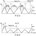
- FIG. 4 is a graph illustrating an example of how the absolute value
- FIG. 5 is a graph illustrating an example of how the absolute value
- of the frequency deviation is a value corresponding to the absolute value of frequency deviation ⁇ fa detected by the direct current interconnection system 1a.
- step S160 namely, T-Th1 ⁇ Tsh
- step S180 namely, T-Th2 ⁇ Tch
- step S160 namely, T-Th1 ⁇ Tsh
- held time th2 is reset. Since the formula shown in step S180 (namely, T-Th2 ⁇ Tch) is not satisfied, mode switching is not performed.
- Direct current interconnection system 1a is operated in the main mode, and the remaining two direct current interconnection systems 1b and 1c are operated in the sub mode.
- the dead band of direct current interconnection system 1a is set as ⁇ 0Hz.
- the dead band of direct current interconnection system 1b is set as ⁇ 2Hz, reference period Tsh thereof is set as one minute, and reference period Tch thereof is set as ten minutes.
- the dead band of direct current interconnection system 1c is set as ⁇ 2Hz, reference period Tsh thereof is set as one minute, and reference period Tch thereof is set as 20 minutes.
- the deviation ⁇ fa between the frequency f ⁇ a detected by frequency detector 4 ⁇ a and the frequency f ⁇ a detected by frequency detector 4 ⁇ a is output from the subtractor 5a and supplied to the dead band filter 6a. Since the dead band of direct current interconnection system 1a is set as ⁇ 0Hz, the frequency deviation ⁇ fa supplied to the dead band filter 6a is supplied to the frequency controller 7a as it is.
- the frequency controller 7a calculates an interchange power correction value ⁇ Pa, which minimizes the frequency deviation ⁇ fa supplied from the dead band filter 6a, and supplies that correction value to the converter controller 8a.
- the converter controller 8a supplies control signal S ⁇ a to the direct current interconnection main circuit 3a in such a manner that the interchange power becomes equal to the total of the interchange power command value Pref and the interchange power correction value ⁇ Pa.
- direct current interconnection system 1b the deviation ⁇ fb between the frequency f ⁇ b detected by frequency detector 4 ⁇ b and the frequency f ⁇ b detected by frequency detector 4 ⁇ b is output from the subtractor 5b.
- direct current interconnection system 1c the deviation ⁇ fc between the frequency f ⁇ c detected by frequency detector 4 ⁇ c and the frequency f ⁇ c detected by frequency detector 4 ⁇ c is output from the subtractor 5c.
- the frequency deviation ⁇ fb detected by the subtractor 5b of direct current interconnection system 1b and the frequency deviation ⁇ fc detected by the subtractor 5c of direct current interconnection system 1c are different in terms of where they are detected. These frequency deviations, however, are frequency deviations of the power systems 2 ⁇ and 2 ⁇ of the same type. Therefore, the frequency deviation ⁇ fb of direct current interconnection system 1b and the frequency deviation ⁇ fc of direct current interconnection system 1c are approximately equal to the frequency deviation ⁇ fa of direct current interconnection system 1a.
- the frequency deviations of the two power systems 2 ⁇ and 2 ⁇ are small (they are within the range of the dead band of ⁇ 2Hz). For this reason, in direct current interconnection system 1b, the frequency deviation ⁇ fb does not pass through the dead band filter 6b. Likewise, in direct current interconnection system 1c, the frequency deviation ⁇ fc does not pass through the dead band filter 6c. As a result, the outputs of the dead band filters 6b and 6c are both zero.
- the frequency controller 7b of direct current interconnection system 1b outputs interchange power correction value ⁇ Pb, which is for minimizing the frequency deviation ⁇ fb, and performs frequency control to suppress the frequency fluctuations.
- the frequency controller 7c of direct current interconnection system 1c outputs interchange power correction value ⁇ Pc, which is for minimizing the frequency deviation ⁇ fc, and performs frequency control to suppress the frequency fluctuations.
- the operating mode of direct current interconnection system 1b switches from the sub mode to the main mode.
- the dead band of the dead band filter 6b of direct current interconnection system 1b changes to ⁇ 0Hz. Since the frequency deviation ⁇ fb is supplied to the frequency controller 7b of direct current interconnection system 1b and frequency control is started, the frequency stops fluctuating.
- two operating modes namely the main mode and the sub mode, are available for each of the direct current interconnection systems 1a to 1c. Since each of the direct current interconnection systems 1a to 1c can be operated in respective modes, it is possible to determine which one of direct current interconnection systems 1a to 1c should be operated in the main mode for frequency control.
- Direct current interconnection systems 1a to 1c are provided with respective dead band filters 6a to 6c to adjust the control amount in frequency control. Owing to this feature, even if the frequency control is performed by two or more direct current interconnection systems 1a to 1c, the control amount in frequency control is prevented from becoming excessive.
- direct current interconnection system 1a operating in the main mode stops for some reason or other, either of direct current interconnection systems 1b and 1c switches from the sub mode to the main mode according to the predetermined priority (which is determined by sensing the frequency fluctuations). Owing to this feature, the frequency control can be continued without pause.
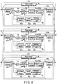
- FIG. 6 illustrates a configuration example of direct current interconnection systems 1Aa, 1Ab and 1Ac according to the second embodiment.
- direct current interconnection system 1Aa Since the three direct current interconnection systems 1Aa-1Ac are similar in configurations, direct current interconnection system 1Aa will be mainly described below, as in the description of the first embodiment.
- Direct current interconnection system 1Aa differs from direct current interconnection system 1a of the first embodiment shown in FIG. 1 , in that frequency controller 10Aa is used in place of frequency controller 10a.
- Frequency controller 10Aa employs a low-pass filter (LPF) 11a and an output switching unit 12a, in place of the dead band filter 6a used in the frequency controller 10a of the first embodiment.
- Direct current interconnection system 1Aa of the second embodiment is similar to direct current interconnection system 1a of the first embodiment in the other points.
- the low-pass filter 11a extracts long-period components (low-frequency components) from the frequency deviation ⁇ fa output from the subtractor 5a.
- the extracted long-period components i.e., long-period components of the frequency deviation ⁇ fa
- the output switching unit 12a receives the frequency deviation ⁇ fa output from the subtractor 5a and the long-period components extracted by the low-pass filter 11a.
- the output switching unit 12a selects either the frequency deviation ⁇ fa received from the subtractor 5a or the long-period components received from the low-pass filter 11a, and supplies the selected one to the frequency controller 7a.
- the output switching unit 12a supplies the frequency deviation ⁇ fa supplied from the subtractor 5a to the frequency controller 7a.
- the output switching unit 12a supplies the long-period components supplied from the low-pass filter 11a to the frequency controller 7a.
- the output switching unit 12 switches outputs in accordance with a result of the determination made by the switching determination unit 93a of the mode switching unit 9a.
- the frequency controller 7a calculates an interchange power correction value ⁇ Pa in order to minimize the frequency deviation ⁇ fa or the long-period components thereof.
- the frequency controller 7a changes the interchange power and controls the frequency in such a manner as to suppress the frequency deviation ⁇ fa.
- the frequency controller 7a performs frequency control in such a manner that the frequency deviation ⁇ fa of the two power systems 2 ⁇ and 2 ⁇ is minimized.
- the frequency controller 7a performs frequency control in such a manner that only the long-period components of the frequency deviation ⁇ fa of the two power systems 2 ⁇ and 2 ⁇ are minimized.
- One of the three direct current interconnection systems 1Aa to 1Ac is operated in the main mode, and the remaining two direct current interconnection systems are operated in the sub mode.
- the frequency controller 7a performs frequency control in such a manner that the frequency deviation ⁇ fa of the two power systems 2 ⁇ and 2 ⁇ is minimized.
- the direct current interconnection systems operated in the sub mode perform frequency control in such a manner that only the long-period components of the frequency deviation ⁇ fa are minimized.
- the direct current interconnection systems 1Aa to 1Ac employ low-pass filters 11a to 11c and output switching units 12a to 12c, in place of the dead band filters 6a to 6c used in the first embodiment.
- the present embodiment provides advantages similar to those of the first embodiment.
- the use of the low-pass filters 11a to 11c prevents the control amount in frequency control from becoming excessive and enables efficient frequency control even if a short-period and sharp frequency fluctuation occurs.
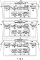
- FIG. 7 illustrates a configuration example of direct current interconnection systems 1Ba, 1Bb and 1Bc according to the third embodiment.
- direct current interconnection system 1Ba Since the three direct current interconnection systems 1Ba-1Bc are similar in configurations, direct current interconnection system 1Ba will be mainly described below, as in the description of the first embodiment.
- Direct current interconnection system 1Ba differs from direct current interconnection system 1a of the first embodiment shown in FIG. 1 , in that frequency controller 10Ba is used in place of frequency controller 10a.
- Frequency controller 10Ba employs a gain setting unit 13a, in place of the dead band filter 6a used in the frequency controller 10a of the first embodiment.
- Direct current interconnection system 1Ba of the third embodiment is similar to direct current interconnection system 1a of the first embodiment in the other points.
- the gain setting unit 13a multiplies the frequency deviation ⁇ fa supplied from subtractor 5a by a predetermined gain, and the frequency deviation ⁇ fa obtained thereby is supplied to the frequency controller 7a.
- the gain setting unit 13a changes the gain in accordance with a result of the determination made by the switching determination unit 93a of the mode switching unit 9a.
- the gain is set as "1." In this case, the frequency deviation ⁇ fa supplied from the subtractor 5a is supplied to the frequency controller 7a as it is.
- the gain is set as "0.” In this case, "0" is supplied to the frequency controller 7a as the frequency deviation ⁇ fa.
- frequency control is not performed in practice.
- the gain used when the operating mode is the sub mode does not have to be “0" unless it is "1."
- the gain may be set as 0.2, and auxiliary frequency control may be performed.
- the direct current interconnection systems 1Ba to 1Bc employ gain setting units 13a to 13c, in place of the dead band filters 6a to 6c used in the first embodiment.
- the present embodiment provides advantages similar to those of the first embodiment.
- the gains of the gain setting units 13a to 13c are set as "0" when the operating mode is the sub mode. By setting the gains in this manner, one of direct current interconnection systems 1Ba to 1Bc that is operated in the main mode performs frequency control, and the remaining direct current interconnection systems operated in the sub mode do not perform frequency control.
- the gains of the gain setting units 13a to 13c are set as a value greater than "0" and less than 1.
- the direct current interconnection systems operated in the sub mode perform auxiliary frequency control such that the control amount in frequency control does not become excessive.
- FIG. 8 illustrates a configuration example of direct current interconnection systems 1Ca, 1Cb and 1Cc according to the fourth embodiment.
- direct current interconnection system 1Ca Since direct current interconnection systems 1Ca-1Cc are similar in configurations, direct current interconnection system 1Ca will be mainly described below, as in the description of the first embodiment.
- Direct current interconnection system 1Ca differs from direct current interconnection system 1a of the first embodiment shown in FIG. 1 , in that frequency controller 10Ca is used in place of frequency controller 10a.
- Frequency controller 10Ca employs an allocation processor (interchange power allocator) 14a in place of the dead band filter 6a and mode switching unit 9a used in the frequency controller 10a of the first embodiment, and also employs frequency controller 7Ca in place of frequency controller 7a.
- Direct current interconnection system 1Ca of the fourth embodiment is similar to direct current interconnection system 1a of the first embodiment in the other points.
- the frequency deviation ⁇ fa calculated by the subtractor 5a is supplied to the frequency controller 7Ca as it is.
- the frequency controller 7Ca calculates an interchange power correction value ⁇ P on the basis of the frequency deviation ⁇ fa.
- the calculated interchange power correction value ⁇ P is an overall correction value and enables each of the direct current interconnection systems 1Ca to 1Cc to perform frequency control.
- the frequency controller 7Ca supplies the calculated interchange power correction value ⁇ P to the allocation processor 14a. In the other points, the frequency controller 7Ca is similar to frequency controller 7a of the first embodiment.
- the allocation processors 14a to 14c of the three direct current interconnection systems 1Ca to 1Cc are connected to one another on an information transmission path.
- Distribution processor 14a calculates an interchange power correction value ⁇ Pa handled by direct current interconnection system 1Ca, based on either the interchange power correction value ⁇ P calculated by frequency controller 7Ca or the interchange power correction values entered from the allocation processors 14b and 14c of the other direct current interconnection systems 1Cb and 1Cc.
- allocation processor 14a provides direct current interconnection systems 1Cb and 1Cc operating in the sub mode with their corresponding interchange power correction values.
- direct current interconnection system 1Ca has the highest priority
- direct current interconnection system 1Cb has an intermediate priority
- direct current interconnection system 1Cc has the lowest priority.
- the control amount in frequency control of a higher-priority direct current interconnection system is larger than that of a lower-priority direct current interconnection system. Based on this priority, the initial settings of the direct current interconnection systems 1Ca to 1Cc are determined as follows:
- the operating mode of direct current interconnection system 1Cb is the sub mode.
- Direct current interconnection system 1Cb performs frequency control in response to a command supplied from higher-priority direct current interconnection system 1Ca.
- the operating mode of direct current interconnection system 1Cc is the sub mode.
- Direct current interconnection system 1Cc performs frequency control in response to a command supplied from one of higher-priority direct current interconnection systems 1Ca and 1Cb.
- Allocation processor 14a of direct current interconnection system 1Ca operating in the main mode calculates an interchange power correction value ⁇ Pa handled by direct current interconnection system 1Ca, based on the overall interchange power correction value ⁇ P calculated by frequency controller 7Ca.
- allocation processor 14a calculates the overall interchange power correction value ⁇ P as interchange power correction value ⁇ Pa handled by direct current interconnection system 1Ca.
- allocation processor 14a calculates an interchange power correction value corresponding to a first power value of the overall interchange power correction value ⁇ P, as interchange power correction value ⁇ Pa handled by direct current interconnection system 1Ca. Allocation processor 14a allocates the remaining interchange power correction value to direct current interconnection systems 1Cb and 1Cc as an interchange power correction value to be handled by them.
- the interchange power correction value ⁇ Pa handled by direct current interconnection system 1Ca is supplied to the converter controller 8a.
- allocation processor 14a determines that it should be handled by direct current interconnection system 1Cb having the next high priority, and supplies it to direct current interconnection system 1Cb as interchange power correction value ⁇ Pb, provided that it does not exceed a predetermined second power value (e.g., the rated power of direct current interconnection main circuit 3b of direct current interconnection system 1Cb).
- a predetermined second power value e.g., the rated power of direct current interconnection main circuit 3b of direct current interconnection system 1Cb.
- allocation processor 14a determines that the remaining interchange power correction value should be handled by direct current interconnection system 1Cc having the next high priority, and supplies it to direct current interconnection system 1Cc as interchange power correction value ⁇ Pc, provided that it does not exceed a predetermined third power value (e.g., the rated power of direct current interconnection main circuit 3c of direct current interconnection system 1Cc).
- a predetermined third power value e.g., the rated power of direct current interconnection main circuit 3c of direct current interconnection system 1Cc.
- Distribution processor 14a supplies the calculated interchange power correction values ⁇ Pb and ⁇ Pc to allocation processors 14b and 14c corresponding to them.
- Distribution processor 14b supplies interchange power correction value ⁇ Pb (which should be handled by direct current interconnection system 1Cb) to converter controller 8b.
- Distribution processor 14c supplies interchange power correction value ⁇ Pc (which should be handled by direct current interconnection system 1Cc) to converter controller 8c.
- Interchange power correction value ⁇ P may be allocated to direct current interconnection systems 1Ca to 1Cc in a method different from that described above. For example, interchange power correction value ⁇ P may be divided equally and these divisions may be allocated to direct current interconnection systems 1Ca to 1Cc. Alternatively, interchange power correction value ⁇ P may be allocated in proportions determined by the rated power of direct current interconnection main circuits 3a to 3c.
- the allocation processor 14b of direct current interconnection system 1Cb operating in the sub mode fails to receive interchange power correction value ⁇ Pb to be handled by direct current interconnection system 1Cb.
- the allocation processor 14c of direct current interconnection system 1Cc operating in the sub mode fails to receive interchange power correction value ⁇ Pc to be handled by direct current interconnection system 1Cc.
- Non-signal duration times are predetermined for the allocation processors 14b and 14c.
- the non-signal duration time is determined such that the higher the priority of a direct current interconnection system is, the shorter will be the corresponding non-signal duration time.
- the non-signal duration time of allocation processor 14b is set as 10 minutes and the non-signal duration time of allocation processor 14c is set as 20 minutes.
- allocation processor 14b switches the operating mode of direct current interconnection system 1Cb from the sub mode to the main mode.
- allocation processor 14b calculates interchange power correction value ⁇ Pb to be handled by direct current interconnection system 1Cb and interchange power correction value ⁇ Pc to be handled by direct current interconnection system 1Cc, on the basis of the overall interchange power correction value ⁇ P calculated by frequency controller 7Cb.
- Distribution processor 14b supplies the calculated interchange power correction value ⁇ Pc to allocation processor 14c.
- allocation processor 14c After 10 minutes (non-signal duration time) elapse from the time when allocation processor 14c stops receiving interchange power correction value ⁇ Pc (which is to be handled by direct current interconnection system 1Cc) from allocation processor 14a and before 20 minutes (non-signal duration time) elapse, allocation processor 14c receives interchange power correction value ⁇ Pc to be handled by direct current interconnection system 1Cc from allocation processor 14b. Therefore, even if direct current interconnection system 1Ca stops, allocation processor 14c does not switch the operating mode of direct current interconnection system 1Cc from the sub mode to the main mode.
- allocation processor 14c switches the operating mode of direct current interconnection system 1Cc from the sub mode to the main mode.
- allocation processors 14b and 14c switch operating modes by detecting that the reception of interchange power correction values ⁇ Pb and ⁇ Pc to be handled by direct current interconnection systems 1Cb and 1Cc are not received.
- the operating modes may be switched in other methods.
- allocation processors 14a to 14c may switch operating modes by mutually communicating with each other at all times and detecting that direct current interconnection systems 1Ca to 1Cc stop operations (or stop communications).
- all direct current interconnection systems 1Ca to 1Cc are provided with their respective allocation processors 14a to 14c, and a direct current interconnection system operating in the main mode can calculate interchange power correction values ⁇ Pa to ⁇ Pc to be allocated to all direct current interconnection systems 1Ca to 1Cc.
- the present embodiment can provide advantages similar to those of the first embodiment.
- the number of direct current interconnection systems is three.
- the number of direct current interconnection systems may be any number as long as it is two or more.
- a particular frequency deviation (hereinafter a specific frequency deviation) that satisfies predetermined conditions is extracted from the frequency deviations of the two power systems, by using a dead band filter, a unit filter or a gain setting unit, and frequency control is performed in such a manner as to minimize that specific frequency deviation.
- the extraction method of the specific frequency deviation is not limited to this.
- a specific frequency deviation may be extracted from the frequency deviations of the two power systems under any condition (components or range).
Landscapes
- Engineering & Computer Science (AREA)
- Power Engineering (AREA)
- Inverter Devices (AREA)
- Supply And Distribution Of Alternating Current (AREA)
Abstract
Description
- The present invention relates to a frequency control apparatus for a direct current interconnection system, and to a direct current interconnection system.
- There is technology that individually measures the operating condition of an inverter-incorporated electric instrument used at home. Instead of installing a measuring instrument for each electric instrument, the technology estimates the operating condition of each electric instrument in a non-invasive manner by measuring how each electric instrument operates based on the condition of the incoming line from an electric pole to a house.
- The technology pays special attention to the fundamental waves generated by electric instruments and harmonic currents and the phases corresponding to the voltages, and applies a neural network. Based on the measurement data on voltages and currents measured in the neighborhood of the lead-in port of the feeding line, the technology individually estimates the operating condition of each electric instrument.
- An apparatus for reliably checking the ON/OFF operation of an electric instrument and estimating the type of electric instrument in the loaded condition is also known in the art. The apparatus detects which electric instrument is in the loaded condition from among a plurality of electric instruments located downstream of a measurement point and connected through a switch means and estimates the type of electric instrument in the loaded condition, based on the electricity quantity detection results at the measuring point.
- An instrument condition detector is also known in the art, which accurately detects the operating conditions of electric instruments with no need to learn the combinations of operating conditions of electric instruments to be detected.
- The instrument condition detector calculates the feature amount of each frequency component based on the measurements of currents and voltages. To identify an electric instrument, the instrument condition detector searches a database in which identification information for identifying electric instruments, feature amounts and operating conditions are associated with one another. The instrument condition detector compares calculated feature amounts with the feature amounts stored in the database, determines whether the calculated feature amounts are identical to those stored in the database, and identifies the electric instruments based on the determination.
- However, no consideration is given to the case where two power systems are interconnected by a plurality of direct current interconnection systems having a frequency control function, and the following problems occur.
- Where the frequency deviation of the two power systems is minimized by power interchange, a change (correction value) of the required interchange power is determined in accordance with the frequency deviation. The change of the required interchange power has to be equal to the total sum of the interchange powers of the direct current interconnection systems.
- However, where the direct current interconnection systems have different system frequency control functions and determine a change of interchange power based on the frequency deviation, the total value of the changes of interchange power exceeds the actually required change of interchange power, resulting in excessive control. In this case, frequency fluctuations may worsen.
- If the changes of interchange power calculated by the direct current interconnection systems are adjusted to be small values in accordance with the number of direct current interconnection systems, the total value of the changes of interchange power may be small, if some of the direct current interconnection systems stop. As a result, the frequency control effect is affected, accordingly.
- Under the circumstances, there is a demand for a frequency control apparatus for a direct current interconnection system and a direct current interconnection system, which are capable of effectively suppressing the frequency fluctuations of power systems when the power systems are interconnected by a plurality of direct current interconnection systems.
-
- [Patent Literature 1]
Jpn. Pat. Appln. KOKAI Publication No.10-224994 - [Patent Literature 2]
Jpn. Pat. Appln. KOKAI Publication No.2011-223714 - [Patent Literature 3]
Jpn. Pat. Appln. KOKAI Publication No.2011-223715 - A frequency control apparatus according to an embodiment is a frequency control apparatus for a plurality of direct current interconnection systems which interconnect two power systems and control frequencies. The frequency control apparatus includes: a frequency deviation detector for detecting frequency deviations of the two power systems, a specific frequency deviation extractor for extracting a specific frequency deviation satisfying a predetermined condition from the frequency deviations detected by the frequency deviation detector; and a control switching unit for switching from frequency control which interchanges power between the two power systems in such a manner as to minimize the specific frequency deviation extracted by the specific frequency deviation extractor to frequency control which interchanges power between the two power systems in such a manner as to minimize the frequency deviation detected by the frequency deviation detector.
-
-
FIG. 1 illustrates a configuration example of direct current interconnection systems according to the first embodiment; -
FIG. 2 illustrates a configuration example of the direct current interconnection main circuit and converter controller of the first embodiment; -
FIG. 3 is a flowchart illustrating an example of a process by which the switching determination unit of the first embodiment performs mode switching; -
FIG. 4 is a graph illustrating an example of how the absolute value of a frequency deviation varies when the switching determination unit of the first embodiment performs mode switching; -
FIG. 5 is a graph illustrating an example of how the absolute value of a frequency deviation fluctuates when the switching determination unit of the first embodiment does not perform mode switching; -
FIG. 6 illustrates a configuration example of direct current interconnection systems according to the second embodiment; -
FIG. 7 illustrates a configuration example of direct current interconnection systems according to the third embodiment; and -
FIG. 8 illustrates a configuration example of direct current interconnection systems according to the fourth embodiment. - Mode for Carrying Out the Invention Embodiments of the present invention will now be described with reference to the accompanying drawings.
-
FIG. 1 illustrates a configuration example of directcurrent interconnection systems - Two power systems 2α and 2β are interconnected by three direct
current interconnection systems - Direct
current interconnection system 1a comprises a direct current interconnectionmain circuit 3a and afrequency control apparatus 10a. Thefrequency control apparatus 10a includes two frequency detectors 4αa and 4βa, and further includes a subtractor (frequency deviation detector) 5a, a dead band filter (specific frequency deviation extractor) 6a, afrequency controller 7a, aconverter controller 8a and a mode switching unit (control switching unit) 9a. - Direct
current interconnection system 1b comprises a direct current interconnectionmain circuit 3b and afrequency control apparatus 10b. Thefrequency control apparatus 10b includes two frequency detectors 4αb and 4βb, and further includes asubtractor 5b, adead band filter 6b, afrequency controller 7b, aconverter controller 8b and amode switching unit 9b. - Direct
current interconnection system 1c comprises a direct current interconnectionmain circuit 3c and afrequency control apparatus 10c. Thefrequency control apparatus 10c includes two frequency detectors 4αc and 4βc, and further includes asubtractor 5c, adead band filter 6c, afrequency controller 7c, aconverter controller 8c and amode switching unit 9c. - Since the three direct
current interconnection systems 1a-1c are similar in configurations, directcurrent interconnection system 1a will be mainly described below. With respect to the other two directcurrent interconnection systems current interconnection system 1a. -
FIG. 2 illustrates a configuration example of the direct current interconnectionmain circuit 3a andconverter controller 8a of the first embodiment. - The direct current interconnection
main circuit 3a includes two converters 31αa and 31βa, two transformer 32αa and 32βa for converters, a directcurrent reactor 33a, adirect current detector 34, and aDC voltage detector 35. - The two converters 31αa and 31βa are a pair of converters, one (31αa) of which performs ac-to-dc voltage conversion and the other (31βa) performs dc-to-ac voltage conversion. The two converters 31αa and 31βa are connected to each other as a DC circuit, with the direct
current reactor 33a interposed therebetween. Converter 31αa for dc-to-ac voltage conversion is connected to power system 2α by way of conversion transformer 32αa. Converter 31βa for dc-to-ac voltage conversion is connected to power system 2β by way of conversion transformer 32βa. - The direct
current detector 34 and theDC voltage detector 35 are provided in the DC circuit. The directcurrent detector 34 detects direct current Idc flowing through the DC circuit and outputs a detection result to theconverter controller 8a. TheDC voltage detector 35 detects direct current Edc flowing through the DC circuit and outputs a detection result to theconverter controller 8a. - The
converter controller 8a comprises anadder 81a, a current commandvalue operation unit 82a,subtractor 83a, a directcurrent controller 84a,subtractor 85a, and aDC voltage controller 86a. - The
adder 81a receives interchange power command value Pref and also receives interchange power correction value ΔPa calculated byfrequency controller 7a and handled by directcurrent interconnection system 1a. The interchange power command value Pref is provided by an upper-level system such as a feeding power direction center. - The
adder 81a adds the interchange power correction value ΔPa to the interchange power command value Pref, and supplies interchange power command value Pref1 obtained thereby by this addition to the current commandvalue operation unit 82a. The current commandvalue operation unit 82a calculates a direct current command value Idcref so that the interchange power can satisfy the interchange power command value Pref1, and supplies the calculated direct current command value Idcref tosubtractor 83a. - Subtractor 83a receives the direct current command value Idcref calculated by the current command
value operation unit 82a and a direct current Idc detected by the directcurrent detector 34. Subtractor 83a subtracts the direct current command value Idcref from the direct current Idc, and supplies the resultant difference to the directcurrent controller 84a. - Based on the direct current difference output from the
subtractor 83a, the directcurrent controller 84a supplies a control command Sαa to the converter 31αa of the direct current interconnectionmain circuit 3a. The control command Sαa is used for controlling the output of the converter 31αa so that the direct current Idc can become equal to the direct current command value Idcref. The converter 31αa performs ac-to-dc voltage conversion in accordance with the control command Sαa. - Subtractor 85a receives a rated voltage value Edcref of the DC circuit, and also receives a DC voltage Edc detected by the
DC voltage detector 35. Subtractor 85a subtracts the DC voltage EDc from the rated voltage value Edcref, and supplies the resultant difference to theDC voltage controller 86a. - Based on the DC voltage difference received from
subtractor 85a, theDC voltage controller 86a supplies a control command Sβa to the converter 31βa of the direct current interconnectionmain circuit 3a. The control command Sβa is used for controlling the output of the converter 31βa so that the DC voltage Edc can become equal to the rated voltage value Edcref. The converter 31βa performs dc-to-ac voltage conversion in accordance with the control command Sβa. - As described above, the
converter controller 8a interchanges power between the two power systems 2α and 2β by controlling the two converters 31αa and 31βa of the direct current interconnectionmain circuit 3a. For example, when the frequency fαa of power system 2α increases, the sum of the interchange power command value Pref and the interchange power correction value ΔPa increases. Accordingly, the power provided from power system 2α to power system 2β increases. Since the surplus power of power system 2α decreases, the frequency increase is suppressed. - Frequency detector 4αa detects frequency fαa of the voltage of power system 2α. Frequency detector 4βa detects frequency fβa of the voltage of power system 2β. Frequency detector 4αa supplies the detected frequency fαa to
subtractor 5a. Frequency detector 4βa supplies the detected frequency fβa tosubtractor 5a. - Subtractor 5a calculates the difference (frequency deviation) between the two frequencies (Δfa=fαa-fβa). Subtractor 5a supplies the calculated frequency deviation Δfa to both the
dead band filter 6a and themode switching unit 9a. - The frequency deviation Δfa supplied from
subtractor 5a is made to pass through thedead band filter 6a (the dead frequency band of which is predetermined), and the resultant frequency deviation Δfa is supplied to thefrequency controller 7a. If the frequency deviation Δfa is within the predetermined dead band, the output of thedead band filter 6a is zero. If the frequency deviation Δfa is outside the predetermined dead band, the frequency deviation Δfa received fromsubtractor 5a is output from thedead band filter 6a as it is. - The
frequency controller 7a calculates an interchange power correction value ΔPa in accordance with the frequency deviation Δfa supplied from thedead band filter 6a. Thefrequency controller 7a is made, for example, of a comparison circuit. The interchange power correction value ΔPa calculated byfrequency controller 7a is a correction value handled by directcurrent interconnection system 1a. Thefrequency controller 7a supplies the calculated interchange power correction value ΔPa to theconverter controller 8a. Based on this correction value, power is interchanged between the two converters 31αa and 31βa in such a manner that the frequency deviation Δfa is minimized (becomes closer to zero). - Based on the frequency deviation Δfa supplied from the
subtractor 5a, themode switching unit 9a switches the operation mode of the directcurrent interconnection system 1a between a main mode and a sub mode. The main mode is an operation mode which plays a central role in the frequency control when the three directcurrent interconnection systems 1a to 1c are operated. The sub mode is an operation mode which plays a peripheral role in the frequency control when the three direct current interconnection systems are operated. - Of the three direct
current interconnection systems 1a to 1c, at least one of them is operated in the main mode. With respect to the direct current interconnection systems operated in the sub mode, the number of such systems may be any number or zero. If a direct current interconnection system operating in the main mode fails to operate properly for some reason or other, themode switching unit 9a performs control so that another direct current interconnection system can take over the function of the main mode. - The
mode switching unit 9a includes afluctuation detector 91a, alevel detector 92a and a switchingdetermination unit 93a. - The
fluctuation detector 91a receives a frequency deviation Δfa supplied from thesubtractor 5a. Thefluctuation detector 91a extracts a fluctuation component from the received frequency deviation Δfa. Thefluctuation detector 91a is made, for example, of an incomplete differentiator. Thefluctuation detector 91a supplies the extracted fluctuation component of the frequency deviation Δfa to thelevel detector 92a. - The
level detector 92a receives the fluctuation component of the frequency deviation Δfa, which is extracted by thefluctuation detector 91a. If the absolute value of the fluctuation component of the frequency deviation Δfa is equal to or more than a predetermined threshold, thelevel detector 92a supplies "1" to the switchingdetermination unit 93a. If that absolute value is less than the predetermined threshold, thelevel detector 92a supplies "0" to the switchingdetermination unit 93a. - Two reference times Tsh and Tch are predetermined for the switching
determination unit 93a. Reference time Tsh is a time used for determining whether or not the fluctuation in the frequency deviation Δfa is frequent. Reference time Tsh is, for example, one minute. - Reference time Tch is a time used for determining whether the fluctuation in the frequency deviation Δfa continues for a long time. Reference time Tch is, for example, 10 minutes or 20 minutes. Reference time Tch differs, depending upon the direct
current interconnection systems 1a to 1c. Short reference time Tch is determined for a direct current interconnection system which is switched to the main mode in preference to others. - A value output from the
level detector 92a is received by the switchingdetermination unit 93a as value Ans. The switchingdetermination unit 93a determines whether or not to perform mode switching, based on value Ans and the predetermined two reference times Tsh and Tch. The criterion for determining whether the mode should be switched from the sub mode to the main mode is based on the detection of whether or not the state in which "1" is frequently output from thelevel detector 92a due to the fluctuation in the frequency deviation Δfa continues for more than a certain time. - The switching
determination unit 93a switches operation modes by changing the range of the dead band of thedead band filter 6a. When the operation mode is switched from the sub mode to the main mode, the switchingdetermination unit 93a changes the dead band of thedead band filter 6a to ± 0Hz. Conversely, when the operation mode is switched from the main mode to the sub mode, the switchingdetermination unit 93a changes the dead band of thedead band filter 6a to a range other than ± 0Hz (e.g., ± 2Hz). - How the switching
determination unit 93a determines the mode switching from the sub mode to the main mode will be described with reference toFIG. 3. FIG. 3 is a flowchart illustrating an example of a process by which the switching determination unit of the first embodiment performs mode switching. - The switching
determination unit 93a determines that a value it receives from thelevel detector 92a is value Ans (Step S110). Where value Ans is "1" (Yes in Step 120), the switchingdetermination unit 93a stores current time T as held time Th1 (step S130), and the flow advances to the determination processing of step S140. Where value Ans is "0" (No in Step S120), the switchingdetermination unit 93a advances to the determination processing of step S160. - In the determination processing of step S140, the switching
determination unit 93a determines whether held time Th2 has been reset or not. Where held time Th2 has been reset (Yes in Step 140), the switchingdetermination unit 93a stores current time T as held time Th2 (step S150), and the flow advances to the determination processing of step S160. The initial state of held time Th2 is a reset state. Where held time Th2 has not been reset (No in Step 140), the switchingdetermination unit 93a advances to the processing of step S160. - In the determination processing of step S160, the switching
determination unit 93a determines whether or not the period from the time stored as held time Th1 to current time T is equal to or longer than reference period Tsh (e.g., one minute). - If the period from the time stored as held time Th1 to current time T is equal to or longer than reference period Tsh (Yes in step S160), the switching
determination unit 93a resets the held time Th2 by storing a maximal value as time Th2 (step S170). - After resetting time Th2 (step S170), the switching
determination unit 93a advances to the determination processing of step S180. If the period from the time stored as held time Th1 to current time T is shorter than reference period Tsh (No in step S160), the switchingdetermination unit 93a advances to the determination processing of step S180. - In the determination processing of step S180, the switching
determination unit 93a determines whether or not the period from the time stored as held time Th2 to current time T is equal to or longer than reference period Tch (e.g., ten minutes) (step S180). If held time Th2 is reset in step S170, the maximal value is stored as held time Th2, so that the determination never fails to be false (No). - If the period from the time stored as held time Th2 to current time T is equal to or longer than reference period Tch (Yes in step S180), the switching
determination unit 93a executes mode switching from the sub mode to the main mode (step S190). On the other hand, if the period from the time stored as held time Th2 to current time T is shorter than reference period Tch (No in step S180), the switchingdetermination unit 93a returns to the processing of step S110, and a series of operations mentioned above are repeated. - How the switching
determination unit 93a performs the mode switching from the sub mode to the main mode will be described with reference toFIGS. 3 ,4 and 5. FIG. 4 is a graph illustrating an example of how the absolute value |Δf| of a frequency deviation varies when the switchingdetermination unit 93a of the first embodiment performs mode switching.FIG. 5 is a graph illustrating an example of how the absolute value |Δf| of a frequency deviation fluctuates when the switchingdetermination unit 93a of the first embodiment does not perform mode switching. The absolute value |Δf| of the frequency deviation is a value corresponding to the absolute value of frequency deviation Δfa detected by the directcurrent interconnection system 1a. - If the absolute value |Δf| of the frequency deviation fluctuates greatly, as shown in
FIG. 4 , this absolute value frequently exceeds the threshold of thelevel detector 92a, so that held time Th1 is updated at short intervals. Accordingly, the formula shown in step S160 (namely, T-Th1≧Tsh) is not satisfied. - Therefore, held time Th2 is not reset, and the period from this held time Th2 to current time T increases. As a result, the formula shown in step S180 (namely, T-Th2≧Tch) is satisfied, and mode switching is carried out.
- On the other hand, if the absolute value |Δf| of the frequency deviation does not greatly fluctuate, as shown in
FIG. 5 , this absolute value hardly exceeds the threshold of thelevel detector 92a, so that held time Th1 is updated at long intervals. Accordingly, the formula shown in step S160 (namely, T-Th1≧Tsh) is satisfied. As a result, held time th2 is reset. Since the formula shown in step S180 (namely, T-Th2≧Tch) is not satisfied, mode switching is not performed. - Specific operations of the three direct
current interconnection systems 1a to 1c will be described with reference toFIG. 1 . - It is assumed here that the three direct
current interconnection systems 1a to 1c are set as follows: Directcurrent interconnection system 1a is operated in the main mode, and the remaining two directcurrent interconnection systems - The dead band of direct
current interconnection system 1a is set as ±0Hz. The dead band of directcurrent interconnection system 1b is set as ±2Hz, reference period Tsh thereof is set as one minute, and reference period Tch thereof is set as ten minutes. The dead band of directcurrent interconnection system 1c is set as ±2Hz, reference period Tsh thereof is set as one minute, and reference period Tch thereof is set as 20 minutes. - In direct
current interconnection system 1a, the deviation Δfa between the frequency fαa detected by frequency detector 4αa and the frequency fβa detected by frequency detector 4βa is output from thesubtractor 5a and supplied to thedead band filter 6a. Since the dead band of directcurrent interconnection system 1a is set as ±0Hz, the frequency deviation Δfa supplied to thedead band filter 6a is supplied to thefrequency controller 7a as it is. - The
frequency controller 7a calculates an interchange power correction value ΔPa, which minimizes the frequency deviation Δfa supplied from thedead band filter 6a, and supplies that correction value to theconverter controller 8a. Theconverter controller 8a supplies control signal Sαa to the direct current interconnectionmain circuit 3a in such a manner that the interchange power becomes equal to the total of the interchange power command value Pref and the interchange power correction value ΔPa. - Accordingly, if the interchange power varies by interchange power correction value ΔPa, both frequency fαa of power system 2α and frequency fβa of power system 2β change, and frequency deviation Δfa newly detected after that change passes through the
dead band filter 6a and is supplied to thefrequency controller 7a. In this manner, the interchange power correction value ΔPa is updated, and the interchange power is varied repeatedly. As a result, the frequency deviation Δfa converges to a minimal value. - In the meantime, in direct
current interconnection system 1b, the deviation Δfb between the frequency fαb detected by frequency detector 4αb and the frequency fβb detected by frequency detector 4βb is output from thesubtractor 5b. In directcurrent interconnection system 1c, the deviation Δfc between the frequency fαc detected by frequency detector 4αc and the frequency fβc detected by frequency detector 4βc is output from thesubtractor 5c. - The frequency deviation Δfb detected by the
subtractor 5b of directcurrent interconnection system 1b and the frequency deviation Δfc detected by thesubtractor 5c of directcurrent interconnection system 1c are different in terms of where they are detected. These frequency deviations, however, are frequency deviations of the power systems 2α and 2β of the same type. Therefore, the frequency deviation Δfb of directcurrent interconnection system 1b and the frequency deviation Δfc of directcurrent interconnection system 1c are approximately equal to the frequency deviation Δfa of directcurrent interconnection system 1a. - At normal times, the frequency deviations of the two power systems 2α and 2β are small (they are within the range of the dead band of ± 2Hz). For this reason, in direct
current interconnection system 1b, the frequency deviation Δfb does not pass through thedead band filter 6b. Likewise, in directcurrent interconnection system 1c, the frequency deviation Δfc does not pass through thedead band filter 6c. As a result, the outputs of thedead band filters - Since the interchange power correction value ΔPb output from
frequency controller 7b and the interchange power correction value ΔPc output fromfrequency controller 7c are both zero, the two directcurrent interconnection systems - Let us assume that a disturbance occurs in the two power systems 2α and 2β and their frequencies fluctuate greatly, and that the frequency deviation Δfb of direct
current interconnection system 1b exceeds the dead band of thedead band filter 6b and the frequency deviation Δfc of directcurrent interconnection system 1c exceeds the dead band of thedead band filter 6c. - In such a case, the
frequency controller 7b of directcurrent interconnection system 1b outputs interchange power correction value ΔPb, which is for minimizing the frequency deviation Δfb, and performs frequency control to suppress the frequency fluctuations. Likewise, thefrequency controller 7c of directcurrent interconnection system 1c outputs interchange power correction value ΔPc, which is for minimizing the frequency deviation Δfc, and performs frequency control to suppress the frequency fluctuations. - A description will now be given of the case where direct
current interconnection system 1a stops. - If direct
current interconnection system 1a stops, the frequency deviation Δfb detected in directcurrent interconnection system 1b and the frequency deviation Δfc detected in directcurrent interconnection system 1c increase. - If the frequency deviation Δfb of direct
current interconnection system 1b increases and this state continues for more than 10 minutes, which is reference period Tch set for the switchingdetermination unit 93b of directcurrent interconnection system 1b, then the operating mode of directcurrent interconnection system 1b switches from the sub mode to the main mode. In other words, the dead band of thedead band filter 6b of directcurrent interconnection system 1b changes to ±0Hz. Since the frequency deviation Δfb is supplied to thefrequency controller 7b of directcurrent interconnection system 1b and frequency control is started, the frequency stops fluctuating. - When the frequency stops fluctuating, the frequency deviation Δfc of direct
current interconnection system 1c becomes closer to zero. Therefore, even if directcurrent interconnection system 1a stops, the operating mode of directcurrent interconnection system 1b switches to the main mode, and the above-mentioned state does not continue for more than 20 minutes, which is reference period Tch set for the switchingdetermination unit 93c of directcurrent interconnection system 1c. Therefore, the operating mode of directcurrent interconnection system 1c, which has lower priority than that of directcurrent interconnection system 1b, remains in the sub mode. - According to the present embodiment, two operating modes, namely the main mode and the sub mode, are available for each of the direct
current interconnection systems 1a to 1c. Since each of the directcurrent interconnection systems 1a to 1c can be operated in respective modes, it is possible to determine which one of directcurrent interconnection systems 1a to 1c should be operated in the main mode for frequency control. - Direct
current interconnection systems 1a to 1c are provided with respectivedead band filters 6a to 6c to adjust the control amount in frequency control. Owing to this feature, even if the frequency control is performed by two or more directcurrent interconnection systems 1a to 1c, the control amount in frequency control is prevented from becoming excessive. - At normal times when the frequency fluctuations are small, the control amount of the frequency control performed by direct
current connection systems 1a to 1c is kept from being excessive, and the frequency fluctuations do not worsen. - If a disturbance occurring in the power systems 2α and 2β results in great frequency fluctuations, two or more direct current interconnection systems perform the frequency control. Accordingly, reliable frequency control is enabled.
- Furthermore, if direct
current interconnection system 1a operating in the main mode stops for some reason or other, either of directcurrent interconnection systems -
FIG. 6 illustrates a configuration example of direct current interconnection systems 1Aa, 1Ab and 1Ac according to the second embodiment. - Since the three direct current interconnection systems 1Aa-1Ac are similar in configurations, direct current interconnection system 1Aa will be mainly described below, as in the description of the first embodiment.
- Direct current interconnection system 1Aa differs from direct
current interconnection system 1a of the first embodiment shown inFIG. 1 , in that frequency controller 10Aa is used in place offrequency controller 10a. Frequency controller 10Aa employs a low-pass filter (LPF) 11a and anoutput switching unit 12a, in place of thedead band filter 6a used in thefrequency controller 10a of the first embodiment. Direct current interconnection system 1Aa of the second embodiment is similar to directcurrent interconnection system 1a of the first embodiment in the other points. - The low-
pass filter 11a extracts long-period components (low-frequency components) from the frequency deviation Δfa output from thesubtractor 5a. The extracted long-period components (i.e., long-period components of the frequency deviation Δfa) are supplied from the low-pass filter 11a to theoutput switching unit 12a. - The
output switching unit 12a receives the frequency deviation Δfa output from thesubtractor 5a and the long-period components extracted by the low-pass filter 11a. Theoutput switching unit 12a selects either the frequency deviation Δfa received from thesubtractor 5a or the long-period components received from the low-pass filter 11a, and supplies the selected one to thefrequency controller 7a. - Where direct current interconnection system 1Aa is operated in the main mode, the
output switching unit 12a supplies the frequency deviation Δfa supplied from thesubtractor 5a to thefrequency controller 7a. Where direct current interconnection system 1Aa is operated in the sub mode, theoutput switching unit 12a supplies the long-period components supplied from the low-pass filter 11a to thefrequency controller 7a. The output switching unit 12 switches outputs in accordance with a result of the determination made by the switchingdetermination unit 93a of themode switching unit 9a. - As in the first embodiment, the
frequency controller 7a calculates an interchange power correction value ΔPa in order to minimize the frequency deviation Δfa or the long-period components thereof. In accordance with the interchange power correction value ΔPa, thefrequency controller 7a changes the interchange power and controls the frequency in such a manner as to suppress the frequency deviation Δfa. - Where direct current interconnection system 1Aa is operated in the main mode, the
frequency controller 7a performs frequency control in such a manner that the frequency deviation Δfa of the two power systems 2α and 2β is minimized. Where direct current interconnection system 1Aa is operated in the sub mode, thefrequency controller 7a performs frequency control in such a manner that only the long-period components of the frequency deviation Δfa of the two power systems 2α and 2β are minimized. - One of the three direct current interconnection systems 1Aa to 1Ac is operated in the main mode, and the remaining two direct current interconnection systems are operated in the sub mode. Where direct current interconnection system 1Aa is operated in the main mode, the
frequency controller 7a performs frequency control in such a manner that the frequency deviation Δfa of the two power systems 2α and 2β is minimized. The direct current interconnection systems operated in the sub mode perform frequency control in such a manner that only the long-period components of the frequency deviation Δfa are minimized. - According to the present embodiment, the direct current interconnection systems 1Aa to 1Ac employ low-
pass filters 11a to 11c andoutput switching units 12a to 12c, in place of thedead band filters 6a to 6c used in the first embodiment. With this configuration, the present embodiment provides advantages similar to those of the first embodiment. - Even where the frequency control is performed by two or more direct current interconnection systems 1Aa to 1Ac, the use of the low-
pass filters 11a to 11c prevents the control amount in frequency control from becoming excessive and enables efficient frequency control even if a short-period and sharp frequency fluctuation occurs. -
FIG. 7 illustrates a configuration example of direct current interconnection systems 1Ba, 1Bb and 1Bc according to the third embodiment. - Since the three direct current interconnection systems 1Ba-1Bc are similar in configurations, direct current interconnection system 1Ba will be mainly described below, as in the description of the first embodiment.
- Direct current interconnection system 1Ba differs from direct
current interconnection system 1a of the first embodiment shown inFIG. 1 , in that frequency controller 10Ba is used in place offrequency controller 10a. Frequency controller 10Ba employs again setting unit 13a, in place of thedead band filter 6a used in thefrequency controller 10a of the first embodiment. Direct current interconnection system 1Ba of the third embodiment is similar to directcurrent interconnection system 1a of the first embodiment in the other points. - The
gain setting unit 13a multiplies the frequency deviation Δfa supplied fromsubtractor 5a by a predetermined gain, and the frequency deviation Δfa obtained thereby is supplied to thefrequency controller 7a. Thegain setting unit 13a changes the gain in accordance with a result of the determination made by the switchingdetermination unit 93a of themode switching unit 9a. - Where direct current interconnection system 1Ba is operated in the main mode, the gain is set as "1." In this case, the frequency deviation Δfa supplied from the
subtractor 5a is supplied to thefrequency controller 7a as it is. Where direct current interconnection system 1Ba is operated in the sub mode, the gain is set as "0." In this case, "0" is supplied to thefrequency controller 7a as the frequency deviation Δfa. - As can be seen from this, where direct current interconnection system 1Ba is operated in the sub mode, frequency control is not performed in practice. The gain used when the operating mode is the sub mode does not have to be "0" unless it is "1." For example, when the operating mode is the sub mode, the gain may be set as 0.2, and auxiliary frequency control may be performed.
- According to the present embodiment, the direct current interconnection systems 1Ba to 1Bc employ
gain setting units 13a to 13c, in place of thedead band filters 6a to 6c used in the first embodiment. With this configuration, the present embodiment provides advantages similar to those of the first embodiment. - The gains of the
gain setting units 13a to 13c are set as "0" when the operating mode is the sub mode. By setting the gains in this manner, one of direct current interconnection systems 1Ba to 1Bc that is operated in the main mode performs frequency control, and the remaining direct current interconnection systems operated in the sub mode do not perform frequency control. - Where the operating mode is the sub mode, the gains of the
gain setting units 13a to 13c are set as a value greater than "0" and less than 1. By setting the gains in this manner, the direct current interconnection systems operated in the sub mode perform auxiliary frequency control such that the control amount in frequency control does not become excessive. -
FIG. 8 illustrates a configuration example of direct current interconnection systems 1Ca, 1Cb and 1Cc according to the fourth embodiment. - Since direct current interconnection systems 1Ca-1Cc are similar in configurations, direct current interconnection system 1Ca will be mainly described below, as in the description of the first embodiment.
- Direct current interconnection system 1Ca differs from direct
current interconnection system 1a of the first embodiment shown inFIG. 1 , in that frequency controller 10Ca is used in place offrequency controller 10a. Frequency controller 10Ca employs an allocation processor (interchange power allocator) 14a in place of thedead band filter 6a andmode switching unit 9a used in thefrequency controller 10a of the first embodiment, and also employs frequency controller 7Ca in place offrequency controller 7a. Direct current interconnection system 1Ca of the fourth embodiment is similar to directcurrent interconnection system 1a of the first embodiment in the other points. - The frequency deviation Δfa calculated by the
subtractor 5a is supplied to the frequency controller 7Ca as it is. As in the first embodiment, the frequency controller 7Ca calculates an interchange power correction value ΔP on the basis of the frequency deviation Δfa. - The calculated interchange power correction value ΔP is an overall correction value and enables each of the direct current interconnection systems 1Ca to 1Cc to perform frequency control. The frequency controller 7Ca supplies the calculated interchange power correction value ΔP to the
allocation processor 14a. In the other points, the frequency controller 7Ca is similar tofrequency controller 7a of the first embodiment. - The
allocation processors 14a to 14c of the three direct current interconnection systems 1Ca to 1Cc are connected to one another on an information transmission path.Distribution processor 14a calculates an interchange power correction value ΔPa handled by direct current interconnection system 1Ca, based on either the interchange power correction value ΔP calculated by frequency controller 7Ca or the interchange power correction values entered from theallocation processors allocation processor 14a provides direct current interconnection systems 1Cb and 1Cc operating in the sub mode with their corresponding interchange power correction values. - Operations of the direct current interconnection systems 1Ca to 1Cc will be described.
- It is assumed that direct current interconnection system 1Ca has the highest priority, direct current interconnection system 1Cb has an intermediate priority, and direct current interconnection system 1Cc has the lowest priority. The control amount in frequency control of a higher-priority direct current interconnection system is larger than that of a lower-priority direct current interconnection system. Based on this priority, the initial settings of the direct current interconnection systems 1Ca to 1Cc are determined as follows:
- The operating mode of direct current interconnection system 1Ca is the main mode. Direct current interconnection system 1Ca performs frequency control with the help of the two lower-priority direct current interconnection systems 1Cb and 1Cc.
- The operating mode of direct current interconnection system 1Cb is the sub mode. Direct current interconnection system 1Cb performs frequency control in response to a command supplied from higher-priority direct current interconnection system 1Ca.
- The operating mode of direct current interconnection system 1Cc is the sub mode. Direct current interconnection system 1Cc performs frequency control in response to a command supplied from one of higher-priority direct current interconnection systems 1Ca and 1Cb.
- A method for allocating an interchange power correction value ΔP to direct current interconnection systems 1Ca to 1Cc will be described.
-
Allocation processor 14a of direct current interconnection system 1Ca operating in the main mode calculates an interchange power correction value ΔPa handled by direct current interconnection system 1Ca, based on the overall interchange power correction value ΔP calculated by frequency controller 7Ca. - If the overall interchange power correction value ΔP is smaller than a predetermined first power value (e.g., the rated power of direct current interconnection
main circuit 3a),allocation processor 14a calculates the overall interchange power correction value ΔP as interchange power correction value ΔPa handled by direct current interconnection system 1Ca. - If the overall interchange power correction value ΔP is equal to or larger than the first power value,
allocation processor 14a calculates an interchange power correction value corresponding to a first power value of the overall interchange power correction value ΔP, as interchange power correction value ΔPa handled by direct current interconnection system 1Ca.Allocation processor 14a allocates the remaining interchange power correction value to direct current interconnection systems 1Cb and 1Cc as an interchange power correction value to be handled by them. The interchange power correction value ΔPa handled by direct current interconnection system 1Ca is supplied to theconverter controller 8a. - If the remaining interchange power correction value is not zero,
allocation processor 14a determines that it should be handled by direct current interconnection system 1Cb having the next high priority, and supplies it to direct current interconnection system 1Cb as interchange power correction value ΔPb, provided that it does not exceed a predetermined second power value (e.g., the rated power of direct current interconnectionmain circuit 3b of direct current interconnection system 1Cb). - If the remaining interchange power correction value is not zero after interchange power correction value ΔPb is supplied to direct current interconnection system 1Cb,
allocation processor 14a determines that the remaining interchange power correction value should be handled by direct current interconnection system 1Cc having the next high priority, and supplies it to direct current interconnection system 1Cc as interchange power correction value ΔPc, provided that it does not exceed a predetermined third power value (e.g., the rated power of direct current interconnectionmain circuit 3c of direct current interconnection system 1Cc). -
Distribution processor 14a supplies the calculated interchange power correction values ΔPb and ΔPc toallocation processors Distribution processor 14b supplies interchange power correction value ΔPb (which should be handled by direct current interconnection system 1Cb) toconverter controller 8b.Distribution processor 14c supplies interchange power correction value ΔPc (which should be handled by direct current interconnection system 1Cc) toconverter controller 8c. - Interchange power correction value ΔP may be allocated to direct current interconnection systems 1Ca to 1Cc in a method different from that described above. For example, interchange power correction value ΔP may be divided equally and these divisions may be allocated to direct current interconnection systems 1Ca to 1Cc. Alternatively, interchange power correction value ΔP may be allocated in proportions determined by the rated power of direct current interconnection
main circuits 3a to 3c. - Next, a description will be given as to how direct current interconnection systems are switched from the sub mode to the main mode if the direct current interconnection system 1Ca operating in the main mode stops for some reason.
- If the direct current interconnection system 1Ca operating in the main mode stops, the
allocation processor 14b of direct current interconnection system 1Cb operating in the sub mode fails to receive interchange power correction value ΔPb to be handled by direct current interconnection system 1Cb. Likewise, theallocation processor 14c of direct current interconnection system 1Cc operating in the sub mode fails to receive interchange power correction value ΔPc to be handled by direct current interconnection system 1Cc. - Non-signal duration times are predetermined for the
allocation processors allocation processor 14b is set as 10 minutes and the non-signal duration time ofallocation processor 14c is set as 20 minutes. - When 10 minutes (non-signal duration time) elapse from the time when
allocation processor 14b stops receiving interchange power correction value ΔPb (which is to be handled by direct current interconnection system 1Cb) fromallocation processor 14a,allocation processor 14b switches the operating mode of direct current interconnection system 1Cb from the sub mode to the main mode. - Like
allocation processor 14a described above,allocation processor 14b calculates interchange power correction value ΔPb to be handled by direct current interconnection system 1Cb and interchange power correction value ΔPc to be handled by direct current interconnection system 1Cc, on the basis of the overall interchange power correction value ΔP calculated by frequency controller 7Cb.Distribution processor 14b supplies the calculated interchange power correction value ΔPc toallocation processor 14c. - After 10 minutes (non-signal duration time) elapse from the time when
allocation processor 14c stops receiving interchange power correction value ΔPc (which is to be handled by direct current interconnection system 1Cc) fromallocation processor 14a and before 20 minutes (non-signal duration time) elapse,allocation processor 14c receives interchange power correction value ΔPc to be handled by direct current interconnection system 1Cc fromallocation processor 14b. Therefore, even if direct current interconnection system 1Ca stops,allocation processor 14c does not switch the operating mode of direct current interconnection system 1Cc from the sub mode to the main mode. - If direct current interconnection system 1Cb stops after direct current interconnection system 1Ca stops, 20 minutes (non-signal duration time of
allocation processor 14c) elapse from the time whenallocation processor 14c stops receiving interchange power correction value ΔPc (which is to be handled by direct current interconnection system 1Cc),allocation processor 14c switches the operating mode of direct current interconnection system 1Cc from the sub mode to the main mode. - In the above,
allocation processors allocation processors 14a to 14c may switch operating modes by mutually communicating with each other at all times and detecting that direct current interconnection systems 1Ca to 1Cc stop operations (or stop communications). - As described above, even if the direct current interconnection system 1Ca operating in the main mode stops, only the direct current interconnection system 1Cb having the next high priority switches from the sub mode to the main mode, and power systems 2α and 2β continue to perform frequency control.
- According to the present embodiment, all direct current interconnection systems 1Ca to 1Cc are provided with their
respective allocation processors 14a to 14c, and a direct current interconnection system operating in the main mode can calculate interchange power correction values ΔPa to ΔPc to be allocated to all direct current interconnection systems 1Ca to 1Cc. The present embodiment can provide advantages similar to those of the first embodiment. - The above embodiments were described, referring to the case where the number of direct current interconnection systems is three. However, the number of direct current interconnection systems may be any number as long as it is two or more.
- In each of the embodiments, when a direct current interconnection system is operated in the sub mode, a particular frequency deviation (hereinafter a specific frequency deviation) that satisfies predetermined conditions is extracted from the frequency deviations of the two power systems, by using a dead band filter, a unit filter or a gain setting unit, and frequency control is performed in such a manner as to minimize that specific frequency deviation.
- However, the extraction method of the specific frequency deviation is not limited to this. For example, provided that frequency control is intended to assist the frequency control performed by the direct current interconnection system operating in the main mode, a specific frequency deviation may be extracted from the frequency deviations of the two power systems under any condition (components or range).
- While a certain embodiment has been described, this embodiment has been presented by way of example only, and is not intended to limit the scope of the inventions. Indeed, the novel embodiment described herein may be embodied in a variety of other forms; furthermore, various omissions, substitutions, and changes in the form of the embodiments described herein may be made without departing from the spirit of the inventions. The accompanying claims and their equivalents are intended to cover such forms or modifications as would fall within the scope of the inventions.
- 1a, 1b, 1c... Direct Current Interconnection System, 2α, 2β... Power System, 3a, 3b, 3c... Direct Current Interconnection Main Circuit, 4αa, 4βa, 4αb, 4βb, 4αc, 4βc... Frequency Detector, 5a, 5b, 5c... Subtractor, 6a, 6b, 6c... Dead Band Filter, 7a, 7b, 7c... Frequency Controller, 8a, 8b, 8c... Converter Controller, 9a, 9b, 9c... Mode Switching Unit, 10a, 10b, 10c... Frequency Controller, 91a, 91b, 91c... Fluctuation Detector, 92a, 92b, 92c... Level Detector, 93a, 93b, 93c... Switching Determination Unit
Claims (9)
- A frequency control apparatus used for a plurality of direct current interconnection systems (1a, 1b, 1c) which interconnect two power systems (2α, 2β) and control frequencies, characterized by comprising:a frequency deviation detector (5a) which detects frequency deviations of the two power systems (2α, 2β);a specific frequency deviation extractor (6a) which extracts a specific frequency deviation satisfying a predetermined condition from the frequency deviations detected by the frequency deviation detector (5a);a control switching unit (9a) for switching from frequency control which interchanges power between the two power systems (2α, 2β) in such a manner as to minimize the specific frequency deviation extracted by the specific frequency deviation extractor (6a) to frequency control which interchanges power between the two power systems (2α, 2β) in such a manner as to minimize the frequency deviation detected by the frequency deviation detector (5a).
- The frequency control apparatus according to claim 1, characterized in that the specific frequency deviation extractor (6a) sets "0" as the specific frequency deviation if the frequency deviation is within a predetermined dead band range.
- The frequency control apparatus according to claim 1, characterized in that the specific frequency deviation extractor (6a) comprises a long-period component extractor (11a) which extracts a long-period component from the frequency deviation detected by the frequency deviation detector (5a).
- The frequency control apparatus according to claim 1, characterized in that the specific frequency deviation extractor (6a) calculates the specific frequency deviation by multiplying a frequency deviation by a gain.
- The frequency control apparatus according to any one of claims 1 to 4, characterized in that the control switching unit (9a) switches, based on the frequency deviation detected by the frequency deviation detector (5a), from frequency control which interchanges power between the two power systems (2α, 2β) in such a manner as to minimize the specific frequency deviation extracted by the specific frequency deviation extractor (6a) to frequency control which interchanges power between the two power systems (2α, 2β) in such a manner as to minimize the frequency deviation detected by the frequency deviation detector (5a).
- A frequency control apparatus used for a plurality of direct current interconnection systems (1a, 1b, 1c) which interconnect two power systems (2α, 2β) and control frequencies, characterized by comprising:a frequency deviation detector (5a) which detects a frequency deviation of the two power systems (2α, 2β);an interchange power allocation unit (14a) which calculates an interchange power value for power interchange between the two power systems (2α, 2β) in such a manner as to minimize the frequency deviation detected by the detected by the frequency deviation detector (5a), and which divides the interchange power value into values to be handled by the direct current interconnection systems (1a, 1b, 1c) and allocates the values to the direct current interconnection systems (1a, 1b, 1c);a control switching unit (9a) for switching from frequency control which interchanges power by using an interchange power value received from another direct current interconnection system as a value to be handled by a corresponding direct current interconnection system to frequency control which interchanges power by using an interchange power value allocated by the interchange power allocation unit (14a) as a value to be handled by the corresponding direct current interconnection system.
- The frequency control apparatus according to claim 6, characterized in that the interchange power allocation unit (14a) allocates that portion of the interchange power which is an excess over a predetermined value as an interchange power value to be handled by said another direct current interconnection system, and allocates that portion of the interchange power which is up to the predetermined value as an interchange power value to be handled by the corresponding direct current interconnection system.
- The frequency control apparatus according to claim 6, characterized in that the interchange power allocation unit (14a) calculates interchange power values to be handled by the direct current interconnection systems (1a, 1b, 1c) based on predetermined proportions.
- A direct current interconnection system which interconnects two power systems (2α, 2β) connected by a DC circuit and control frequencies, characterized by comprising:a frequency deviation detector (5a) which detects frequency deviations of the two power systems (2α, 2β);a specific frequency deviation extractor (6a) which extracts a specific frequency deviation satisfying a predetermined condition from the frequency deviations (6α) detected by the frequency deviation detector (5a); anda control switching unit (9a) for switching from frequency control which interchanges power between the two power systems (2α, 2β) in such a manner as to minimize the specific frequency deviation extracted by the specific frequency deviation extractor (6a) to frequency control which interchanges power between the two power systems (2α, 2β) in such a manner as to minimize the frequency deviation detected by the frequency deviation detector (5a).
Applications Claiming Priority (2)
| Application Number | Priority Date | Filing Date | Title |
|---|---|---|---|
| JP2014080302A JP6219220B2 (en) | 2014-04-09 | 2014-04-09 | Frequency control device for DC interconnection system |
| PCT/JP2015/060938 WO2015156307A1 (en) | 2014-04-09 | 2015-04-08 | Frequency control device for dc interconnection system and dc interconnection system |
Publications (3)
| Publication Number | Publication Date |
|---|---|
| EP3131169A1 true EP3131169A1 (en) | 2017-02-15 |
| EP3131169A4 EP3131169A4 (en) | 2017-10-04 |
| EP3131169B1 EP3131169B1 (en) | 2018-09-26 |
Family
ID=54287881
Family Applications (1)
| Application Number | Title | Priority Date | Filing Date |
|---|---|---|---|
| EP15776473.9A Active EP3131169B1 (en) | 2014-04-09 | 2015-04-08 | Frequency control device for dc interconnection system and dc interconnection system |
Country Status (4)
| Country | Link |
|---|---|
| EP (1) | EP3131169B1 (en) |
| JP (1) | JP6219220B2 (en) |
| CN (1) | CN106134027B (en) |
| WO (1) | WO2015156307A1 (en) |
Family Cites Families (11)
| Publication number | Priority date | Publication date | Assignee | Title |
|---|---|---|---|---|
| JPS5527534B2 (en) * | 1973-03-12 | 1980-07-21 | ||
| JPS58112423A (en) * | 1981-12-26 | 1983-07-04 | 株式会社東芝 | Power converting facility control system |
| JPS61102124A (en) * | 1984-10-24 | 1986-05-20 | 株式会社東芝 | Frequency controller for direct current transmission system |
| JPH0654450A (en) * | 1992-07-28 | 1994-02-25 | Toshiba Corp | DC interconnection frequency controller |
| JP2744182B2 (en) * | 1992-12-09 | 1998-04-28 | 株式会社東芝 | DC interconnection frequency controller |
| JPH09233704A (en) * | 1996-02-23 | 1997-09-05 | Toshiba Corp | Power flow reversal continuous operation prevention device and its stopping device in DC interconnection facility |
| JPH10224994A (en) * | 1997-02-13 | 1998-08-21 | Toshiba Corp | Frequency control device for DC transmission system |
| CN101295877B (en) * | 2008-06-05 | 2011-11-16 | 上海交通大学 | Control system of offshore wind power flexible DC power transmission current transformer |
| JP2011223715A (en) * | 2010-04-08 | 2011-11-04 | Tokyo Electric Power Co Inc:The | Control apparatus for dc interlock system |
| WO2014044561A1 (en) * | 2012-09-24 | 2014-03-27 | Abb Technology Ltd | Direct current power transmission networks operating at different voltages |
| JP6081122B2 (en) * | 2012-10-03 | 2017-02-15 | 株式会社東芝 | System frequency controller |
-
2014
- 2014-04-09 JP JP2014080302A patent/JP6219220B2/en active Active
-
2015
- 2015-04-08 CN CN201580017355.4A patent/CN106134027B/en not_active Expired - Fee Related
- 2015-04-08 EP EP15776473.9A patent/EP3131169B1/en active Active
- 2015-04-08 WO PCT/JP2015/060938 patent/WO2015156307A1/en not_active Ceased
Also Published As
| Publication number | Publication date |
|---|---|
| EP3131169A4 (en) | 2017-10-04 |
| CN106134027B (en) | 2019-01-29 |
| EP3131169B1 (en) | 2018-09-26 |
| WO2015156307A1 (en) | 2015-10-15 |
| JP2015201993A (en) | 2015-11-12 |
| CN106134027A (en) | 2016-11-16 |
| JP6219220B2 (en) | 2017-10-25 |
Similar Documents
| Publication | Publication Date | Title |
|---|---|---|
| US9583945B2 (en) | Frequency control method and frequency control apparatus | |
| US9374001B1 (en) | Improving load transient response by adjusting reference current in isolated power converters | |
| EP2647103A2 (en) | Method and system for fast switching backup power supply in multiple power source | |
| JP6323635B1 (en) | Parallel power supply | |
| KR20120030556A (en) | Controlling an inverter device of a high voltage dc system for supporting an ac system | |
| US9882423B2 (en) | Uninterruptible power supply control | |
| US9857406B2 (en) | Three-phase wiring detection device and coincidence phase detection method | |
| WO2014199854A1 (en) | Power measurement device, determination method, and program | |
| US8922192B2 (en) | Multiphase electrical power phase identification | |
| JP2019193334A (en) | Power conversion device and power conversion control method | |
| WO2018154948A1 (en) | Uninterruptible-power-supply system and uninterruptible-power-supply device | |
| CN111103554B (en) | Power failure detection method, device, circuit system and computer storage medium | |
| KR20160050546A (en) | Apparatus for controlling inverter | |
| WO2017009921A1 (en) | Power distributor and power distribution method | |
| EP4250527B1 (en) | Electric power conversion apparatus and estimation apparatus | |
| EP3131169B1 (en) | Frequency control device for dc interconnection system and dc interconnection system | |
| EP4560859A1 (en) | Method for processing arc fault, inverter and photovoltaic system | |
| CN108319129A (en) | Ammonification method, apparatus, equipment and the storage medium of condensate system | |
| KR101736531B1 (en) | Apparatus for restarting medium-voltage inverter | |
| CN111865126A (en) | Neutral point potential balance control method, device, medium and motor of three-level inverter | |
| JPH1090314A (en) | Power failure detection method | |
| JP6453556B2 (en) | AC electrical signal detection apparatus and AC electrical signal detection method | |
| JP2010040004A (en) | Information processor, power supply unit control method, and program | |
| KR101096148B1 (en) | HCDC controller and HCDC system including the same | |
| CN114910693A (en) | Phase zero crossing point detection method, electricity utilization switching method, switching circuit and system |
Legal Events
| Date | Code | Title | Description |
|---|---|---|---|
| STAA | Information on the status of an ep patent application or granted ep patent |
Free format text: STATUS: THE INTERNATIONAL PUBLICATION HAS BEEN MADE |
|
| PUAI | Public reference made under article 153(3) epc to a published international application that has entered the european phase |
Free format text: ORIGINAL CODE: 0009012 |
|
| STAA | Information on the status of an ep patent application or granted ep patent |
Free format text: STATUS: REQUEST FOR EXAMINATION WAS MADE |
|
| 17P | Request for examination filed |
Effective date: 20161006 |
|
| AK | Designated contracting states |
Kind code of ref document: A1 Designated state(s): AL AT BE BG CH CY CZ DE DK EE ES FI FR GB GR HR HU IE IS IT LI LT LU LV MC MK MT NL NO PL PT RO RS SE SI SK SM TR |
|
| AX | Request for extension of the european patent |
Extension state: BA ME |
|
| DAV | Request for validation of the european patent (deleted) | ||
| DAX | Request for extension of the european patent (deleted) | ||
| A4 | Supplementary search report drawn up and despatched |
Effective date: 20170901 |
|
| RIC1 | Information provided on ipc code assigned before grant |
Ipc: H02J 3/36 20060101AFI20170828BHEP |
|
| GRAP | Despatch of communication of intention to grant a patent |
Free format text: ORIGINAL CODE: EPIDOSNIGR1 |
|
| STAA | Information on the status of an ep patent application or granted ep patent |
Free format text: STATUS: GRANT OF PATENT IS INTENDED |
|
| INTG | Intention to grant announced |
Effective date: 20180405 |
|
| GRAJ | Information related to disapproval of communication of intention to grant by the applicant or resumption of examination proceedings by the epo deleted |
Free format text: ORIGINAL CODE: EPIDOSDIGR1 |
|
| STAA | Information on the status of an ep patent application or granted ep patent |
Free format text: STATUS: REQUEST FOR EXAMINATION WAS MADE |
|
| GRAR | Information related to intention to grant a patent recorded |
Free format text: ORIGINAL CODE: EPIDOSNIGR71 |
|
| GRAS | Grant fee paid |
Free format text: ORIGINAL CODE: EPIDOSNIGR3 |
|
| STAA | Information on the status of an ep patent application or granted ep patent |
Free format text: STATUS: GRANT OF PATENT IS INTENDED |
|
| INTC | Intention to grant announced (deleted) | ||
| GRAA | (expected) grant |
Free format text: ORIGINAL CODE: 0009210 |
|
| STAA | Information on the status of an ep patent application or granted ep patent |
Free format text: STATUS: THE PATENT HAS BEEN GRANTED |
|
| INTG | Intention to grant announced |
Effective date: 20180813 |
|
| AK | Designated contracting states |
Kind code of ref document: B1 Designated state(s): AL AT BE BG CH CY CZ DE DK EE ES FI FR GB GR HR HU IE IS IT LI LT LU LV MC MK MT NL NO PL PT RO RS SE SI SK SM TR |
|
| REG | Reference to a national code |
Ref country code: GB Ref legal event code: FG4D |
|
| REG | Reference to a national code |
Ref country code: CH Ref legal event code: EP |
|
| REG | Reference to a national code |
Ref country code: AT Ref legal event code: REF Ref document number: 1047164 Country of ref document: AT Kind code of ref document: T Effective date: 20181015 |
|
| REG | Reference to a national code |
Ref country code: IE Ref legal event code: FG4D |
|
| REG | Reference to a national code |
Ref country code: DE Ref legal event code: R096 Ref document number: 602015017159 Country of ref document: DE |
|
| REG | Reference to a national code |
Ref country code: NL Ref legal event code: MP Effective date: 20180926 |
|
| PG25 | Lapsed in a contracting state [announced via postgrant information from national office to epo] |
Ref country code: LT Free format text: LAPSE BECAUSE OF FAILURE TO SUBMIT A TRANSLATION OF THE DESCRIPTION OR TO PAY THE FEE WITHIN THE PRESCRIBED TIME-LIMIT Effective date: 20180926 Ref country code: BG Free format text: LAPSE BECAUSE OF FAILURE TO SUBMIT A TRANSLATION OF THE DESCRIPTION OR TO PAY THE FEE WITHIN THE PRESCRIBED TIME-LIMIT Effective date: 20181226 Ref country code: GR Free format text: LAPSE BECAUSE OF FAILURE TO SUBMIT A TRANSLATION OF THE DESCRIPTION OR TO PAY THE FEE WITHIN THE PRESCRIBED TIME-LIMIT Effective date: 20181227 Ref country code: NO Free format text: LAPSE BECAUSE OF FAILURE TO SUBMIT A TRANSLATION OF THE DESCRIPTION OR TO PAY THE FEE WITHIN THE PRESCRIBED TIME-LIMIT Effective date: 20181226 Ref country code: SE Free format text: LAPSE BECAUSE OF FAILURE TO SUBMIT A TRANSLATION OF THE DESCRIPTION OR TO PAY THE FEE WITHIN THE PRESCRIBED TIME-LIMIT Effective date: 20180926 Ref country code: RS Free format text: LAPSE BECAUSE OF FAILURE TO SUBMIT A TRANSLATION OF THE DESCRIPTION OR TO PAY THE FEE WITHIN THE PRESCRIBED TIME-LIMIT Effective date: 20180926 Ref country code: FI Free format text: LAPSE BECAUSE OF FAILURE TO SUBMIT A TRANSLATION OF THE DESCRIPTION OR TO PAY THE FEE WITHIN THE PRESCRIBED TIME-LIMIT Effective date: 20180926 |
|
| REG | Reference to a national code |
Ref country code: LT Ref legal event code: MG4D |
|
| PG25 | Lapsed in a contracting state [announced via postgrant information from national office to epo] |
Ref country code: AL Free format text: LAPSE BECAUSE OF FAILURE TO SUBMIT A TRANSLATION OF THE DESCRIPTION OR TO PAY THE FEE WITHIN THE PRESCRIBED TIME-LIMIT Effective date: 20180926 Ref country code: LV Free format text: LAPSE BECAUSE OF FAILURE TO SUBMIT A TRANSLATION OF THE DESCRIPTION OR TO PAY THE FEE WITHIN THE PRESCRIBED TIME-LIMIT Effective date: 20180926 Ref country code: HR Free format text: LAPSE BECAUSE OF FAILURE TO SUBMIT A TRANSLATION OF THE DESCRIPTION OR TO PAY THE FEE WITHIN THE PRESCRIBED TIME-LIMIT Effective date: 20180926 |
|
| REG | Reference to a national code |
Ref country code: AT Ref legal event code: MK05 Ref document number: 1047164 Country of ref document: AT Kind code of ref document: T Effective date: 20180926 |
|
| PG25 | Lapsed in a contracting state [announced via postgrant information from national office to epo] |
Ref country code: IT Free format text: LAPSE BECAUSE OF FAILURE TO SUBMIT A TRANSLATION OF THE DESCRIPTION OR TO PAY THE FEE WITHIN THE PRESCRIBED TIME-LIMIT Effective date: 20180926 Ref country code: EE Free format text: LAPSE BECAUSE OF FAILURE TO SUBMIT A TRANSLATION OF THE DESCRIPTION OR TO PAY THE FEE WITHIN THE PRESCRIBED TIME-LIMIT Effective date: 20180926 Ref country code: PL Free format text: LAPSE BECAUSE OF FAILURE TO SUBMIT A TRANSLATION OF THE DESCRIPTION OR TO PAY THE FEE WITHIN THE PRESCRIBED TIME-LIMIT Effective date: 20180926 Ref country code: AT Free format text: LAPSE BECAUSE OF FAILURE TO SUBMIT A TRANSLATION OF THE DESCRIPTION OR TO PAY THE FEE WITHIN THE PRESCRIBED TIME-LIMIT Effective date: 20180926 Ref country code: IS Free format text: LAPSE BECAUSE OF FAILURE TO SUBMIT A TRANSLATION OF THE DESCRIPTION OR TO PAY THE FEE WITHIN THE PRESCRIBED TIME-LIMIT Effective date: 20190126 Ref country code: RO Free format text: LAPSE BECAUSE OF FAILURE TO SUBMIT A TRANSLATION OF THE DESCRIPTION OR TO PAY THE FEE WITHIN THE PRESCRIBED TIME-LIMIT Effective date: 20180926 Ref country code: NL Free format text: LAPSE BECAUSE OF FAILURE TO SUBMIT A TRANSLATION OF THE DESCRIPTION OR TO PAY THE FEE WITHIN THE PRESCRIBED TIME-LIMIT Effective date: 20180926 Ref country code: CZ Free format text: LAPSE BECAUSE OF FAILURE TO SUBMIT A TRANSLATION OF THE DESCRIPTION OR TO PAY THE FEE WITHIN THE PRESCRIBED TIME-LIMIT Effective date: 20180926 Ref country code: ES Free format text: LAPSE BECAUSE OF FAILURE TO SUBMIT A TRANSLATION OF THE DESCRIPTION OR TO PAY THE FEE WITHIN THE PRESCRIBED TIME-LIMIT Effective date: 20180926 |
|
| PG25 | Lapsed in a contracting state [announced via postgrant information from national office to epo] |
Ref country code: SK Free format text: LAPSE BECAUSE OF FAILURE TO SUBMIT A TRANSLATION OF THE DESCRIPTION OR TO PAY THE FEE WITHIN THE PRESCRIBED TIME-LIMIT Effective date: 20180926 Ref country code: PT Free format text: LAPSE BECAUSE OF FAILURE TO SUBMIT A TRANSLATION OF THE DESCRIPTION OR TO PAY THE FEE WITHIN THE PRESCRIBED TIME-LIMIT Effective date: 20190126 Ref country code: SM Free format text: LAPSE BECAUSE OF FAILURE TO SUBMIT A TRANSLATION OF THE DESCRIPTION OR TO PAY THE FEE WITHIN THE PRESCRIBED TIME-LIMIT Effective date: 20180926 |
|
| REG | Reference to a national code |
Ref country code: DE Ref legal event code: R097 Ref document number: 602015017159 Country of ref document: DE |
|
| PG25 | Lapsed in a contracting state [announced via postgrant information from national office to epo] |
Ref country code: DK Free format text: LAPSE BECAUSE OF FAILURE TO SUBMIT A TRANSLATION OF THE DESCRIPTION OR TO PAY THE FEE WITHIN THE PRESCRIBED TIME-LIMIT Effective date: 20180926 |
|
| PLBE | No opposition filed within time limit |
Free format text: ORIGINAL CODE: 0009261 |
|
| STAA | Information on the status of an ep patent application or granted ep patent |
Free format text: STATUS: NO OPPOSITION FILED WITHIN TIME LIMIT |
|
| 26N | No opposition filed |
Effective date: 20190627 |
|
| PG25 | Lapsed in a contracting state [announced via postgrant information from national office to epo] |
Ref country code: SI Free format text: LAPSE BECAUSE OF FAILURE TO SUBMIT A TRANSLATION OF THE DESCRIPTION OR TO PAY THE FEE WITHIN THE PRESCRIBED TIME-LIMIT Effective date: 20180926 |
|
| REG | Reference to a national code |
Ref country code: BE Ref legal event code: MM Effective date: 20190430 |
|
| PG25 | Lapsed in a contracting state [announced via postgrant information from national office to epo] |
Ref country code: LU Free format text: LAPSE BECAUSE OF NON-PAYMENT OF DUE FEES Effective date: 20190408 Ref country code: MC Free format text: LAPSE BECAUSE OF FAILURE TO SUBMIT A TRANSLATION OF THE DESCRIPTION OR TO PAY THE FEE WITHIN THE PRESCRIBED TIME-LIMIT Effective date: 20180926 |
|
| PG25 | Lapsed in a contracting state [announced via postgrant information from national office to epo] |
Ref country code: BE Free format text: LAPSE BECAUSE OF NON-PAYMENT OF DUE FEES Effective date: 20190430 Ref country code: FR Free format text: LAPSE BECAUSE OF NON-PAYMENT OF DUE FEES Effective date: 20190430 |
|
| PG25 | Lapsed in a contracting state [announced via postgrant information from national office to epo] |
Ref country code: TR Free format text: LAPSE BECAUSE OF FAILURE TO SUBMIT A TRANSLATION OF THE DESCRIPTION OR TO PAY THE FEE WITHIN THE PRESCRIBED TIME-LIMIT Effective date: 20180926 |
|
| PG25 | Lapsed in a contracting state [announced via postgrant information from national office to epo] |
Ref country code: IE Free format text: LAPSE BECAUSE OF NON-PAYMENT OF DUE FEES Effective date: 20190408 |
|
| PG25 | Lapsed in a contracting state [announced via postgrant information from national office to epo] |
Ref country code: CY Free format text: LAPSE BECAUSE OF FAILURE TO SUBMIT A TRANSLATION OF THE DESCRIPTION OR TO PAY THE FEE WITHIN THE PRESCRIBED TIME-LIMIT Effective date: 20180926 |
|
| PG25 | Lapsed in a contracting state [announced via postgrant information from national office to epo] |
Ref country code: MT Free format text: LAPSE BECAUSE OF FAILURE TO SUBMIT A TRANSLATION OF THE DESCRIPTION OR TO PAY THE FEE WITHIN THE PRESCRIBED TIME-LIMIT Effective date: 20180926 Ref country code: HU Free format text: LAPSE BECAUSE OF FAILURE TO SUBMIT A TRANSLATION OF THE DESCRIPTION OR TO PAY THE FEE WITHIN THE PRESCRIBED TIME-LIMIT; INVALID AB INITIO Effective date: 20150408 |
|
| PGFP | Annual fee paid to national office [announced via postgrant information from national office to epo] |
Ref country code: CH Payment date: 20210416 Year of fee payment: 7 |
|
| PG25 | Lapsed in a contracting state [announced via postgrant information from national office to epo] |
Ref country code: MK Free format text: LAPSE BECAUSE OF FAILURE TO SUBMIT A TRANSLATION OF THE DESCRIPTION OR TO PAY THE FEE WITHIN THE PRESCRIBED TIME-LIMIT Effective date: 20180926 |
|
| REG | Reference to a national code |
Ref country code: CH Ref legal event code: PL |
|
| PG25 | Lapsed in a contracting state [announced via postgrant information from national office to epo] |
Ref country code: LI Free format text: LAPSE BECAUSE OF NON-PAYMENT OF DUE FEES Effective date: 20220430 Ref country code: CH Free format text: LAPSE BECAUSE OF NON-PAYMENT OF DUE FEES Effective date: 20220430 |
|
| PGFP | Annual fee paid to national office [announced via postgrant information from national office to epo] |
Ref country code: DE Payment date: 20250225 Year of fee payment: 11 |
|
| PGFP | Annual fee paid to national office [announced via postgrant information from national office to epo] |
Ref country code: GB Payment date: 20260303 Year of fee payment: 12 |