EP3125470A1 - Apparatus and method for detecting ethernet frame - Google Patents
Apparatus and method for detecting ethernet frame Download PDFInfo
- Publication number
- EP3125470A1 EP3125470A1 EP16176638.1A EP16176638A EP3125470A1 EP 3125470 A1 EP3125470 A1 EP 3125470A1 EP 16176638 A EP16176638 A EP 16176638A EP 3125470 A1 EP3125470 A1 EP 3125470A1
- Authority
- EP
- European Patent Office
- Prior art keywords
- mask
- data
- ethernet
- detected
- calculated
- Prior art date
- Legal status (The legal status is an assumption and is not a legal conclusion. Google has not performed a legal analysis and makes no representation as to the accuracy of the status listed.)
- Granted
Links
Images


Classifications
-
- H—ELECTRICITY
- H04—ELECTRIC COMMUNICATION TECHNIQUE
- H04L—TRANSMISSION OF DIGITAL INFORMATION, e.g. TELEGRAPHIC COMMUNICATION
- H04L43/00—Arrangements for monitoring or testing data switching networks
- H04L43/50—Testing arrangements
-
- H—ELECTRICITY
- H04—ELECTRIC COMMUNICATION TECHNIQUE
- H04L—TRANSMISSION OF DIGITAL INFORMATION, e.g. TELEGRAPHIC COMMUNICATION
- H04L12/00—Data switching networks
- H04L12/28—Data switching networks characterised by path configuration, e.g. LAN [Local Area Networks] or WAN [Wide Area Networks]
- H04L12/40—Bus networks
- H04L12/407—Bus networks with decentralised control
- H04L12/413—Bus networks with decentralised control with random access, e.g. carrier-sense multiple-access with collision detection [CSMA-CD]
-
- H—ELECTRICITY
- H04—ELECTRIC COMMUNICATION TECHNIQUE
- H04L—TRANSMISSION OF DIGITAL INFORMATION, e.g. TELEGRAPHIC COMMUNICATION
- H04L41/00—Arrangements for maintenance, administration or management of data switching networks, e.g. of packet switching networks
- H04L41/08—Configuration management of networks or network elements
-
- H—ELECTRICITY
- H04—ELECTRIC COMMUNICATION TECHNIQUE
- H04L—TRANSMISSION OF DIGITAL INFORMATION, e.g. TELEGRAPHIC COMMUNICATION
- H04L41/00—Arrangements for maintenance, administration or management of data switching networks, e.g. of packet switching networks
- H04L41/08—Configuration management of networks or network elements
- H04L41/0803—Configuration setting
- H04L41/0823—Configuration setting characterised by the purposes of a change of settings, e.g. optimising configuration for enhancing reliability
-
- H—ELECTRICITY
- H04—ELECTRIC COMMUNICATION TECHNIQUE
- H04L—TRANSMISSION OF DIGITAL INFORMATION, e.g. TELEGRAPHIC COMMUNICATION
- H04L41/00—Arrangements for maintenance, administration or management of data switching networks, e.g. of packet switching networks
- H04L41/08—Configuration management of networks or network elements
- H04L41/0803—Configuration setting
- H04L41/0823—Configuration setting characterised by the purposes of a change of settings, e.g. optimising configuration for enhancing reliability
- H04L41/0826—Configuration setting characterised by the purposes of a change of settings, e.g. optimising configuration for enhancing reliability for reduction of network costs
-
- H—ELECTRICITY
- H04—ELECTRIC COMMUNICATION TECHNIQUE
- H04L—TRANSMISSION OF DIGITAL INFORMATION, e.g. TELEGRAPHIC COMMUNICATION
- H04L43/00—Arrangements for monitoring or testing data switching networks
- H04L43/08—Monitoring or testing based on specific metrics, e.g. QoS, energy consumption or environmental parameters
-
- H—ELECTRICITY
- H04—ELECTRIC COMMUNICATION TECHNIQUE
- H04L—TRANSMISSION OF DIGITAL INFORMATION, e.g. TELEGRAPHIC COMMUNICATION
- H04L43/00—Arrangements for monitoring or testing data switching networks
- H04L43/10—Active monitoring, e.g. heartbeat, ping or trace-route
-
- H—ELECTRICITY
- H04—ELECTRIC COMMUNICATION TECHNIQUE
- H04L—TRANSMISSION OF DIGITAL INFORMATION, e.g. TELEGRAPHIC COMMUNICATION
- H04L69/00—Network arrangements, protocols or services independent of the application payload and not provided for in the other groups of this subclass
- H04L69/22—Parsing or analysis of headers
-
- H—ELECTRICITY
- H04—ELECTRIC COMMUNICATION TECHNIQUE
- H04L—TRANSMISSION OF DIGITAL INFORMATION, e.g. TELEGRAPHIC COMMUNICATION
- H04L2101/00—Indexing scheme associated with group H04L61/00
- H04L2101/60—Types of network addresses
- H04L2101/618—Details of network addresses
- H04L2101/622—Layer-2 addresses, e.g. medium access control [MAC] addresses
Definitions
- the present invention relates to an apparatus and method for detecting Ethernet frames and, more particularly, to an apparatus for detecting Ethernet frames in the field of Ethernet network communication.
- Ethernet is the most typical short-range communication network of a bus structure.
- CSMA/CD Carrier Sense Multiple Access with Collision Detection
- an Ethernet header and trailer are added to a data packet generated in the Internet layer, which is a higher layer, and then transmitted via a medium.
- the header and the trailer are separated from each other, and the data packet is sent to the network layer.
- the Ethernet frame includes a Preamble field for announcing, to a receiver, transmission of the Ethernet frame and providing a synchronization signal enabling distinction between 0 and 1 in the frame to receive, a Start Delimiter field indicating the start position of the frame, a Destination MAC Address field, a Source MAC Address, a Length field indicating the size of transmitted data with a variable length contained in a data field, a data field, and a Checksum field enabling a receiver host to recognize occurrence of an error of data variation in the process of data transmission.
- the received Ethernet frame needs to be detected and transferred through a path where the received Ethernet frame can be appropriately processed according to the result of the detection.
- an Ethernet frame detecting circuit for detecting Ethernet frames includes a received byte counter configured to calculate a byte count value of received data; a mask and pattern storage unit configured to calculate mask data and comparison data containing a pattern of a frame, based on the calculated byte count value; a comparator configured to determine whether the received data corresponds to target data to be detected, based on the calculated mask data and comparison data; and a detection signal generator configured to output a detection signal corresponding to a result of the determination.
- the mask and pattern storage unit may include a mask and pattern storage memory configured to store a mask register for ignoring bits which need not be detected and a pattern register indicating a frame to be detected and to calculate the mask data and comparison data corresponding to the calculated byte count value, based on the stored mask register and pattern register.
- the mask and pattern storage memory may include at least one of a random access memory (RAM), a read only memory (ROM) and a flash memory.
- the mask and pattern storage unit may include a mask register column configured to store a mask register for ignoring bits which need not be detected; a first multiplexer (mux) configured to calculate the mask data based on the mask register and the calculated byte count value; a pattern register column configured to store a pattern register indicating a frame to be detected; and a second mux configured to calculate the comparison data based on the pattern register and the calculated byte count value.
- a mask register column configured to store a mask register for ignoring bits which need not be detected
- a first multiplexer (mux) configured to calculate the mask data based on the mask register and the calculated byte count value
- a pattern register column configured to store a pattern register indicating a frame to be detected
- a second mux configured to calculate the comparison data based on the pattern register and the calculated byte count value.
- the comparator may include a first comparator configured to ignore bits which need not be detected in the received data, based on the calculated mask data; and a second comparator configured to compare the received data with the target data to be detected, based on the calculated comparison data.
- Ethernet frames may be detected through various configurations and property requirements for the Ethernet frame detecting apparatus may be satisfied.
- Ethernet frame detecting circuits may be reduced, and configuration may be simplified.
- These computer program instructions may also be stored in a computer-useable or computer-readable memory that can direct a computer or other programmable data processing apparatuses to function in a particular manner, such that the instructions stored in the computer-useable or computer-readable memory produce an article of manufacture including instructions which implement the function specified in the flowchart and/or block diagram block or blocks.
- the computer program instructions may also be loaded onto a computer or other programmable data processing apparatuses to cause a series of operational steps to be performed on the computer, other programmable apparatuses to produce a computer implemented process such that the instructions which execute on the computer or other programmable apparatuses provide processes for implementing the functions specified in the flowchart and/or block diagram block or blocks.
- each block or step in the flowchart or block diagrams may represent a module, segment, or portion of code, which comprises one or more executable instructions for implementing the specified logical function(s).
- the functions noted in the blocks or steps may occur out of the order noted in the figures. For example, two blocks or steps shown in succession may, in fact, be executed substantially concurrently, or the blocks or steps may sometimes be executed in the reverse order, depending upon the functionality involved.
- FIG. 1 is a block diagram illustrating configuration of an Ethernet system according to an embodiment of the present invention.
- an Ethernet system 10 includes an Ethernet network 100, a physical interface unit 200, and an Ethernet detecting apparatus 400.
- the Ethernet network 100 may represent a physical communication network.
- the Ethernet network 100 may represent a local area network (LAN) of a bus structure.
- LAN local area network
- the physical interface unit 200 may be an interface connected to the Ethernet network 100 to receive data.
- the Ethernet detecting apparatus 400 may detect an Ethernet frame of received data.
- the Ethernet detecting apparatus 400 may include a plurality of Ethernet detecting circuits 300a, 300b,...300n.
- each Ethernet detecting circuit may detect one frame having the maximum length of L bytes.
- the Ethernet detecting apparatus 400 may detect n frames through a plurality of Ethernet detecting circuits 300a, 300b,...300n including n Ethernet detecting circuits.
- a reference numeral '300' will be assigned to the Ethernet detecting circuits.
- Ethernet detecting circuit 300 will be described in detail with reference to Fig. 2 .
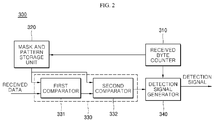
- Fig. 2 is a block diagram illustrating configuration of an Ethernet detecting circuit according to an embodiment of the present invention.
- the Ethernet detecting circuit 300 includes a received byte counter 310, a mask and pattern storage unit 320, a comparator 330, and a detection signal generator 340.
- the received byte counter 310 may count the byte of the Ethernet frame of received data. Thereby, the received byte counter 310 may calculate the byte count value of data which is being received. The received byte counter 310 may also transmit the calculated count value to the mask and pattern storage unit 320 and the detection signal generator 340.
- the mask and pattern storage unit 320 may calculate mask data and comparison data corresponding to the calculated count value based on the stored mask register and pattern register.
- the mask register may be a register having a length of L bytes and indicating a bit mask. Accordingly, the mask register may represent a register which is used to ignore bits which need not be detected.
- the mask data may represent a mask register corresponding to the calculated count value.
- the pattern register may be a register having a length of L bytes and indicating a bit comparison pattern. Accordingly, the pattern register may represent a register for indicating a pattern of frames to be detected.
- the comparison data may represent a pattern register corresponding to the calculated count value.
- the comparator 330 may compare the calculated mask data and comparison data with received data. For example, the comparator 330 may ignore bits which need not be detected in the received data, based on the calculated mask data. The comparator 330 may also detect a pattern of frames to be detected in the received data, based on the calculated comparison data. Herein, the data containing the pattern of frames to be detected may be referred to as target data. The comparator 330 transmits the result of comparison to the detection signal generator 340.
- the comparator 330 may include a plurality of comparators.
- the comparator 330 may include a first comparator 331 and a second comparator 332.
- the first comparator 331 may ignore bits which need not be detected in the received data, based on the calculated mask data.
- the second comparator 332 may compare the received data with the target data to be detected, based on the calculated comparison data.
- the received data may be sequentially transferred to the first comparator 331 and the second comparator 332.
- the detection signal generator 340 outputs a detection signal based on the result of comparison.
- the detection signal generator 340 may output a detection signal which indicates whether or not a frame having the maximum length of L bytes has been detected as a frame to be detected.
- the detection signal generator 340 may output 1. When the detected frame is not a frame to be detected, the detection signal generator 340 may output 0.
- Ethernet detecting circuit 300 operation of the Ethernet detecting circuit 300 will be described based on the above description.
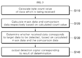
- Fig. 3 is a flowchart illustrating operation of an Ethernet detecting circuit according to an embodiment of the present invention.
- the received byte counter 310 of the Ethernet detecting circuit 300 calculates the byte count value of the data which is being received (S110).
- the received byte counter 310 may count the byte of data which is being received or has been received in the Ethernet frame. Thereby, the received byte counter 310 may calculate the byte count value of the data which is being received. The received byte counter 310 may transmit the calculated count value to the mask and pattern storage unit 320 and the detection signal generator 340.
- the mask and pattern storage unit 320 of the Ethernet detecting circuit 300 calculates the mask data and comparison data respectively based on the calculated count value (S120).
- the mask and pattern storage unit 320 may calculate mask data and comparison data corresponding to the calculated count value based on the stored mask register and pattern register.
- Fig. 4 is a block diagram of an Ethernet detecting circuit illustrating configuration of a mask and pattern storage unit according to an embodiment of the present invention.
- the mask and pattern storage unit 320 of the Ethernet detecting circuit 300 may include a mask register column 321, a first multiplexer (mux) 322, a pattern register column 323, and a second mux 324.
- the mask register column 321 may store a mask register.
- the first mux 322 may calculate mask data based on the mask register stored in the mask register column 321 and the calculated count value.
- the first mux 322 may select mask data from the mask register stored in the mask register column 321, taking the calculated count value as a selection signal.
- the first mux 322 may transmit the at calculated comparison mask data to the comparator 330.
- the first mux 322 may transmit the calculated mask data to the first comparator 331.
- the pattern register column 323 may store a pattern register.
- the second mux 324 may calculate comparison data based on the pattern register stored in the pattern register column 323 and the calculated count value.
- the second mux 324 may select comparison data from the pattern register stored in the pattern register column 323, taking the calculated count value as a selection signal.
- the second mux 324 may transmit the calculated comparison data to the comparator 330.
- the second mux 324 may transmit the calculated comparison data to the second comparator 332.
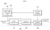
- Fig. 5 is a block diagram of an Ethernet detecting circuit illustrating configuration of a mask and pattern storage unit according to another embodiment of the present invention.
- the mask and pattern storage unit 320 of the Ethernet detecting circuit 300 include a mask and pattern storage memory 327.
- the mask and pattern storage memory 327 may store a mask register and pattern register.
- the mask and pattern storage memory 327 may calculate mask data and comparison data corresponding to the calculated count value, based on the stored mask register and pattern register.
- the mask and pattern storage memory 327 may transmit the calculated mask data and comparison data to the comparator 330.
- the mask and pattern storage memory 327 may transmit the calculated mask data to the first comparator 331, and transmit the calculate comparison data to the second comparator 332.
- the mask and pattern storage memory 327 may include various types of memories.
- the mask and pattern storage memory 327 may include at least one of a random access memory (RAM), a read-only memory (ROM) and a flash memory.
- the Ethernet detecting circuit 300 including the mask and pattern storage memory 327 can reduce the use of a device such as D-flip-flop. Accordingly, production costs of Ethernet detecting circuits may be reduced, and semiconductor chips constituting the Ethernet detecting circuit may be downsized.
- the comparator 330 of the Ethernet detecting circuit 300 determines whether the received data corresponds to data to be detected, based on the calculated mask data and comparison data (S130).
- the comparator 330 may compare the calculated comparison data with the received data.
- the comparator 330 may ignore bits which need not be detected in the received data, based on the calculated mask data.
- the comparator 330 may also detect a pattern of a frame to be detected in the received data, based on the calculated comparison data.
- data containing the pattern of frames to be detected may be referred to as target data.
- the comparator 330 may determine whether the received data corresponds to target data to be detected.
- the comparator 330 may transmit, to the detection signal generator 340, the result of determination according to comparison between the mask data and comparison data with the received data.
- the comparator 330 may include a plurality of the comparators.
- the comparator 330 may include a first comparator 331 and a second comparator 332.
- the first comparator 331 may ignore bits which need not be detected in the received data, based on the calculated mask data, and the second comparator 332 may compare the received data with the target data to be detected, based on the calculated comparison data.
- the first comparator 331 and the second comparator 332 may transmit the result of comparison to the detection signal generator 340.
- the detection signal generator 340 of the Ethernet detecting circuit 300 outputs a detection signal corresponding to the determination result (S140).
- the detection signal generator 340 outputs a detection signal based on the delivered determination result.
- the detection signal generator 340 may output a detection signal which indicates whether or not a frame having the maximum length of L bytes has been detected as a frame to be detected.
- the detection signal generator 340 may output 1. When the detected frame is not a frame to be detected, the detection signal generator 340 may output 0.
- the Ethernet detecting circuit 300 may output a detection signal indicating whether or not a frame having the maximum length of L bytes has been detected as a frame to be detected in the received data.
- the Ethernet detecting apparatus 400 may detect a plurality of frames simultaneously through a plurality of Ethernet detecting circuits 300.
- the Ethernet detecting apparatus 400 may detect Ethernet frames that having the size of N*L bytes simultaneously.
- the method described above can be implemented with processor-readable codes in a process-readable medium having a recorded program.
- the processor-readable medium may include one of ROM, RAM, CD-ROM, magnetic tapes, floppy discs, and optical data storage devices, and also include a carrier-wave type implementation (e.g., transmission via the Internet).
- Ethernet frames can be detected through various configurations, and thus property requirements for the Ethernet frame detecting apparatus may be satisfied.
- Ethernet frame detecting circuits may be reduced and configuration thereof may be simplified.
Landscapes
- Engineering & Computer Science (AREA)
- Computer Networks & Wireless Communication (AREA)
- Signal Processing (AREA)
- Health & Medical Sciences (AREA)
- Cardiology (AREA)
- General Health & Medical Sciences (AREA)
- Computer Security & Cryptography (AREA)
- Environmental & Geological Engineering (AREA)
- Small-Scale Networks (AREA)
- Communication Control (AREA)
Abstract
Description
- The present invention relates to an apparatus and method for detecting Ethernet frames and, more particularly, to an apparatus for detecting Ethernet frames in the field of Ethernet network communication.
- Ethernet is the most typical short-range communication network of a bus structure. To transmit data over the Ethernet, a Carrier Sense Multiple Access with Collision Detection (CSMA/CD) scheme is used.
- In transmitting data through an Ethernet frame, an Ethernet header and trailer are added to a data packet generated in the Internet layer, which is a higher layer, and then transmitted via a medium. When the data is received through the Ethernet frame, the header and the trailer are separated from each other, and the data packet is sent to the network layer.
- The Ethernet frame includes a Preamble field for announcing, to a receiver, transmission of the Ethernet frame and providing a synchronization signal enabling distinction between 0 and 1 in the frame to receive, a Start Delimiter field indicating the start position of the frame, a Destination MAC Address field, a Source MAC Address, a Length field indicating the size of transmitted data with a variable length contained in a data field, a data field, and a Checksum field enabling a receiver host to recognize occurrence of an error of data variation in the process of data transmission.
- To process Ethernet data, the received Ethernet frame needs to be detected and transferred through a path where the received Ethernet frame can be appropriately processed according to the result of the detection.
- According, there is a need for an Ethernet frame detecting apparatus capable of efficiently detecting Ethernet frames.
- It is an aspect of the present invention to efficiently detect Ethernet frames in various ways.
- It is another aspect of the present invention to reduce production costs of Ethernet frame detecting circuits and simplify configuration thereof.
- In accordance with one aspect of the present invention, an Ethernet frame detecting circuit for detecting Ethernet frames includes a received byte counter configured to calculate a byte count value of received data; a mask and pattern storage unit configured to calculate mask data and comparison data containing a pattern of a frame, based on the calculated byte count value; a comparator configured to determine whether the received data corresponds to target data to be detected, based on the calculated mask data and comparison data; and a detection signal generator configured to output a detection signal corresponding to a result of the determination.
- The mask and pattern storage unit may include a mask and pattern storage memory configured to store a mask register for ignoring bits which need not be detected and a pattern register indicating a frame to be detected and to calculate the mask data and comparison data corresponding to the calculated byte count value, based on the stored mask register and pattern register.
- The mask and pattern storage memory may include at least one of a random access memory (RAM), a read only memory (ROM) and a flash memory.
- The mask and pattern storage unit may include a mask register column configured to store a mask register for ignoring bits which need not be detected; a first multiplexer (mux) configured to calculate the mask data based on the mask register and the calculated byte count value; a pattern register column configured to store a pattern register indicating a frame to be detected; and a second mux configured to calculate the comparison data based on the pattern register and the calculated byte count value.
- The comparator may include a first comparator configured to ignore bits which need not be detected in the received data, based on the calculated mask data; and a second comparator configured to compare the received data with the target data to be detected, based on the calculated comparison data.
- With an apparatus and method for detecting Ethernet frames according to an embodiment of the present invention, Ethernet frames may be detected through various configurations and property requirements for the Ethernet frame detecting apparatus may be satisfied.
- In addition, production costs of the Ethernet frame detecting circuits may be reduced, and configuration may be simplified.
-
-
Fig. 1 is a block diagram illustrating configuration of an Ethernet system according to an embodiment of the present invention. -
Fig. 2 is a block diagram illustrating configuration of an Ethernet detecting circuit according to an embodiment of the present invention. -
Fig. 3 is a flowchart illustrating operation of an Ethernet detecting circuit according to an embodiment of the present invention. -
Fig. 4 is a block diagram of an Ethernet detecting circuit illustrating configuration of a mask and pattern storage unit according to an embodiment of the present invention. -
Fig. 5 is a block diagram of an Ethernet detecting circuit illustrating configuration of a mask and pattern storage unit according to another embodiment of the present invention. - Hereinafter, embodiments of the present invention will be described in detail with reference to the accompanying drawings. As used herein, the suffixes "module" and "unit" are added or used interchangeably to facilitate preparation of this specification and are not intended to suggest meanings or functions distinguished therebetween.
- Advantages and features of the present invention and methods to achieve them will become apparent from the descriptions of exemplary embodiments herein below with reference to the accompanying drawings. However, the present invention is not limited to exemplary embodiments disclosed herein but may be implemented in various different forms. The exemplary embodiments are provided for making the disclosure of the present invention thorough and for fully conveying the scope of the present invention to those skilled in the art. It is to be noted that the scope of the present invention is defined only by the claims. Like reference numerals denote like elements throughout the descriptions.
- In describing embodiments of the present invention disclosed in this specification, relevant well-known functions and constituents may not be described in detail if it is determined that such description can unnecessarily obscure the subject matter of the present invention. Terms which will be used below are defined in consideration of the functions of the corresponding elements in the embodiments of the present invention.
- It should be understood that the present invention is not limited to the following embodiments, and that the embodiments are provided for illustrative purposes only. The scope of the invention should be defined only by the accompanying claims and equivalents thereof. The definitions of the terms may vary depending on intention of a user or operator, a precedent case, or the like. Therefore, the terms should be defined based on the entire specification.
- It will be understood that each block of the flowchart illustrations and/or block diagrams, and combinations of blocks in the flowchart illustrations and/or block diagrams, can be implemented by computer program instructions. These computer program instructions may be provided to a processor of a general purpose computer, special purpose computer, or other programmable data processing apparatus to produce a machine, such that the instructions, which execute via the processor of the computer or other programmable data processing apparatus, create means for implementing the functions specified in the flowchart and/or block diagram block or blocks. These computer program instructions may also be stored in a computer-useable or computer-readable memory that can direct a computer or other programmable data processing apparatuses to function in a particular manner, such that the instructions stored in the computer-useable or computer-readable memory produce an article of manufacture including instructions which implement the function specified in the flowchart and/or block diagram block or blocks. The computer program instructions may also be loaded onto a computer or other programmable data processing apparatuses to cause a series of operational steps to be performed on the computer, other programmable apparatuses to produce a computer implemented process such that the instructions which execute on the computer or other programmable apparatuses provide processes for implementing the functions specified in the flowchart and/or block diagram block or blocks.
- In addition, each block or step in the flowchart or block diagrams may represent a module, segment, or portion of code, which comprises one or more executable instructions for implementing the specified logical function(s). It should also be noted that, in some alternative implementations, the functions noted in the blocks or steps may occur out of the order noted in the figures. For example, two blocks or steps shown in succession may, in fact, be executed substantially concurrently, or the blocks or steps may sometimes be executed in the reverse order, depending upon the functionality involved.
- Hereinafter, an
Ethernet system 10 according to an embodiment of the present invention will be described with reference toFig. 1 . -
FIG. 1 is a block diagram illustrating configuration of an Ethernet system according to an embodiment of the present invention. - Referring to
Fig. 1 , anEthernet system 10 includes an Ethernetnetwork 100, aphysical interface unit 200, and an Ethernet detectingapparatus 400. - The Ethernet
network 100 may represent a physical communication network. For example, the Ethernetnetwork 100 may represent a local area network (LAN) of a bus structure. - The
physical interface unit 200 may be an interface connected to the Ethernetnetwork 100 to receive data. The Ethernet detectingapparatus 400 may detect an Ethernet frame of received data. - The Ethernet detecting
apparatus 400 may include a plurality of Ethernet detectingcircuits - Herein, each Ethernet detecting circuit may detect one frame having the maximum length of L bytes. Thereby, the Ethernet detecting
apparatus 400 may detect n frames through a plurality of Ethernet detectingcircuits - For ease of description, a reference numeral '300' will be assigned to the Ethernet detecting circuits.
- Hereinafter, an Ethernet detecting
circuit 300 will be described in detail with reference toFig. 2 . -
Fig. 2 is a block diagram illustrating configuration of an Ethernet detecting circuit according to an embodiment of the present invention. - Referring to
Fig. 2 , the Ethernet detectingcircuit 300 includes a receivedbyte counter 310, a mask andpattern storage unit 320, acomparator 330, and adetection signal generator 340. - The received
byte counter 310 may count the byte of the Ethernet frame of received data. Thereby, the receivedbyte counter 310 may calculate the byte count value of data which is being received. The receivedbyte counter 310 may also transmit the calculated count value to the mask andpattern storage unit 320 and thedetection signal generator 340. - The mask and
pattern storage unit 320 may calculate mask data and comparison data corresponding to the calculated count value based on the stored mask register and pattern register. - Herein, the mask register may be a register having a length of L bytes and indicating a bit mask. Accordingly, the mask register may represent a register which is used to ignore bits which need not be detected. The mask data may represent a mask register corresponding to the calculated count value.
- The pattern register may be a register having a length of L bytes and indicating a bit comparison pattern. Accordingly, the pattern register may represent a register for indicating a pattern of frames to be detected. The comparison data may represent a pattern register corresponding to the calculated count value.
- The
comparator 330 may compare the calculated mask data and comparison data with received data. For example, thecomparator 330 may ignore bits which need not be detected in the received data, based on the calculated mask data. Thecomparator 330 may also detect a pattern of frames to be detected in the received data, based on the calculated comparison data. Herein, the data containing the pattern of frames to be detected may be referred to as target data. Thecomparator 330 transmits the result of comparison to thedetection signal generator 340. - Meanwhile, the
comparator 330 may include a plurality of comparators. For example, thecomparator 330 may include afirst comparator 331 and asecond comparator 332. - The
first comparator 331 may ignore bits which need not be detected in the received data, based on the calculated mask data. - The
second comparator 332 may compare the received data with the target data to be detected, based on the calculated comparison data. - The received data may be sequentially transferred to the
first comparator 331 and thesecond comparator 332. - The
detection signal generator 340 outputs a detection signal based on the result of comparison. - The
detection signal generator 340 may output a detection signal which indicates whether or not a frame having the maximum length of L bytes has been detected as a frame to be detected. - For example, when a frame to be detected is detected, the
detection signal generator 340may output 1. When the detected frame is not a frame to be detected, thedetection signal generator 340 may output 0. - Hereinafter, operation of the
Ethernet detecting circuit 300 will be described based on the above description. -
Fig. 3 is a flowchart illustrating operation of an Ethernet detecting circuit according to an embodiment of the present invention. - Referring to
Fig. 3 , the receivedbyte counter 310 of theEthernet detecting circuit 300 calculates the byte count value of the data which is being received (S110). - The received
byte counter 310 may count the byte of data which is being received or has been received in the Ethernet frame. Thereby, the receivedbyte counter 310 may calculate the byte count value of the data which is being received. The receivedbyte counter 310 may transmit the calculated count value to the mask andpattern storage unit 320 and thedetection signal generator 340. - The mask and
pattern storage unit 320 of theEthernet detecting circuit 300 calculates the mask data and comparison data respectively based on the calculated count value (S120). - The mask and
pattern storage unit 320 may calculate mask data and comparison data corresponding to the calculated count value based on the stored mask register and pattern register. - An example will be described with reference to
Fig. 4 . -
Fig. 4 is a block diagram of an Ethernet detecting circuit illustrating configuration of a mask and pattern storage unit according to an embodiment of the present invention. - Referring to
Fig. 4 , the mask andpattern storage unit 320 of theEthernet detecting circuit 300 may include amask register column 321, a first multiplexer (mux) 322, apattern register column 323, and asecond mux 324. - The
mask register column 321 may store a mask register. - The
first mux 322 may calculate mask data based on the mask register stored in themask register column 321 and the calculated count value. - For example, the
first mux 322 may select mask data from the mask register stored in themask register column 321, taking the calculated count value as a selection signal. - The
first mux 322 may transmit the at calculated comparison mask data to thecomparator 330. For example, thefirst mux 322 may transmit the calculated mask data to thefirst comparator 331. - The
pattern register column 323 may store a pattern register. - The
second mux 324 may calculate comparison data based on the pattern register stored in thepattern register column 323 and the calculated count value. - For example, the
second mux 324 may select comparison data from the pattern register stored in thepattern register column 323, taking the calculated count value as a selection signal. - The
second mux 324 may transmit the calculated comparison data to thecomparator 330. For example, thesecond mux 324 may transmit the calculated comparison data to thesecond comparator 332. - Hereinafter, another embodiment will be described with reference to
Fig. 5 . -
Fig. 5 is a block diagram of an Ethernet detecting circuit illustrating configuration of a mask and pattern storage unit according to another embodiment of the present invention. - Referring to
Fig. 5 , the mask andpattern storage unit 320 of theEthernet detecting circuit 300 include a mask andpattern storage memory 327. - The mask and
pattern storage memory 327 may store a mask register and pattern register. The mask andpattern storage memory 327 may calculate mask data and comparison data corresponding to the calculated count value, based on the stored mask register and pattern register. The mask andpattern storage memory 327 may transmit the calculated mask data and comparison data to thecomparator 330. For example, the mask andpattern storage memory 327 may transmit the calculated mask data to thefirst comparator 331, and transmit the calculate comparison data to thesecond comparator 332. - The mask and
pattern storage memory 327 may include various types of memories. For example, the mask andpattern storage memory 327 may include at least one of a random access memory (RAM), a read-only memory (ROM) and a flash memory. - The
Ethernet detecting circuit 300 including the mask andpattern storage memory 327 can reduce the use of a device such as D-flip-flop. Accordingly, production costs of Ethernet detecting circuits may be reduced, and semiconductor chips constituting the Ethernet detecting circuit may be downsized. - Description will be given with reference back to
Fig. 3 . - The
comparator 330 of theEthernet detecting circuit 300 determines whether the received data corresponds to data to be detected, based on the calculated mask data and comparison data (S130). - The
comparator 330 may compare the calculated comparison data with the received data. - For example, the
comparator 330 may ignore bits which need not be detected in the received data, based on the calculated mask data. Thecomparator 330 may also detect a pattern of a frame to be detected in the received data, based on the calculated comparison data. Herein, data containing the pattern of frames to be detected may be referred to as target data. Thus, thecomparator 330 may determine whether the received data corresponds to target data to be detected. Thecomparator 330 may transmit, to thedetection signal generator 340, the result of determination according to comparison between the mask data and comparison data with the received data. - As described above, the
comparator 330 may include a plurality of the comparators. - For example, the
comparator 330 may include afirst comparator 331 and asecond comparator 332. - The
first comparator 331 may ignore bits which need not be detected in the received data, based on the calculated mask data, and thesecond comparator 332 may compare the received data with the target data to be detected, based on the calculated comparison data. Thefirst comparator 331 and thesecond comparator 332 may transmit the result of comparison to thedetection signal generator 340. - The
detection signal generator 340 of theEthernet detecting circuit 300 outputs a detection signal corresponding to the determination result (S140). - The
detection signal generator 340 outputs a detection signal based on the delivered determination result. - The
detection signal generator 340 may output a detection signal which indicates whether or not a frame having the maximum length of L bytes has been detected as a frame to be detected. - For example, when a frame to be detected is detected, the
detection signal generator 340may output 1. When the detected frame is not a frame to be detected, thedetection signal generator 340 may output 0. - As described above, the
Ethernet detecting circuit 300 may output a detection signal indicating whether or not a frame having the maximum length of L bytes has been detected as a frame to be detected in the received data. - The
Ethernet detecting apparatus 400 may detect a plurality of frames simultaneously through a plurality ofEthernet detecting circuits 300. - Thereby, when the
Ethernet detecting apparatus 400 includes nEthernet detecting circuit 300, theEthernet detecting apparatus 400 may detect Ethernet frames that having the size of N*L bytes simultaneously. - According to an embodiment of the present invention, the method described above can be implemented with processor-readable codes in a process-readable medium having a recorded program. Examples of the processor-readable medium may include one of ROM, RAM, CD-ROM, magnetic tapes, floppy discs, and optical data storage devices, and also include a carrier-wave type implementation (e.g., transmission via the Internet).
- With an apparatus and method for detecting Ethernet frames according to embodiments of the present invention, Ethernet frames can be detected through various configurations, and thus property requirements for the Ethernet frame detecting apparatus may be satisfied.
- According embodiments of the present invention, production costs of Ethernet frame detecting circuits may be reduced and configuration thereof may be simplified.
- The configuration and method described above are not limited to the embodiments disclosed in the foregoing description. A part or entirety of the embodiments may be selectively combined to enable various modifications.
- While preferred embodiments of the present invention have been described above, it should be understood that they have been presented by way of example only, and not limitation. It will be apparent to persons skilled in the art that various modifications and variations can be made to the present invention without departing from the spirit and scope of the invention as disclosed in the accompanying claims. Thus, it is intended that the present invention include modifications and variations that are within the scope of the appended claims and their equivalents.
Claims (5)
- An Ethernet frame detecting circuit (300) for detecting Ethernet frames, comprising:a received byte counter (310) configured to calculate a byte count value of received data;a mask and pattern storage unit (320) configured to calculate mask data and comparison data containing a pattern of a frame, based on the calculated byte count value;a comparator (330) configured to determine whether the received data corresponds to target data to be detected, based on the calculated mask data and comparison data; anda detection signal generator (340) configured to output a detection signal corresponding to a result of the determination.
- The Ethernet frame detecting circuit according to claim 1, wherein the mask and pattern storage unit (320) comprises:a mask and pattern storage memory (327) configured to store a mask register for ignoring bits which need not be detected and a pattern register indicating a frame to be detected and to calculate the mask data and comparison data corresponding to the calculated byte count value, based on the stored mask register and pattern register.
- The Ethernet frame detecting circuit according to claim 2, wherein the mask and pattern storage memory (327) comprises at least one of a random access memory, RAM, a read only memory, ROM, and a flash memory.
- The Ethernet frame detecting circuit according to claim 1, wherein the mask and pattern storage unit (320) comprises:a mask register column (321) configured to store a mask register for ignoring bits which need not be detected;a first multiplexer, mux, (322) configured to calculate the mask data based on the mask register and the calculated byte count value;a pattern register column (323) configured to store a pattern register indicating a frame to be detected; anda second mux (324) configured to calculate the comparison data based on the pattern register and the calculated byte count value.
- The Ethernet frame detecting circuit according to claim 1, wherein the comparator (330) comprises:a first comparator (331) configured to ignore bits which need not be detected in the received data, based on the calculated mask data; anda second comparator (332) configured to compare the received data with the target data to be detected, based on the calculated comparison data.
Applications Claiming Priority (1)
| Application Number | Priority Date | Filing Date | Title |
|---|---|---|---|
| KR1020150108399A KR101649828B1 (en) | 2015-07-30 | 2015-07-30 | Apparatus and method for detectioning of ethenet frame |
Publications (2)
| Publication Number | Publication Date |
|---|---|
| EP3125470A1 true EP3125470A1 (en) | 2017-02-01 |
| EP3125470B1 EP3125470B1 (en) | 2019-05-15 |
Family
ID=56617984
Family Applications (1)
| Application Number | Title | Priority Date | Filing Date |
|---|---|---|---|
| EP16176638.1A Active EP3125470B1 (en) | 2015-07-30 | 2016-06-28 | Apparatus for detecting ethernet frame |
Country Status (6)
| Country | Link |
|---|---|
| US (1) | US10063390B2 (en) |
| EP (1) | EP3125470B1 (en) |
| JP (2) | JP2017034673A (en) |
| KR (1) | KR101649828B1 (en) |
| CN (1) | CN106411564B (en) |
| ES (1) | ES2735739T3 (en) |
Families Citing this family (3)
| Publication number | Priority date | Publication date | Assignee | Title |
|---|---|---|---|---|
| CN112332951B (en) * | 2020-11-20 | 2022-06-24 | 昆高新芯微电子(江苏)有限公司 | Ethernet frame preemption method, device, equipment and storage medium |
| CN112737995B (en) * | 2020-12-16 | 2022-11-22 | 北京东土科技股份有限公司 | Processing method, device, equipment and storage medium of Ethernet frame |
| EP4113951B1 (en) * | 2021-06-29 | 2025-01-01 | Renesas Electronics Corporation | Frame data processing |
Citations (3)
| Publication number | Priority date | Publication date | Assignee | Title |
|---|---|---|---|---|
| US20020077995A1 (en) * | 1998-04-28 | 2002-06-20 | Samuel Steven Allison | Pattern matching in communications network |
| US20040190506A1 (en) * | 2003-03-24 | 2004-09-30 | International Business Machines Corp. | Method and apparatus for performing complex pattern matching in a data stream within a computer network |
| US7373454B1 (en) * | 2003-10-28 | 2008-05-13 | Altera Corporation | Pattern detect and byte align circuit using CAM |
Family Cites Families (13)
| Publication number | Priority date | Publication date | Assignee | Title |
|---|---|---|---|---|
| US5935245A (en) * | 1996-12-13 | 1999-08-10 | 3Com Corporation | Method and apparatus for providing secure network communications |
| TW498206B (en) * | 1998-07-28 | 2002-08-11 | Silicon Integrated Sys Corp | Method and device for matching data stream with a fixed pattern |
| JP2001189752A (en) * | 1999-12-28 | 2001-07-10 | Sony Corp | Packet selection apparatus and method and reception apparatus |
| US7230956B1 (en) * | 2003-01-10 | 2007-06-12 | Altera Corporation | Techniques for frame detection and word alignment |
| JP4341413B2 (en) * | 2003-07-11 | 2009-10-07 | 株式会社日立製作所 | PACKET TRANSFER APPARATUS HAVING STATISTICS COLLECTION APPARATUS AND STATISTICS COLLECTION METHOD |
| KR20050019952A (en) | 2003-08-18 | 2005-03-04 | 엘지전자 주식회사 | Frame detecting apparatus and method in communication system using digital signal 3 |
| US7921263B2 (en) * | 2006-12-22 | 2011-04-05 | Broadcom Corporation | System and method for performing masked store operations in a processor |
| JP2010161676A (en) * | 2009-01-09 | 2010-07-22 | Panasonic Corp | Microcomputer with radio communication function and application system therefor |
| KR101276261B1 (en) | 2011-09-21 | 2013-06-20 | 주식회사 마스터소프트 | Security System For Remote Connection |
| KR101414959B1 (en) | 2012-02-29 | 2014-07-09 | 주식회사 팬택 | A detecting method of a network attack and a mobile terminal detecting a network attack |
| US8997231B2 (en) | 2012-04-18 | 2015-03-31 | Zimperium, Inc. | Preventive intrusion device and method for mobile devices |
| KR101558054B1 (en) | 2012-11-19 | 2015-10-06 | 삼성에스디에스 주식회사 | Anti-malware system and packet processing method in same |
| KR20140077489A (en) | 2012-12-14 | 2014-06-24 | 삼성전자주식회사 | user terminal apparatus, network apparatus and control method thereof |
-
2015
- 2015-07-30 KR KR1020150108399A patent/KR101649828B1/en active Active
-
2016
- 2016-06-28 EP EP16176638.1A patent/EP3125470B1/en active Active
- 2016-06-28 ES ES16176638T patent/ES2735739T3/en active Active
- 2016-07-25 CN CN201610592947.5A patent/CN106411564B/en active Active
- 2016-07-28 JP JP2016148193A patent/JP2017034673A/en active Pending
- 2016-07-29 US US15/224,360 patent/US10063390B2/en active Active
-
2018
- 2018-10-19 JP JP2018197731A patent/JP6567754B2/en not_active Expired - Fee Related
Patent Citations (3)
| Publication number | Priority date | Publication date | Assignee | Title |
|---|---|---|---|---|
| US20020077995A1 (en) * | 1998-04-28 | 2002-06-20 | Samuel Steven Allison | Pattern matching in communications network |
| US20040190506A1 (en) * | 2003-03-24 | 2004-09-30 | International Business Machines Corp. | Method and apparatus for performing complex pattern matching in a data stream within a computer network |
| US7373454B1 (en) * | 2003-10-28 | 2008-05-13 | Altera Corporation | Pattern detect and byte align circuit using CAM |
Also Published As
| Publication number | Publication date |
|---|---|
| US10063390B2 (en) | 2018-08-28 |
| ES2735739T3 (en) | 2019-12-20 |
| JP6567754B2 (en) | 2019-08-28 |
| JP2019030025A (en) | 2019-02-21 |
| CN106411564B (en) | 2019-09-06 |
| US20170033945A1 (en) | 2017-02-02 |
| JP2017034673A (en) | 2017-02-09 |
| KR101649828B1 (en) | 2016-08-19 |
| CN106411564A (en) | 2017-02-15 |
| EP3125470B1 (en) | 2019-05-15 |
Similar Documents
| Publication | Publication Date | Title |
|---|---|---|
| JP5770924B2 (en) | Method and apparatus for increasing data transmission capacity in a serial bus system | |
| US10491418B2 (en) | Can controller and data transmission method using the same | |
| EP3361677A1 (en) | Communication device, communication method and communication program | |
| US12083971B2 (en) | Anomaly handling method and anomaly handling device | |
| US9531750B2 (en) | Spoofing detection | |
| US10542095B2 (en) | Synchronization measurement system, synchronization measurement method, controller, sensor unit, synchronous signal generation unit, synchronous signal transfer unit, and program | |
| EP3125470B1 (en) | Apparatus for detecting ethernet frame | |
| CN104702468A (en) | Transmission path determining method, device and system | |
| US20170272339A1 (en) | Method and apparatus for detecting connectivity | |
| US10318453B2 (en) | Systems and methods for transmitting interrupts between nodes | |
| US10880119B2 (en) | Method for removing data frame redundancy in network environment, and device and computer program for carrying out same | |
| KR102204954B1 (en) | Can controller and method for transmission of data using the same | |
| CN106452894A (en) | Fault connection detection method and apparatus | |
| KR101714770B1 (en) | ID Dynamic Allocating Method for CAN Communication System, and CAN Communication System | |
| JP5902844B2 (en) | Method and apparatus for serial data transmission with flexible message size and variable bit length | |
| JP5815085B1 (en) | Communication system, communication apparatus, connection state determination method, and control program | |
| CN106664636B (en) | Data frame transmission method and device | |
| US12506554B2 (en) | Time synchronization method, device and apparatus, and storage medium | |
| EP3068079B1 (en) | Monitoring communication in a network comprising a plurality of nodes | |
| CN109150646B (en) | Link state detection system, method and apparatus | |
| CN106506309B (en) | communication interface device | |
| CN105591830B (en) | A kind of detection method and device for link modification | |
| US10476776B2 (en) | Methods, systems and computer readable media for wide bus pattern matching | |
| WO2015054830A1 (en) | Method and device for processing radio access network information management information |
Legal Events
| Date | Code | Title | Description |
|---|---|---|---|
| PUAI | Public reference made under article 153(3) epc to a published international application that has entered the european phase |
Free format text: ORIGINAL CODE: 0009012 |
|
| STAA | Information on the status of an ep patent application or granted ep patent |
Free format text: STATUS: THE APPLICATION HAS BEEN PUBLISHED |
|
| AK | Designated contracting states |
Kind code of ref document: A1 Designated state(s): AL AT BE BG CH CY CZ DE DK EE ES FI FR GB GR HR HU IE IS IT LI LT LU LV MC MK MT NL NO PL PT RO RS SE SI SK SM TR |
|
| AX | Request for extension of the european patent |
Extension state: BA ME |
|
| STAA | Information on the status of an ep patent application or granted ep patent |
Free format text: STATUS: REQUEST FOR EXAMINATION WAS MADE |
|
| 17P | Request for examination filed |
Effective date: 20170727 |
|
| RBV | Designated contracting states (corrected) |
Designated state(s): AL AT BE BG CH CY CZ DE DK EE ES FI FR GB GR HR HU IE IS IT LI LT LU LV MC MK MT NL NO PL PT RO RS SE SI SK SM TR |
|
| RIC1 | Information provided on ipc code assigned before grant |
Ipc: H04L 12/26 20060101AFI20181207BHEP |
|
| GRAP | Despatch of communication of intention to grant a patent |
Free format text: ORIGINAL CODE: EPIDOSNIGR1 |
|
| STAA | Information on the status of an ep patent application or granted ep patent |
Free format text: STATUS: GRANT OF PATENT IS INTENDED |
|
| INTG | Intention to grant announced |
Effective date: 20190207 |
|
| GRAS | Grant fee paid |
Free format text: ORIGINAL CODE: EPIDOSNIGR3 |
|
| GRAA | (expected) grant |
Free format text: ORIGINAL CODE: 0009210 |
|
| STAA | Information on the status of an ep patent application or granted ep patent |
Free format text: STATUS: THE PATENT HAS BEEN GRANTED |
|
| AK | Designated contracting states |
Kind code of ref document: B1 Designated state(s): AL AT BE BG CH CY CZ DE DK EE ES FI FR GB GR HR HU IE IS IT LI LT LU LV MC MK MT NL NO PL PT RO RS SE SI SK SM TR |
|
| REG | Reference to a national code |
Ref country code: CH Ref legal event code: EP |
|
| REG | Reference to a national code |
Ref country code: DE Ref legal event code: R096 Ref document number: 602016013884 Country of ref document: DE |
|
| REG | Reference to a national code |
Ref country code: IE Ref legal event code: FG4D |
|
| REG | Reference to a national code |
Ref country code: NL Ref legal event code: MP Effective date: 20190515 |
|
| REG | Reference to a national code |
Ref country code: LT Ref legal event code: MG4D |
|
| PG25 | Lapsed in a contracting state [announced via postgrant information from national office to epo] |
Ref country code: FI Free format text: LAPSE BECAUSE OF FAILURE TO SUBMIT A TRANSLATION OF THE DESCRIPTION OR TO PAY THE FEE WITHIN THE PRESCRIBED TIME-LIMIT Effective date: 20190515 Ref country code: LT Free format text: LAPSE BECAUSE OF FAILURE TO SUBMIT A TRANSLATION OF THE DESCRIPTION OR TO PAY THE FEE WITHIN THE PRESCRIBED TIME-LIMIT Effective date: 20190515 Ref country code: NL Free format text: LAPSE BECAUSE OF FAILURE TO SUBMIT A TRANSLATION OF THE DESCRIPTION OR TO PAY THE FEE WITHIN THE PRESCRIBED TIME-LIMIT Effective date: 20190515 Ref country code: HR Free format text: LAPSE BECAUSE OF FAILURE TO SUBMIT A TRANSLATION OF THE DESCRIPTION OR TO PAY THE FEE WITHIN THE PRESCRIBED TIME-LIMIT Effective date: 20190515 Ref country code: SE Free format text: LAPSE BECAUSE OF FAILURE TO SUBMIT A TRANSLATION OF THE DESCRIPTION OR TO PAY THE FEE WITHIN THE PRESCRIBED TIME-LIMIT Effective date: 20190515 Ref country code: AL Free format text: LAPSE BECAUSE OF FAILURE TO SUBMIT A TRANSLATION OF THE DESCRIPTION OR TO PAY THE FEE WITHIN THE PRESCRIBED TIME-LIMIT Effective date: 20190515 Ref country code: PT Free format text: LAPSE BECAUSE OF FAILURE TO SUBMIT A TRANSLATION OF THE DESCRIPTION OR TO PAY THE FEE WITHIN THE PRESCRIBED TIME-LIMIT Effective date: 20190915 Ref country code: NO Free format text: LAPSE BECAUSE OF FAILURE TO SUBMIT A TRANSLATION OF THE DESCRIPTION OR TO PAY THE FEE WITHIN THE PRESCRIBED TIME-LIMIT Effective date: 20190815 |
|
| PG25 | Lapsed in a contracting state [announced via postgrant information from national office to epo] |
Ref country code: GR Free format text: LAPSE BECAUSE OF FAILURE TO SUBMIT A TRANSLATION OF THE DESCRIPTION OR TO PAY THE FEE WITHIN THE PRESCRIBED TIME-LIMIT Effective date: 20190816 Ref country code: LV Free format text: LAPSE BECAUSE OF FAILURE TO SUBMIT A TRANSLATION OF THE DESCRIPTION OR TO PAY THE FEE WITHIN THE PRESCRIBED TIME-LIMIT Effective date: 20190515 Ref country code: RS Free format text: LAPSE BECAUSE OF FAILURE TO SUBMIT A TRANSLATION OF THE DESCRIPTION OR TO PAY THE FEE WITHIN THE PRESCRIBED TIME-LIMIT Effective date: 20190515 Ref country code: BG Free format text: LAPSE BECAUSE OF FAILURE TO SUBMIT A TRANSLATION OF THE DESCRIPTION OR TO PAY THE FEE WITHIN THE PRESCRIBED TIME-LIMIT Effective date: 20190815 |
|
| REG | Reference to a national code |
Ref country code: AT Ref legal event code: MK05 Ref document number: 1134701 Country of ref document: AT Kind code of ref document: T Effective date: 20190515 |
|
| REG | Reference to a national code |
Ref country code: ES Ref legal event code: FG2A Ref document number: 2735739 Country of ref document: ES Kind code of ref document: T3 Effective date: 20191220 |
|
| PG25 | Lapsed in a contracting state [announced via postgrant information from national office to epo] |
Ref country code: SK Free format text: LAPSE BECAUSE OF FAILURE TO SUBMIT A TRANSLATION OF THE DESCRIPTION OR TO PAY THE FEE WITHIN THE PRESCRIBED TIME-LIMIT Effective date: 20190515 Ref country code: CZ Free format text: LAPSE BECAUSE OF FAILURE TO SUBMIT A TRANSLATION OF THE DESCRIPTION OR TO PAY THE FEE WITHIN THE PRESCRIBED TIME-LIMIT Effective date: 20190515 Ref country code: DK Free format text: LAPSE BECAUSE OF FAILURE TO SUBMIT A TRANSLATION OF THE DESCRIPTION OR TO PAY THE FEE WITHIN THE PRESCRIBED TIME-LIMIT Effective date: 20190515 Ref country code: EE Free format text: LAPSE BECAUSE OF FAILURE TO SUBMIT A TRANSLATION OF THE DESCRIPTION OR TO PAY THE FEE WITHIN THE PRESCRIBED TIME-LIMIT Effective date: 20190515 Ref country code: AT Free format text: LAPSE BECAUSE OF FAILURE TO SUBMIT A TRANSLATION OF THE DESCRIPTION OR TO PAY THE FEE WITHIN THE PRESCRIBED TIME-LIMIT Effective date: 20190515 |
|
| REG | Reference to a national code |
Ref country code: CH Ref legal event code: PL |
|
| REG | Reference to a national code |
Ref country code: DE Ref legal event code: R097 Ref document number: 602016013884 Country of ref document: DE |
|
| PG25 | Lapsed in a contracting state [announced via postgrant information from national office to epo] |
Ref country code: SM Free format text: LAPSE BECAUSE OF FAILURE TO SUBMIT A TRANSLATION OF THE DESCRIPTION OR TO PAY THE FEE WITHIN THE PRESCRIBED TIME-LIMIT Effective date: 20190515 Ref country code: MC Free format text: LAPSE BECAUSE OF FAILURE TO SUBMIT A TRANSLATION OF THE DESCRIPTION OR TO PAY THE FEE WITHIN THE PRESCRIBED TIME-LIMIT Effective date: 20190515 |
|
| PLBE | No opposition filed within time limit |
Free format text: ORIGINAL CODE: 0009261 |
|
| STAA | Information on the status of an ep patent application or granted ep patent |
Free format text: STATUS: NO OPPOSITION FILED WITHIN TIME LIMIT |
|
| REG | Reference to a national code |
Ref country code: BE Ref legal event code: MM Effective date: 20190630 |
|
| PG25 | Lapsed in a contracting state [announced via postgrant information from national office to epo] |
Ref country code: TR Free format text: LAPSE BECAUSE OF FAILURE TO SUBMIT A TRANSLATION OF THE DESCRIPTION OR TO PAY THE FEE WITHIN THE PRESCRIBED TIME-LIMIT Effective date: 20190515 |
|
| 26N | No opposition filed |
Effective date: 20200218 |
|
| PG25 | Lapsed in a contracting state [announced via postgrant information from national office to epo] |
Ref country code: IE Free format text: LAPSE BECAUSE OF NON-PAYMENT OF DUE FEES Effective date: 20190628 Ref country code: PL Free format text: LAPSE BECAUSE OF FAILURE TO SUBMIT A TRANSLATION OF THE DESCRIPTION OR TO PAY THE FEE WITHIN THE PRESCRIBED TIME-LIMIT Effective date: 20190515 |
|
| PG25 | Lapsed in a contracting state [announced via postgrant information from national office to epo] |
Ref country code: SI Free format text: LAPSE BECAUSE OF FAILURE TO SUBMIT A TRANSLATION OF THE DESCRIPTION OR TO PAY THE FEE WITHIN THE PRESCRIBED TIME-LIMIT Effective date: 20190515 Ref country code: LI Free format text: LAPSE BECAUSE OF NON-PAYMENT OF DUE FEES Effective date: 20190630 Ref country code: CH Free format text: LAPSE BECAUSE OF NON-PAYMENT OF DUE FEES Effective date: 20190630 Ref country code: BE Free format text: LAPSE BECAUSE OF NON-PAYMENT OF DUE FEES Effective date: 20190630 Ref country code: LU Free format text: LAPSE BECAUSE OF NON-PAYMENT OF DUE FEES Effective date: 20190628 |
|
| PG25 | Lapsed in a contracting state [announced via postgrant information from national office to epo] |
Ref country code: RO Free format text: LAPSE BECAUSE OF FAILURE TO SUBMIT A TRANSLATION OF THE DESCRIPTION OR TO PAY THE FEE WITHIN THE PRESCRIBED TIME-LIMIT Effective date: 20190515 |
|
| PG25 | Lapsed in a contracting state [announced via postgrant information from national office to epo] |
Ref country code: CY Free format text: LAPSE BECAUSE OF FAILURE TO SUBMIT A TRANSLATION OF THE DESCRIPTION OR TO PAY THE FEE WITHIN THE PRESCRIBED TIME-LIMIT Effective date: 20190515 |
|
| PG25 | Lapsed in a contracting state [announced via postgrant information from national office to epo] |
Ref country code: IS Free format text: LAPSE BECAUSE OF FAILURE TO SUBMIT A TRANSLATION OF THE DESCRIPTION OR TO PAY THE FEE WITHIN THE PRESCRIBED TIME-LIMIT Effective date: 20190915 |
|
| PG25 | Lapsed in a contracting state [announced via postgrant information from national office to epo] |
Ref country code: HU Free format text: LAPSE BECAUSE OF FAILURE TO SUBMIT A TRANSLATION OF THE DESCRIPTION OR TO PAY THE FEE WITHIN THE PRESCRIBED TIME-LIMIT; INVALID AB INITIO Effective date: 20160628 Ref country code: MT Free format text: LAPSE BECAUSE OF FAILURE TO SUBMIT A TRANSLATION OF THE DESCRIPTION OR TO PAY THE FEE WITHIN THE PRESCRIBED TIME-LIMIT Effective date: 20190515 |
|
| REG | Reference to a national code |
Ref country code: DE Ref legal event code: R079 Ref document number: 602016013884 Country of ref document: DE Free format text: PREVIOUS MAIN CLASS: H04L0012260000 Ipc: H04L0043000000 |
|
| PG25 | Lapsed in a contracting state [announced via postgrant information from national office to epo] |
Ref country code: MK Free format text: LAPSE BECAUSE OF FAILURE TO SUBMIT A TRANSLATION OF THE DESCRIPTION OR TO PAY THE FEE WITHIN THE PRESCRIBED TIME-LIMIT Effective date: 20190515 |
|
| PGFP | Annual fee paid to national office [announced via postgrant information from national office to epo] |
Ref country code: GB Payment date: 20220405 Year of fee payment: 7 |
|
| PGFP | Annual fee paid to national office [announced via postgrant information from national office to epo] |
Ref country code: ES Payment date: 20220711 Year of fee payment: 7 |
|
| P01 | Opt-out of the competence of the unified patent court (upc) registered |
Effective date: 20230625 |
|
| GBPC | Gb: european patent ceased through non-payment of renewal fee |
Effective date: 20230628 |
|
| PG25 | Lapsed in a contracting state [announced via postgrant information from national office to epo] |
Ref country code: GB Free format text: LAPSE BECAUSE OF NON-PAYMENT OF DUE FEES Effective date: 20230628 |
|
| REG | Reference to a national code |
Ref country code: ES Ref legal event code: FD2A Effective date: 20240802 |
|
| PG25 | Lapsed in a contracting state [announced via postgrant information from national office to epo] |
Ref country code: ES Free format text: LAPSE BECAUSE OF NON-PAYMENT OF DUE FEES Effective date: 20230629 |
|
| PG25 | Lapsed in a contracting state [announced via postgrant information from national office to epo] |
Ref country code: ES Free format text: LAPSE BECAUSE OF NON-PAYMENT OF DUE FEES Effective date: 20230629 |
|
| PGFP | Annual fee paid to national office [announced via postgrant information from national office to epo] |
Ref country code: DE Payment date: 20250305 Year of fee payment: 10 |
|
| PGFP | Annual fee paid to national office [announced via postgrant information from national office to epo] |
Ref country code: IT Payment date: 20260306 Year of fee payment: 11 |
|
| PGFP | Annual fee paid to national office [announced via postgrant information from national office to epo] |
Ref country code: FR Payment date: 20260309 Year of fee payment: 11 |