EP3117463B1 - Igbt structure for wide band-gap semiconductor materials - Google Patents
Igbt structure for wide band-gap semiconductor materials Download PDFInfo
- Publication number
- EP3117463B1 EP3117463B1 EP15745260.8A EP15745260A EP3117463B1 EP 3117463 B1 EP3117463 B1 EP 3117463B1 EP 15745260 A EP15745260 A EP 15745260A EP 3117463 B1 EP3117463 B1 EP 3117463B1
- Authority
- EP
- European Patent Office
- Prior art keywords
- region
- igbt
- doping concentration
- stack
- spreading
- Prior art date
- Legal status (The legal status is an assumption and is not a legal conclusion. Google has not performed a legal analysis and makes no representation as to the accuracy of the status listed.)
- Active
Links
- 239000000463 material Substances 0.000 title claims description 11
- 239000004065 semiconductor Substances 0.000 title claims description 9
- 238000003892 spreading Methods 0.000 claims description 59
- 230000007480 spreading Effects 0.000 claims description 59
- 239000007943 implant Substances 0.000 claims description 49
- 238000000034 method Methods 0.000 claims description 38
- HBMJWWWQQXIZIP-UHFFFAOYSA-N silicon carbide Chemical group [Si+]#[C-] HBMJWWWQQXIZIP-UHFFFAOYSA-N 0.000 claims description 22
- 229910010271 silicon carbide Inorganic materials 0.000 claims description 20
- 229910003465 moissanite Inorganic materials 0.000 claims 2
- 230000008569 process Effects 0.000 description 25
- 239000000758 substrate Substances 0.000 description 12
- 238000005468 ion implantation Methods 0.000 description 8
- 238000004519 manufacturing process Methods 0.000 description 8
- 238000002347 injection Methods 0.000 description 7
- 239000007924 injection Substances 0.000 description 7
- 230000000903 blocking effect Effects 0.000 description 6
- 238000000407 epitaxy Methods 0.000 description 6
- 238000001465 metallisation Methods 0.000 description 5
- 230000008901 benefit Effects 0.000 description 3
- 230000003292 diminished effect Effects 0.000 description 3
- 239000002019 doping agent Substances 0.000 description 3
- 230000000694 effects Effects 0.000 description 3
- IJGRMHOSHXDMSA-UHFFFAOYSA-N Atomic nitrogen Chemical compound N#N IJGRMHOSHXDMSA-UHFFFAOYSA-N 0.000 description 2
- 239000000969 carrier Substances 0.000 description 2
- 230000007423 decrease Effects 0.000 description 2
- 230000003247 decreasing effect Effects 0.000 description 2
- 230000007547 defect Effects 0.000 description 2
- 230000005669 field effect Effects 0.000 description 2
- 238000012986 modification Methods 0.000 description 2
- 230000004048 modification Effects 0.000 description 2
- 230000003647 oxidation Effects 0.000 description 2
- 238000007254 oxidation reaction Methods 0.000 description 2
- ZOXJGFHDIHLPTG-UHFFFAOYSA-N Boron Chemical compound [B] ZOXJGFHDIHLPTG-UHFFFAOYSA-N 0.000 description 1
- XUIMIQQOPSSXEZ-UHFFFAOYSA-N Silicon Chemical compound [Si] XUIMIQQOPSSXEZ-UHFFFAOYSA-N 0.000 description 1
- XAGFODPZIPBFFR-UHFFFAOYSA-N aluminium Chemical compound [Al] XAGFODPZIPBFFR-UHFFFAOYSA-N 0.000 description 1
- 229910052782 aluminium Inorganic materials 0.000 description 1
- 229910052796 boron Inorganic materials 0.000 description 1
- 230000001413 cellular effect Effects 0.000 description 1
- 230000008859 change Effects 0.000 description 1
- 238000005520 cutting process Methods 0.000 description 1
- 230000000593 degrading effect Effects 0.000 description 1
- 238000005516 engineering process Methods 0.000 description 1
- 238000005530 etching Methods 0.000 description 1
- BHEPBYXIRTUNPN-UHFFFAOYSA-N hydridophosphorus(.) (triplet) Chemical compound [PH] BHEPBYXIRTUNPN-UHFFFAOYSA-N 0.000 description 1
- 238000002513 implantation Methods 0.000 description 1
- 229910052757 nitrogen Inorganic materials 0.000 description 1
- 238000005457 optimization Methods 0.000 description 1
- 229910052710 silicon Inorganic materials 0.000 description 1
- 239000010703 silicon Substances 0.000 description 1
Images


Classifications
-
- H—ELECTRICITY
- H01—ELECTRIC ELEMENTS
- H01L—SEMICONDUCTOR DEVICES NOT COVERED BY CLASS H10
- H01L29/00—Semiconductor devices adapted for rectifying, amplifying, oscillating or switching, or capacitors or resistors with at least one potential-jump barrier or surface barrier, e.g. PN junction depletion layer or carrier concentration layer; Details of semiconductor bodies or of electrodes thereof ; Multistep manufacturing processes therefor
- H01L29/66—Types of semiconductor device ; Multistep manufacturing processes therefor
- H01L29/68—Types of semiconductor device ; Multistep manufacturing processes therefor controllable by only the electric current supplied, or only the electric potential applied, to an electrode which does not carry the current to be rectified, amplified or switched
- H01L29/70—Bipolar devices
- H01L29/72—Transistor-type devices, i.e. able to continuously respond to applied control signals
- H01L29/739—Transistor-type devices, i.e. able to continuously respond to applied control signals controlled by field-effect, e.g. bipolar static induction transistors [BSIT]
- H01L29/7393—Insulated gate bipolar mode transistors, i.e. IGBT; IGT; COMFET
- H01L29/7395—Vertical transistors, e.g. vertical IGBT
-
- H—ELECTRICITY
- H01—ELECTRIC ELEMENTS
- H01L—SEMICONDUCTOR DEVICES NOT COVERED BY CLASS H10
- H01L29/00—Semiconductor devices adapted for rectifying, amplifying, oscillating or switching, or capacitors or resistors with at least one potential-jump barrier or surface barrier, e.g. PN junction depletion layer or carrier concentration layer; Details of semiconductor bodies or of electrodes thereof ; Multistep manufacturing processes therefor
- H01L29/02—Semiconductor bodies ; Multistep manufacturing processes therefor
- H01L29/12—Semiconductor bodies ; Multistep manufacturing processes therefor characterised by the materials of which they are formed
- H01L29/16—Semiconductor bodies ; Multistep manufacturing processes therefor characterised by the materials of which they are formed including, apart from doping materials or other impurities, only elements of Group IV of the Periodic System
- H01L29/1608—Silicon carbide
-
- H—ELECTRICITY
- H01—ELECTRIC ELEMENTS
- H01L—SEMICONDUCTOR DEVICES NOT COVERED BY CLASS H10
- H01L29/00—Semiconductor devices adapted for rectifying, amplifying, oscillating or switching, or capacitors or resistors with at least one potential-jump barrier or surface barrier, e.g. PN junction depletion layer or carrier concentration layer; Details of semiconductor bodies or of electrodes thereof ; Multistep manufacturing processes therefor
- H01L29/66—Types of semiconductor device ; Multistep manufacturing processes therefor
- H01L29/66007—Multistep manufacturing processes
- H01L29/66075—Multistep manufacturing processes of devices having semiconductor bodies comprising group 14 or group 13/15 materials
- H01L29/66227—Multistep manufacturing processes of devices having semiconductor bodies comprising group 14 or group 13/15 materials the devices being controllable only by the electric current supplied or the electric potential applied, to an electrode which does not carry the current to be rectified, amplified or switched, e.g. three-terminal devices
- H01L29/66234—Bipolar junction transistors [BJT]
- H01L29/66325—Bipolar junction transistors [BJT] controlled by field-effect, e.g. insulated gate bipolar transistors [IGBT]
- H01L29/66333—Vertical insulated gate bipolar transistors
Definitions
- the present disclosure relates to insulated gate bipolar transistor (IGBT) devices and structures.
- IGBT insulated gate bipolar transistor
- EP 1965432 discloses an IGBT comprising: a substrate having a first conductivity type; a drift layer on the substrate and having a second conductivity type opposite the first conductivity type; a current suppressing layer on the drift layer, the current suppressing layer having the second conductivity type and having a doping concentration that is larger than a doping concentration of the drift layer; a well region in the current suppressing layer and having the first conductivity type, wherein the well region has a junction depth that is less than a thickness of the current suppressing layer, and wherein the current suppressing layer extends laterally beneath the well region; and an emitter region in the well region and having the second conductivity type.
- Insulated gate bipolar transistors devices i.e. IGBT
- IGBT Insulated gate bipolar transistors devices
- current suppressing layers are also known from the documents US 2012/0292742 A1 , US 2011/0101375 A1 , US 2004/0119076 A1 , EP 2 581 939 A2 and from a non patent literature "Optimization of on -State and Switching Performances for 15-20-kV 4H-SiC IGBTs", Tamaki T. et al, published in IEEE Transactions on Electron Devices, Volume: 55, Issue: 8, Aug. 2008 .
- Document GB 2 243 952 A discloses a cellular insulated gate bipolar transistor device employing increased concentration in an active region between spaced base to a depth greater than the depth of the base regions.
- the insulated gate bipolar transistor (IGBT) is a semiconductor device that combines many of the desirable properties of a field-effect transistor (FET) with those of a bipolar junction transistor (BJT).
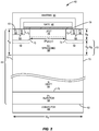
- An exemplary conventional IGBT device 10 is shown in Figure 1 .
- the conventional IGBT device shown in Figure 1 represents a single IGBT cell that includes an IGBT stack 12, a collector contact 14, a gate contact 16, and an emitter contact 18.
- the IGBT stack 12 includes an injector region 20 adjacent to the collector contact 14, a drift region 22 over the injector region 20 and adjacent to the gate contact 16 and the emitter contact 18, and a pair of junction implants 24 in the drift region 22.
- the drift region 22 provides a first surface 26 of the IGBT stack 12 on which the gate contact 16 and the emitter contact 18 are located.
- the injector region 20 provides a second surface 28 of the IGBT stack 12 opposite the first surface 26 on which the collector contact 14 is located.
- Each one of the junction implants 24 is generally formed by an ion implantation process, and includes a base well 30, a source well 32, and an ohmic well 34.
- Each base well 30 is implanted in the first surface 26 of the IGBT stack 12, and extends down towards the injector region 20 along a lateral edge 36 of the IGBT stack 12.
- the source well 32 and the ohmic well 34 are formed in a shallow portion on the first surface 26 of the IGBT stack 12, and are surrounded by the base well 30.
- a JFET gap 38 separates each one of the junction implants 24, and defines a JFET gap width W JFET as the distance between each one of the junction implants 24 in the conventional IGBT device 10.
- a gate oxide layer 40 is positioned on the first surface 26 of the IGBT stack 12, and extends laterally between a portion of the surface of each one of the source wells 32, such that the gate oxide layer 40 partially overlaps and runs between the surface of each source well 32 in the junction implants 24.
- the gate contact 16 is positioned over the gate oxide layer 40.
- the emitter contact 18 is a "U" shape, and includes two portions in contact with the first surface 26 of the IGBT stack 12. Each portion of the emitter contact 18 on the first surface 26 of the IGBT stack 12 partially overlaps both the source well 32 and the ohmic well 34 of one of the junction implants 24, respectively, without contacting the gate contact 16 or the gate oxide layer 40.
- a first junction J 1 between the injector region 20 and the drift region 22, a second junction J 2 between each base well 30 and the drift region 22, and a third junction J 3 between each source well 32 and each base well 30 are controlled to operate in one of a forward-bias mode of operation or a reverse-bias mode of operation based on the biasing of the conventional IGBT device 10. Accordingly, the flow of current between the collector contact 14 and the emitter contact 18 is controlled.
- the conventional IGBT device 10 has three primary modes of operation. When a positive bias is applied to the gate contact 16 and the emitter contact 18, and a negative bias is applied to the collector contact 14, the conventional IGBT device 10 operates in a reverse blocking mode. In the reverse blocking mode of the conventional IGBT device 10, the first junction J 1 and the third junction J 3 are reverse-biased, while the second junction J 2 is forward biased. As will be understood by those of ordinary skill in the art, the reverse-biased junctions J 1 and J 3 prevent current from flowing from the collector contact 14 to the emitter contact 18. Accordingly, the drift region 22 supports the majority of the voltage across the collector contact 14 and the emitter contact 18.
- the conventional IGBT device 10 When a negative bias is applied to the gate contact 16 and the emitter contact 18, and a positive bias is applied to the collector contact 14, the conventional IGBT device 10 operates in a forward blocking mode.
- the first junction J 1 and the third junction J 3 are forward biased, while the second junction J 2 is reverse-biased.
- the reverse-bias of the second junction J 2 generates a depletion region, which effectively pinches off the JFET gap 38 of the IGBT device 10 and prevents current from flowing from the collector contact 14 to the emitter contact 18. Accordingly, the drift region 22 supports the majority of the voltage across the collector contact 14 and the emitter contact 18.
- the conventional IGBT device 10 When a positive bias is applied to the gate contact 16 and the collector contact 14, and a negative bias is applied to the emitter contact 18, the conventional IGBT device 10 operates in a forward conduction mode of operation.
- the first junction J 1 and the third junction J 3 are forward-biased, while the second junction J 2 is reverse-biased. Accordingly, current can flow from the collector contact 14 to the emitter contact 18.
- the positive bias applied to the gate contact 16 generates an inversion channel on the first surface 26 of the IGBT stack 12, thereby creating a low-resistance path for electrons to flow from the emitter contact 18 through each one of the source wells 32 and each one of the base wells 30 into the drift region 22.
- the potential of the drift region 22 is decreased, thereby placing the first junction J 1 in a forward-bias mode of operation.
- the first junction J 1 becomes forward-biased, holes are allowed to flow from the injector region 20 into the drift region 22.
- the holes effectively increase the doping concentration of the drift region 22, thereby increasing the conductivity thereof. Accordingly, electrons from the emitter contact 18 may flow more easily through the drift region 22 and to the collector contact 14.
- the IGBT stack 12 of the conventional IGBT device 10 is Silicon (Si), the advantages and shortcomings of which are well known to those of ordinary skill in the art.
- Si Silicon Carbide
- SiC Silicon Carbide
- conventional IGBT structures such as the one shown in Figure 1 are generally unsuitable for use with wide band-gap materials such as SiC. Due to inherent limitations in SiC fabrication processes, the carrier mobility and/or carrier concentration in the injector region 20 in a SiC IGBT device may be significantly diminished.
- the conductivity in the injector region 20 will be low in a SiC device due to difficulties in growing high quality P-type epitaxial layers with low defect density. Further, due to damage in the drift region 22 caused by the ion implantation of the junction implants 24, the lifetime of carriers in the area directly below each junction implant 24 is significantly diminished. The result of the aforementioned conditions in a SiC IGBT device is that holes from the injector region 20 do not adequately modulate the conductivity of the portion of the drift region 22 above a certain distance from the injector region 20.
- an IGBT structure is needed that is suitable for use with wide band-gap semiconductor materials such as SiC.
- an IGBT device includes an IGBT stack, a collector contact, a gate contact, and an emitter contact.
- the IGBT stack includes an injector region, a drift region over the injector region, a spreading region over the drift region, and a pair of junction implants in the spreading region.
- the spreading region provides a first surface of the IGBT stack, which is opposite the drift region.
- the pair of junction implants is separated by a JFET gap, and extends from the first surface of the IGBT stack along a lateral edge of the IGBT stack towards the drift region to a first depth, such that the thickness of the spreading region is at least two times greater than the first depth.
- the IGBT stack is formed of a wide band-gap semiconductor material.
- the IGBT stack may be a Silicon Carbide (SiC) substrate.
- the drift region is a lightly doped N region
- the injector region is a highly doped P region
- the spreading region is a highly doped N region.
- Figure 1 shows a two-dimensional representation of a conventional IGBT device.
- Figure 2 shows a two-dimensional representation of an IGBT device suitable for wide band-gap semiconductor materials according to one embodiment of the present disclosure.
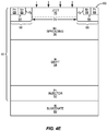
- Figure 3 shows a flow-chart describing a method for manufacturing the IGBT device shown in Figure 2 according to one embodiment of the present disclosure.
- FIGS 4A-4I illustrate the method for manufacturing the IGBT device described in Figure 2 according to one embodiment of the present disclosure.
- Figure 5 shows a two-dimensional representation of an IGBT device suitable for wide band-gap semiconductor materials according to one embodiment of the present disclosure.
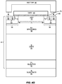
- Figure 6 shows a flow-chart describing a method for manufacturing the IGBT device shown in Figure 5 according to one embodiment of the present disclosure.
- FIGS 7A-7F illustrate the method for manufacturing the IGBT device described in Figure 5 according to one embodiment of the present disclosure.
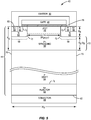
- the IGBT device 42 shown in Figure 2 represents a single IGBT cell, which may be part of a larger IGBT device including multiple cells.
- the IGBT device 42 includes an IGBT stack 44, a collector contact 46, a gate contact 48, and an emitter contact 50.
- the IGBT stack 44 includes an injector region 52 adjacent to the collector contact 46, a drift region 54 over the injector region 52, a spreading region 56 over the drift region 54 and adjacent to the gate contact 48 and the emitter contact 50, and a pair of junction implants 58 in the spreading region 56.
- the spreading region 56 provides a first surface 60 of the IGBT stack 44 on which the gate contact 48 and the emitter contact 50 are located. Further, the injector region 52 provides a second surface 62 of the IGBT stack 44 opposite the first surface 60 on which the collector contact 46 is located. A thickness (Ts) of the spreading region 56 is defined as the distance between the junction of the spreading region 56 and the drift region 54 and the first surface 60 of the IGBT stack 44.
- Each one of the junction implants 58 may be formed by an ion implantation process, and may include a base well 64, a source well 66, and an ohmic well 68.
- Each base well 64 is implanted in the first surface 60 of the IGBT stack 44, and extends down towards the injector region 52 along a lateral edge 70 of the IGBT stack 44 to a first depth (D B ).
- the first depth (D B ) represents the portion of each junction implant 58 that is closest to the drift region 54, which is substantially less than the thickness (Ts) of the spreading region 56, thereby leaving a spreading layer buffer 72 between each one of the junction implants 58 and the drift region 54 in order to mitigate the effects of one or more damaged regions located below the junction implants 58, as discussed in further detail below.
- the thickness of the spreading layer buffer 72 is the thickness (Ts) of the spreading region 56 less the first depth (D B ) of the base well 64.
- the source well 66 and the ohmic well 68 are formed in a shallow portion of the first surface 60 of the IGBT stack 44, and are surrounded by the base well 64.
- a JFET gap 74 separates each one of the junction implants 58, and defines a JFET gap width W JFET as the distance between each one of the junction implants in the IGBT device 42.
- An additional junction field-effect transistor (JFET) implant 76 may be provided in the JFET gap 74, as discussed in further detail below.
- the thickness (Ts) of the spreading region 56 is between about 1.5 ⁇ m to 10 ⁇ m.
- the first depth (D B ) of the base well 64 may be between about 0.5 ⁇ m to 1.5 ⁇ m.
- the thickness (Ts) of the spreading region 56 is two times greater than the first depth (D B ) of the base well 64 of each junction implant 58 in order to provide the spreading layer buffer 72, which mitigates the effects of one or more damaged regions located below the junction implants 58.
- the thickness (Ts) of the spreading region 56 may be at least 1.5 ⁇ m to 10.0 ⁇ m greater than the first depth (D B ) of the base wells 64, such that the spreading layer buffer 72 is at least 1.5 ⁇ m to 10.0 ⁇ m.
- a gate oxide layer 78 may be positioned on the first surface 60 of the IGBT stack 44, and may extend laterally between a portion of the surface of each one of the source wells 66, such that the gate oxide layer 78 partially overlaps and runs between the surface of each source well 66 in the junction implants 58.
- the emitter contact 50 may be a "U" shape, and may include two portions in contact with the first surface 60 of the IGBT stack 44. Each portion of the emitter contact 50 on the first surface 60 of the IGBT stack 44 may partially overlap both the source well 66 and the ohmic well 68 of one of the junction implants 58, respectively, without contacting the gate contact 48 of the gate oxide layer 78.
- a first junction J 1 between the injector region 52 and the drift region 54, a second junction J 2 between each base well 64 and the drift region 54, and a third junction J 3 between each source well 66 and each base well 64 are controlled to operate in one of a forward-bias mode of operation or a reverse-bias mode of operation based on the biasing of the IGBT device 42. Accordingly, the flow of current between the collector contact 46 and the emitter contact 50 is controlled.
- the injector region 52 is a highly doped P region 52 with a doping concentration between 1E16 cm -3 to 1E21 cm -3 .
- the drift region 54 may be a lightly doped N region with a doping concentration between 1E13 cm -3 to 1E15 cm -3 .
- the drift region 54 may include a notably light concentration of dopants, in order to improve one or more performance parameters of the IGBT device 42 as discussed in further detail below.
- the spreading region 56 may be a highly doped N region with a doping concentration between 5E15 cm -3 to 5E16 cm -3 .
- the spreading region 56 includes a graduated doping concentration, such that as the spreading region 56 extends away from the first surface 60 of the IGBT stack 44, the doping concentration of the spreading region 56 gradually decreases.
- the portion of the spreading region 56 directly adjacent to the first surface 60 of the IGBT stack 44 may be doped at a concentration of about 5E16 cm -3
- the portion of the spreading region directly adjacent to the drift region 54 may be doped at a concentration of about 5E15 cm -3
- the JFET region 76 may be also be a highly doped N region with a doping concentration between 1E16 cm -3 to 1E17 cm -3 .
- the base well 64 may be a P doped region with a doping concentration between 5E17 cm -3 and 1E19 cm -3
- the source well 66 may be a highly doped N region with a doping concentration between 1 E19 cm -3 and 1 E21 cm -3
- the ohmic well 68 may be a highly doped P layer with a doping concentration between 1 E19 cm -3 and 1 E21 cm -3 .
- the injector region 52 may be doped aluminum, boron, or the like. Those of ordinary skill in the art will appreciate that many different dopants exist that may be suitable for doping the injector region 52, all of which are contemplated herein.
- the drift region 54, the spreading region 56, and the JFET region 76 may be doped with nitrogen, phosphorous, or the like. Those of ordinary skill in the art will appreciate that many different dopants exist that may be suitable for doping the drift region 54, the spreading region 56, and the JFET region, all of which are contemplated herein.
- the injector region 52 is generated by an epitaxy process. According to an additional embodiment, the injector region 52 is formed by an ion implantation process. Those of ordinary skill in the art will appreciate that numerous different processes exist for generating the injector region 52, all of which are contemplated herein.
- the spreading region 56 and the JFET region 76 may similarly be formed by either an epitaxy process or an ion implantation process. Those of ordinary skill in the art will appreciate that numerous different processes exist for generating the spreading region 56 and the JFET region 76, all of which are contemplated herein.
- the IGBT stack 44 is a wide band-gap semiconductor material.
- the IGBT stack 44 may be Silicon Carbide (SiC).
- SiC Silicon Carbide
- manufacturing limitations inherent in current SiC technologies will generally result in a diminished carrier lifetimes and/or carrier concentration in the injector region of a SiC IGBT device.
- SiC IGBT devices generally suffer from a reduced amount of "backside injection", which results in poor conductivity modulation and an increased ON resistance (R ON ) of the SiC IGBT device.
- the introduction of the spreading region 56 also results in a decrease in the blocking voltage (V BLK ) of the IGBT device 42.
- the doping concentration in the drift region 54 may be decreased, such that the doping concentration in the drift region 54 is exceptionally light, as discussed above. Accordingly, a balance between the on resistance (R ON ) and the blocking voltage (V BLK ) of the IGBT device 42 may be struck.
- the IGBT device 42 further benefits from the predominant use of "front-side" injection. That is, the IGBT device 42 shown in Figure 2 transfers current from the collector contact 46 to the emitter contact 50 primarily through the use of electrons supplied from the emitter contact 50, rather than as a result of hole injection from the injector region 52.
- the use of predominant backside injection as is common among conventional IGBT devices, often results in significant switching losses, thereby degrading the performance of the IGBT device. Accordingly, numerous techniques have been developed to reduce the amount of hole injection provided at the back-side of the device, while simultaneously increasing the amount of electrons supplied from the emitter contact. Due to the arrangement of the various regions in the IGBT stack 44, the IGBT device 42 inherently operates in a predominant "front-side" injection mode, thereby improving the performance of the device.
- the spreading region 56 also allows the JFET gap width (W JFET ) and the overall device width (W D ) to be significantly reduced when compared to conventional IGBT devices.
- the JFET gap width (W JFET ) of the IGBT device 42 may be between 1 ⁇ m to 4 ⁇ m, and the overall device width (W D ) of the IGBT device 42 may be between 5 ⁇ m to 15 ⁇ m.
- the spreading region 56 results in desirable thermal properties of the IGBT device 42.
- conventional IGBT devices generally suffer from a significant amount of temperature dependence. That is, the performance characteristics of a conventional IGBT generally change with temperature. Specifically, as the temperature of an IGBT device increases, so does the lifetime of carriers in the drift region, thereby resulting in increased current flow through the device. This can result in a dangerous cycle, in which increased current flow through the IGBT device further raises the temperature of the device, until the IGBT device can no longer handle the amount of current through the device and fails.
- this unmodulated region has an inverse relationship between the current flow therein and temperature.
- FIGs 3 and 4A-4I illustrate a method for manufacturing the IGBT device 42 shown in Figure 2 according to one embodiment of the present disclosure.
- the injector region 52 is grown via an epitaxy process on a sacrificial substrate 80 (step 100 and Figure 4A ).
- the sacrificial substrate 80 must be used to generate the IGBT device 42 shown in Figure 2 due to a lack of available P-substrates for SiC materials systems.
- the drift region 54 is then grown on top of the injector region 52 opposite the substrate 80 (step 102 and Figure 4B ).
- the spreading region 56 is grown via an epitaxy process over the drift region 54 opposite the injector region 52 (step 104 and Figure 4C ).
- the spreading region 56 provides the first surface 60, which is opposite the drift region 54.
- the junction implants 58 are then provided in the first surface 60 of the IGBT stack 44 (step 106 and Figure 4D ), such that the junction implants 58 extend to a first depth D B from the first surface 60 of the IGBT stack 44.
- the junction implants 58 are generally provided via one or more ion implantation processes, however, any suitable method may be used to provide the junction implants 58 without departing from the principles disclosed herein.
- the spreading region 56 and the junction implants 58 are provided such that the spreading region 56 has a thickness Ts that is two times greater than the first depth D B , thereby improving the performance of the completed IGBT device 42.
- the JFET region 76 is then provided in the channel 74 between the junction implants 58 (step 108 and Figure 4E ).
- the JFET region 76 may be provided by an epitaxy process, an ion implantation process, or any other suitable process.
- the gate oxide 78 and the gate contact 48 are provided on the first surface 60 of the IGBT stack 44 (step 110 and Figure 4F ). Specifically, the gate oxide 78 is provided such that the gate oxide 78 partially overlaps and runs between each source well 66 in the pair of junction implants 58, and the gate contact 48 is provided on top of the gate oxide layer 78.
- the emitter contact 50 is then provided on the first surface 60 of the IGBT stack 44 (step 112 and Figure 4G ). Specifically, the emitter contact 50 is provided such that the emitter partially overlaps the source well 66 and the ohmic well 68 in each one of the pair of junction implants 58, respectively, without contacting the gate contact 48.
- the emitter contact 50 may be provided by any suitable metallization process.
- the substrate 80 is removed from the IGBT stack 44 (step 114 and Figure 4H ). The substrate 80 may be removed, for example, by an etching or grinding process.
- the collector contact 46 is provided over the entire second surface 62 of the IGBT stack 44 (step 116 and Figure 4I ). The collector contact 46 may be provided by any suitable metallization process.
- FIG. 5 shows the IGBT device 42 according to an additional embodiment of the present disclosure. While the IGBT device 42 shown above with respect to Figure 2 is an N-IGBT, the IGBT device 42 of Figure 5 is a P-IGBT device. Accordingly, the doping of each one of the separate regions in the IGBT device 42 are the opposite of that shown in Figure 2 , such that the injector region 52 may be a heavily doped N region with a doping concentration between 1E18 cm -3 and 1E21 cm -3 , the drift region 54 may be a lightly doped P region with a doping concentration between 1E13 cm -3 and 1E15 cm -3 , the spreading region 56 may be a heavily doped P region with a doping concentration between 5E15 cm -3 to 5E16 cm -3 , and the JFET region 76 may be a highly doped P region with a doping concentration between 1E16 cm -3 and 1E17 cm -3 .
- the injector region 52 may be a heavily doped N region with
- the base well 64 may be an N doped region with a doping concentration between 5E17 cm -3 and 1E19 cm -3
- the source well 66 may be a highly doped P region with a doping concentration between 1E19 cm -3 and 1E21 cm -3
- the ohmic well 68 may be a highly doped N layer with a doping concentration between 1E19 cm -3 and 1E21 cm -3 .
- the IGBT device 42 shown in Figure 5 may function substantially similarly to the IGBT device 42 described above with respect to Figure 2 , with differences that will be readily appreciated by those of ordinary skill in the art.
- FIGs 6 and 7A-7F illustrate a method for manufacturing the IGBT device 42 shown in Figure 5 according to one embodiment of the present disclosure.
- the drift region 54 is grown on top of the injector region 52 (step 200 and Figure 7A ).
- the injector region can serve as the substrate for growing the other regions in the IGBT stack 44.
- the spreading region 56 is then grown on top of the drift region 54 opposite the injector region 52 (step 202 and Figure 7B ).
- the spreading region 56 provides the first surface 60, which is opposite the IGBT stack 44.
- the junction implants 58 are provided in the first surface 60 of the IGBT stack 44 (step 204 and Figure 7C ), such that the junction implants 58 extend to a first depth D B from the first surface 60 of the IGBT stack 44.
- the junction implants 58 are generally provided via one or more implantation processes, however, any suitable method may be used to provide the junction implants 58 without departing from the principles disclosed herein.
- the spreading region 56 and the junction implants 58 are provided such that the spreading region 56 has a thickness Ts that is two times greater than the first depth D B , thereby improving the performance of the completed IGBT device 42.
- the JFET region 76 is then provided in the channel 74 between the junction implants 58 (step 206 and Figure 7D ).
- the JFET region 76 may be provided by an epitaxy process, an ion implantation process, or any other suitable process.
- the gate oxide 78 and the gate contact 48 are provided on the first surface 60 of the IGBT stack 44 (step 208 and Figure 7E ). Specifically, the gate oxide 78 is provided such that the gate oxide 78 partially overlaps and runs between each source well 66 in the pair of junction implants 58, and the gate contact 48 is provided on top of the gate oxide layer 78.
- the collector contact 46 is provided on the second surface 62 of the IGBT stack 44, and the emitter contact 50 is provided on the first surface 60 of the IGBT stack 44 (step 210 and Figure 4F ).
- the emitter contact 50 is provided such that the emitter contact 50 partially overlaps the source well 66 and the ohmic well 68 in each one of the pair of junction implants, respectively, without contacting the gate contact 48, while the collector contact 46 is provided over the entire second surface 62 of the IGBT stack 44.
- the collector contact 46 and the emitter contact 50 may be provided by any suitable metallization process.
Description
- The present disclosure relates to insulated gate bipolar transistor (IGBT) devices and structures.
-
EP 1965432 discloses an IGBT comprising: a substrate having a first conductivity type; a drift layer on the substrate and having a second conductivity type opposite the first conductivity type; a current suppressing layer on the drift layer, the current suppressing layer having the second conductivity type and having a doping concentration that is larger than a doping concentration of the drift layer; a well region in the current suppressing layer and having the first conductivity type, wherein the well region has a junction depth that is less than a thickness of the current suppressing layer, and wherein the current suppressing layer extends laterally beneath the well region; and an emitter region in the well region and having the second conductivity type. - Insulated gate bipolar transistors devices, i.e. IGBT, provided with current suppressing layers are also known from the documents
US 2012/0292742 A1 ,US 2011/0101375 A1 ,US 2004/0119076 A1 ,EP 2 581 939 A2 and from a non patent literature "Optimization of on -State and Switching Performances for 15-20-kV 4H-SiC IGBTs", Tamaki T. et al, published in IEEE Transactions on Electron Devices, Volume: 55, Issue: 8, Aug. 2008. - Document
GB 2 243 952 A conventional IGBT device 10 is shown inFigure 1 . The conventional IGBT device shown inFigure 1 represents a single IGBT cell that includes anIGBT stack 12, acollector contact 14, agate contact 16, and anemitter contact 18. TheIGBT stack 12 includes aninjector region 20 adjacent to thecollector contact 14, adrift region 22 over theinjector region 20 and adjacent to thegate contact 16 and theemitter contact 18, and a pair ofjunction implants 24 in thedrift region 22. Thedrift region 22 provides afirst surface 26 of theIGBT stack 12 on which thegate contact 16 and theemitter contact 18 are located. Further, theinjector region 20 provides asecond surface 28 of theIGBT stack 12 opposite thefirst surface 26 on which thecollector contact 14 is located. - Each one of the
junction implants 24 is generally formed by an ion implantation process, and includes a base well 30, a source well 32, and anohmic well 34. Each base well 30 is implanted in thefirst surface 26 of theIGBT stack 12, and extends down towards theinjector region 20 along alateral edge 36 of theIGBT stack 12. The source well 32 and theohmic well 34 are formed in a shallow portion on thefirst surface 26 of theIGBT stack 12, and are surrounded by the base well 30. AJFET gap 38 separates each one of thejunction implants 24, and defines a JFET gap width WJFET as the distance between each one of thejunction implants 24 in theconventional IGBT device 10. - A
gate oxide layer 40 is positioned on thefirst surface 26 of theIGBT stack 12, and extends laterally between a portion of the surface of each one of thesource wells 32, such that thegate oxide layer 40 partially overlaps and runs between the surface of each source well 32 in thejunction implants 24. Thegate contact 16 is positioned over thegate oxide layer 40. Theemitter contact 18 is a "U" shape, and includes two portions in contact with thefirst surface 26 of theIGBT stack 12. Each portion of the emitter contact 18 on thefirst surface 26 of theIGBT stack 12 partially overlaps both the source well 32 and theohmic well 34 of one of thejunction implants 24, respectively, without contacting thegate contact 16 or thegate oxide layer 40. - A first junction J1 between the
injector region 20 and thedrift region 22, a second junction J2 between each base well 30 and thedrift region 22, and a third junction J3 between each source well 32 and eachbase well 30 are controlled to operate in one of a forward-bias mode of operation or a reverse-bias mode of operation based on the biasing of theconventional IGBT device 10. Accordingly, the flow of current between thecollector contact 14 and theemitter contact 18 is controlled. - The
conventional IGBT device 10 has three primary modes of operation. When a positive bias is applied to thegate contact 16 and theemitter contact 18, and a negative bias is applied to thecollector contact 14, theconventional IGBT device 10 operates in a reverse blocking mode. In the reverse blocking mode of theconventional IGBT device 10, the first junction J1 and the third junction J3 are reverse-biased, while the second junction J2 is forward biased. As will be understood by those of ordinary skill in the art, the reverse-biased junctions J1 and J3 prevent current from flowing from thecollector contact 14 to theemitter contact 18. Accordingly, thedrift region 22 supports the majority of the voltage across thecollector contact 14 and theemitter contact 18. - When a negative bias is applied to the
gate contact 16 and theemitter contact 18, and a positive bias is applied to thecollector contact 14, theconventional IGBT device 10 operates in a forward blocking mode. In the forward blocking mode of theconventional IGBT device 10, the first junction J1 and the third junction J3 are forward biased, while the second junction J2 is reverse-biased. As will be understood by those of ordinary skill in the art, the reverse-bias of the second junction J2 generates a depletion region, which effectively pinches off theJFET gap 38 of theIGBT device 10 and prevents current from flowing from thecollector contact 14 to theemitter contact 18. Accordingly, thedrift region 22 supports the majority of the voltage across thecollector contact 14 and theemitter contact 18. - When a positive bias is applied to the
gate contact 16 and thecollector contact 14, and a negative bias is applied to theemitter contact 18, theconventional IGBT device 10 operates in a forward conduction mode of operation. In the forward conduction mode of operation of theconventional IGBT device 10, the first junction J1 and the third junction J3 are forward-biased, while the second junction J2 is reverse-biased. Accordingly, current can flow from thecollector contact 14 to theemitter contact 18. Specifically, the positive bias applied to thegate contact 16 generates an inversion channel on thefirst surface 26 of theIGBT stack 12, thereby creating a low-resistance path for electrons to flow from theemitter contact 18 through each one of thesource wells 32 and each one of thebase wells 30 into thedrift region 22. As electrons flow into thedrift region 22, the potential of thedrift region 22 is decreased, thereby placing the first junction J1 in a forward-bias mode of operation. When the first junction J1 becomes forward-biased, holes are allowed to flow from theinjector region 20 into thedrift region 22. The holes effectively increase the doping concentration of thedrift region 22, thereby increasing the conductivity thereof. Accordingly, electrons from theemitter contact 18 may flow more easily through thedrift region 22 and to the collector contact 14. - The
IGBT stack 12 of theconventional IGBT device 10 is Silicon (Si), the advantages and shortcomings of which are well known to those of ordinary skill in the art. In an attempt to further increase the performance of IGBT devices, many have focused their efforts on using wide band-gap materials such as Silicon Carbide (SiC) for theIGBT stack 12. Although promising, conventional IGBT structures such as the one shown inFigure 1 are generally unsuitable for use with wide band-gap materials such as SiC. Due to inherent limitations in SiC fabrication processes, the carrier mobility and/or carrier concentration in theinjector region 20 in a SiC IGBT device may be significantly diminished. Specifically, the conductivity in theinjector region 20 will be low in a SiC device due to difficulties in growing high quality P-type epitaxial layers with low defect density. Further, due to damage in thedrift region 22 caused by the ion implantation of thejunction implants 24, the lifetime of carriers in the area directly below eachjunction implant 24 is significantly diminished. The result of the aforementioned conditions in a SiC IGBT device is that holes from theinjector region 20 do not adequately modulate the conductivity of the portion of thedrift region 22 above a certain distance from theinjector region 20. Accordingly, electrons from theemitter contact 18 are met with a high-resistance path in the upper portion of thedrift region 22, thereby increasing the on resistance RON of theconventional IGBT device 10 significantly, or cutting off current flow in the device altogether. Accordingly, an IGBT structure is needed that is suitable for use with wide band-gap semiconductor materials such as SiC. - The present disclosure relates to an insulated gate bipolar transistor (IGBT) according to claim 1. According to one embodiment, an IGBT device includes an IGBT stack, a collector contact, a gate contact, and an emitter contact. The IGBT stack includes an injector region, a drift region over the injector region, a spreading region over the drift region, and a pair of junction implants in the spreading region. The spreading region provides a first surface of the IGBT stack, which is opposite the drift region. The pair of junction implants is separated by a JFET gap, and extends from the first surface of the IGBT stack along a lateral edge of the IGBT stack towards the drift region to a first depth, such that the thickness of the spreading region is at least two times greater than the first depth. By including the spreading layer that is substantially thicker than the depth of each junction implant, the ON resistance RON and front-side injection capabilities of the IGBT device may be improved.
- According to one embodiment, the IGBT stack is formed of a wide band-gap semiconductor material. For example, the IGBT stack may be a Silicon Carbide (SiC) substrate.
- According to one embodiment, the drift region is a lightly doped N region, the injector region is a highly doped P region, and the spreading region is a highly doped N region.
- Those skilled in the art will appreciate the scope of the present disclosure and realize additional aspects thereof after reading the following detailed description of the preferred embodiments in association with the accompanying drawing figures.
- The accompanying drawing figures incorporated in and forming a part of this specification illustrate several aspects of the disclosure, and together with the description serve to explain the principles of the disclosure.
-
Figure 1 shows a two-dimensional representation of a conventional IGBT device. -
Figure 2 shows a two-dimensional representation of an IGBT device suitable for wide band-gap semiconductor materials according to one embodiment of the present disclosure. -
Figure 3 shows a flow-chart describing a method for manufacturing the IGBT device shown inFigure 2 according to one embodiment of the present disclosure. -
Figures 4A-4I illustrate the method for manufacturing the IGBT device described inFigure 2 according to one embodiment of the present disclosure. -
Figure 5 shows a two-dimensional representation of an IGBT device suitable for wide band-gap semiconductor materials according to one embodiment of the present disclosure. -
Figure 6 shows a flow-chart describing a method for manufacturing the IGBT device shown inFigure 5 according to one embodiment of the present disclosure. -
Figures 7A-7F illustrate the method for manufacturing the IGBT device described inFigure 5 according to one embodiment of the present disclosure. - The embodiments set forth below represent the necessary information to enable those skilled in the art to practice the embodiments and illustrate the best mode of practicing the embodiments. Upon reading the following description in light of the accompanying drawing figures, those skilled in the art will understand the concepts of the disclosure and will recognize applications of these concepts not particularly addressed herein. It should be understood that these concepts and applications fall within the scope of the disclosure and the accompanying claims.
- It will be understood that, although the terms first, second, etc. may be used herein to describe various elements, these elements should not be limited by these terms. These terms are only used to distinguish one element from another. For example, a first element could be termed a second element, and, similarly, a second element could be termed a first element, without departing from the scope of the present disclosure. As used herein, the term "and/or" includes any and all combinations of one or more of the associated listed items.
- It will be understood that when an element such as a layer, region, or substrate is referred to as being "on" or extending "onto" another element, it can be directly on or extend directly onto the other element or intervening elements may also be present. In contrast, when an element is referred to as being "directly on" or extending "directly onto" another element, there are no intervening elements present. Likewise, it will be understood that when an element such as a layer, region, or substrate is referred to as being "over" or extending "over" another element, it can be directly over or extend directly over the other element or intervening elements may also be present. In contrast, when an element is referred to as being "directly over" or extending "directly over" another element, there are no intervening elements present. It will also be understood that when an element is referred to as being "connected" or "coupled" to another element, it can be directly connected or coupled to the other element or intervening elements may be present. In contrast, when an element is referred to as being "directly connected" or "directly coupled" to another element, there are no intervening elements present.
- Relative terms such as "below" or "above" or "upper" or "lower" or "horizontal" or "vertical" may be used herein to describe a relationship of one element, layer, or region to another element, layer, or region as illustrated in the
- Figures. It will be understood that these terms and those discussed above are intended to encompass different orientations of the device in addition to the orientation depicted in the Figures.
- The terminology used herein is for the purpose of describing particular embodiments only and is not intended to be limiting of the disclosure. As used herein, the singular forms "a," "an," and "the" are intended to include the plural forms as well, unless the context clearly indicates otherwise. It will be further understood that the terms "comprises," "comprising," "includes," and/or "including" when used herein specify the presence of stated features, integers, steps, operations, elements, and/or components, but do not preclude the presence or addition of one or more other features, integers, steps, operations, elements, components, and/or groups thereof.
- Unless otherwise defined, all terms (including technical and scientific terms) used herein have the same meaning as commonly understood by one of ordinary skill in the art to which this disclosure belongs. It will be further understood that terms used herein should be interpreted as having a meaning that is consistent with their meaning in the context of this specification and the relevant art and will not be interpreted in an idealized or overly formal sense unless expressly so defined herein.
- Turning now to
Figure 2 , anIGBT device 42 suitable for use with wide band-gap semiconductor materials systems is shown according to one embodiment of the present disclosure. TheIGBT device 42 shown inFigure 2 represents a single IGBT cell, which may be part of a larger IGBT device including multiple cells. TheIGBT device 42 includes anIGBT stack 44, acollector contact 46, agate contact 48, and anemitter contact 50. TheIGBT stack 44 includes aninjector region 52 adjacent to thecollector contact 46, adrift region 54 over theinjector region 52, a spreadingregion 56 over thedrift region 54 and adjacent to thegate contact 48 and theemitter contact 50, and a pair ofjunction implants 58 in the spreadingregion 56. The spreadingregion 56 provides afirst surface 60 of theIGBT stack 44 on which thegate contact 48 and theemitter contact 50 are located. Further, theinjector region 52 provides asecond surface 62 of theIGBT stack 44 opposite thefirst surface 60 on which thecollector contact 46 is located. A thickness (Ts) of the spreadingregion 56 is defined as the distance between the junction of the spreadingregion 56 and thedrift region 54 and thefirst surface 60 of theIGBT stack 44. - Each one of the
junction implants 58 may be formed by an ion implantation process, and may include a base well 64, a source well 66, and anohmic well 68. Each base well 64 is implanted in thefirst surface 60 of theIGBT stack 44, and extends down towards theinjector region 52 along alateral edge 70 of theIGBT stack 44 to a first depth (DB). Notably, the first depth (DB) represents the portion of eachjunction implant 58 that is closest to thedrift region 54, which is substantially less than the thickness (Ts) of the spreadingregion 56, thereby leaving a spreadinglayer buffer 72 between each one of thejunction implants 58 and thedrift region 54 in order to mitigate the effects of one or more damaged regions located below thejunction implants 58, as discussed in further detail below. The thickness of the spreadinglayer buffer 72 is the thickness (Ts) of the spreadingregion 56 less the first depth (DB) of the base well 64. The source well 66 and theohmic well 68 are formed in a shallow portion of thefirst surface 60 of theIGBT stack 44, and are surrounded by the base well 64. AJFET gap 74 separates each one of thejunction implants 58, and defines a JFET gap width WJFET as the distance between each one of the junction implants in theIGBT device 42. An additional junction field-effect transistor (JFET)implant 76 may be provided in theJFET gap 74, as discussed in further detail below. - According to one embodiment, the thickness (Ts) of the spreading
region 56 is between about 1.5 µm to 10 µm. The first depth (DB) of the base well 64 may be between about 0.5 µm to 1.5 µm. As discussed in further detail below, the thickness (Ts) of the spreadingregion 56 is two times greater than the first depth (DB) of the base well 64 of eachjunction implant 58 in order to provide the spreadinglayer buffer 72, which mitigates the effects of one or more damaged regions located below thejunction implants 58.
As an additional example, the thickness (Ts) of the spreadingregion 56 may be at least 1.5 µm to 10.0 µm greater than the first depth (DB) of thebase wells 64, such that the spreadinglayer buffer 72 is at least 1.5 µm to 10.0 µm. - A
gate oxide layer 78 may be positioned on thefirst surface 60 of theIGBT stack 44, and may extend laterally between a portion of the surface of each one of thesource wells 66, such that thegate oxide layer 78 partially overlaps and runs between the surface of each source well 66 in thejunction implants 58. Theemitter contact 50 may be a "U" shape, and may include two portions in contact with thefirst surface 60 of theIGBT stack 44. Each portion of theemitter contact 50 on thefirst surface 60 of theIGBT stack 44 may partially overlap both the source well 66 and the ohmic well 68 of one of thejunction implants 58, respectively, without contacting thegate contact 48 of thegate oxide layer 78. - A first junction J1 between the
injector region 52 and thedrift region 54, a second junction J2 between each base well 64 and thedrift region 54, and a third junction J3 between each source well 66 and each base well 64 are controlled to operate in one of a forward-bias mode of operation or a reverse-bias mode of operation based on the biasing of theIGBT device 42. Accordingly, the flow of current between thecollector contact 46 and theemitter contact 50 is controlled. - According to one embodiment, the
injector region 52 is a highly dopedP region 52 with a doping concentration between 1E16 cm-3 to 1E21 cm-3. Thedrift region 54 may be a lightly doped N region with a doping concentration between 1E13 cm-3 to 1E15 cm-3. In some embodiments, thedrift region 54 may include a notably light concentration of dopants, in order to improve one or more performance parameters of theIGBT device 42 as discussed in further detail below. The spreadingregion 56 may be a highly doped N region with a doping concentration between 5E15 cm-3 to 5E16 cm-3. The spreadingregion 56 includes a graduated doping concentration, such that as the spreadingregion 56 extends away from thefirst surface 60 of theIGBT stack 44, the doping concentration of the spreadingregion 56 gradually decreases. For example, the portion of the spreadingregion 56 directly adjacent to thefirst surface 60 of theIGBT stack 44 may be doped at a concentration of about 5E16 cm-3, while the portion of the spreading region directly adjacent to thedrift region 54 may be doped at a concentration of about 5E15 cm-3. TheJFET region 76 may be also be a highly doped N region with a doping concentration between 1E16 cm-3 to 1E17 cm-3. Further, the base well 64 may be a P doped region with a doping concentration between 5E17 cm-3 and 1E19 cm-3, the source well 66 may be a highly doped N region with a doping concentration between 1 E19 cm-3 and 1 E21 cm-3, and theohmic well 68 may be a highly doped P layer with a doping concentration between 1 E19 cm-3 and 1 E21 cm-3. - The
injector region 52 may be doped aluminum, boron, or the like. Those of ordinary skill in the art will appreciate that many different dopants exist that may be suitable for doping theinjector region 52, all of which are contemplated herein. Thedrift region 54, the spreadingregion 56, and theJFET region 76 may be doped with nitrogen, phosphorous, or the like. Those of ordinary skill in the art will appreciate that many different dopants exist that may be suitable for doping thedrift region 54, the spreadingregion 56, and the JFET region, all of which are contemplated herein. - According to one embodiment, the
injector region 52 is generated by an epitaxy process. According to an additional embodiment, theinjector region 52 is formed by an ion implantation process. Those of ordinary skill in the art will appreciate that numerous different processes exist for generating theinjector region 52, all of which are contemplated herein. The spreadingregion 56 and theJFET region 76 may similarly be formed by either an epitaxy process or an ion implantation process. Those of ordinary skill in the art will appreciate that numerous different processes exist for generating the spreadingregion 56 and theJFET region 76, all of which are contemplated herein. - According to one embodiment, the
IGBT stack 44 is a wide band-gap semiconductor material. For example, theIGBT stack 44 may be Silicon Carbide (SiC). As discussed above, manufacturing limitations inherent in current SiC technologies will generally result in a diminished carrier lifetimes and/or carrier concentration in the injector region of a SiC IGBT device. As a result, SiC IGBT devices generally suffer from a reduced amount of "backside injection", which results in poor conductivity modulation and an increased ON resistance (RON) of the SiC IGBT device. Further, in attempting to design a wide band-gap IGBT device, it was discovered by the inventors that damaged regions below each one of the junction implants of a SiC IGBT device result in a significantly degraded carrier lifetime at or near these damaged regions. These so-called "end-of-range" defects effectively prevent the modulation of current in the upper portion of the drift layer in a SiC IGBT device, which in turn significantly increases the resistance in this area. As a result of the increased resistance in the upper portion of the drift region, current flow in the SiC IGBT device may be significantly reduced, and may even be cut off altogether. The spreadingregion 56 of theIGBT device 42 is therefore provided to bypass the damaged regions below each one of thejunction implants 58, thereby improving the performance of theSiC IGBT device 42. - By bypassing the damaged regions below each one of the
junction implants 58, electrons from theemitter contact 50 are delivered directly to a region of high conductivity modulation in thedrift region 54. Accordingly, electrons easily pass into thedrift region 54 and to thecollector contact 46 of theIGBT device 42. Those of ordinary skill in the art will recognize that the ON resistance (RON) is significantly reduced in theIGBT device 42, thereby improving the performance thereof. - While the spreading
region 56 effectively reduces the ON resistance (RON) of theIGBT device 42, the introduction of the spreadingregion 56 also results in a decrease in the blocking voltage (VBLK) of theIGBT device 42. In order to compensate for this fact, the doping concentration in thedrift region 54 may be decreased, such that the doping concentration in thedrift region 54 is exceptionally light, as discussed above. Accordingly, a balance between the on resistance (RON) and the blocking voltage (VBLK) of theIGBT device 42 may be struck. - In addition to the advantages described above, the
IGBT device 42 further benefits from the predominant use of "front-side" injection. That is, theIGBT device 42 shown inFigure 2 transfers current from thecollector contact 46 to theemitter contact 50 primarily through the use of electrons supplied from theemitter contact 50, rather than as a result of hole injection from theinjector region 52. As will be appreciated by those of ordinary skill in the art, the use of predominant backside injection, as is common among conventional IGBT devices, often results in significant switching losses, thereby degrading the performance of the IGBT device. Accordingly, numerous techniques have been developed to reduce the amount of hole injection provided at the back-side of the device, while simultaneously increasing the amount of electrons supplied from the emitter contact. Due to the arrangement of the various regions in theIGBT stack 44, theIGBT device 42 inherently operates in a predominant "front-side" injection mode, thereby improving the performance of the device. - Further, providing the spreading
region 56 also allows the JFET gap width (WJFET) and the overall device width (WD) to be significantly reduced when compared to conventional IGBT devices. For example, the JFET gap width (WJFET) of theIGBT device 42 may be between 1 µm to 4 µm, and the overall device width (WD) of theIGBT device 42 may be between 5 µm to 15 µm. - Finally, providing the spreading
region 56 results in desirable thermal properties of theIGBT device 42. As will be appreciated by those of ordinary skill in the art, conventional IGBT devices generally suffer from a significant amount of temperature dependence. That is, the performance characteristics of a conventional IGBT generally change with temperature. Specifically, as the temperature of an IGBT device increases, so does the lifetime of carriers in the drift region, thereby resulting in increased current flow through the device. This can result in a dangerous cycle, in which increased current flow through the IGBT device further raises the temperature of the device, until the IGBT device can no longer handle the amount of current through the device and fails. By providing the spreadingregion 56 in theIGBT device 42, a large unmodulated region is generated below thefirst surface 60 of theIGBT stack 44, as discussed above. As will be appreciated by those of ordinary skill in the art, this unmodulated region has an inverse relationship between the current flow therein and temperature. By carefully choosing the dimensions of thedrift region 54 and the spreadingregion 56, a designer can thus effectively cancel the effects of temperature on current flow in theIGBT device 42, thereby significantly increasing the performance thereof. -
Figures 3 and4A-4I illustrate a method for manufacturing theIGBT device 42 shown inFigure 2 according to one embodiment of the present disclosure. First, theinjector region 52 is grown via an epitaxy process on a sacrificial substrate 80 (step 100 andFigure 4A ). As will be appreciated by those of ordinary skill in the art, thesacrificial substrate 80 must be used to generate theIGBT device 42 shown inFigure 2 due to a lack of available P-substrates for SiC materials systems. Thedrift region 54 is then grown on top of theinjector region 52 opposite the substrate 80 (step 102 andFigure 4B ). Next, the spreadingregion 56 is grown via an epitaxy process over thedrift region 54 opposite the injector region 52 (step 104 andFigure 4C ). The spreadingregion 56 provides thefirst surface 60, which is opposite thedrift region 54. Thejunction implants 58 are then provided in thefirst surface 60 of the IGBT stack 44 (step 106 andFigure 4D ), such that thejunction implants 58 extend to a first depth DB from thefirst surface 60 of theIGBT stack 44. Thejunction implants 58 are generally provided via one or more ion implantation processes, however, any suitable method may be used to provide thejunction implants 58 without departing from the principles disclosed herein. Notably, as discussed above, the spreadingregion 56 and thejunction implants 58 are provided such that the spreadingregion 56 has a thickness Ts that is two times greater than the first depth DB, thereby improving the performance of the completedIGBT device 42. - The
JFET region 76 is then provided in thechannel 74 between the junction implants 58 (step 108 andFigure 4E ). TheJFET region 76 may be provided by an epitaxy process, an ion implantation process, or any other suitable process. Next, thegate oxide 78 and thegate contact 48 are provided on thefirst surface 60 of the IGBT stack 44 (step 110 andFigure 4F ). Specifically, thegate oxide 78 is provided such that thegate oxide 78 partially overlaps and runs between each source well 66 in the pair ofjunction implants 58, and thegate contact 48 is provided on top of thegate oxide layer 78. As will be appreciated by those of ordinary skill in the art, several different oxidation and metallization techniques exist for providing thegate oxide 78 and thegate contact 48, respectively, all of which are contemplated herein. Theemitter contact 50 is then provided on thefirst surface 60 of the IGBT stack 44 (step 112 andFigure 4G ). Specifically, theemitter contact 50 is provided such that the emitter partially overlaps the source well 66 and the ohmic well 68 in each one of the pair ofjunction implants 58, respectively, without contacting thegate contact 48. Theemitter contact 50 may be provided by any suitable metallization process. Next, thesubstrate 80 is removed from the IGBT stack 44 (step 114 andFigure 4H ). Thesubstrate 80 may be removed, for example, by an etching or grinding process. Finally, thecollector contact 46 is provided over the entiresecond surface 62 of the IGBT stack 44 (step 116 andFigure 4I ). Thecollector contact 46 may be provided by any suitable metallization process. - Although the process illustrated in
Figures 3 and4A-4I is illustrated in a particular number of discrete steps, which are arranged in a particular order, the present disclosure is not so limited. Each illustrated step may in fact comprise one or more steps, and may be accomplished in any order with respect to the other steps without departing from the principles described herein. -
Figure 5 shows theIGBT device 42 according to an additional embodiment of the present disclosure. While theIGBT device 42 shown above with respect toFigure 2 is an N-IGBT, theIGBT device 42 ofFigure 5 is a P-IGBT device. Accordingly, the doping of each one of the separate regions in theIGBT device 42 are the opposite of that shown inFigure 2 , such that theinjector region 52 may be a heavily doped N region with a doping concentration between 1E18 cm-3 and 1E21 cm-3, thedrift region 54 may be a lightly doped P region with a doping concentration between 1E13 cm-3 and 1E15 cm-3, the spreadingregion 56 may be a heavily doped P region with a doping concentration between 5E15 cm-3 to 5E16 cm-3, and theJFET region 76 may be a highly doped P region with a doping concentration between 1E16 cm-3 and 1E17 cm-3. Further, the base well 64 may be an N doped region with a doping concentration between 5E17 cm-3 and 1E19 cm-3, the source well 66 may be a highly doped P region with a doping concentration between 1E19 cm-3 and 1E21 cm-3, and theohmic well 68 may be a highly doped N layer with a doping concentration between 1E19 cm-3 and 1E21 cm-3. TheIGBT device 42 shown inFigure 5 may function substantially similarly to theIGBT device 42 described above with respect toFigure 2 , with differences that will be readily appreciated by those of ordinary skill in the art. -
Figures 6 and7A-7F illustrate a method for manufacturing theIGBT device 42 shown inFigure 5 according to one embodiment of the present disclosure. First, thedrift region 54 is grown on top of the injector region 52 (step 200 andFigure 7A ). As will be appreciated by those of ordinary skill in the art, because theinjector region 52 in theIGBT device 42 is an N-doped layer, the injector region can serve as the substrate for growing the other regions in theIGBT stack 44. The spreadingregion 56 is then grown on top of thedrift region 54 opposite the injector region 52 (step 202 andFigure 7B ). The spreadingregion 56 provides thefirst surface 60, which is opposite theIGBT stack 44. Next, thejunction implants 58 are provided in thefirst surface 60 of the IGBT stack 44 (step 204 andFigure 7C ), such that thejunction implants 58 extend to a first depth DB from thefirst surface 60 of theIGBT stack 44. Thejunction implants 58 are generally provided via one or more implantation processes, however, any suitable method may be used to provide thejunction implants 58 without departing from the principles disclosed herein. Notably, as discussed above, the spreadingregion 56 and thejunction implants 58 are provided such that the spreadingregion 56 has a thickness Ts that is two times greater than the first depth DB, thereby improving the performance of the completedIGBT device 42. - The
JFET region 76 is then provided in thechannel 74 between the junction implants 58 (step 206 andFigure 7D ). TheJFET region 76 may be provided by an epitaxy process, an ion implantation process, or any other suitable process. Next, thegate oxide 78 and thegate contact 48 are provided on thefirst surface 60 of the IGBT stack 44 (step 208 andFigure 7E ). Specifically, thegate oxide 78 is provided such that thegate oxide 78 partially overlaps and runs between each source well 66 in the pair ofjunction implants 58, and thegate contact 48 is provided on top of thegate oxide layer 78. As will be appreciated by those of ordinary skill in the art, several different oxidation and metallization techniques exist for providing thegate oxide 78 and thegate contact 48, respectively, all of which are contemplated herein. Finally, thecollector contact 46 is provided on thesecond surface 62 of theIGBT stack 44, and theemitter contact 50 is provided on thefirst surface 60 of the IGBT stack 44 (step 210 andFigure 4F ). Specifically, theemitter contact 50 is provided such that theemitter contact 50 partially overlaps the source well 66 and the ohmic well 68 in each one of the pair of junction implants, respectively, without contacting thegate contact 48, while thecollector contact 46 is provided over the entiresecond surface 62 of theIGBT stack 44. Thecollector contact 46 and theemitter contact 50 may be provided by any suitable metallization process. - Although the process illustrated in
Figures 6 and7A-7F is illustrated in a particular number of discrete steps, which are arranged in a particular order, the present disclosure is not so limited. Each illustrated step may in fact comprise one or more steps, and may be accomplished in any order with respect to the other steps without departing from the principles described herein. - Those skilled in the art will recognize improvements and modifications to the preferred embodiments of the present disclosure. All such improvements and modifications are considered within the scope of the concepts disclosed herein and the claims that follow.
Claims (12)
- An insulated gate bipolar transistor, IGBT, device (42) comprising:• an IGBT stack (44), wherein the IGBT stack includes:• an injector region (52);• a drift region (54) over the injector region;• a spreading region (56) over the drift region, the spreading region providing a first surface (60) of the IGBT stack opposite the drift region and having a doping concentration that is greater than a doping concentration of the drift region; and• a pair of junction implants (58) in the spreading region, wherein:• the pair of junction implants are separated by a gap (74) and extend from the first surface of the IGBT stack along a lateral edge of the IGBT stack towards the drift region to a first depth (DB); and• the thickness (Ts) of the spreading region is at least two times greater than the first depth (DB);• a gate contact (48) and an emitter contact (50) on the first surface of the IGBT stack; and• a collector contact (46) on a second surface of the IGBT stack, which is provided by the injector region opposite the drift region,characterized in that
the doping concentration of the spreading region includes a graduated doping concentration which is higher adjacent the first surface than adjacent the drift region. - The IGBT device of claim 1 wherein the IGBT stack is a wide band-gap semiconductor material.
- The IGBT device of claim 1 wherein the IGBT stack is Silicon Carbide, SiC.
- The IGBT device of claim 1 wherein each one of the pair of junction implants comprises:• a base well (64);• a source well (66); and• an ohmic well (68), wherein the doping concentration of the base well, the source well, and the ohmic well are different from one another.
- The IGBT device of claim 4 wherein:• the gate contact partially overlaps and runs between each source well in the pair of junction implants; and• the emitter contact partially overlaps both the source well and the ohmic well in each one of the pair of junction implants, respectively, without contacting the gate contact.
- The IGBT device of claim 5 further comprising a gate oxide layer (78) between the gate contact and the first surface of the IGBT stack.
- The IGBT device of claim 1 wherein:• the drift region is an N region with a doping concentration between 1×1013 cm-3 and 1×1015 cm-3;• the injector region is a P region with a doping concentration between 1×1016 cm-3 and 1×1021 cm-3; and• the spreading region is an N region with a doping concentration between 5×1015 cm-3 and 5×1016 cm-3.
- The IGBT device of claim 1 wherein:• the drift region is a P region with a doping concentration between 1×1013 cm-3 and 1×1015 cm-3;• the injector region is an N region with a doping concentration between 1×1018 cm-3 and 1×1021 cm-3; and• the spreading region is a P region with a doping concentration between 5×1015 cm-3 and 5×1016 cm-3.
- The IGBT device of claim 1 wherein:• the first depth is in the range of 0.3 µm to 1.0 µm; and• the thickness of the spreading region is in the range of 1.5 µm to 10 µm.
- The IGBT device of claim 1 wherein a width of the IGBT stack is between 1µm to 4µm.
- A method comprising:• providing (100-104) an IGBT stack including an injector region, a drift region over the injector region, and a spreading region over the drift region, such that the spreading region provides a first surface of the IGBT stack opposite the drift layer and the spreading region has a doping concentration that is greater than a doping concentration of the drift region;• providing (106) a pair of junction implants in the first surface of the IGBT stack such that the pair of junction implants are separated by a gap (74) and extend from the first surface of the IGBT stack towards the drift region to a first depth (DB), wherein the thickness (Ts) of the spreading region is at least two times greater than the first depth;• providing (110, 112) a gate contact and an emitter contact on the first surface of the IGBT stack; and• providing (116) a collector contact on a second surface of the IGBT stack, which is provided by the injector region opposite the drift region,characterized in that
the doping concentration of the spreading region includes a graduated doping concentration which is higher adjacent the first surface than adjacent the drift region. - The method of claim 11 wherein the IGBT stack is Silicon Carbide, SiC.
Applications Claiming Priority (2)
| Application Number | Priority Date | Filing Date | Title |
|---|---|---|---|
| US14/212,991 US20150263145A1 (en) | 2014-03-14 | 2014-03-14 | Igbt structure for wide band-gap semiconductor materials |
| PCT/US2015/011015 WO2015160393A1 (en) | 2014-03-14 | 2015-01-12 | Igbt structure for wide band-gap semiconductor materials |
Publications (2)
| Publication Number | Publication Date |
|---|---|
| EP3117463A1 EP3117463A1 (en) | 2017-01-18 |
| EP3117463B1 true EP3117463B1 (en) | 2021-12-08 |
Family
ID=53773483
Family Applications (1)
| Application Number | Title | Priority Date | Filing Date |
|---|---|---|---|
| EP15745260.8A Active EP3117463B1 (en) | 2014-03-14 | 2015-01-12 | Igbt structure for wide band-gap semiconductor materials |
Country Status (4)
| Country | Link |
|---|---|
| US (1) | US20150263145A1 (en) |
| EP (1) | EP3117463B1 (en) |
| JP (1) | JP6888956B2 (en) |
| WO (1) | WO2015160393A1 (en) |
Families Citing this family (10)
| Publication number | Priority date | Publication date | Assignee | Title |
|---|---|---|---|---|
| US10115815B2 (en) | 2012-12-28 | 2018-10-30 | Cree, Inc. | Transistor structures having a deep recessed P+ junction and methods for making same |
| US9530844B2 (en) | 2012-12-28 | 2016-12-27 | Cree, Inc. | Transistor structures having reduced electrical field at the gate oxide and methods for making same |
| JP6610653B2 (en) * | 2015-02-20 | 2019-11-27 | 住友電気工業株式会社 | Silicon carbide semiconductor device |
| WO2018012510A1 (en) * | 2016-07-15 | 2018-01-18 | ローム株式会社 | Semiconductor device and method for manufacturing semiconductor device |
| US10269955B2 (en) * | 2017-01-17 | 2019-04-23 | Cree, Inc. | Vertical FET structure |
| US10615274B2 (en) | 2017-12-21 | 2020-04-07 | Cree, Inc. | Vertical semiconductor device with improved ruggedness |
| US11489069B2 (en) * | 2017-12-21 | 2022-11-01 | Wolfspeed, Inc. | Vertical semiconductor device with improved ruggedness |
| JP7038645B2 (en) | 2018-12-06 | 2022-03-18 | 三菱電機株式会社 | Semiconductor devices and methods for manufacturing semiconductor devices |
| CN112447842A (en) * | 2019-08-28 | 2021-03-05 | 比亚迪半导体股份有限公司 | Planar gate MOSFET and manufacturing method thereof |
| CN113964196B (en) * | 2021-10-20 | 2023-01-20 | 重庆平创半导体研究院有限责任公司 | Depletion type power semiconductor structure, series structure and processing technology |
Citations (1)
| Publication number | Priority date | Publication date | Assignee | Title |
|---|---|---|---|---|
| EP2581939A2 (en) * | 2011-10-14 | 2013-04-17 | Fuji Electric Co., Ltd. | Semiconductor device |
Family Cites Families (21)
| Publication number | Priority date | Publication date | Assignee | Title |
|---|---|---|---|---|
| IT1247293B (en) * | 1990-05-09 | 1994-12-12 | Int Rectifier Corp | POWER TRANSISTOR DEVICE PRESENTING AN ULTRA-DEEP REGION, AT A GREATER CONCENTRATION |
| JP2944840B2 (en) * | 1993-03-12 | 1999-09-06 | 株式会社日立製作所 | Power semiconductor device |
| US6693310B1 (en) * | 1995-07-19 | 2004-02-17 | Mitsubishi Denki Kabushiki Kaisha | Semiconductor device and manufacturing method thereof |
| US5939752A (en) * | 1995-12-12 | 1999-08-17 | Siliconix Incorporated | Low voltage MOSFET with low on-resistance and high breakdown voltage |
| US7221010B2 (en) * | 2002-12-20 | 2007-05-22 | Cree, Inc. | Vertical JFET limited silicon carbide power metal-oxide semiconductor field effect transistors |
| US7569900B2 (en) * | 2004-11-16 | 2009-08-04 | Kabushiki Kaisha Toshiba | Silicon carbide high breakdown voltage semiconductor device |
| US7498633B2 (en) * | 2005-01-21 | 2009-03-03 | Purdue Research Foundation | High-voltage power semiconductor device |
| JPWO2007086196A1 (en) * | 2006-01-30 | 2009-06-18 | 住友電気工業株式会社 | Method for manufacturing silicon carbide semiconductor device |
| US20080157117A1 (en) * | 2006-12-28 | 2008-07-03 | Mcnutt Ty R | Insulated gate bipolar transistor with enhanced conductivity modulation |
| US8835987B2 (en) * | 2007-02-27 | 2014-09-16 | Cree, Inc. | Insulated gate bipolar transistors including current suppressing layers |
| US7687825B2 (en) * | 2007-09-18 | 2010-03-30 | Cree, Inc. | Insulated gate bipolar conduction transistors (IBCTS) and related methods of fabrication |
| JP4929304B2 (en) * | 2009-03-13 | 2012-05-09 | 株式会社東芝 | Semiconductor device |
| US8629509B2 (en) * | 2009-06-02 | 2014-01-14 | Cree, Inc. | High voltage insulated gate bipolar transistors with minority carrier diverter |
| US8563986B2 (en) * | 2009-11-03 | 2013-10-22 | Cree, Inc. | Power semiconductor devices having selectively doped JFET regions and related methods of forming such devices |
| US8415671B2 (en) * | 2010-04-16 | 2013-04-09 | Cree, Inc. | Wide band-gap MOSFETs having a heterojunction under gate trenches thereof and related methods of forming such devices |
| IT1401754B1 (en) * | 2010-08-30 | 2013-08-02 | St Microelectronics Srl | INTEGRATED ELECTRONIC DEVICE AND ITS MANUFACTURING METHOD. |
| JP5687128B2 (en) * | 2011-05-06 | 2015-03-18 | 三菱電機株式会社 | Semiconductor device and manufacturing method thereof |
| JP2012243966A (en) * | 2011-05-20 | 2012-12-10 | Sumitomo Electric Ind Ltd | Semiconductor device |
| JP2014022708A (en) * | 2012-07-17 | 2014-02-03 | Yoshitaka Sugawara | Semiconductor device and operation method of the same |
| CN104221152B (en) * | 2012-07-18 | 2017-10-10 | 富士电机株式会社 | The manufacture method of semiconductor device and semiconductor device |
| JP6219045B2 (en) * | 2013-03-22 | 2017-10-25 | 株式会社東芝 | Semiconductor device and manufacturing method thereof |
-
2014
- 2014-03-14 US US14/212,991 patent/US20150263145A1/en active Pending
-
2015
- 2015-01-12 EP EP15745260.8A patent/EP3117463B1/en active Active
- 2015-01-12 JP JP2016557300A patent/JP6888956B2/en active Active
- 2015-01-12 WO PCT/US2015/011015 patent/WO2015160393A1/en active Application Filing
Patent Citations (1)
| Publication number | Priority date | Publication date | Assignee | Title |
|---|---|---|---|---|
| EP2581939A2 (en) * | 2011-10-14 | 2013-04-17 | Fuji Electric Co., Ltd. | Semiconductor device |
Also Published As
| Publication number | Publication date |
|---|---|
| WO2015160393A1 (en) | 2015-10-22 |
| EP3117463A1 (en) | 2017-01-18 |
| US20150263145A1 (en) | 2015-09-17 |
| WO2015160393A4 (en) | 2016-01-07 |
| JP6888956B2 (en) | 2021-06-18 |
| JP2017508300A (en) | 2017-03-23 |
Similar Documents
| Publication | Publication Date | Title |
|---|---|---|
| EP3117463B1 (en) | Igbt structure for wide band-gap semiconductor materials | |
| US10950719B2 (en) | Seminconductor device with spreading layer | |
| US7781786B2 (en) | Semiconductor device having a heterojunction diode and manufacturing method thereof | |
| US8497552B2 (en) | Semiconductor devices with current shifting regions and related methods | |
| US7838377B2 (en) | Power semiconductor devices with mesa structures and buffer layers including mesa steps | |
| US7687825B2 (en) | Insulated gate bipolar conduction transistors (IBCTS) and related methods of fabrication | |
| US8952481B2 (en) | Super surge diodes | |
| JP5090740B2 (en) | Method for forming power semiconductor devices using a bou-grown silicon carbide drift layer | |
| US10777644B2 (en) | Heterojunction devices and methods for fabricating the same | |
| US9431525B2 (en) | IGBT with bidirectional conduction | |
| US20150311325A1 (en) | Igbt structure on sic for high performance | |
| JP2012531049A (en) | Vertical junction field effect transistor and diode with graded doped region and method of manufacture | |
| US20150084063A1 (en) | Semiconductor device with a current spreading layer | |
| US9825165B2 (en) | Charge-compensation device | |
| US9887261B2 (en) | Charge compensation device and manufacturing therefor | |
| JP2022019598A (en) | Wide band gap semiconductor electronic device comprising jbs diode having improved electrical characteristics and manufacturing method thereof | |
| US20220246771A1 (en) | Vertical conduction electronic device comprising a jbs diode and manufacturing process thereof | |
| JP7266761B2 (en) | A semiconductor device that gradually injects charge carriers for slower reverse recovery |
Legal Events
| Date | Code | Title | Description |
|---|---|---|---|
| STAA | Information on the status of an ep patent application or granted ep patent |
Free format text: STATUS: THE INTERNATIONAL PUBLICATION HAS BEEN MADE |
|
| PUAI | Public reference made under article 153(3) epc to a published international application that has entered the european phase |
Free format text: ORIGINAL CODE: 0009012 |
|
| STAA | Information on the status of an ep patent application or granted ep patent |
Free format text: STATUS: REQUEST FOR EXAMINATION WAS MADE |
|
| 17P | Request for examination filed |
Effective date: 20161013 |
|
| AK | Designated contracting states |
Kind code of ref document: A1 Designated state(s): AL AT BE BG CH CY CZ DE DK EE ES FI FR GB GR HR HU IE IS IT LI LT LU LV MC MK MT NL NO PL PT RO RS SE SI SK SM TR |
|
| AX | Request for extension of the european patent |
Extension state: BA ME |
|
| DAX | Request for extension of the european patent (deleted) | ||
| STAA | Information on the status of an ep patent application or granted ep patent |
Free format text: STATUS: EXAMINATION IS IN PROGRESS |
|
| 17Q | First examination report despatched |
Effective date: 20190624 |
|
| STAA | Information on the status of an ep patent application or granted ep patent |
Free format text: STATUS: EXAMINATION IS IN PROGRESS |
|
| GRAJ | Information related to disapproval of communication of intention to grant by the applicant or resumption of examination proceedings by the epo deleted |
Free format text: ORIGINAL CODE: EPIDOSDIGR1 |
|
| STAA | Information on the status of an ep patent application or granted ep patent |
Free format text: STATUS: GRANT OF PATENT IS INTENDED |
|
| GRAP | Despatch of communication of intention to grant a patent |
Free format text: ORIGINAL CODE: EPIDOSNIGR1 |
|
| RIC1 | Information provided on ipc code assigned before grant |
Ipc: H01L 29/16 20060101AFI20210617BHEP Ipc: H01L 29/10 20060101ALI20210617BHEP Ipc: H01L 29/739 20060101ALI20210617BHEP Ipc: H01L 21/331 20060101ALI20210617BHEP |
|
| INTG | Intention to grant announced |
Effective date: 20210629 |
|
| GRAS | Grant fee paid |
Free format text: ORIGINAL CODE: EPIDOSNIGR3 |
|
| GRAA | (expected) grant |
Free format text: ORIGINAL CODE: 0009210 |
|
| STAA | Information on the status of an ep patent application or granted ep patent |
Free format text: STATUS: THE PATENT HAS BEEN GRANTED |
|
| RAP3 | Party data changed (applicant data changed or rights of an application transferred) |
Owner name: WOLFSPEED, INC. |
|
| AK | Designated contracting states |
Kind code of ref document: B1 Designated state(s): AL AT BE BG CH CY CZ DE DK EE ES FI FR GB GR HR HU IE IS IT LI LT LU LV MC MK MT NL NO PL PT RO RS SE SI SK SM TR |
|
| REG | Reference to a national code |
Ref country code: GB Ref legal event code: FG4D |
|
| REG | Reference to a national code |
Ref country code: AT Ref legal event code: REF Ref document number: 1454415 Country of ref document: AT Kind code of ref document: T Effective date: 20211215 Ref country code: CH Ref legal event code: EP |
|
| REG | Reference to a national code |
Ref country code: DE Ref legal event code: R096 Ref document number: 602015075611 Country of ref document: DE |
|
| REG | Reference to a national code |
Ref country code: IE Ref legal event code: FG4D |
|
| REG | Reference to a national code |
Ref country code: LT Ref legal event code: MG9D |
|
| REG | Reference to a national code |
Ref country code: NL Ref legal event code: MP Effective date: 20211208 |
|
| PG25 | Lapsed in a contracting state [announced via postgrant information from national office to epo] |
Ref country code: RS Free format text: LAPSE BECAUSE OF FAILURE TO SUBMIT A TRANSLATION OF THE DESCRIPTION OR TO PAY THE FEE WITHIN THE PRESCRIBED TIME-LIMIT Effective date: 20211208 Ref country code: LT Free format text: LAPSE BECAUSE OF FAILURE TO SUBMIT A TRANSLATION OF THE DESCRIPTION OR TO PAY THE FEE WITHIN THE PRESCRIBED TIME-LIMIT Effective date: 20211208 Ref country code: FI Free format text: LAPSE BECAUSE OF FAILURE TO SUBMIT A TRANSLATION OF THE DESCRIPTION OR TO PAY THE FEE WITHIN THE PRESCRIBED TIME-LIMIT Effective date: 20211208 Ref country code: BG Free format text: LAPSE BECAUSE OF FAILURE TO SUBMIT A TRANSLATION OF THE DESCRIPTION OR TO PAY THE FEE WITHIN THE PRESCRIBED TIME-LIMIT Effective date: 20220308 |
|
| REG | Reference to a national code |
Ref country code: AT Ref legal event code: MK05 Ref document number: 1454415 Country of ref document: AT Kind code of ref document: T Effective date: 20211208 |
|
| PG25 | Lapsed in a contracting state [announced via postgrant information from national office to epo] |
Ref country code: SE Free format text: LAPSE BECAUSE OF FAILURE TO SUBMIT A TRANSLATION OF THE DESCRIPTION OR TO PAY THE FEE WITHIN THE PRESCRIBED TIME-LIMIT Effective date: 20211208 Ref country code: NO Free format text: LAPSE BECAUSE OF FAILURE TO SUBMIT A TRANSLATION OF THE DESCRIPTION OR TO PAY THE FEE WITHIN THE PRESCRIBED TIME-LIMIT Effective date: 20220308 Ref country code: LV Free format text: LAPSE BECAUSE OF FAILURE TO SUBMIT A TRANSLATION OF THE DESCRIPTION OR TO PAY THE FEE WITHIN THE PRESCRIBED TIME-LIMIT Effective date: 20211208 Ref country code: HR Free format text: LAPSE BECAUSE OF FAILURE TO SUBMIT A TRANSLATION OF THE DESCRIPTION OR TO PAY THE FEE WITHIN THE PRESCRIBED TIME-LIMIT Effective date: 20211208 Ref country code: GR Free format text: LAPSE BECAUSE OF FAILURE TO SUBMIT A TRANSLATION OF THE DESCRIPTION OR TO PAY THE FEE WITHIN THE PRESCRIBED TIME-LIMIT Effective date: 20220309 Ref country code: ES Free format text: LAPSE BECAUSE OF FAILURE TO SUBMIT A TRANSLATION OF THE DESCRIPTION OR TO PAY THE FEE WITHIN THE PRESCRIBED TIME-LIMIT Effective date: 20211208 |
|
| PG25 | Lapsed in a contracting state [announced via postgrant information from national office to epo] |
Ref country code: NL Free format text: LAPSE BECAUSE OF FAILURE TO SUBMIT A TRANSLATION OF THE DESCRIPTION OR TO PAY THE FEE WITHIN THE PRESCRIBED TIME-LIMIT Effective date: 20211208 |
|
| PG25 | Lapsed in a contracting state [announced via postgrant information from national office to epo] |
Ref country code: SM Free format text: LAPSE BECAUSE OF FAILURE TO SUBMIT A TRANSLATION OF THE DESCRIPTION OR TO PAY THE FEE WITHIN THE PRESCRIBED TIME-LIMIT Effective date: 20211208 Ref country code: SK Free format text: LAPSE BECAUSE OF FAILURE TO SUBMIT A TRANSLATION OF THE DESCRIPTION OR TO PAY THE FEE WITHIN THE PRESCRIBED TIME-LIMIT Effective date: 20211208 Ref country code: RO Free format text: LAPSE BECAUSE OF FAILURE TO SUBMIT A TRANSLATION OF THE DESCRIPTION OR TO PAY THE FEE WITHIN THE PRESCRIBED TIME-LIMIT Effective date: 20211208 Ref country code: PT Free format text: LAPSE BECAUSE OF FAILURE TO SUBMIT A TRANSLATION OF THE DESCRIPTION OR TO PAY THE FEE WITHIN THE PRESCRIBED TIME-LIMIT Effective date: 20220408 Ref country code: EE Free format text: LAPSE BECAUSE OF FAILURE TO SUBMIT A TRANSLATION OF THE DESCRIPTION OR TO PAY THE FEE WITHIN THE PRESCRIBED TIME-LIMIT Effective date: 20211208 Ref country code: CZ Free format text: LAPSE BECAUSE OF FAILURE TO SUBMIT A TRANSLATION OF THE DESCRIPTION OR TO PAY THE FEE WITHIN THE PRESCRIBED TIME-LIMIT Effective date: 20211208 |
|
| PG25 | Lapsed in a contracting state [announced via postgrant information from national office to epo] |
Ref country code: PL Free format text: LAPSE BECAUSE OF FAILURE TO SUBMIT A TRANSLATION OF THE DESCRIPTION OR TO PAY THE FEE WITHIN THE PRESCRIBED TIME-LIMIT Effective date: 20211208 Ref country code: AT Free format text: LAPSE BECAUSE OF FAILURE TO SUBMIT A TRANSLATION OF THE DESCRIPTION OR TO PAY THE FEE WITHIN THE PRESCRIBED TIME-LIMIT Effective date: 20211208 |
|
| REG | Reference to a national code |
Ref country code: DE Ref legal event code: R097 Ref document number: 602015075611 Country of ref document: DE |
|
| PG25 | Lapsed in a contracting state [announced via postgrant information from national office to epo] |
Ref country code: MC Free format text: LAPSE BECAUSE OF FAILURE TO SUBMIT A TRANSLATION OF THE DESCRIPTION OR TO PAY THE FEE WITHIN THE PRESCRIBED TIME-LIMIT Effective date: 20211208 Ref country code: IS Free format text: LAPSE BECAUSE OF FAILURE TO SUBMIT A TRANSLATION OF THE DESCRIPTION OR TO PAY THE FEE WITHIN THE PRESCRIBED TIME-LIMIT Effective date: 20220408 |
|
| REG | Reference to a national code |
Ref country code: BE Ref legal event code: MM Effective date: 20220131 |
|
| PLBE | No opposition filed within time limit |
Free format text: ORIGINAL CODE: 0009261 |
|
| STAA | Information on the status of an ep patent application or granted ep patent |
Free format text: STATUS: NO OPPOSITION FILED WITHIN TIME LIMIT |
|
| PG25 | Lapsed in a contracting state [announced via postgrant information from national office to epo] |
Ref country code: LU Free format text: LAPSE BECAUSE OF NON-PAYMENT OF DUE FEES Effective date: 20220112 Ref country code: DK Free format text: LAPSE BECAUSE OF FAILURE TO SUBMIT A TRANSLATION OF THE DESCRIPTION OR TO PAY THE FEE WITHIN THE PRESCRIBED TIME-LIMIT Effective date: 20211208 Ref country code: AL Free format text: LAPSE BECAUSE OF FAILURE TO SUBMIT A TRANSLATION OF THE DESCRIPTION OR TO PAY THE FEE WITHIN THE PRESCRIBED TIME-LIMIT Effective date: 20211208 |
|
| 26N | No opposition filed |
Effective date: 20220909 |
|
| GBPC | Gb: european patent ceased through non-payment of renewal fee |
Effective date: 20220308 |
|
| PG25 | Lapsed in a contracting state [announced via postgrant information from national office to epo] |
Ref country code: SI Free format text: LAPSE BECAUSE OF FAILURE TO SUBMIT A TRANSLATION OF THE DESCRIPTION OR TO PAY THE FEE WITHIN THE PRESCRIBED TIME-LIMIT Effective date: 20211208 Ref country code: BE Free format text: LAPSE BECAUSE OF NON-PAYMENT OF DUE FEES Effective date: 20220131 |
|
| PG25 | Lapsed in a contracting state [announced via postgrant information from national office to epo] |
Ref country code: FR Free format text: LAPSE BECAUSE OF NON-PAYMENT OF DUE FEES Effective date: 20220208 |
|
| PG25 | Lapsed in a contracting state [announced via postgrant information from national office to epo] |
Ref country code: IE Free format text: LAPSE BECAUSE OF NON-PAYMENT OF DUE FEES Effective date: 20220112 Ref country code: GB Free format text: LAPSE BECAUSE OF NON-PAYMENT OF DUE FEES Effective date: 20220308 |
|
| PGFP | Annual fee paid to national office [announced via postgrant information from national office to epo] |
Ref country code: CH Payment date: 20230130 Year of fee payment: 9 |
|
| PG25 | Lapsed in a contracting state [announced via postgrant information from national office to epo] |
Ref country code: IT Free format text: LAPSE BECAUSE OF FAILURE TO SUBMIT A TRANSLATION OF THE DESCRIPTION OR TO PAY THE FEE WITHIN THE PRESCRIBED TIME-LIMIT Effective date: 20211208 |
|
| PGFP | Annual fee paid to national office [announced via postgrant information from national office to epo] |
Ref country code: DE Payment date: 20230127 Year of fee payment: 9 |
|
| PG25 | Lapsed in a contracting state [announced via postgrant information from national office to epo] |
Ref country code: HU Free format text: LAPSE BECAUSE OF FAILURE TO SUBMIT A TRANSLATION OF THE DESCRIPTION OR TO PAY THE FEE WITHIN THE PRESCRIBED TIME-LIMIT; INVALID AB INITIO Effective date: 20150112 |