EP3113228A1 - Organic light emitting diode display device - Google Patents
Organic light emitting diode display device Download PDFInfo
- Publication number
- EP3113228A1 EP3113228A1 EP16177099.5A EP16177099A EP3113228A1 EP 3113228 A1 EP3113228 A1 EP 3113228A1 EP 16177099 A EP16177099 A EP 16177099A EP 3113228 A1 EP3113228 A1 EP 3113228A1
- Authority
- EP
- European Patent Office
- Prior art keywords
- bank
- pixel region
- display device
- light emitting
- oled display
- Prior art date
- Legal status (The legal status is an assumption and is not a legal conclusion. Google has not performed a legal analysis and makes no representation as to the accuracy of the status listed.)
- Granted
Links
Images


Classifications
-
- H—ELECTRICITY
- H10—SEMICONDUCTOR DEVICES; ELECTRIC SOLID-STATE DEVICES NOT OTHERWISE PROVIDED FOR
- H10K—ORGANIC ELECTRIC SOLID-STATE DEVICES
- H10K59/00—Integrated devices, or assemblies of multiple devices, comprising at least one organic light-emitting element covered by group H10K50/00
- H10K59/10—OLED displays
- H10K59/12—Active-matrix OLED [AMOLED] displays
- H10K59/122—Pixel-defining structures or layers, e.g. banks
-
- H—ELECTRICITY
- H10—SEMICONDUCTOR DEVICES; ELECTRIC SOLID-STATE DEVICES NOT OTHERWISE PROVIDED FOR
- H10K—ORGANIC ELECTRIC SOLID-STATE DEVICES
- H10K59/00—Integrated devices, or assemblies of multiple devices, comprising at least one organic light-emitting element covered by group H10K50/00
- H10K59/10—OLED displays
- H10K59/12—Active-matrix OLED [AMOLED] displays
- H10K59/121—Active-matrix OLED [AMOLED] displays characterised by the geometry or disposition of pixel elements
- H10K59/1213—Active-matrix OLED [AMOLED] displays characterised by the geometry or disposition of pixel elements the pixel elements being TFTs
-
- H—ELECTRICITY
- H10—SEMICONDUCTOR DEVICES; ELECTRIC SOLID-STATE DEVICES NOT OTHERWISE PROVIDED FOR
- H10K—ORGANIC ELECTRIC SOLID-STATE DEVICES
- H10K59/00—Integrated devices, or assemblies of multiple devices, comprising at least one organic light-emitting element covered by group H10K50/00
- H10K59/80—Constructional details
- H10K59/87—Passivation; Containers; Encapsulations
-
- H—ELECTRICITY
- H10—SEMICONDUCTOR DEVICES; ELECTRIC SOLID-STATE DEVICES NOT OTHERWISE PROVIDED FOR
- H10K—ORGANIC ELECTRIC SOLID-STATE DEVICES
- H10K71/00—Manufacture or treatment specially adapted for the organic devices covered by this subclass
-
- H—ELECTRICITY
- H10—SEMICONDUCTOR DEVICES; ELECTRIC SOLID-STATE DEVICES NOT OTHERWISE PROVIDED FOR
- H10K—ORGANIC ELECTRIC SOLID-STATE DEVICES
- H10K71/00—Manufacture or treatment specially adapted for the organic devices covered by this subclass
- H10K71/10—Deposition of organic active material
- H10K71/12—Deposition of organic active material using liquid deposition, e.g. spin coating
- H10K71/13—Deposition of organic active material using liquid deposition, e.g. spin coating using printing techniques, e.g. ink-jet printing or screen printing
-
- H—ELECTRICITY
- H10—SEMICONDUCTOR DEVICES; ELECTRIC SOLID-STATE DEVICES NOT OTHERWISE PROVIDED FOR
- H10D—INORGANIC ELECTRIC SEMICONDUCTOR DEVICES
- H10D86/00—Integrated devices formed in or on insulating or conducting substrates, e.g. formed in silicon-on-insulator [SOI] substrates or on stainless steel or glass substrates
- H10D86/40—Integrated devices formed in or on insulating or conducting substrates, e.g. formed in silicon-on-insulator [SOI] substrates or on stainless steel or glass substrates characterised by multiple TFTs
-
- H—ELECTRICITY
- H10—SEMICONDUCTOR DEVICES; ELECTRIC SOLID-STATE DEVICES NOT OTHERWISE PROVIDED FOR
- H10D—INORGANIC ELECTRIC SEMICONDUCTOR DEVICES
- H10D86/00—Integrated devices formed in or on insulating or conducting substrates, e.g. formed in silicon-on-insulator [SOI] substrates or on stainless steel or glass substrates
- H10D86/40—Integrated devices formed in or on insulating or conducting substrates, e.g. formed in silicon-on-insulator [SOI] substrates or on stainless steel or glass substrates characterised by multiple TFTs
- H10D86/60—Integrated devices formed in or on insulating or conducting substrates, e.g. formed in silicon-on-insulator [SOI] substrates or on stainless steel or glass substrates characterised by multiple TFTs wherein the TFTs are in active matrices
-
- H—ELECTRICITY
- H10—SEMICONDUCTOR DEVICES; ELECTRIC SOLID-STATE DEVICES NOT OTHERWISE PROVIDED FOR
- H10K—ORGANIC ELECTRIC SOLID-STATE DEVICES
- H10K2102/00—Constructional details relating to the organic devices covered by this subclass
- H10K2102/301—Details of OLEDs
- H10K2102/351—Thickness
-
- H—ELECTRICITY
- H10—SEMICONDUCTOR DEVICES; ELECTRIC SOLID-STATE DEVICES NOT OTHERWISE PROVIDED FOR
- H10K—ORGANIC ELECTRIC SOLID-STATE DEVICES
- H10K50/00—Organic light-emitting devices
- H10K50/10—OLEDs or polymer light-emitting diodes [PLED]
- H10K50/11—OLEDs or polymer light-emitting diodes [PLED] characterised by the electroluminescent [EL] layers
Definitions
- the present invention relates to an organic light emitting diode (OLED) display device.
- OLED organic light emitting diode
- the present invention relates to an OLED display device that has improved uniformity of thickness of an organic light emitting layer.
- the OLED display device is a self-luminescent device and can have a thin profile because the OLED display device does not need a backlight used for the LCD device.
- the OLED display device has advantages of excellent viewing angle and contrast ratio, low power consumption, operation in low DC voltage, fast response speed, being strong to an external impact because of its solid internal components, and wide operating temperature range.
- FIG. 1 is a plan view illustrating an OLED display device according to the related art.
- the related art OLED display device includes a plurality of pixel regions P, a first bank 30a and 30b separating the pixel regions P and located at a boundary portion of each pixel region P, and a second bank 50a and 50b exposing edges of the first bank 30a and 30b and located on the first bank 30a and 30b.
- the first bank 30a and 30b is divided into a first portion 30a along a long side of the pixel region P and a second portion 30b along a short side of the pixel region P
- the second bank 50a and 50b is divided into a third portion 50a along the long side of the pixel region P and a fourth portion 50b along the short side of the pixel region P.
- a width of the edge of the first portion 30a is equal to that of the second portion 30b.
- FIG. 2 is a cross-sectional view taken along a line II-II of FIG. 1
- FIG. 3 is a cross-sectional view taken along a line III-III of FIG. 1
- FIG. 2 is a cross-sectional view of the pixel region P and the boundary portion thereof along a minor axis of the pixel region
- FIG. 3 is a cross-sectional view of the pixel region P and the boundary portion thereof along a major axis of the pixel region.
- the related art OLED display device includes a first electrode 20 in the pixel region P on a substrate 11, the first bank 30a and 30b at the boundary portion of the pixel region P on the substrate 11, the second bank 50a and 50b on the first bank 30a and 30b, and an organic light emitting layer 70 on the first electrode 20.
- the first bank 30a and 30b is arranged to cover edges of the first electrode 20, and the second bank 50a and 50b is arranged to expose the edges of the first bank 30a and 30b.
- a width w1 of an edge e1 of the first portion 30a is equal to a width w2 of an edge e2 of the second portion 30b.
- the width w1 of the edge e1 of the first portion 30a and the width w2 of the edge e2 of the second portion 30b may be equally 1um to 10um.
- a height h1 of the third portion 50a is equal to a height h2 of the fourth portion 50b.
- the height h1 of the third portion 50a and the height h2 of the fourth portion 50b maybe equally 1 micrometre (um) to 10um.
- the first electrode 20 may be made of a transparent conductive material having a relatively greater work function to function as an anode.
- the first bank 30a and 30b may be made of an inorganic material having a hydrophilicity, and the second bank 50a and 50b may be made of an organic material having a hydrophobicity.
- the OLED display device further includes a driving thin film transistor DTr located between the substrate 11 and the first electrode 20 and connected to the first electrode 20.
- the organic light emitting layer 70 is laminated using a soluble process such as an inkjet printing method, a nozzle printing method or the like.
- the organic light emitting layer 70 is formed by dropping an organic light emitting material solution on the first electrode 20 and then drying the organic light emitting material solution.
- a phenomenon occurs that a thickness of an edge portion of the organic light emitting layer 70 is greater than a thickness of a center portion of the organic light emitting layer 70 in the drying process. This phenomenon is referred to as a pile-up phenomenon.
- the dropped organic light emitting material solution contacts top surfaces of the edges e1 and e2 of the first bank 30a and 30b.
- the first bank 30a and 30b is made of an hydrophilic inorganic material, the first bank 30a and 30b has a surface energy greater than that of the second bank 50a and 50b, and a surface tension of the organic light emitting material solution at the top surfaces of the edges e1 and e2 of the first bank 30a and 30b is reduced.
- the pile-up phenomenon is induced from the top surfaces of the edges e1 and e2 of the first bank 30a and 30b to side walls of the second bank 50a and 50b.
- a uniformity of thickness of the display region of the pixel region P can be improved to some extent.
- the present invention is directed to an OLED display device that substantially obviates one or more of the problems due to limitations and disadvantages of the related art.
- An object of the present invention is to improve a uniformity of thickness of an organic light emitting layer and a non-uniformity of brightness.
- an organic light emitting diode (OLED) display device includes a pixel region and a boundary region outside the pixel region.
- the pixel region comprises an area having a short side and a long side.
- the pixel region comprises an array of pixels to emit light.
- the OLED display device includes a substrate in the pixel region and in the boundary region, a first electrode of a light emitting device in the pixel region over the substrate, a first bank covering edges of the first electrode in the pixel region and on the substrate in the boundary region, and a second bank on a portion of the first bank in the boundary region, wherein a width of an edge of the first bank along the short side of the pixel region is different from a width of an edge of the first bank along the long side of the pixel region.
- an organic light emitting display (OLED) device includes a pixel region and a boundary region outside the pixel region.
- the pixel region comprises an area having a short dimension and a long dimension.
- the pixel region comprises an array of pixels to emit light.
- a substrate is in the pixel region and in the boundary region.
- An electrode is on the substrate in the pixel region.
- the electrode has long edge portions oriented along the long dimension of the pixel region and the electrode has short edge portions oriented along the short dimension of the pixel region.
- a first bank is on the substrate in the boundary region and on the long and the short edge portions of the electrode in the pixel region.
- a second bank is on the first bank in the boundary region.
- the second bank has long edge portions oriented along the long dimension of the pixel region and short edge portions oriented along the short dimension of the pixel region.
- An organic light emitting layer is on the electrode and on the first bank in the pixel region and on at least a portion of the second bank in the boundary region.
- An average height of short edge portions of the organic light emitting layer on the second bank is greater than an average height of long edge portions of the organic light emitting layer on the second bank.
- a display device comprises a plurality of pixel regions each comprising an area having a short dimension and a long dimension. Each of the pixel regions comprises an array of pixels to emit light.
- a plurality of boundary regions separates the pixel regions.
- the boundary regions comprise a first bank and a second bank.
- the first bank comprises a hydrophilic material around a perimeter of the pixel region.
- the second bank comprises a hydrophobic material on a portion of the first bank around the perimeter of the pixel region.
- the second bank has long edge portions along the long dimension and short edge portions along the short dimension. A first height of the short edge portions of the second bank is greater than a second height of the long edge portions of the second bank.
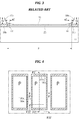
- FIG. 4 is a plan view illustrating an OLED display device according to an embodiment of the present invention.
- the OLED display device of the embodiment includes a plurality of pixel regions P, a first bank 130a and 130b in a boundary region separating the pixel regions P and located at a boundary portion of each pixel region P, and a second bank 150a and 150b in the boundary region not covering (e.g., exposing) edges of the first bank 130a and 130b and located on the first bank 130a and 130b.
- the edges of the first bank 130a and 130b not covered by the second bank 150a and 150b may be covered by a different layer, such as an organic light emitting layer as described below.
- the first bank 130a and 130b and second bank 150a and 150b may be located around a perimeter of the pixel region P.
- the first bank 130a and 130b is divided into a first portion 130a (e.g., a long edge portion) along a long side of the pixel region P and a second portion 130b (e.g., a short edge portion) along a short side of the pixel region P, and the second bank 150a and 150b is divided into a third portion 150a (e.g., a long edge portion) along the long side of the pixel region P and a fourth portion 150b (e.g., a short edge portion) along the short side of the pixel region P.
- a first portion 130a e.g., a long edge portion
- second portion 130b e.g., a short edge portion
- a width of the edge of the second portion 130b is greater than that of the first portion 130a.
- FIG. 5 is a cross-sectional view taken along a line V-V of FIG. 4
- FIG. 6 is a cross-sectional view taken along a line VI-VI of FIG. 4
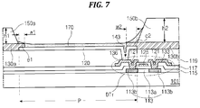
- FIG. 7 is a cross-sectional view taken along a line VII-VII of FIG. 4
- FIG. 5 is a cross-sectional view of the pixel region P and the boundary portion thereof along a minor axis of the pixel region
- FIG. 6 is a cross-sectional view of the pixel region P and the boundary portion thereof along a major axis of the pixel region
- FIG. 7 is a cross-sectional view of the pixel region P and the boundary portion thereof with a driving thin film transistor.
- the OLED display device of the embodiment includes a first electrode 120 on or over the substrate 101 in the pixel region P and in a boundary region separating the pixel regions P, the first bank 130a and 130b covering edges of the first electrode 120 in the pixel region P and on the substrate 101 in a boundary region surrounding the pixel region P, the second bank 150a and 150b on a portion of the first bank 130a and 130b in the boundary region, and an organic light emitting layer 170 on the first electrode 120 and on the first bank 130a and 130b in the pixel region and on at least a portion of the second bank in the boundary region.
- the first bank 130a and 130b is arranged to cover edges of the first electrode 120, and the second bank 150a and 150b is arranged to not cover the edges e1 and e2 of the first bank 130a and 130b (which may be covered by a different layer such as the organic light emitting layer 170).
- a width w1 of the edge e1 of the first portion 130a is different from a width w2 of the edge e2 of the second portion 130b.
- the width w2 of the edge e2 of the second portion 130b is greater than the width w1 of the edge e1 of the first portion 130a.
- the width w2 of the edge e2 of the second portion 130b may be about 7.5um to about 10um, and the width w1 of the edge e1 of the first portion 130b may be about 5um.
- the width w2 of the edge e2 of the second portion 130b may be about 6um to about 8um, and the width w1 of the edge e1 of the first portion 130b may be about 4um.
- the width w2 of the edge e2 of the second portion 130b may be about 4.5um to about 6um, and the width w1 of the edge e1 of the first portion 130b may be about 3um.
- the width w2 may be in the range of 1.5-2 times the width w1.
- a height h1 of the third portion 150a is different from a height h2 of the fourth portion 150b.
- the height h2 of the fourth portion 150b is greater than the height h1 of the third portion 150a.
- the height h2 of the fourth portion 150b may be about 1.5um to 2um, and the height h1 of the third portion 150a may be about 1um. In other example, the height h2 of the fourth portion 150b may be about 2.5um to 3um, and the height h1 of the third portion 150a may be about 2um. Thus, for example, the height h2 may be in the range of 1.25-2 times the height h1. Further, in an embodiment, the height h2 of the fourth portion 150b may be higher than the height h1 of the third portion 150a at least by 0.5um, and the height of h2 of the fourth portion 150b may be 3um or less.
- the heights h1 and h2 of the second bank 150a and 150b maybe formed differently.
- the second bank 150a and 150b having the different heights h1 and h2 can be formed, and thus production process can be simplified.
- the first electrode 120 may be made of a transparent conductive material, for example, indium-tin-oxide (ITO) or indium-zinc-oxide (IZO), having a relatively greater work function to function as an anode.
- ITO indium-tin-oxide
- IZO indium-zinc-oxide
- the first bank 130a and 130b may be made of an inorganic material, for example, silicon oxide (SiO2) or silicon nitride (SiNx), having a hydrophilicity.
- the second bank 150a and 150b may be made of an organic material, for example, polyacryl, polyimide, polyamide (PA), benzocyclobutene (BCB), or phenol resin, having a hydrophobicity.
- the OLED display device further includes the driving thin film transistor DTr located between the substrate 101 and the first electrode 120 and connected to the first electrode 120.
- the detailed structure of the driving thin film transistor DTr is explained with reference to FIG. 7 .
- a semiconductor layer 113 is located on the substrate 101 and includes a first region 113a made of intrinsic polysilicon, and a second region 113b located at each of both sides of the first region 113a and doped with highly concentrated impurities.
- a gate insulating layer 115 is located entirely on the substrate 101 and covers the semiconductor layer 113.
- a gate electrode 125 is located on the gate insulating layer 115 corresponding to the first region 113a.
- An inter-layered insulating layer 117 covers the gate electrode 125 and is entirely on the substrate 101.
- a semiconductor contact hole 121 exposing each second region 113b is formed in the gate insulating layer 115 and the inter-layered insulating layer 117.
- Source and drain electrodes 133 and 136 are located on the inter-layered insulating layer 117, are connected to the respective second regions 113b through the respective semiconductor contact holes 121, and are spaced apart from each other.
- the source and drain electrodes 133 and 136, the semiconductor layer 113, the gate electrode 125 form the driving thin film transistor DTr.
- a passivation layer 119 is located on the driving thin film transistor DTr over the entire substrate 101, and has a planarization property.
- a drain contact hole 143 exposing the drain electrode 136 is formed in the passivation layer 119.
- the drain electrode 136 is connected to the first electrode 120 through the drain contact hole 143.
- the organic light emitting layer 170 is located on the first electrode 120.
- a second electrode (not shown) is located on the organic light emitting layer 170 and the second bank 150a and 150b.
- the organic light emitting layer 170 is laminated using a soluble process such as an inkjet printing method, a nozzle printing method or the like.
- the organic light emitting layer 170 is formed by dropping an organic light emitting material solution on the first electrode 120 and then drying the organic light emitting material solution.
- a phenomenon occurs that a thickness of an edge portion of the organic light emitting layer 170 is greater than a thickness of a center portion of the organic light emitting layer 170 in the drying process. This phenomenon is referred to as a pile-up phenomenon.
- the dropped organic light emitting material solution contacts top surfaces of the edges e1 and e2 of the first bank 130a and 130b.
- the first bank 130a and 130b is made of an hydrophilic inorganic material, the first bank 130a and 130b has a surface energy greater than that of the second bank 150a and 150b, and a surface tension of the organic light emitting material solution at the top surfaces of the edges e1 and e2 of the first bank 130a and 130b is reduced.
- the pile-up phenomenon is induced from the top surfaces of the edges e1 and e2 of the first bank 130a and 130b to side walls of the second bank 150a and 150b.
- the width w2 of the edge e2 of the second portion 130b along the short side of the pixel region P is greater that the width w1 of the edge e1 of the first portion 130a along the long side of the pixel region P.
- the area at the edge e2 of the second portion 130b is wider than the area at the edge d1 of the first portion 130a.
- the height h2 of the fourth portion 150b along the short side of the pixel region P is greater than the height h1 of the third portion 150a along the long side of the pixel region P.
- the pile-up phenomenon at the side wall of the fourth portion 150b occurs relatively more while the pile-up phenomenon at the side wall of the third portion 150a occurs relatively less.
- an average height of the organic light emitting layer along its short edge portions on the second bank is greater than an average height of the organic light emitting layer along the long edge portions on the second bank.
- a width of the organic light emitting layer along its short edge portions over the first bank is greater than a width of the organic light emitting layer along its long edge portions over the first bank.
- Having greater pile-up phenomenon along the short edge portions beneficially acts to stretch the organic light emitting material and improves a uniformity of thickness of the display region across the pixel region P and results in the reduced pile-up along the long edge portions which forms part of the viewable display. Furthermore, the increased pile-up phenomenon along the short edge does not significantly affect the viewable display area because the area above the driving thin film transistor DTr along the short edge is not used for display or represents a less significant portion of the display, in one embodiment.
- the OLED display device of the embodiment can prevent a non-uniformity of brightness caused by reduction of a uniformity of thickness, and can improve light emission efficiency and lifetime of an organic light emitting diode.
- the driving thin film transistor DTr is arranged below the second portion 130b and the fourth portion 150b along the short side of the pixel region P.
- the driving thin film transistor DTr is arranged at the boundary portion of the lower side of the pixel region P.
- the driving thin film transistor DTr may be arranged at the boundary portion of the upper side of the pixel region P.
- at least a portion of the driving thin film transistor DTr is under the edge of the first bank 130b along either one of the short sides in the pixel region P.
- the driving thin film transistor DTr is arranged below the second portion 130b and the fourth portion 150b along the short side of the pixel region P where the pile-up phenomenon occurs relatively more, an aperture ratio of the OLED display device can be improved.
- the aperture ratio of the OLED display device can be further improved.
- the OLED display device is configured with the width w2 of the edge e2 of the second portion 130b being greater than the width w1 of the edge e1 of the first portion 130a and the height h2 of the fourth portion 150b being greater than the height h1 of the third portion 150a.
- the OLED can be configured with either, but not necessarily both, the width w2 of the edge e2 of the second portion 130b being greater than the width w1 of the edge e1 of the first portion 130a or the height h2 of the fourth portion 150b being greater than the height h1 of the third portion 150a, and this configuration can improve a uniformity of thickness sufficiently.
- the widths w1 and w2 of the first bank and/or the heights h1 and h2 of the second bank can be dimensioned to improve a uniformity of thickness.
Landscapes
- Engineering & Computer Science (AREA)
- Manufacturing & Machinery (AREA)
- Microelectronics & Electronic Packaging (AREA)
- Physics & Mathematics (AREA)
- Geometry (AREA)
- Electroluminescent Light Sources (AREA)
Abstract
Description
- The present application claims the priority benefit of Korean Patent Application No.
10-2015-0093651 - The present invention relates to an organic light emitting diode (OLED) display device. In particular, the present invention relates to an OLED display device that has improved uniformity of thickness of an organic light emitting layer.
- Recently, flat display devices, such as a plasma display panel (PDP), a liquid crystal display (LCD) device, and an organic light emitting diode (OLED) display device, have been researched.
- Among the flat display devices, the OLED display device is a self-luminescent device and can have a thin profile because the OLED display device does not need a backlight used for the LCD device.
- Further, compared with the LCD device, the OLED display device has advantages of excellent viewing angle and contrast ratio, low power consumption, operation in low DC voltage, fast response speed, being strong to an external impact because of its solid internal components, and wide operating temperature range.
- Particularly, since processes of manufacturing the OLED display device are simple, production cost of the OLED display device can be reduced more that that of the LCD device.
-
FIG. 1 is a plan view illustrating an OLED display device according to the related art. - As shown in
FIG. 1 , the related art OLED display device includes a plurality of pixel regions P, afirst bank second bank first bank first bank - The
first bank first portion 30a along a long side of the pixel region P and asecond portion 30b along a short side of the pixel region P, and thesecond bank third portion 50a along the long side of the pixel region P and afourth portion 50b along the short side of the pixel region P. - A width of the edge of the
first portion 30a is equal to that of thesecond portion 30b. -
FIG. 2 is a cross-sectional view taken along a line II-II ofFIG. 1 , andFIG. 3 is a cross-sectional view taken along a line III-III ofFIG. 1 . In more detail,FIG. 2 is a cross-sectional view of the pixel region P and the boundary portion thereof along a minor axis of the pixel region, andFIG. 3 is a cross-sectional view of the pixel region P and the boundary portion thereof along a major axis of the pixel region. - As shown in
FIGs. 2 and3 , the related art OLED display device includes afirst electrode 20 in the pixel region P on asubstrate 11, thefirst bank substrate 11, thesecond bank first bank light emitting layer 70 on thefirst electrode 20. - The
first bank first electrode 20, and thesecond bank first bank - A width w1 of an edge e1 of the
first portion 30a is equal to a width w2 of an edge e2 of thesecond portion 30b. - For example, the width w1 of the edge e1 of the
first portion 30a and the width w2 of the edge e2 of thesecond portion 30b may be equally 1um to 10um. - Further, a height h1 of the
third portion 50a is equal to a height h2 of thefourth portion 50b. - For example, the height h1 of the
third portion 50a and the height h2 of thefourth portion 50b maybe equally 1 micrometre (um) to 10um. - The
first electrode 20 may be made of a transparent conductive material having a relatively greater work function to function as an anode. Thefirst bank second bank - The OLED display device further includes a driving thin film transistor DTr located between the
substrate 11 and thefirst electrode 20 and connected to thefirst electrode 20. - The organic
light emitting layer 70 is laminated using a soluble process such as an inkjet printing method, a nozzle printing method or the like. - In detail, the organic
light emitting layer 70 is formed by dropping an organic light emitting material solution on thefirst electrode 20 and then drying the organic light emitting material solution. - A phenomenon occurs that a thickness of an edge portion of the organic
light emitting layer 70 is greater than a thickness of a center portion of the organiclight emitting layer 70 in the drying process. This phenomenon is referred to as a pile-up phenomenon. - In this case, since the edges e1 and e2 of the
first bank second bank first bank - Further, since the
first bank first bank second bank first bank - Accordingly, the pile-up phenomenon is induced from the top surfaces of the edges e1 and e2 of the
first bank second bank - Thus, the pile-up phenomenon at the boundary portion of a display region out of the pixel region P the can be relieved to some extent.
- In other words, a uniformity of thickness of the display region of the pixel region P can be improved to some extent.
- However, since the pile-up phenomenon at the boundary portion is not completely improved, a non-uniformity of brightness still occurs due to reduction of a uniformity of thickness of the organic
light emitting layer 70 and light emission efficiency and lifetime of the OLED display device are reduced. - Further, since the dual banks of the
first bank second bank - Accordingly, the present invention is directed to an OLED display device that substantially obviates one or more of the problems due to limitations and disadvantages of the related art.
- An object of the present invention is to improve a uniformity of thickness of an organic light emitting layer and a non-uniformity of brightness.
- Additional features and advantages of the disclosure will be set forth in the description which follows, and in part will be apparent from the description, or may be learned by practice of the disclosure. The advantages of the disclosure will be realized and attained by the structure particularly pointed out in the written description and claims as well as the appended drawings.
- Aspects of an invention are defined in the appended independent claims.
- To achieve these and other advantages, and in accordance with the purpose of the present invention, as embodied and broadly described herein, an organic light emitting diode (OLED) display device includes a pixel region and a boundary region outside the pixel region. The pixel region comprises an area having a short side and a long side. The pixel region comprises an array of pixels to emit light. The OLED display device includes a substrate in the pixel region and in the boundary region, a first electrode of a light emitting device in the pixel region over the substrate, a first bank covering edges of the first electrode in the pixel region and on the substrate in the boundary region, and a second bank on a portion of the first bank in the boundary region, wherein a width of an edge of the first bank along the short side of the pixel region is different from a width of an edge of the first bank along the long side of the pixel region.
- Also disclosed, an organic light emitting display (OLED) device includes a pixel region and a boundary region outside the pixel region. The pixel region comprises an area having a short dimension and a long dimension. The pixel region comprises an array of pixels to emit light. A substrate is in the pixel region and in the boundary region. An electrode is on the substrate in the pixel region. The electrode has long edge portions oriented along the long dimension of the pixel region and the electrode has short edge portions oriented along the short dimension of the pixel region. A first bank is on the substrate in the boundary region and on the long and the short edge portions of the electrode in the pixel region. A second bank is on the first bank in the boundary region. The second bank has long edge portions oriented along the long dimension of the pixel region and short edge portions oriented along the short dimension of the pixel region. An organic light emitting layer is on the electrode and on the first bank in the pixel region and on at least a portion of the second bank in the boundary region. An average height of short edge portions of the organic light emitting layer on the second bank is greater than an average height of long edge portions of the organic light emitting layer on the second bank.
- Also disclosed, a display device comprises a plurality of pixel regions each comprising an area having a short dimension and a long dimension. Each of the pixel regions comprises an array of pixels to emit light. A plurality of boundary regions separates the pixel regions. The boundary regions comprise a first bank and a second bank. The first bank comprises a hydrophilic material around a perimeter of the pixel region. The second bank comprises a hydrophobic material on a portion of the first bank around the perimeter of the pixel region. The second bank has long edge portions along the long dimension and short edge portions along the short dimension. A first height of the short edge portions of the second bank is greater than a second height of the long edge portions of the second bank.
- It is to be understood that both the foregoing general description and the following detailed description are exemplary and explanatory and are intended to provide further explanation of the invention as claimed.
- The accompanying drawings, which are included to provide a further understanding of the disclosure and are incorporated in and constitute a part of this specification, illustrate embodiments of the disclosure and together with the description serve to explain the principles of the disclosure. In the drawings:
-
FIG. 1 is a plan view illustrating an OLED display device according to the related art; -
FIG. 2 is a cross-sectional view taken along a line II-II ofFIG. 1 ; -
FIG. 3 is a cross-sectional view taken along a line III-III ofFIG. 1 ; -
FIG. 4 is a plan view illustrating an OLED display device according to an embodiment of the present invention; -
FIG. 5 is a cross-sectional view taken along a line V-V ofFIG. 4 ; -
FIG. 6 is a cross-sectional view taken along a line VI-VI ofFIG. 4 ; and -
FIG. 7 is a cross-sectional view taken along a line VII-VII ofFIG. 4 . - Reference will now be made in detail to embodiments, examples of which are illustrated in the accompanying drawings. The same or like reference numbers may be used throughout the drawings to refer to the same or like parts.
-
FIG. 4 is a plan view illustrating an OLED display device according to an embodiment of the present invention. - As shown in
FIG. 4 , the OLED display device of the embodiment includes a plurality of pixel regions P, afirst bank second bank first bank first bank first bank second bank first bank second bank - The
first bank first portion 130a (e.g., a long edge portion) along a long side of the pixel region P and asecond portion 130b (e.g., a short edge portion) along a short side of the pixel region P, and thesecond bank third portion 150a (e.g., a long edge portion) along the long side of the pixel region P and afourth portion 150b (e.g., a short edge portion) along the short side of the pixel region P. - A width of the edge of the
second portion 130b is greater than that of thefirst portion 130a. -
FIG. 5 is a cross-sectional view taken along a line V-V ofFIG. 4 ,FIG. 6 is a cross-sectional view taken along a line VI-VI ofFIG. 4 , andFIG. 7 is a cross-sectional view taken along a line VII-VII ofFIG. 4 . In more detail,FIG. 5 is a cross-sectional view of the pixel region P and the boundary portion thereof along a minor axis of the pixel region,FIG. 6 is a cross-sectional view of the pixel region P and the boundary portion thereof along a major axis of the pixel region, andFIG. 7 is a cross-sectional view of the pixel region P and the boundary portion thereof with a driving thin film transistor. - As shown in
FIGs. 5-7 , the OLED display device of the embodiment includes afirst electrode 120 on or over thesubstrate 101 in the pixel region P and in a boundary region separating the pixel regions P, thefirst bank first electrode 120 in the pixel region P and on thesubstrate 101 in a boundary region surrounding the pixel region P, thesecond bank first bank light emitting layer 170 on thefirst electrode 120 and on thefirst bank - The
first bank first electrode 120, and thesecond bank first bank - A width w1 of the edge e1 of the
first portion 130a is different from a width w2 of the edge e2 of thesecond portion 130b. - In detail, the width w2 of the edge e2 of the
second portion 130b is greater than the width w1 of the edge e1 of thefirst portion 130a. - For example, the width w2 of the edge e2 of the
second portion 130b may be about 7.5um to about 10um, and the width w1 of the edge e1 of thefirst portion 130b may be about 5um. In other example, the width w2 of the edge e2 of thesecond portion 130b may be about 6um to about 8um, and the width w1 of the edge e1 of thefirst portion 130b may be about 4um. In other example, the width w2 of the edge e2 of thesecond portion 130b may be about 4.5um to about 6um, and the width w1 of the edge e1 of thefirst portion 130b may be about 3um. Thus, in one embodiment, the width w2 may be in the range of 1.5-2 times the width w1. - Further, a height h1 of the
third portion 150a is different from a height h2 of thefourth portion 150b. - In detail, the height h2 of the
fourth portion 150b is greater than the height h1 of thethird portion 150a. - For example, the height h2 of the
fourth portion 150b may be about 1.5um to 2um, and the height h1 of thethird portion 150a may be about 1um. In other example, the height h2 of thefourth portion 150b may be about 2.5um to 3um, and the height h1 of thethird portion 150a may be about 2um. Thus, for example, the height h2 may be in the range of 1.25-2 times the height h1. Further, in an embodiment, the height h2 of thefourth portion 150b may be higher than the height h1 of thethird portion 150a at least by 0.5um, and the height of h2 of thefourth portion 150b may be 3um or less. - In this case, using a half-tone mask or the like including a blocking region, a semi-transmissive region and a transmissive region, the heights h1 and h2 of the
second bank - Accordingly, the
second bank - The
first electrode 120 may be made of a transparent conductive material, for example, indium-tin-oxide (ITO) or indium-zinc-oxide (IZO), having a relatively greater work function to function as an anode. - The
first bank second bank - The OLED display device further includes the driving thin film transistor DTr located between the
substrate 101 and thefirst electrode 120 and connected to thefirst electrode 120. - The detailed structure of the driving thin film transistor DTr is explained with reference to
FIG. 7 . - A
semiconductor layer 113 is located on thesubstrate 101 and includes afirst region 113a made of intrinsic polysilicon, and asecond region 113b located at each of both sides of thefirst region 113a and doped with highly concentrated impurities. - A
gate insulating layer 115 is located entirely on thesubstrate 101 and covers thesemiconductor layer 113. Agate electrode 125 is located on thegate insulating layer 115 corresponding to thefirst region 113a. An inter-layeredinsulating layer 117 covers thegate electrode 125 and is entirely on thesubstrate 101. - A
semiconductor contact hole 121 exposing eachsecond region 113b is formed in thegate insulating layer 115 and the inter-layeredinsulating layer 117. - Source and
drain electrodes insulating layer 117, are connected to the respectivesecond regions 113b through the respective semiconductor contact holes 121, and are spaced apart from each other. - The source and drain
electrodes semiconductor layer 113, thegate electrode 125 form the driving thin film transistor DTr. - A
passivation layer 119 is located on the driving thin film transistor DTr over theentire substrate 101, and has a planarization property. - A
drain contact hole 143 exposing thedrain electrode 136 is formed in thepassivation layer 119. Thedrain electrode 136 is connected to thefirst electrode 120 through thedrain contact hole 143. - The organic
light emitting layer 170 is located on thefirst electrode 120. A second electrode (not shown) is located on the organiclight emitting layer 170 and thesecond bank - The organic
light emitting layer 170 is laminated using a soluble process such as an inkjet printing method, a nozzle printing method or the like. - The organic
light emitting layer 170 is formed by dropping an organic light emitting material solution on thefirst electrode 120 and then drying the organic light emitting material solution. - A phenomenon occurs that a thickness of an edge portion of the organic
light emitting layer 170 is greater than a thickness of a center portion of the organiclight emitting layer 170 in the drying process. This phenomenon is referred to as a pile-up phenomenon. - In this case, since the edges e1 and e2 of the
first bank second bank first bank - Further, since the
first bank first bank second bank first bank - Accordingly, the pile-up phenomenon is induced from the top surfaces of the edges e1 and e2 of the
first bank second bank - Further, as shown in the drawings, the width w2 of the edge e2 of the
second portion 130b along the short side of the pixel region P is greater that the width w1 of the edge e1 of thefirst portion 130a along the long side of the pixel region P. - Accordingly, regarding areas that contact the dropped organic light emitting material solution, the area at the edge e2 of the
second portion 130b is wider than the area at the edge d1 of thefirst portion 130a. - Further, as shown in the drawings, the height h2 of the
fourth portion 150b along the short side of the pixel region P is greater than the height h1 of thethird portion 150a along the long side of the pixel region P. - Accordingly, in the drying process of the organic light emitting material solution, the pile-up phenomenon at the side wall of the
fourth portion 150b occurs relatively more while the pile-up phenomenon at the side wall of thethird portion 150a occurs relatively less. Thus, an average height of the organic light emitting layer along its short edge portions on the second bank is greater than an average height of the organic light emitting layer along the long edge portions on the second bank. Furthermore, due to the difference in pile-up phenomenon, a width of the organic light emitting layer along its short edge portions over the first bank is greater than a width of the organic light emitting layer along its long edge portions over the first bank. - Having greater pile-up phenomenon along the short edge portions beneficially acts to stretch the organic light emitting material and improves a uniformity of thickness of the display region across the pixel region P and results in the reduced pile-up along the long edge portions which forms part of the viewable display. Furthermore, the increased pile-up phenomenon along the short edge does not significantly affect the viewable display area because the area above the driving thin film transistor DTr along the short edge is not used for display or represents a less significant portion of the display, in one embodiment.
- Thus, the OLED display device of the embodiment can prevent a non-uniformity of brightness caused by reduction of a uniformity of thickness, and can improve light emission efficiency and lifetime of an organic light emitting diode.
- Further, the driving thin film transistor DTr is arranged below the
second portion 130b and thefourth portion 150b along the short side of the pixel region P. - In the drawings, it is shown that the driving thin film transistor DTr is arranged at the boundary portion of the lower side of the pixel region P. Alternatively, the driving thin film transistor DTr may be arranged at the boundary portion of the upper side of the pixel region P. Thus, for example, at least a portion of the driving thin film transistor DTr is under the edge of the
first bank 130b along either one of the short sides in the pixel region P. - Accordingly, since the driving thin film transistor DTr is arranged below the
second portion 130b and thefourth portion 150b along the short side of the pixel region P where the pile-up phenomenon occurs relatively more, an aperture ratio of the OLED display device can be improved. - Further, even though the dual banks of the
first bank second bank second portions - In the above embodiment, it is described that, in order to improve a uniformity of thickness, the OLED display device is configured with the width w2 of the edge e2 of the
second portion 130b being greater than the width w1 of the edge e1 of thefirst portion 130a and the height h2 of thefourth portion 150b being greater than the height h1 of thethird portion 150a. In another embodiment, the OLED can be configured with either, but not necessarily both, the width w2 of the edge e2 of thesecond portion 130b being greater than the width w1 of the edge e1 of thefirst portion 130a or the height h2 of thefourth portion 150b being greater than the height h1 of thethird portion 150a, and this configuration can improve a uniformity of thickness sufficiently. In other words, the widths w1 and w2 of the first bank and/or the heights h1 and h2 of the second bank can be dimensioned to improve a uniformity of thickness. - It will be apparent to those skilled in the art that various modifications and variations can be made in a display device of the present invention without departing from the scope of the disclosure. Thus, it is intended that the present invention covers the modifications and variations of this disclosure provided they come within the scope of the appended claims and their equivalents.
- Also disclosed is:
- Clause 1. An organic light emitting diode (OLED) display device including a pixel region and a boundary region outside the pixel region, the pixel region comprising an area having a short side and a long side, the pixel region comprising an array of pixels to emit light, the OLED display device comprising:
- a substrate in the pixel region and in the boundary region;
- a first electrode of a light emitting device in the pixel region over the substrate;
- a first bank covering edges of the first electrode in the pixel region and on the substrate in the boundary region, wherein a width of an edge of the first bank along the short side of the pixel region is different from a width of an edge of the first bank along the long side of the pixel region; and
- a second bank on a portion of the first bank in the boundary region.
- Clause 2. The OLED display device of clause 1, wherein a height of the second bank along the short side of the pixel region is different from a height of the second bank along the long side of the pixel region.
- Clause 3. The OLED display device of clause 1, wherein the width of the edge of the first bank along the short side of the pixel region is greater than the width of the edge of the first bank along the long side of the pixel region.
- Clause 4. The OLED display device of clause 1, wherein a height of the second bank along the short side of the pixel region is greater than a height of the second bank along the long side of the pixel region.
- Clause 5. The OLED display device of clause 4, wherein the first bank comprises a hydrophilic inorganic material, and the second bank comprises a hydrophobic organic material.
- Clause 6. The OLED display device of clause 1, further comprising a driving thin film transistor between the substrate and the first electrode and connected to the first electrode.
- Clause 7. The OLED display device of clause 6, wherein at least a portion of the driving thin film transistor is under the edge of the first bank along the short side of the pixel region.
- Clause 8. The OLED display device of clause 1, further comprising:
- an organic light emitting layer on the first electrode in the pixel region; and
- a second electrode on the organic light emitting layer and the second bank.
- Clause 9. The OLED display device of clause 8, wherein the organic light emitting layer is laminated using a soluble process.
- Clause 10. The OLED display device of clause 8, wherein the width of the edge of the first bank along the short side of the pixel region and the width of the edge of the first bank along the long side of the pixel region are dimensioned such that an average height of short edge portions of the organic light emitting layer on the second bank is greater than an average height of long edge portions of the organic light emitting layer on the second bank.
-
Clause 11. The OLED display device of clause 8, wherein a height of the second bank along the short side of the pixel region and a height of the second bank along the long side of the pixel region are dimensioned such that an average height of short edge portions of the organic light emitting layer on the second bank is greater than an average height of long edge portions of the organic light emitting layer on the second bank. - Clause 12. An organic light emitting diode (OLED) display device including a pixel region and a boundary region outside the pixel region, the pixel region comprising an area having a short dimension and a long dimension, the pixel region comprising an array of pixels to emit light, the OLED display device comprising:
- a substrate in the pixel region and in the boundary region;
- an electrode on the substrate in the pixel region, the electrode having long edge portions oriented along the long dimension of the pixel region and the electrode having short edge portions oriented along the short dimension of the pixel region;
- a first bank on the substrate in the boundary region and on the long and the short edge portions of the electrode in the pixel region;
- a second bank on the first bank in the boundary region, the second bank having long edge portions oriented along the long dimension of the pixel region and short edge portions oriented along the short dimension of the pixel region;
- an organic light emitting layer on the electrode and on the first bank in the pixel region and on at least a portion of the second bank in the boundary region, wherein an average height of short edge portions of the organic light emitting layer on the second bank is greater than an average height of long edge portions of the organic light emitting layer on the second bank.
- Clause 13. The OLED display device of clause 12, wherein a width of short edge portions of the organic light emitting layer over the first bank along the short dimension is different than a width of long edge portions of the organic light emitting layer over the first bank along the long dimension.
- Clause 14. The OLED display device of clause 13, wherein the width of the short edge portions of the organic light emitting layer over the first bank along the short dimension is greater than the width of the long edge portions of the organic light emitting layer over the first bank along the long dimension.
- Clause 15. The OLED display device of clause 12, wherein widths of short edge portions of the first bank on the short edge portions of the electrode are greater than widths of long edge portions of the first bank on the short edge portions of the electrode.
- Clause 16. The OLED display device of clause 15, wherein the widths of the short edge portions of the first bank are in a range of approximately 1.5 - 2 times the widths of the long edge portions of the first bank.
- Clause 17. The OLED display device of clause 12, wherein heights of the short edge portions of the second bank are greater than heights of the long edge portions of the second bank.
- Clause 18. The OLED display device of clause 17, wherein the heights of the short edge portions of the second bank are in a range of approximately 1.25-2 times the heights of the long edge portions of the second bank.
- Clause 19. The OLED display device of clause 17, wherein the heights of the short edge portions of the second bank are in a range of about 3um or less and are at least 0.5um greater than the heights of the long edge portions of the second bank.
-
Clause 20. The OLED display device of clause 12, wherein the first bank comprises a hydrophilic inorganic material, and the second bank comprises a hydrophobic organic material. - Clause 21. The OLED display device of clause 12, wherein widths of short edge portions of the first bank on the short edge portions of the electrode and widths of long edge portions of the first bank on the long edge portions of the electrode are dimensioned such that the average height of the short edge portions of the organic light emitting layer on the second bank is greater than the average height of the long edge portions of the organic light emitting layer on the second bank.
- Clause 22. The OLED display device of clause 12, wherein heights of the short edge portions of the second bank and heights of the long edge portions of the second bank are dimensioned such that the average height of the short edge portions of the organic light emitting layer on the second bank is greater than the average height of the long edge portions of the organic light emitting layer on the second bank.
- Clause 23. A display device comprising:
- a plurality of pixel regions each comprising an area having a short dimension and a long dimension, each of the pixel regions comprising an array of pixels to emit light;
- a plurality of boundary regions separating the pixel regions, the boundary regions comprising:
- a first bank comprising a hydrophilic material around a perimeter of the pixel region;
- a second bank comprising a hydrophobic material on a portion of the first bank around the perimeter of the pixel region, the second bank having long edge portions along the long dimension and short edge portions along the short dimension, wherein a first height of the short edge portions of the second bank is greater than a second height of the long edge portions of the second bank.
- Clause 24. The display device of clause 23, wherein the first height is in a range of approximately 1.25 to 2 times the second height.
- Clause 25. The display device of clause 23, wherein the first height is in a range of about 3um or less and is at least 0.5um greater than the second height.
- Clause 26. The display device of clause 23, wherein the first bank comprises an inorganic material and wherein the second bank comprises an organic material.
- Clause 27. The display device of clause 23, further comprising an organic light emitting layer on the first bank in the pixel region and on at least a portion of the second bank in the boundary region, wherein the first height and the second height are dimensioned such that an average height of short edge portions of the organic light emitting layer on the second bank is greater than an average height of long edge portions of the organic light emitting layer on the second bank.
- Clause 28. The display device of clause 23, further comprising an organic light emitting layer on the first bank in the pixel region and on at least a portion of the second bank in the boundary region, wherein a width of short edge portions of the first bank along the short dimension and a width of long edge portions of the first bank along the long dimension are dimensioned such that an average height of short edge portions of the organic light emitting layer on the second bank is greater than an average height of long edge portions of the organic light emitting layer on the second bank.
Claims (15)
- An organic light emitting diode "OLED" display device comprising an array of pixels to emit light, the OLED display device comprising:a substrate (101) defining a pixel region and a boundary region outside the pixel region, the pixel region comprising an area having a short side and a long side;a first electrode (120) in the pixel region;a first bank (130a, 130b) overlapping edges of the first electrode in the pixel region and on the substrate in the boundary region, wherein a width (w2) of an edge (e2) of the first bank along the short side of the pixel region is different from a width (w1) of an edge (e1) of the first bank along the long side of the pixel region, wherein the edge of the bank is the portion of the bank in the pixel region; anda second bank (150a,150b) on a portion of the first bank in the boundary region.
- The OLED display device of claim 1, wherein the pixel region comprises the array of pixels.
- The OLED display device of claim 1 or claim 2, wherein the first bank is around a perimeter of the pixel region and the second bank is around the perimeter of the pixel region.
- The OLED display device of any preceding claim, wherein a height (h2) of the second bank along the short side of the pixel region is different from a height (h1) of the second bank along the long side of the pixel region.
- The OLED display device of any preceding claim, wherein the width of the edge of the first bank along the short side of the pixel region is greater than the width of the edge of the first bank along the long side of the pixel region.
- The OLED display device of any preceding claim, wherein a height of the second bank along the short side of the pixel region is greater than a height of the second bank along the long side of the pixel region.
- The OLED display device of any preceding claim, wherein the first bank comprises a hydrophilic inorganic material, and the second bank comprises a hydrophobic organic material.
- The OLED display device of any preceding claim, further comprising a driving thin film transistor (DTr) between the substrate and the first electrode and connected to the first electrode.
- The OLED display device of claim 8, wherein at least a portion of the driving thin film transistor is under the edge of the first bank along the short side of the pixel region.
- The OLED display device of any preceding claim, further comprising:an organic light emitting layer (170) on the first electrode in the pixel region.
- The OLED display device of claim 10, further comprising a second electrode on the organic light emitting layer and the second bank.
- The OLED display device of claim 10 or claim 11, wherein the organic light emitting layer is laminated using a soluble process.
- The OLED display device of claims 10 to 12, wherein the width of the edge of the first bank along the short side of the pixel region and the width of the edge of the first bank along the long side of the pixel region are dimensioned such that an average height of short edge portions of the organic light emitting layer on the second bank are greater than an average height of long edge portions of the organic light emitting layer on the second bank.
- The OLED display device of any of claims 10 to 13, wherein a height of the second bank along the short side of the pixel region and a height of the second bank along the long side of the pixel region are dimensioned such that an average height of short edge portions of the organic light emitting layer on the second bank is greater than an average height of long edge portions of the organic light emitting layer on the second bank.
- The OLED display device of any preceding claim, wherein the widths of the short edge portions of the first bank are in a range of approximately 1.5 - 2 times the widths of the long edge portions of the first bank.
Priority Applications (2)
| Application Number | Priority Date | Filing Date | Title |
|---|---|---|---|
| EP18181556.4A EP3428969B1 (en) | 2015-06-30 | 2016-06-30 | Organic light emitting diode display device |
| PL16177099T PL3113228T3 (en) | 2015-06-30 | 2016-06-30 | Display device with organic light-emitting diodes |
Applications Claiming Priority (1)
| Application Number | Priority Date | Filing Date | Title |
|---|---|---|---|
| KR1020150093651A KR102457536B1 (en) | 2015-06-30 | 2015-06-30 | Organic light emitting display device |
Related Child Applications (1)
| Application Number | Title | Priority Date | Filing Date |
|---|---|---|---|
| EP18181556.4A Division EP3428969B1 (en) | 2015-06-30 | 2016-06-30 | Organic light emitting diode display device |
Publications (2)
| Publication Number | Publication Date |
|---|---|
| EP3113228A1 true EP3113228A1 (en) | 2017-01-04 |
| EP3113228B1 EP3113228B1 (en) | 2018-07-04 |
Family
ID=56321794
Family Applications (2)
| Application Number | Title | Priority Date | Filing Date |
|---|---|---|---|
| EP18181556.4A Active EP3428969B1 (en) | 2015-06-30 | 2016-06-30 | Organic light emitting diode display device |
| EP16177099.5A Active EP3113228B1 (en) | 2015-06-30 | 2016-06-30 | Organic light emitting diode display device |
Family Applications Before (1)
| Application Number | Title | Priority Date | Filing Date |
|---|---|---|---|
| EP18181556.4A Active EP3428969B1 (en) | 2015-06-30 | 2016-06-30 | Organic light emitting diode display device |
Country Status (5)
| Country | Link |
|---|---|
| US (2) | US9947732B2 (en) |
| EP (2) | EP3428969B1 (en) |
| KR (1) | KR102457536B1 (en) |
| CN (1) | CN106328675B (en) |
| PL (1) | PL3113228T3 (en) |
Cited By (1)
| Publication number | Priority date | Publication date | Assignee | Title |
|---|---|---|---|---|
| EP3706173A4 (en) * | 2017-10-31 | 2021-09-08 | BOE Technology Group Co., Ltd. | DISPLAY SUBSTRATE AND ITS MANUFACTURING PROCESS, AND DISPLAY SCREEN |
Families Citing this family (18)
| Publication number | Priority date | Publication date | Assignee | Title |
|---|---|---|---|---|
| CN107689427B (en) * | 2017-02-09 | 2019-07-19 | 广东聚华印刷显示技术有限公司 | OLED device and preparation method thereof |
| CN109801939B (en) | 2017-11-17 | 2021-11-16 | 京东方科技集团股份有限公司 | Display substrate, manufacturing method thereof and display device |
| CN108010946B (en) * | 2017-11-27 | 2022-02-25 | 京东方科技集团股份有限公司 | Pixel defining layer, array substrate and display device |
| CN109860223B (en) | 2017-11-30 | 2021-01-22 | 京东方科技集团股份有限公司 | Pixel defining layer, display substrate, display device and ink-jet printing method |
| KR102513383B1 (en) * | 2017-12-05 | 2023-03-22 | 엘지디스플레이 주식회사 | Electroluminescent Display Device |
| CN108010953B (en) * | 2017-12-06 | 2020-06-26 | 京东方科技集团股份有限公司 | Organic light-emitting display backplane, preparation method thereof, and display device |
| KR102577043B1 (en) * | 2017-12-11 | 2023-09-08 | 엘지디스플레이 주식회사 | Electroluminescent display device |
| KR102657529B1 (en) * | 2018-11-02 | 2024-04-12 | 엘지디스플레이 주식회사 | Organic light-emitting display device |
| CN109546004B (en) * | 2018-12-05 | 2020-06-30 | 武汉华星光电半导体显示技术有限公司 | Light-emitting panel, manufacturing method of light-emitting panel and display device |
| KR20200071429A (en) | 2018-12-11 | 2020-06-19 | 엘지디스플레이 주식회사 | Organic light emitting display device and metho of fabricating thereof |
| KR102794930B1 (en) * | 2018-12-26 | 2025-04-10 | 엘지디스플레이 주식회사 | Organic light emitting display device |
| KR102803958B1 (en) * | 2018-12-26 | 2025-05-07 | 엘지디스플레이 주식회사 | Organic light emitting display device |
| CN109860422B (en) * | 2019-01-31 | 2021-06-04 | 武汉天马微电子有限公司 | Display panels and display devices |
| CN110071157B (en) * | 2019-04-28 | 2021-01-22 | 京东方科技集团股份有限公司 | Pixel defining layer and method for fabricating the same, array substrate, display panel and device |
| JP7330779B2 (en) * | 2019-06-27 | 2023-08-22 | 住友化学株式会社 | Organic EL device and its manufacturing method |
| KR102922937B1 (en) * | 2019-12-31 | 2026-02-03 | 엘지디스플레이 주식회사 | Organic light emitting display device |
| KR102952328B1 (en) * | 2020-12-31 | 2026-04-14 | 엘지디스플레이 주식회사 | Display panel and manufacturing method thereof |
| CN119012744B (en) * | 2024-07-22 | 2025-12-09 | 合肥维信诺科技有限公司 | Display panel and display device |
Citations (5)
| Publication number | Priority date | Publication date | Assignee | Title |
|---|---|---|---|---|
| US20050116632A1 (en) * | 2003-11-27 | 2005-06-02 | Seiko Epson Corporation | Electro-optic device, semiconductor device, electro-optic device substrate, manufacturing methods thereof, and electronic apparatus |
| US20070035242A1 (en) * | 2005-06-29 | 2007-02-15 | Dong-Won Lee | Display device and manufacturing method |
| US20090026467A1 (en) * | 2007-07-23 | 2009-01-29 | Seiko Epson Corporation | Electrooptical device, electronic apparatus, and method for producing electrooptical device |
| US20140145158A1 (en) * | 2012-11-26 | 2014-05-29 | Lg Display Co., Ltd. | Organic light emitting diode display device and method of fabricating the same |
| US20150001486A1 (en) * | 2013-06-28 | 2015-01-01 | Lg Display Co., Ltd. | Organic light emitting diode display device and method of fabricating the same |
Family Cites Families (12)
| Publication number | Priority date | Publication date | Assignee | Title |
|---|---|---|---|---|
| US7230592B2 (en) * | 2002-03-04 | 2007-06-12 | Hitachi, Ltd. | Organic electroluminescent light emitting display device |
| JP4161956B2 (en) * | 2004-05-27 | 2008-10-08 | セイコーエプソン株式会社 | Color filter substrate manufacturing method, electro-optical device manufacturing method, electro-optical device, and electronic apparatus |
| JP4507978B2 (en) * | 2005-05-16 | 2010-07-21 | セイコーエプソン株式会社 | Method for forming a film pattern |
| JP2007234232A (en) * | 2006-02-27 | 2007-09-13 | Hitachi Displays Ltd | Image display device |
| JP2009259457A (en) * | 2008-04-14 | 2009-11-05 | Seiko Epson Corp | Organic electroluminescent device and method of manufacturing the same, and electronic apparatus |
| JP5735527B2 (en) * | 2010-10-15 | 2015-06-17 | 株式会社Joled | ORGANIC LIGHT EMITTING PANEL, ITS MANUFACTURING METHOD, AND ORGANIC DISPLAY DEVICE |
| KR101904012B1 (en) * | 2011-09-30 | 2018-10-04 | 엘지디스플레이 주식회사 | Organic light emitting display device and method for fabricating the same |
| KR101941178B1 (en) * | 2012-09-28 | 2019-01-23 | 삼성디스플레이 주식회사 | Organic light emitting display device and method of manufacturing an organic light emitting display device |
| KR102015846B1 (en) * | 2012-11-26 | 2019-08-29 | 엘지디스플레이 주식회사 | Organic electro-luminescent device |
| KR20140067645A (en) * | 2012-11-27 | 2014-06-05 | 엘지디스플레이 주식회사 | Organic electro-luminescent device and method of fabricating the same |
| US9887253B2 (en) * | 2014-01-27 | 2018-02-06 | Japan Display Inc. | Light emitting element display device |
| JP6535977B2 (en) * | 2014-03-27 | 2019-07-03 | セイコーエプソン株式会社 | Method of manufacturing light emitting device |
-
2015
- 2015-06-30 KR KR1020150093651A patent/KR102457536B1/en active Active
-
2016
- 2016-06-15 US US15/183,727 patent/US9947732B2/en active Active
- 2016-06-24 CN CN201610474133.1A patent/CN106328675B/en active Active
- 2016-06-30 PL PL16177099T patent/PL3113228T3/en unknown
- 2016-06-30 EP EP18181556.4A patent/EP3428969B1/en active Active
- 2016-06-30 EP EP16177099.5A patent/EP3113228B1/en active Active
-
2018
- 2018-03-20 US US15/927,038 patent/US10297650B2/en active Active
Patent Citations (5)
| Publication number | Priority date | Publication date | Assignee | Title |
|---|---|---|---|---|
| US20050116632A1 (en) * | 2003-11-27 | 2005-06-02 | Seiko Epson Corporation | Electro-optic device, semiconductor device, electro-optic device substrate, manufacturing methods thereof, and electronic apparatus |
| US20070035242A1 (en) * | 2005-06-29 | 2007-02-15 | Dong-Won Lee | Display device and manufacturing method |
| US20090026467A1 (en) * | 2007-07-23 | 2009-01-29 | Seiko Epson Corporation | Electrooptical device, electronic apparatus, and method for producing electrooptical device |
| US20140145158A1 (en) * | 2012-11-26 | 2014-05-29 | Lg Display Co., Ltd. | Organic light emitting diode display device and method of fabricating the same |
| US20150001486A1 (en) * | 2013-06-28 | 2015-01-01 | Lg Display Co., Ltd. | Organic light emitting diode display device and method of fabricating the same |
Cited By (3)
| Publication number | Priority date | Publication date | Assignee | Title |
|---|---|---|---|---|
| EP3706173A4 (en) * | 2017-10-31 | 2021-09-08 | BOE Technology Group Co., Ltd. | DISPLAY SUBSTRATE AND ITS MANUFACTURING PROCESS, AND DISPLAY SCREEN |
| US11404502B2 (en) | 2017-10-31 | 2022-08-02 | Hefei Xinsheng Optoelectronics Technology Co., Ltd. | Display substrate and manufacturing method thereof, display panel |
| US12035572B2 (en) | 2017-10-31 | 2024-07-09 | Hefei Xinsheng Optoelectronics Technology Co., Ltd. | Display substrate and manufacturing method thereof, display panel |
Also Published As
| Publication number | Publication date |
|---|---|
| US20170005149A1 (en) | 2017-01-05 |
| KR20170003845A (en) | 2017-01-10 |
| KR102457536B1 (en) | 2022-10-21 |
| CN106328675B (en) | 2019-07-16 |
| PL3113228T3 (en) | 2019-03-29 |
| EP3113228B1 (en) | 2018-07-04 |
| CN106328675A (en) | 2017-01-11 |
| US20180219053A1 (en) | 2018-08-02 |
| EP3428969B1 (en) | 2025-09-10 |
| US9947732B2 (en) | 2018-04-17 |
| EP3428969A1 (en) | 2019-01-16 |
| US10297650B2 (en) | 2019-05-21 |
Similar Documents
| Publication | Publication Date | Title |
|---|---|---|
| EP3113228B1 (en) | Organic light emitting diode display device | |
| US10930887B2 (en) | Flexible organic light emitting display device having a dam in a folding region | |
| US10707429B2 (en) | Flexible display panel and flexible display apparatus | |
| US10211416B2 (en) | Flexible display panel, fabrication method, and flexible display apparatus | |
| US10355061B2 (en) | Organic light emitting display device | |
| GB2580210A (en) | Display apparatus | |
| US8942000B2 (en) | Lead line structure and display panel having the same | |
| US9508867B2 (en) | Thin film transistor, array substrate, method of fabricating same, and display device | |
| US9929322B2 (en) | Foldable organic light emitting display device | |
| US20180351118A1 (en) | Display device | |
| US10204934B2 (en) | Thin film transistor, array substrate, methods for fabricating the same, and display device | |
| US8502945B2 (en) | Array substrate of fringe field switching mode liquid crystal display panel and method of manufacturing the same | |
| US20190129227A1 (en) | Display device | |
| EP3187929A1 (en) | Array substrate and manufacturing method therefor, and display apparatus | |
| US20100245223A1 (en) | Active matrix substrate and liquid crystal display device | |
| US20160178945A1 (en) | Thin film display panel and liquid crystal display device including the same | |
| KR101778364B1 (en) | Display device | |
| US20150268498A1 (en) | Semiconductor device and display device | |
| JP2019047026A (en) | Display device | |
| KR101971141B1 (en) | organic light emitting diode display and method of fabricating the same | |
| KR102136638B1 (en) | Liquid crystal display apparatus | |
| US20230422550A1 (en) | Display device | |
| JP2016048706A (en) | Array substrate and manufacturing method thereof | |
| KR102334765B1 (en) | Curved backlight unit and curved liquid crystal display including the same | |
| CN110447092A (en) | Thin film transistor substrate and manufacturing method thereof |
Legal Events
| Date | Code | Title | Description |
|---|---|---|---|
| PUAI | Public reference made under article 153(3) epc to a published international application that has entered the european phase |
Free format text: ORIGINAL CODE: 0009012 |
|
| STAA | Information on the status of an ep patent application or granted ep patent |
Free format text: STATUS: REQUEST FOR EXAMINATION WAS MADE |
|
| 17P | Request for examination filed |
Effective date: 20160630 |
|
| AK | Designated contracting states |
Kind code of ref document: A1 Designated state(s): AL AT BE BG CH CY CZ DE DK EE ES FI FR GB GR HR HU IE IS IT LI LT LU LV MC MK MT NL NO PL PT RO RS SE SI SK SM TR |
|
| AX | Request for extension of the european patent |
Extension state: BA ME |
|
| RBV | Designated contracting states (corrected) |
Designated state(s): AL AT BE BG CH CY CZ DE DK EE ES FI FR GB GR HR HU IE IS IT LI LT LU LV MC MK MT NL NO PL PT RO RS SE SI SK SM TR |
|
| GRAP | Despatch of communication of intention to grant a patent |
Free format text: ORIGINAL CODE: EPIDOSNIGR1 |
|
| STAA | Information on the status of an ep patent application or granted ep patent |
Free format text: STATUS: GRANT OF PATENT IS INTENDED |
|
| RIC1 | Information provided on ipc code assigned before grant |
Ipc: H01L 27/32 20060101AFI20170628BHEP |
|
| INTG | Intention to grant announced |
Effective date: 20170718 |
|
| GRAS | Grant fee paid |
Free format text: ORIGINAL CODE: EPIDOSNIGR3 |
|
| GRAJ | Information related to disapproval of communication of intention to grant by the applicant or resumption of examination proceedings by the epo deleted |
Free format text: ORIGINAL CODE: EPIDOSDIGR1 |
|
| GRAL | Information related to payment of fee for publishing/printing deleted |
Free format text: ORIGINAL CODE: EPIDOSDIGR3 |
|
| STAA | Information on the status of an ep patent application or granted ep patent |
Free format text: STATUS: REQUEST FOR EXAMINATION WAS MADE |
|
| GRAP | Despatch of communication of intention to grant a patent |
Free format text: ORIGINAL CODE: EPIDOSNIGR1 |
|
| STAA | Information on the status of an ep patent application or granted ep patent |
Free format text: STATUS: GRANT OF PATENT IS INTENDED |
|
| INTC | Intention to grant announced (deleted) | ||
| INTG | Intention to grant announced |
Effective date: 20180130 |
|
| GRAA | (expected) grant |
Free format text: ORIGINAL CODE: 0009210 |
|
| STAA | Information on the status of an ep patent application or granted ep patent |
Free format text: STATUS: THE PATENT HAS BEEN GRANTED |
|
| AK | Designated contracting states |
Kind code of ref document: B1 Designated state(s): AL AT BE BG CH CY CZ DE DK EE ES FI FR GB GR HR HU IE IS IT LI LT LU LV MC MK MT NL NO PL PT RO RS SE SI SK SM TR |
|
| REG | Reference to a national code |
Ref country code: GB Ref legal event code: FG4D |
|
| REG | Reference to a national code |
Ref country code: CH Ref legal event code: EP |
|
| REG | Reference to a national code |
Ref country code: AT Ref legal event code: REF Ref document number: 1015430 Country of ref document: AT Kind code of ref document: T Effective date: 20180715 |
|
| REG | Reference to a national code |
Ref country code: IE Ref legal event code: FG4D |
|
| REG | Reference to a national code |
Ref country code: DE Ref legal event code: R096 Ref document number: 602016003925 Country of ref document: DE |
|
| REG | Reference to a national code |
Ref country code: NL Ref legal event code: MP Effective date: 20180704 |
|
| REG | Reference to a national code |
Ref country code: LT Ref legal event code: MG4D |
|
| REG | Reference to a national code |
Ref country code: AT Ref legal event code: MK05 Ref document number: 1015430 Country of ref document: AT Kind code of ref document: T Effective date: 20180704 |
|
| PG25 | Lapsed in a contracting state [announced via postgrant information from national office to epo] |
Ref country code: NL Free format text: LAPSE BECAUSE OF FAILURE TO SUBMIT A TRANSLATION OF THE DESCRIPTION OR TO PAY THE FEE WITHIN THE PRESCRIBED TIME-LIMIT Effective date: 20180704 |
|
| PG25 | Lapsed in a contracting state [announced via postgrant information from national office to epo] |
Ref country code: BG Free format text: LAPSE BECAUSE OF FAILURE TO SUBMIT A TRANSLATION OF THE DESCRIPTION OR TO PAY THE FEE WITHIN THE PRESCRIBED TIME-LIMIT Effective date: 20181004 Ref country code: SE Free format text: LAPSE BECAUSE OF FAILURE TO SUBMIT A TRANSLATION OF THE DESCRIPTION OR TO PAY THE FEE WITHIN THE PRESCRIBED TIME-LIMIT Effective date: 20180704 Ref country code: NO Free format text: LAPSE BECAUSE OF FAILURE TO SUBMIT A TRANSLATION OF THE DESCRIPTION OR TO PAY THE FEE WITHIN THE PRESCRIBED TIME-LIMIT Effective date: 20181004 Ref country code: AT Free format text: LAPSE BECAUSE OF FAILURE TO SUBMIT A TRANSLATION OF THE DESCRIPTION OR TO PAY THE FEE WITHIN THE PRESCRIBED TIME-LIMIT Effective date: 20180704 Ref country code: LT Free format text: LAPSE BECAUSE OF FAILURE TO SUBMIT A TRANSLATION OF THE DESCRIPTION OR TO PAY THE FEE WITHIN THE PRESCRIBED TIME-LIMIT Effective date: 20180704 Ref country code: CZ Free format text: LAPSE BECAUSE OF FAILURE TO SUBMIT A TRANSLATION OF THE DESCRIPTION OR TO PAY THE FEE WITHIN THE PRESCRIBED TIME-LIMIT Effective date: 20180704 Ref country code: FI Free format text: LAPSE BECAUSE OF FAILURE TO SUBMIT A TRANSLATION OF THE DESCRIPTION OR TO PAY THE FEE WITHIN THE PRESCRIBED TIME-LIMIT Effective date: 20180704 Ref country code: IS Free format text: LAPSE BECAUSE OF FAILURE TO SUBMIT A TRANSLATION OF THE DESCRIPTION OR TO PAY THE FEE WITHIN THE PRESCRIBED TIME-LIMIT Effective date: 20181104 Ref country code: GR Free format text: LAPSE BECAUSE OF FAILURE TO SUBMIT A TRANSLATION OF THE DESCRIPTION OR TO PAY THE FEE WITHIN THE PRESCRIBED TIME-LIMIT Effective date: 20181005 Ref country code: RS Free format text: LAPSE BECAUSE OF FAILURE TO SUBMIT A TRANSLATION OF THE DESCRIPTION OR TO PAY THE FEE WITHIN THE PRESCRIBED TIME-LIMIT Effective date: 20180704 |
|
| PG25 | Lapsed in a contracting state [announced via postgrant information from national office to epo] |
Ref country code: LV Free format text: LAPSE BECAUSE OF FAILURE TO SUBMIT A TRANSLATION OF THE DESCRIPTION OR TO PAY THE FEE WITHIN THE PRESCRIBED TIME-LIMIT Effective date: 20180704 Ref country code: ES Free format text: LAPSE BECAUSE OF FAILURE TO SUBMIT A TRANSLATION OF THE DESCRIPTION OR TO PAY THE FEE WITHIN THE PRESCRIBED TIME-LIMIT Effective date: 20180704 Ref country code: HR Free format text: LAPSE BECAUSE OF FAILURE TO SUBMIT A TRANSLATION OF THE DESCRIPTION OR TO PAY THE FEE WITHIN THE PRESCRIBED TIME-LIMIT Effective date: 20180704 Ref country code: AL Free format text: LAPSE BECAUSE OF FAILURE TO SUBMIT A TRANSLATION OF THE DESCRIPTION OR TO PAY THE FEE WITHIN THE PRESCRIBED TIME-LIMIT Effective date: 20180704 |
|
| REG | Reference to a national code |
Ref country code: DE Ref legal event code: R097 Ref document number: 602016003925 Country of ref document: DE |
|
| PG25 | Lapsed in a contracting state [announced via postgrant information from national office to epo] |
Ref country code: RO Free format text: LAPSE BECAUSE OF FAILURE TO SUBMIT A TRANSLATION OF THE DESCRIPTION OR TO PAY THE FEE WITHIN THE PRESCRIBED TIME-LIMIT Effective date: 20180704 Ref country code: EE Free format text: LAPSE BECAUSE OF FAILURE TO SUBMIT A TRANSLATION OF THE DESCRIPTION OR TO PAY THE FEE WITHIN THE PRESCRIBED TIME-LIMIT Effective date: 20180704 Ref country code: IT Free format text: LAPSE BECAUSE OF FAILURE TO SUBMIT A TRANSLATION OF THE DESCRIPTION OR TO PAY THE FEE WITHIN THE PRESCRIBED TIME-LIMIT Effective date: 20180704 |
|
| PLBE | No opposition filed within time limit |
Free format text: ORIGINAL CODE: 0009261 |
|
| STAA | Information on the status of an ep patent application or granted ep patent |
Free format text: STATUS: NO OPPOSITION FILED WITHIN TIME LIMIT |
|
| PG25 | Lapsed in a contracting state [announced via postgrant information from national office to epo] |
Ref country code: SK Free format text: LAPSE BECAUSE OF FAILURE TO SUBMIT A TRANSLATION OF THE DESCRIPTION OR TO PAY THE FEE WITHIN THE PRESCRIBED TIME-LIMIT Effective date: 20180704 Ref country code: SM Free format text: LAPSE BECAUSE OF FAILURE TO SUBMIT A TRANSLATION OF THE DESCRIPTION OR TO PAY THE FEE WITHIN THE PRESCRIBED TIME-LIMIT Effective date: 20180704 Ref country code: DK Free format text: LAPSE BECAUSE OF FAILURE TO SUBMIT A TRANSLATION OF THE DESCRIPTION OR TO PAY THE FEE WITHIN THE PRESCRIBED TIME-LIMIT Effective date: 20180704 |
|
| 26N | No opposition filed |
Effective date: 20190405 |
|
| PG25 | Lapsed in a contracting state [announced via postgrant information from national office to epo] |
Ref country code: SI Free format text: LAPSE BECAUSE OF FAILURE TO SUBMIT A TRANSLATION OF THE DESCRIPTION OR TO PAY THE FEE WITHIN THE PRESCRIBED TIME-LIMIT Effective date: 20180704 |
|
| PG25 | Lapsed in a contracting state [announced via postgrant information from national office to epo] |
Ref country code: MC Free format text: LAPSE BECAUSE OF FAILURE TO SUBMIT A TRANSLATION OF THE DESCRIPTION OR TO PAY THE FEE WITHIN THE PRESCRIBED TIME-LIMIT Effective date: 20180704 |
|
| REG | Reference to a national code |
Ref country code: CH Ref legal event code: PL |
|
| REG | Reference to a national code |
Ref country code: BE Ref legal event code: MM Effective date: 20190630 |
|
| PG25 | Lapsed in a contracting state [announced via postgrant information from national office to epo] |
Ref country code: TR Free format text: LAPSE BECAUSE OF FAILURE TO SUBMIT A TRANSLATION OF THE DESCRIPTION OR TO PAY THE FEE WITHIN THE PRESCRIBED TIME-LIMIT Effective date: 20180704 |
|
| PG25 | Lapsed in a contracting state [announced via postgrant information from national office to epo] |
Ref country code: IE Free format text: LAPSE BECAUSE OF NON-PAYMENT OF DUE FEES Effective date: 20190630 |
|
| PG25 | Lapsed in a contracting state [announced via postgrant information from national office to epo] |
Ref country code: LI Free format text: LAPSE BECAUSE OF NON-PAYMENT OF DUE FEES Effective date: 20190630 Ref country code: CH Free format text: LAPSE BECAUSE OF NON-PAYMENT OF DUE FEES Effective date: 20190630 Ref country code: LU Free format text: LAPSE BECAUSE OF NON-PAYMENT OF DUE FEES Effective date: 20190630 Ref country code: BE Free format text: LAPSE BECAUSE OF NON-PAYMENT OF DUE FEES Effective date: 20190630 |
|
| PG25 | Lapsed in a contracting state [announced via postgrant information from national office to epo] |
Ref country code: PT Free format text: LAPSE BECAUSE OF FAILURE TO SUBMIT A TRANSLATION OF THE DESCRIPTION OR TO PAY THE FEE WITHIN THE PRESCRIBED TIME-LIMIT Effective date: 20181104 |
|
| PG25 | Lapsed in a contracting state [announced via postgrant information from national office to epo] |
Ref country code: CY Free format text: LAPSE BECAUSE OF FAILURE TO SUBMIT A TRANSLATION OF THE DESCRIPTION OR TO PAY THE FEE WITHIN THE PRESCRIBED TIME-LIMIT Effective date: 20180704 |
|
| PG25 | Lapsed in a contracting state [announced via postgrant information from national office to epo] |
Ref country code: HU Free format text: LAPSE BECAUSE OF FAILURE TO SUBMIT A TRANSLATION OF THE DESCRIPTION OR TO PAY THE FEE WITHIN THE PRESCRIBED TIME-LIMIT; INVALID AB INITIO Effective date: 20160630 Ref country code: MT Free format text: LAPSE BECAUSE OF FAILURE TO SUBMIT A TRANSLATION OF THE DESCRIPTION OR TO PAY THE FEE WITHIN THE PRESCRIBED TIME-LIMIT Effective date: 20180704 |
|
| PG25 | Lapsed in a contracting state [announced via postgrant information from national office to epo] |
Ref country code: MK Free format text: LAPSE BECAUSE OF FAILURE TO SUBMIT A TRANSLATION OF THE DESCRIPTION OR TO PAY THE FEE WITHIN THE PRESCRIBED TIME-LIMIT Effective date: 20180704 |
|
| REG | Reference to a national code |
Ref country code: DE Ref legal event code: R079 Ref document number: 602016003925 Country of ref document: DE Free format text: PREVIOUS MAIN CLASS: H01L0027320000 Ipc: H10K0059000000 |
|
| PGFP | Annual fee paid to national office [announced via postgrant information from national office to epo] |
Ref country code: PL Payment date: 20250423 Year of fee payment: 10 Ref country code: DE Payment date: 20250422 Year of fee payment: 10 |
|
| PGFP | Annual fee paid to national office [announced via postgrant information from national office to epo] |
Ref country code: GB Payment date: 20250422 Year of fee payment: 10 |
|
| PGFP | Annual fee paid to national office [announced via postgrant information from national office to epo] |
Ref country code: FR Payment date: 20250422 Year of fee payment: 10 |