EP3113217B1 - Low-temperature polycrystalline silicon thin-film transistor, array substrate and manufacturing method therefor - Google Patents
Low-temperature polycrystalline silicon thin-film transistor, array substrate and manufacturing method therefor Download PDFInfo
- Publication number
- EP3113217B1 EP3113217B1 EP14859331.2A EP14859331A EP3113217B1 EP 3113217 B1 EP3113217 B1 EP 3113217B1 EP 14859331 A EP14859331 A EP 14859331A EP 3113217 B1 EP3113217 B1 EP 3113217B1
- Authority
- EP
- European Patent Office
- Prior art keywords
- layer
- ohmic contact
- substrate
- forming
- contact layer
- Prior art date
- Legal status (The legal status is an assumption and is not a legal conclusion. Google has not performed a legal analysis and makes no representation as to the accuracy of the status listed.)
- Active
Links
Images


Classifications
-
- H—ELECTRICITY
- H10—SEMICONDUCTOR DEVICES; ELECTRIC SOLID-STATE DEVICES NOT OTHERWISE PROVIDED FOR
- H10D—INORGANIC ELECTRIC SEMICONDUCTOR DEVICES
- H10D1/00—Resistors, capacitors or inductors
- H10D1/60—Capacitors
- H10D1/68—Capacitors having no potential barriers
-
- H—ELECTRICITY
- H10—SEMICONDUCTOR DEVICES; ELECTRIC SOLID-STATE DEVICES NOT OTHERWISE PROVIDED FOR
- H10D—INORGANIC ELECTRIC SEMICONDUCTOR DEVICES
- H10D1/00—Resistors, capacitors or inductors
- H10D1/60—Capacitors
- H10D1/68—Capacitors having no potential barriers
- H10D1/692—Electrodes
-
- H—ELECTRICITY
- H10—SEMICONDUCTOR DEVICES; ELECTRIC SOLID-STATE DEVICES NOT OTHERWISE PROVIDED FOR
- H10D—INORGANIC ELECTRIC SEMICONDUCTOR DEVICES
- H10D30/00—Field-effect transistors [FET]
- H10D30/01—Manufacture or treatment
- H10D30/021—Manufacture or treatment of FETs having insulated gates [IGFET]
- H10D30/031—Manufacture or treatment of FETs having insulated gates [IGFET] of thin-film transistors [TFT]
- H10D30/0312—Manufacture or treatment of FETs having insulated gates [IGFET] of thin-film transistors [TFT] characterised by the gate electrodes
- H10D30/0314—Manufacture or treatment of FETs having insulated gates [IGFET] of thin-film transistors [TFT] characterised by the gate electrodes of lateral top-gate TFTs comprising only a single gate
-
- H—ELECTRICITY
- H10—SEMICONDUCTOR DEVICES; ELECTRIC SOLID-STATE DEVICES NOT OTHERWISE PROVIDED FOR
- H10D—INORGANIC ELECTRIC SEMICONDUCTOR DEVICES
- H10D30/00—Field-effect transistors [FET]
- H10D30/01—Manufacture or treatment
- H10D30/021—Manufacture or treatment of FETs having insulated gates [IGFET]
- H10D30/031—Manufacture or treatment of FETs having insulated gates [IGFET] of thin-film transistors [TFT]
- H10D30/0321—Manufacture or treatment of FETs having insulated gates [IGFET] of thin-film transistors [TFT] comprising silicon, e.g. amorphous silicon or polysilicon
-
- H—ELECTRICITY
- H10—SEMICONDUCTOR DEVICES; ELECTRIC SOLID-STATE DEVICES NOT OTHERWISE PROVIDED FOR
- H10D—INORGANIC ELECTRIC SEMICONDUCTOR DEVICES
- H10D30/00—Field-effect transistors [FET]
- H10D30/60—Insulated-gate field-effect transistors [IGFET]
- H10D30/67—Thin-film transistors [TFT]
- H10D30/6729—Thin-film transistors [TFT] characterised by the electrodes
- H10D30/673—Thin-film transistors [TFT] characterised by the electrodes characterised by the shapes, relative sizes or dispositions of the gate electrodes
- H10D30/6731—Top-gate only TFTs
-
- H—ELECTRICITY
- H10—SEMICONDUCTOR DEVICES; ELECTRIC SOLID-STATE DEVICES NOT OTHERWISE PROVIDED FOR
- H10D—INORGANIC ELECTRIC SEMICONDUCTOR DEVICES
- H10D30/00—Field-effect transistors [FET]
- H10D30/60—Insulated-gate field-effect transistors [IGFET]
- H10D30/67—Thin-film transistors [TFT]
- H10D30/674—Thin-film transistors [TFT] characterised by the active materials
- H10D30/6741—Group IV materials, e.g. germanium or silicon carbide
- H10D30/6743—Silicon
- H10D30/6745—Polycrystalline or microcrystalline silicon
-
- H—ELECTRICITY
- H10—SEMICONDUCTOR DEVICES; ELECTRIC SOLID-STATE DEVICES NOT OTHERWISE PROVIDED FOR
- H10D—INORGANIC ELECTRIC SEMICONDUCTOR DEVICES
- H10D62/00—Semiconductor bodies, or regions thereof, of devices having potential barriers
- H10D62/80—Semiconductor bodies, or regions thereof, of devices having potential barriers characterised by the materials
- H10D62/83—Semiconductor bodies, or regions thereof, of devices having potential barriers characterised by the materials being Group IV materials, e.g. B-doped Si or undoped Ge
-
- H—ELECTRICITY
- H10—SEMICONDUCTOR DEVICES; ELECTRIC SOLID-STATE DEVICES NOT OTHERWISE PROVIDED FOR
- H10D—INORGANIC ELECTRIC SEMICONDUCTOR DEVICES
- H10D64/00—Electrodes of devices having potential barriers
- H10D64/01—Manufacture or treatment
- H10D64/011—Manufacture or treatment of electrodes ohmically coupled to a semiconductor
- H10D64/0111—Manufacture or treatment of electrodes ohmically coupled to a semiconductor to Group IV semiconductors
-
- H—ELECTRICITY
- H10—SEMICONDUCTOR DEVICES; ELECTRIC SOLID-STATE DEVICES NOT OTHERWISE PROVIDED FOR
- H10D—INORGANIC ELECTRIC SEMICONDUCTOR DEVICES
- H10D64/00—Electrodes of devices having potential barriers
- H10D64/60—Electrodes characterised by their materials
- H10D64/62—Electrodes ohmically coupled to a semiconductor
-
- H—ELECTRICITY
- H10—SEMICONDUCTOR DEVICES; ELECTRIC SOLID-STATE DEVICES NOT OTHERWISE PROVIDED FOR
- H10D—INORGANIC ELECTRIC SEMICONDUCTOR DEVICES
- H10D86/00—Integrated devices formed in or on insulating or conducting substrates, e.g. formed in silicon-on-insulator [SOI] substrates or on stainless steel or glass substrates
- H10D86/01—Manufacture or treatment
- H10D86/021—Manufacture or treatment of multiple TFTs
-
- H—ELECTRICITY
- H10—SEMICONDUCTOR DEVICES; ELECTRIC SOLID-STATE DEVICES NOT OTHERWISE PROVIDED FOR
- H10D—INORGANIC ELECTRIC SEMICONDUCTOR DEVICES
- H10D86/00—Integrated devices formed in or on insulating or conducting substrates, e.g. formed in silicon-on-insulator [SOI] substrates or on stainless steel or glass substrates
- H10D86/01—Manufacture or treatment
- H10D86/021—Manufacture or treatment of multiple TFTs
- H10D86/0212—Manufacture or treatment of multiple TFTs comprising manufacture, treatment or coating of substrates
-
- H—ELECTRICITY
- H10—SEMICONDUCTOR DEVICES; ELECTRIC SOLID-STATE DEVICES NOT OTHERWISE PROVIDED FOR
- H10D—INORGANIC ELECTRIC SEMICONDUCTOR DEVICES
- H10D86/00—Integrated devices formed in or on insulating or conducting substrates, e.g. formed in silicon-on-insulator [SOI] substrates or on stainless steel or glass substrates
- H10D86/01—Manufacture or treatment
- H10D86/021—Manufacture or treatment of multiple TFTs
- H10D86/0221—Manufacture or treatment of multiple TFTs comprising manufacture, treatment or patterning of TFT semiconductor bodies
- H10D86/0223—Manufacture or treatment of multiple TFTs comprising manufacture, treatment or patterning of TFT semiconductor bodies comprising crystallisation of amorphous, microcrystalline or polycrystalline semiconductor materials
-
- H—ELECTRICITY
- H10—SEMICONDUCTOR DEVICES; ELECTRIC SOLID-STATE DEVICES NOT OTHERWISE PROVIDED FOR
- H10D—INORGANIC ELECTRIC SEMICONDUCTOR DEVICES
- H10D86/00—Integrated devices formed in or on insulating or conducting substrates, e.g. formed in silicon-on-insulator [SOI] substrates or on stainless steel or glass substrates
- H10D86/01—Manufacture or treatment
- H10D86/021—Manufacture or treatment of multiple TFTs
- H10D86/0221—Manufacture or treatment of multiple TFTs comprising manufacture, treatment or patterning of TFT semiconductor bodies
- H10D86/0223—Manufacture or treatment of multiple TFTs comprising manufacture, treatment or patterning of TFT semiconductor bodies comprising crystallisation of amorphous, microcrystalline or polycrystalline semiconductor materials
- H10D86/0229—Manufacture or treatment of multiple TFTs comprising manufacture, treatment or patterning of TFT semiconductor bodies comprising crystallisation of amorphous, microcrystalline or polycrystalline semiconductor materials characterised by control of the annealing or irradiation parameters
-
- H—ELECTRICITY
- H10—SEMICONDUCTOR DEVICES; ELECTRIC SOLID-STATE DEVICES NOT OTHERWISE PROVIDED FOR
- H10D—INORGANIC ELECTRIC SEMICONDUCTOR DEVICES
- H10D86/00—Integrated devices formed in or on insulating or conducting substrates, e.g. formed in silicon-on-insulator [SOI] substrates or on stainless steel or glass substrates
- H10D86/40—Integrated devices formed in or on insulating or conducting substrates, e.g. formed in silicon-on-insulator [SOI] substrates or on stainless steel or glass substrates characterised by multiple TFTs
- H10D86/411—Integrated devices formed in or on insulating or conducting substrates, e.g. formed in silicon-on-insulator [SOI] substrates or on stainless steel or glass substrates characterised by multiple TFTs characterised by materials, geometry or structure of the substrates
-
- H—ELECTRICITY
- H10—SEMICONDUCTOR DEVICES; ELECTRIC SOLID-STATE DEVICES NOT OTHERWISE PROVIDED FOR
- H10D—INORGANIC ELECTRIC SEMICONDUCTOR DEVICES
- H10D86/00—Integrated devices formed in or on insulating or conducting substrates, e.g. formed in silicon-on-insulator [SOI] substrates or on stainless steel or glass substrates
- H10D86/40—Integrated devices formed in or on insulating or conducting substrates, e.g. formed in silicon-on-insulator [SOI] substrates or on stainless steel or glass substrates characterised by multiple TFTs
- H10D86/421—Integrated devices formed in or on insulating or conducting substrates, e.g. formed in silicon-on-insulator [SOI] substrates or on stainless steel or glass substrates characterised by multiple TFTs having a particular composition, shape or crystalline structure of the active layer
-
- H—ELECTRICITY
- H10—SEMICONDUCTOR DEVICES; ELECTRIC SOLID-STATE DEVICES NOT OTHERWISE PROVIDED FOR
- H10D—INORGANIC ELECTRIC SEMICONDUCTOR DEVICES
- H10D86/00—Integrated devices formed in or on insulating or conducting substrates, e.g. formed in silicon-on-insulator [SOI] substrates or on stainless steel or glass substrates
- H10D86/40—Integrated devices formed in or on insulating or conducting substrates, e.g. formed in silicon-on-insulator [SOI] substrates or on stainless steel or glass substrates characterised by multiple TFTs
- H10D86/481—Integrated devices formed in or on insulating or conducting substrates, e.g. formed in silicon-on-insulator [SOI] substrates or on stainless steel or glass substrates characterised by multiple TFTs integrated with passive devices, e.g. auxiliary capacitors
-
- H—ELECTRICITY
- H10—SEMICONDUCTOR DEVICES; ELECTRIC SOLID-STATE DEVICES NOT OTHERWISE PROVIDED FOR
- H10D—INORGANIC ELECTRIC SEMICONDUCTOR DEVICES
- H10D86/00—Integrated devices formed in or on insulating or conducting substrates, e.g. formed in silicon-on-insulator [SOI] substrates or on stainless steel or glass substrates
- H10D86/40—Integrated devices formed in or on insulating or conducting substrates, e.g. formed in silicon-on-insulator [SOI] substrates or on stainless steel or glass substrates characterised by multiple TFTs
- H10D86/60—Integrated devices formed in or on insulating or conducting substrates, e.g. formed in silicon-on-insulator [SOI] substrates or on stainless steel or glass substrates characterised by multiple TFTs wherein the TFTs are in active matrices
-
- H—ELECTRICITY
- H10—SEMICONDUCTOR DEVICES; ELECTRIC SOLID-STATE DEVICES NOT OTHERWISE PROVIDED FOR
- H10P—GENERIC PROCESSES OR APPARATUS FOR THE MANUFACTURE OR TREATMENT OF DEVICES COVERED BY CLASS H10
- H10P14/00—Formation of materials, e.g. in the shape of layers or pillars
- H10P14/20—Formation of materials, e.g. in the shape of layers or pillars of semiconductor materials
- H10P14/24—Formation of materials, e.g. in the shape of layers or pillars of semiconductor materials using chemical vapour deposition [CVD]
-
- H—ELECTRICITY
- H10—SEMICONDUCTOR DEVICES; ELECTRIC SOLID-STATE DEVICES NOT OTHERWISE PROVIDED FOR
- H10P—GENERIC PROCESSES OR APPARATUS FOR THE MANUFACTURE OR TREATMENT OF DEVICES COVERED BY CLASS H10
- H10P14/00—Formation of materials, e.g. in the shape of layers or pillars
- H10P14/20—Formation of materials, e.g. in the shape of layers or pillars of semiconductor materials
- H10P14/29—Formation of materials, e.g. in the shape of layers or pillars of semiconductor materials characterised by the substrates
- H10P14/2901—Materials
- H10P14/2922—Materials being non-crystalline insulating materials, e.g. glass or polymers
-
- H—ELECTRICITY
- H10—SEMICONDUCTOR DEVICES; ELECTRIC SOLID-STATE DEVICES NOT OTHERWISE PROVIDED FOR
- H10P—GENERIC PROCESSES OR APPARATUS FOR THE MANUFACTURE OR TREATMENT OF DEVICES COVERED BY CLASS H10
- H10P14/00—Formation of materials, e.g. in the shape of layers or pillars
- H10P14/20—Formation of materials, e.g. in the shape of layers or pillars of semiconductor materials
- H10P14/32—Formation of materials, e.g. in the shape of layers or pillars of semiconductor materials characterised by intermediate layers between substrates and deposited layers
- H10P14/3202—Materials thereof
- H10P14/3238—Materials thereof being insulating materials
-
- H—ELECTRICITY
- H10—SEMICONDUCTOR DEVICES; ELECTRIC SOLID-STATE DEVICES NOT OTHERWISE PROVIDED FOR
- H10P—GENERIC PROCESSES OR APPARATUS FOR THE MANUFACTURE OR TREATMENT OF DEVICES COVERED BY CLASS H10
- H10P14/00—Formation of materials, e.g. in the shape of layers or pillars
- H10P14/20—Formation of materials, e.g. in the shape of layers or pillars of semiconductor materials
- H10P14/34—Deposited materials, e.g. layers
- H10P14/3402—Deposited materials, e.g. layers characterised by the chemical composition
- H10P14/3404—Deposited materials, e.g. layers characterised by the chemical composition being Group IVA materials
- H10P14/3411—Silicon, silicon germanium or germanium
-
- H—ELECTRICITY
- H10—SEMICONDUCTOR DEVICES; ELECTRIC SOLID-STATE DEVICES NOT OTHERWISE PROVIDED FOR
- H10P—GENERIC PROCESSES OR APPARATUS FOR THE MANUFACTURE OR TREATMENT OF DEVICES COVERED BY CLASS H10
- H10P14/00—Formation of materials, e.g. in the shape of layers or pillars
- H10P14/20—Formation of materials, e.g. in the shape of layers or pillars of semiconductor materials
- H10P14/34—Deposited materials, e.g. layers
- H10P14/3451—Structure
- H10P14/3452—Microstructure
- H10P14/3454—Amorphous
-
- H—ELECTRICITY
- H10—SEMICONDUCTOR DEVICES; ELECTRIC SOLID-STATE DEVICES NOT OTHERWISE PROVIDED FOR
- H10P—GENERIC PROCESSES OR APPARATUS FOR THE MANUFACTURE OR TREATMENT OF DEVICES COVERED BY CLASS H10
- H10P14/00—Formation of materials, e.g. in the shape of layers or pillars
- H10P14/20—Formation of materials, e.g. in the shape of layers or pillars of semiconductor materials
- H10P14/38—Formation of materials, e.g. in the shape of layers or pillars of semiconductor materials characterised by treatments done after the formation of the materials
- H10P14/3802—Crystallisation or recrystallisation of non-monocrystalline semiconductor materials, e.g. regrowth
- H10P14/3808—Crystallisation or recrystallisation of non-monocrystalline semiconductor materials, e.g. regrowth using laser beams
- H10P14/3816—Pulsed laser beam
-
- H—ELECTRICITY
- H10—SEMICONDUCTOR DEVICES; ELECTRIC SOLID-STATE DEVICES NOT OTHERWISE PROVIDED FOR
- H10P—GENERIC PROCESSES OR APPARATUS FOR THE MANUFACTURE OR TREATMENT OF DEVICES COVERED BY CLASS H10
- H10P34/00—Irradiation with electromagnetic or particle radiation of wafers, substrates or parts of devices
- H10P34/40—Irradiation with electromagnetic or particle radiation of wafers, substrates or parts of devices with high-energy radiation
- H10P34/42—Irradiation with electromagnetic or particle radiation of wafers, substrates or parts of devices with high-energy radiation with electromagnetic radiation, e.g. laser annealing
-
- H—ELECTRICITY
- H10—SEMICONDUCTOR DEVICES; ELECTRIC SOLID-STATE DEVICES NOT OTHERWISE PROVIDED FOR
- H10P—GENERIC PROCESSES OR APPARATUS FOR THE MANUFACTURE OR TREATMENT OF DEVICES COVERED BY CLASS H10
- H10P95/00—Generic processes or apparatus for manufacture or treatments not covered by the other groups of this subclass
- H10P95/90—Thermal treatments, e.g. annealing or sintering
Definitions
- the present disclosure relates to the field of thin film transistor (TFT) manufacturing process, in particular to a low temperature poly-silicon (LTPS) TFT, an array substrate, and their manufacturing methods.
- TFT thin film transistor
- LTPS low temperature poly-silicon
- TFTs have been used in pixel units for various display devices so as to drive the display devices by applying a driving voltage, and an a-Si material with excellent stability and processability has always been used for an active layer of the TFT.
- the a-Si material has low carrier mobility, and cannot meet the requirements of a large-size and high-resolution display device, especially a next-generation AMOLED (active matrix organic light-emitting diode) display device.
- a poly-silicon TFT especially an LTPS TFT, has higher carrier mobility, better liquid crystal characteristics and lower leakage current, thus it has gradually replaced the a-Si TFT and become a mainstream of the TFTs.
- an active region is formed by ion injection subsequent to the formation of a poly-silicon layer.
- doped impurities at the active region are usually positioned on an interstitial lattice site, and thus it is impossible to provide carriers.
- It is required to activate the ions injected into the poly-silicon layer by a thermal annealing process, so as to recover integrity of the lattices.
- three steps are desired for the formation of the poly-silicon layer and the active region, so the process thereof is complex.
- the thermal annealing process is performed at a high temperature, so it cannot be adapted to the formation of the TFT on a flexible substrate.
- US 2006/017052 discloses a method for manufaturing a LTPS TFT with an additional annealing step before the excimer laser annealing.
- An object of the present disclosure is to provide an LTPS TFT, an array substrate and their manufacturing methods, so as to simplify a process for manufacturing the LTPS TFT.
- the present disclosure provides in embodiments a method for manufacturing an LTPS TFT according to the independent claim.
- the excimer laser annealing treatment is performed at a laser pulse frequency of 100 to 400 Hz, a laser overlapping ratio of 90% to 98%, a laser pulse width of less than 100 ns, and a laser energy density of 100 to 600 mJ/cm 2 .
- the method further includes subjecting the a-Si layer to thermal annealing treatment.
- the method further includes forming a buffer layer on the substrate so as to cover the entire substrate.
- the foreign ion is a boron or phosphorus ion.
- the substrate is a flexible substrate.
- the present provides in embodiments a method for manufacturing an array substrate, including steps of forming an LTPS TFT on a substrate and forming a lower electrode of a storage capacitor.
- the LTPS TFT is formed by the above-mentioned method.
- the step of forming the lower electrode of the storage capacitor includes: injecting foreign ions into a region of the a-Si layer where the lower electrode of the storage capacitor is to be formed while injecting foreign ions into the region of the a-Si layer where the ohmic contact layer is to be formed by ion injection, so as to enable a lower electrode of an initial storage capacitor to be formed at the region where the lower electrode of the storage capacitor is to be formed.
- the ion injection is performed prior to the formation of the poly-silicon layer, and the ohmic contact layer is formed during the formation of the poly-silicon layer, i.e., the ohmic contact layer is formed during the excimer laser annealing treatment, as a result, it is able to simplify the manufacturing process.
- the foreign ions for the ohmic contact layer are doped through the excimer laser annealing treatment in a drive-in diffusion manner, thereby to prevent the occurrence of defects and imperfections of the TFT due to the ion injection and to improve the performance of the TFT.
- the present disclosure provides in the following embodiments an LTPS TFT, an array substrate and their manufacturing methods, so as to simplify a process for manufacturing the LTPS TFT and improve the performance of the LTPS TFT.
- ions are injected into an a-Si layer prior to the formation of a poly-silicon layer, so as to form an initial ohmic contact layer, and an ohmic contact layer with the ions being activated is formed during the formation of the poly-silicon layer, so it is able to simplify the manufacturing process.
- “ohmic contact layer” is also referred to as a source/drain electrode doped layer, and it includes two regions independent of each other, which are electrically connected to a subsequently-formed source electrode and a subsequently-formed drain electrode, respectively.
- the present disclosure provides in embodiments a method for manufacturing an LTPS TFT, including a step of forming an active layer and an ohmic contact layer on a substrate.
- the step of forming the active layer and the ohmic contact layer on the substrate includes:
- the method for manufacturing the LTPS TFT further includes at least a step of forming a gate insulating layer and a gate electrode on the substrate, which is not particularly defined herein.
- the present disclosure further provides in an embodiment a method for manufacturing an array substrate, including steps of forming an LTPS TFT on a substrate and forming a lower electrode of a storage capacitor, wherein the step of forming the LTPS TFT at least includes forming an active layer and an ohmic contact layer on the substrate, wherein the step of forming the active layer and the ohmic contact layer includes:
- the step of forming the lower electrode of the storage capacitor includes: injecting foreign ions into a region of the a-Si layer where the lower electrode of the storage capacitor is to be formed while injecting foreign ions into the region of the a-Si layer where the ohmic contact layer is to be formed by ion injection, so as to enable a lower electrode of an initial storage capacitor to be formed at the region where the lower electrode of the storage capacitor is to be formed.
- the lower electrode of the storage capacitor is manufactured on the array substrate by a single patterning process at the same time with partial procedures of manufacturing the TFT.
- the procedures of manufacturing the TFT and the lower electrode of the storage capacitor on the array substrate will be described hereinafter.
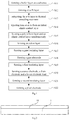
- the method for manufacturing the array substrate includes the following steps.
- Step S11 forming a buffer layer on the substrate.
- the substrate may be subjected to pre-cleaning treatment in accordance with the practical need, and the buffer layer for covering the entire substrate may be formed on the substrate by a coating process.
- the buffer layer 11 is formed on the substrate 1.
- Step S11 is an optional one.
- the buffer layer formed in Step S11 may improve an adhesion degree between the a-Si layer to be formed and the substrate. Meanwhile, it may also prevent metallic ions in the substrate from diffusing toward the ohmic contact layer, and reduce generation of leakage current.
- a material of the substrate is not particularly defined herein.
- the substrate may be a glass substrate or a flexible substrate.
- the buffer layer having a thickness of 2000 to 3000 ⁇ is deposited on the glass substrate by plasma enhanced chemical vapor deposition (PECVD).
- PECVD plasma enhanced chemical vapor deposition
- a reacting gas for forming the SiN x film layer may be a mixture of SiH 4 , NH 3 and N 2 , or a mixture of SiH 2 Cl 2 , NH 3 and N 2 .
- a reacting gas for forming the SiO x film layer may be a mixture of SiH 4 , NH 3 and O 2 , or a mixture of SiH 2 Cl 2 , NH 3 and O 2 .
- Step S12 forming an a-Si layer.
- the a-Si layer for covering the entire substrate (or the buffer layer) may be formed on the substrate (or the buffer layer) by a coating process.
- the a-Si layer 12 for covering the entire buffer layer 11 is formed on the buffer layer 11 shown as Fig.2 by a coating process in Step S12.
- Step S12 the a-Si layer having a thickness of 300 to 1000 ⁇ may be deposited on the substrate (or the buffer layer).
- a reacting gas used for the deposition may be a mixture of SiH 4 and H 2 , or a mixture of SiH 2 Cl 2 and H 2 .
- the a-Si layer obtained in Step S12 is used for forming a poly-silicon layer in Step S15 below.
- Step S13 subjecting the a-Si layer to thermal annealing treatment.
- the a-Si layer is subjected to the thermal annealing treatment, so as to remove H 2 in the a-Si layer, thereby to prevent the occurrence of hydrogen explosion during the laser annealing treatment in a subsequent step.
- a temperature for the thermal annealing treatment may be set in accordance with the practical need.
- a high temperature may be set for the thermal annealing treatment.
- a low temperature may be set for the thermal annealing treatment, as long as the performance of the flexible substrate is not adversely affected.
- Step S13 is also an optional one.
- Step S14 injecting ions into a region where the ohmic contact layer is to be formed by ion injection.
- a pattern of an n-type or p-type doped region is formed on the a-Si layer shown as Fig.3 by a patterning process, and the ions are injected into the n-type or p-type doped region by ion injection, so as to form patterns of a first initial ohmic contact layer 14 and a second initial ohmic contact layer 15, shown as Fig.4 .
- the injected ions may be Boron or Phosphorus ions, and arrows in Fig.4 represent an injection direction of the ions.
- the ions injected into the a-Si layer are inactivated ions, i.e., these ions cannot function as donors or acceptors.
- the ions are injected into a region of the a-Si layer where the first initial ohmic contact layer and the second initial ohmic contact layer are to be formed by using a photoresist layer 29 as a mask plate.
- Step S15 forming the poly-silicon layer and the ohmic contact layer simultaneously through excimer laser annealing treatment.
- the substrate with the a-Si layer, the first initial ohmic contact layer and the second initial ohmic contact layer, or further a lower electrode of an initial storage capacitor, is subjected to the excimer laser annealing treatment, so as to crystallize the a-Si layer into the poly-silicon layer, active the ions in the initial ohmic contact layer and enable the initial ohmic contact layer to form the final ohmic contact layer.
- the first initial ohmic contact layer and the second initial ohmic contact layer are collectively referred to as the initial ohmic contact layer.
- step S15 the poly-silicon layer is formed and the ions are activated through the single excimer laser annealing treatment.
- the ions are activated through the single excimer laser annealing treatment.
- it is able to simplify the process due to the use of a thermal annealing process, and to prevent the formation of a flexible display device from being limited when the substrate is heated due to the ion activation during the thermal annealing treatment.
- due to a high local temperature of the excimer laser annealing treatment it is able to improve the integrity of the lattices in the poly-silicon layer.
- Step S15 it is able to simplify the process for manufacturing the LTPS TFT, improve the performance of the TFT and facilitate the manufacture of the flexible display device.
- an excimer laser (with a wavelength of 308nm) using XeCl, KrF or ArF may be used in the excimer laser annealing treatment. After passing through an optical system, a laser beam becomes a linear light source.
- the excimer laser annealing treatment is performed at a laser pulse frequency of 100 to 400 Hz, a laser overlapping ratio of 90% to 98%, a laser pulse width of less than 100 ns, and a laser energy density of 100 to 600 mJ/cm 2 .
- the a-Si layer is converted into the poly-silicon layer by an excimer laser annealing treatment according to embodiments of the present disclosure, it is able to manufacture the LTPS TFT on the flexible substrate, and to provide the TFT with stable performances.
- a position of the laser beam is constant, and the substrate is fixed onto a translation stage.
- a radiation range of the laser beam is controlled by moving the substrate, so that a predetermined region of the substrate is scanned by the laser beam.
- the a-Si layer and Boron or Phosphorus molecules are melted by absorbing laser energy.
- melted Boron or Phosphorus molecules are doped into the melted silicon in a drive-in diffusion manner.
- the laser-assisted doping is completed when the a-Si layer is crystallized into the poly-silicon layer, so as to form a Boron-doped or Phosphorus-doped poly-silicon region.
- the Boron-doped or Phosphorus-doped poly-silicon region is just a region where the ohmic contact layer is located.
- the a-Si layer and Boron or Phosphorus molecules are melted by absorbing the laser energy under the radiation of laser beam, the melted Boron or Phosphorus molecules are doped into the melted silicon at a rapid rate in a drive-in diffusion manner, and the density of Boron or Phosphorus molecules distributed adjacent to an upper surface of the a-Si layer is similar to that distributed away from the upper surface of the a-Si layer, i.e., there is a relatively small density distribution gradient of the Boron or Phosphorus molecules from the upper surface of the a-Si layer to a lower surface of the a-Si layer. As a result, the resultant ohmic contact layer has excellent conductivity.
- Step S16 forming the active layer.
- the poly-silicon layer obtained in Step S15 is patterned so as to form the active layer at a predetermined region.
- the active layer 17 is formed by a photolithography process.
- a photoresist is used as a mask plate, and the active layer 17 is formed after a dry etching process and the removal of the photoresist.
- the active layer is also referred to as a poly-silicon island.
- Step S17 forming the gate insulating layer.
- the gate insulating (GI) layer 18 having a thickness of 1000 to 2000 ⁇ is deposited by PECVD.
- the GI layer 18 may be a single layer made of SiN x or a double-layered structure consisting of SiN x and SiO x stacked films.
- Step S18 forming the gate electrode.
- a gate metal or alloy layer having a thickness of 1500 to 2500 ⁇ is deposited by sputtering.
- the metal or alloy layer may be made of Mo, Al, Cu or W, or an alloy consisting of at least two of Mo, Al, Cu and W.
- a pattern of the gate electrode 19 is formed on the gate metal or alloy layer by a patterning process.
- Step S19 forming a first insulating layer.
- the first insulating layer 21 is formed on the gate electrode so as to cover the entire substrate.
- an insulating layer having a thickness of 1000 to 3000 ⁇ is deposited by PECVD.
- the insulating layer may be made of SiN x or SiO x .
- the LTPS TFT is formed through the above Steps S11 to S19.
- the method for manufacturing the array substrate further includes a step of forming patterns of the lower electrode 16 and the upper electrode 20 of the storage capacitor.
- Step S14 of injecting the ions into the region where the first initial ohmic contact layer and the second initial ohmic contact layer are to be formed ions are further injected into a region where the lower electrode of the storage capacitor is to be formed, so as to form the lower electrode 16 of the initial storage capacitor.
- the lower electrode of the storage capacitor is formed by doping foreign ions in the a-Si layer, i.e., the foreign ions (B or P ions) are injected into the region of the a-Si layer where the lower electrode of the storage capacitor is to be formed, so as to convert the semiconductive a-Si layer into a conductive layer.
- the foreign ions B or P ions
- Step S18 further includes forming the pattern of the upper electrode 20 of the storage capacitor right above the lower electrode of the storage capacitor. Then, the lower electrode and the upper electrode form the storage capacitor together.
- Step S20 forming a source electrode, a drain electrode and a lower electrode lead. As shown in Fig.7 , the source electrode 22, the drain electrode 23 and the lower electrode lead 24 of the storage capacitor electrically connected to the first initial ohmic contact layer 14 and the second initial ohmic contact layer 15 are formed in Step S20.
- a metal or alloy layer having a thickness of 2000 to 3000 ⁇ is deposited by sputtering or thermal evaporation.
- the metal or alloy layer may be made of Mo, Al, Cu or W, or an alloy thereof.
- Step S21 forming a second insulating layer.
- the second insulating layer 25 is formed on the source electrode 22, the drain electrode 23 and the lower electrode lead 24 in Step S21.
- the second insulating layer having a thickness of 1000 to 3000 ⁇ is deposited by PECVD.
- the second insulating layer may be made of SiN x or SiO x .
- via-holes, in communication with the drain electrode 23 and the lower electrode lead 24, respectively, are formed by a photolithography process and a dry etching process.
- the second insulating layer may also be made of photosensitive, insulating resin.
- Step S22 forming the pixel electrode.
- a transparent conductive film having a thickness of 500 to 1500 ⁇ is deposited by magnetron sputtering.
- the transparent conductive film may be made of ITO, IZO or AlZO.
- an exposure process is performed using a conventional mask plate, and the pixel electrode is then formed after a development process and a wet etching process.
- the present disclosure provides in embodiments the LTPS TFT manufactured by the above-mentioned LTPS TFT manufacturing method.
- the present disclosure further provides in embodiments the array substrate manufactured by the above-mentioned array substrate manufacturing method.
- the ion injection is performed prior to forming the poly-silicon layer, and the ohmic contact layer is formed during the formation of the poly-silicon layer, i.e., the ohmic contact layer formed during the excimer laser annealing treatment.
- the ion injection is performed prior to forming the poly-silicon layer
- the ohmic contact layer is formed during the formation of the poly-silicon layer, i.e., the ohmic contact layer formed during the excimer laser annealing treatment.
Landscapes
- Thin Film Transistor (AREA)
- Engineering & Computer Science (AREA)
- Power Engineering (AREA)
- Physics & Mathematics (AREA)
- Optics & Photonics (AREA)
- Chemical & Material Sciences (AREA)
- Crystallography & Structural Chemistry (AREA)
- Recrystallisation Techniques (AREA)
Description
- The present disclosure relates to the field of thin film transistor (TFT) manufacturing process, in particular to a low temperature poly-silicon (LTPS) TFT, an array substrate, and their manufacturing methods.
- TFTs have been used in pixel units for various display devices so as to drive the display devices by applying a driving voltage, and an a-Si material with excellent stability and processability has always been used for an active layer of the TFT. However, the a-Si material has low carrier mobility, and cannot meet the requirements of a large-size and high-resolution display device, especially a next-generation AMOLED (active matrix organic light-emitting diode) display device. As compared with the a-Si TFT, a poly-silicon TFT, especially an LTPS TFT, has higher carrier mobility, better liquid crystal characteristics and lower leakage current, thus it has gradually replaced the a-Si TFT and become a mainstream of the TFTs.
- In the related art, an active region is formed by ion injection subsequent to the formation of a poly-silicon layer. After the ion injection, doped impurities at the active region are usually positioned on an interstitial lattice site, and thus it is impossible to provide carriers. It is required to activate the ions injected into the poly-silicon layer by a thermal annealing process, so as to recover integrity of the lattices. It can be seen that, in the related art, three steps are desired for the formation of the poly-silicon layer and the active region, so the process thereof is complex. In addition, the thermal annealing process is performed at a high temperature, so it cannot be adapted to the formation of the TFT on a flexible substrate.
-
US 2006/017052 discloses a method for manufaturing a LTPS TFT with an additional annealing step before the excimer laser annealing. - An object of the present disclosure is to provide an LTPS TFT, an array substrate and their manufacturing methods, so as to simplify a process for manufacturing the LTPS TFT.
- In one aspect, the present disclosure provides in embodiments a method for manufacturing an LTPS TFT according to the independent claim.
- Alternatively, the excimer laser annealing treatment is performed at a laser pulse frequency of 100 to 400 Hz, a laser overlapping ratio of 90% to 98%, a laser pulse width of less than 100 ns, and a laser energy density of 100 to 600 mJ/cm2.
- Alternatively, subsequent to forming the a-Si layer and prior to injecting the foreign ions, the method further includes subjecting the a-Si layer to thermal annealing treatment.
- Alternatively, prior to forming the a-Si layer, the method further includes forming a buffer layer on the substrate so as to cover the entire substrate.
- Alternatively, the foreign ion is a boron or phosphorus ion.
- Alternatively, the substrate is a flexible substrate.
- In another aspect, the present provides in embodiments a method for manufacturing an array substrate, including steps of forming an LTPS TFT on a substrate and forming a lower electrode of a storage capacitor. The LTPS TFT is formed by the above-mentioned method.
- Alternatively, the step of forming the lower electrode of the storage capacitor includes: injecting foreign ions into a region of the a-Si layer where the lower electrode of the storage capacitor is to be formed while injecting foreign ions into the region of the a-Si layer where the ohmic contact layer is to be formed by ion injection, so as to enable a lower electrode of an initial storage capacitor to be formed at the region where the lower electrode of the storage capacitor is to be formed.
- According to the method for manufacturing the LTPS TFT in the above-mentioned embodiments, the ion injection is performed prior to the formation of the poly-silicon layer, and the ohmic contact layer is formed during the formation of the poly-silicon layer, i.e., the ohmic contact layer is formed during the excimer laser annealing treatment, as a result, it is able to simplify the manufacturing process. In addition, the foreign ions for the ohmic contact layer are doped through the excimer laser annealing treatment in a drive-in diffusion manner, thereby to prevent the occurrence of defects and imperfections of the TFT due to the ion injection and to improve the performance of the TFT.
-
-
Fig.1 is a flow chart of a method for manufacturing an array substrate according to an embodiment of the present disclosure; -
Fig.2 is a schematic view showing a substrate with a buffer layer according to an embodiment of the present disclosure; -
Fig.3 is a schematic view showing the substrate with an a-Si layer according to an embodiment of the present disclosure; -
Fig.4 is a schematic view showing the substrate with an initial ohmic contact layer according to an embodiment of the present disclosure; -
Fig.5 is a schematic view showing the substrate with an active layer according to an embodiment of the present disclosure; -
Fig.6 is a schematic view showing the substrate with a gate insulating layer, a gate electrode and an upper electrode of a storage capacitor according to an embodiment of the present disclosure; -
Fig.7 is a schematic view showing the substrate with a first insulating layer, an ohmic contact layer, a lower electrode lead according to an embodiment of the present disclosure; and -
Fig.8 is a schematic view showing the substrate with a second insulating layer and a pixel electrode according to an embodiment of the present disclosure. - The present disclosure provides in the following embodiments an LTPS TFT, an array substrate and their manufacturing methods, so as to simplify a process for manufacturing the LTPS TFT and improve the performance of the LTPS TFT.
- According to the method for manufacturing the LTPS TFT in embodiments of the present disclosure, ions are injected into an a-Si layer prior to the formation of a poly-silicon layer, so as to form an initial ohmic contact layer, and an ohmic contact layer with the ions being activated is formed during the formation of the poly-silicon layer, so it is able to simplify the manufacturing process.
- In embodiments of the present disclosure, "ohmic contact layer" is also referred to as a source/drain electrode doped layer, and it includes two regions independent of each other, which are electrically connected to a subsequently-formed source electrode and a subsequently-formed drain electrode, respectively.
- The present disclosure provides in embodiments a method for manufacturing an LTPS TFT, including a step of forming an active layer and an ohmic contact layer on a substrate. The step of forming the active layer and the ohmic contact layer on the substrate includes:
- forming an a-Si layer on the substrate;
- injecting foreign ions into a region of the a-Si layer where the ohmic contact layer is to be formed by ion injection, so as to form an initial ohmic contact layer at the region where the ohmic contact layer is to be formed;
- subjecting the a-Si layer obtained after the ion injection to excimer laser annealing treatment so as to crystallize the a-Si layer into a poly-silicon layer and enable the initial ohmic contact layer to form the final ohmic contact layer; and
- patterning the poly-silicon layer obtained after the excimer laser annealing treatment, so as to form the active layer.
- It should be appreciated by those skilled in the art that, the method for manufacturing the LTPS TFT further includes at least a step of forming a gate insulating layer and a gate electrode on the substrate, which is not particularly defined herein.
- The present disclosure further provides in an embodiment a method for manufacturing an array substrate, including steps of forming an LTPS TFT on a substrate and forming a lower electrode of a storage capacitor, wherein the step of forming the LTPS TFT at least includes forming an active layer and an ohmic contact layer on the substrate, wherein the step of forming the active layer and the ohmic contact layer includes:
- forming an a-Si layer on the substrate;
- injecting foreign ions into a region of the a-Si layer where the ohmic contact layer is to be formed by ion injection, so as to form an initial ohmic contact layer at the region where the ohmic contact layer is to be formed;
- subjecting the a-Si layer obtained after the ion injection to excimer laser annealing treatment so as to crystallize the a-Si layer into a poly-silicon layer and enable the initial ohmic contact layer to form the final ohmic contact layer; and
- patterning the poly-silicon layer obtained after the excimer laser annealing treatment, so as to form the active layer.
- Alternatively, the step of forming the lower electrode of the storage capacitor includes: injecting foreign ions into a region of the a-Si layer where the lower electrode of the storage capacitor is to be formed while injecting foreign ions into the region of the a-Si layer where the ohmic contact layer is to be formed by ion injection, so as to enable a lower electrode of an initial storage capacitor to be formed at the region where the lower electrode of the storage capacitor is to be formed.
- The lower electrode of the storage capacitor is manufactured on the array substrate by a single patterning process at the same time with partial procedures of manufacturing the TFT. The procedures of manufacturing the TFT and the lower electrode of the storage capacitor on the array substrate will be described hereinafter.
- Referring to
Fig.1 , in an alternative embodiment, the method for manufacturing the array substrate includes the following steps. - Step S11: forming a buffer layer on the substrate. When the cleanliness of the substrate does not meet a predetermined requirement, the substrate may be subjected to pre-cleaning treatment in accordance with the practical need, and the buffer layer for covering the entire substrate may be formed on the substrate by a coating process. To be specific, referring to
Fig.2 , thebuffer layer 11 is formed on thesubstrate 1. - Step S11 is an optional one. The buffer layer formed in Step S11 may improve an adhesion degree between the a-Si layer to be formed and the substrate. Meanwhile, it may also prevent metallic ions in the substrate from diffusing toward the ohmic contact layer, and reduce generation of leakage current. A material of the substrate is not particularly defined herein. For example, the substrate may be a glass substrate or a flexible substrate.
- As an alternative mode, in Step S11, the buffer layer having a thickness of 2000 to 3000Å is deposited on the glass substrate by plasma enhanced chemical vapor deposition (PECVD). A single-layered structure consisting of a SiOx or SiNx film layer, or a multi-layered structure consisting of both SiOx and SiNx film layers, may be deposited.
- A reacting gas for forming the SiNx film layer may be a mixture of SiH4, NH3 and N2, or a mixture of SiH2Cl2, NH3 and N2. A reacting gas for forming the SiOx film layer may be a mixture of SiH4, NH3 and O2, or a mixture of SiH2Cl2, NH3 and O2.
- Step S12: forming an a-Si layer. The a-Si layer for covering the entire substrate (or the buffer layer) may be formed on the substrate (or the buffer layer) by a coating process. In this embodiment, because the buffer layer has been formed on the substrate, as shown in
Fig.3 , thea-Si layer 12 for covering theentire buffer layer 11 is formed on thebuffer layer 11 shown asFig.2 by a coating process in Step S12. - As an alternative mode, in Step S12, the a-Si layer having a thickness of 300 to 1000Å may be deposited on the substrate (or the buffer layer). A reacting gas used for the deposition may be a mixture of SiH4 and H2, or a mixture of SiH2Cl2 and H2. The a-Si layer obtained in Step S12 is used for forming a poly-silicon layer in Step S15 below.
- Step S13: subjecting the a-Si layer to thermal annealing treatment. The a-Si layer is subjected to the thermal annealing treatment, so as to remove H2 in the a-Si layer, thereby to prevent the occurrence of hydrogen explosion during the laser annealing treatment in a subsequent step.
- A temperature for the thermal annealing treatment may be set in accordance with the practical need. When a glass substrate is used, a high temperature may be set for the thermal annealing treatment. When a flexible substrate is used, a low temperature may be set for the thermal annealing treatment, as long as the performance of the flexible substrate is not adversely affected. Step S13 is also an optional one.
- Step S14: injecting ions into a region where the ohmic contact layer is to be formed by ion injection. A pattern of an n-type or p-type doped region is formed on the a-Si layer shown as
Fig.3 by a patterning process, and the ions are injected into the n-type or p-type doped region by ion injection, so as to form patterns of a first initialohmic contact layer 14 and a second initialohmic contact layer 15, shown asFig.4 . The injected ions may be Boron or Phosphorus ions, and arrows inFig.4 represent an injection direction of the ions. The ions injected into the a-Si layer are inactivated ions, i.e., these ions cannot function as donors or acceptors. To be specific, referring toFig.4 , the ions are injected into a region of the a-Si layer where the first initial ohmic contact layer and the second initial ohmic contact layer are to be formed by using aphotoresist layer 29 as a mask plate. - Step S15: forming the poly-silicon layer and the ohmic contact layer simultaneously through excimer laser annealing treatment. The substrate with the a-Si layer, the first initial ohmic contact layer and the second initial ohmic contact layer, or further a lower electrode of an initial storage capacitor, is subjected to the excimer laser annealing treatment, so as to crystallize the a-Si layer into the poly-silicon layer, active the ions in the initial ohmic contact layer and enable the initial ohmic contact layer to form the final ohmic contact layer. The first initial ohmic contact layer and the second initial ohmic contact layer are collectively referred to as the initial ohmic contact layer.
- In step S15, the poly-silicon layer is formed and the ions are activated through the single excimer laser annealing treatment. As a result, it is able to simplify the process due to the use of a thermal annealing process, and to prevent the formation of a flexible display device from being limited when the substrate is heated due to the ion activation during the thermal annealing treatment. In addition, due to a high local temperature of the excimer laser annealing treatment, it is able to improve the integrity of the lattices in the poly-silicon layer.
- Through Step S15, it is able to simplify the process for manufacturing the LTPS TFT, improve the performance of the TFT and facilitate the manufacture of the flexible display device. In this embodiment, an excimer laser (with a wavelength of 308nm) using XeCl, KrF or ArF may be used in the excimer laser annealing treatment. After passing through an optical system, a laser beam becomes a linear light source. Alternatively, the excimer laser annealing treatment is performed at a laser pulse frequency of 100 to 400 Hz, a laser overlapping ratio of 90% to 98%, a laser pulse width of less than 100 ns, and a laser energy density of 100 to 600 mJ/cm2.
- As compared with a thermal annealing process, when the a-Si layer is converted into the poly-silicon layer by an excimer laser annealing treatment according to embodiments of the present disclosure, it is able to manufacture the LTPS TFT on the flexible substrate, and to provide the TFT with stable performances.
- During the excimer laser crystallization (ELA), a position of the laser beam is constant, and the substrate is fixed onto a translation stage. A radiation range of the laser beam is controlled by moving the substrate, so that a predetermined region of the substrate is scanned by the laser beam. Under the radiation of the laser beam, the a-Si layer and Boron or Phosphorus molecules are melted by absorbing laser energy. At this time, melted Boron or Phosphorus molecules are doped into the melted silicon in a drive-in diffusion manner. During a cooling procedure, the laser-assisted doping is completed when the a-Si layer is crystallized into the poly-silicon layer, so as to form a Boron-doped or Phosphorus-doped poly-silicon region. The Boron-doped or Phosphorus-doped poly-silicon region is just a region where the ohmic contact layer is located. In this procedure, when the a-Si layer and Boron or Phosphorus molecules are melted by absorbing the laser energy under the radiation of laser beam, the melted Boron or Phosphorus molecules are doped into the melted silicon at a rapid rate in a drive-in diffusion manner, and the density of Boron or Phosphorus molecules distributed adjacent to an upper surface of the a-Si layer is similar to that distributed away from the upper surface of the a-Si layer, i.e., there is a relatively small density distribution gradient of the Boron or Phosphorus molecules from the upper surface of the a-Si layer to a lower surface of the a-Si layer. As a result, the resultant ohmic contact layer has excellent conductivity.
- Step S16: forming the active layer. The poly-silicon layer obtained in Step S15 is patterned so as to form the active layer at a predetermined region. During the implementation, referring to
Fig.5 , theactive layer 17 is formed by a photolithography process. To be specific, a photoresist is used as a mask plate, and theactive layer 17 is formed after a dry etching process and the removal of the photoresist. In embodiments of the present disclosure, the active layer is also referred to as a poly-silicon island. - Step S17: forming the gate insulating layer. Referring to
Fig.6 , the gate insulating (GI)layer 18 having a thickness of 1000 to 2000Å is deposited by PECVD. TheGI layer 18 may be a single layer made of SiNx or a double-layered structure consisting of SiNx and SiOx stacked films. - Step S18: forming the gate electrode. Referring to
Fig.6 , a gate metal or alloy layer having a thickness of 1500 to 2500Å is deposited by sputtering. The metal or alloy layer may be made of Mo, Al, Cu or W, or an alloy consisting of at least two of Mo, Al, Cu and W. Then, a pattern of thegate electrode 19 is formed on the gate metal or alloy layer by a patterning process. - Step S19: forming a first insulating layer. As shown in
Fig.7 , the first insulatinglayer 21 is formed on the gate electrode so as to cover the entire substrate. To be specific, an insulating layer having a thickness of 1000 to 3000Å is deposited by PECVD. The insulating layer may be made of SiNx or SiOx. Then, via-holes, in communication with the first initialohmic contact layer 14 and the second initialohmic contact layer 15, respectively, are formed after a photolithography process and a dry etching process. - The LTPS TFT is formed through the above Steps S11 to S19.
- Further, subsequent to the formation of the LTPS TFT through Steps S11 to S19, the method for manufacturing the array substrate further includes a step of forming patterns of the
lower electrode 16 and theupper electrode 20 of the storage capacitor. - Alternatively, for the poly-silicon layer, subsequent to Step S14 of injecting the ions into the region where the first initial ohmic contact layer and the second initial ohmic contact layer are to be formed, ions are further injected into a region where the lower electrode of the storage capacitor is to be formed, so as to form the
lower electrode 16 of the initial storage capacitor. - The lower electrode of the storage capacitor is formed by doping foreign ions in the a-Si layer, i.e., the foreign ions (B or P ions) are injected into the region of the a-Si layer where the lower electrode of the storage capacitor is to be formed, so as to convert the semiconductive a-Si layer into a conductive layer.
- Alternatively, during the formation of the pattern of the
gate electrode 19 by a patterning process, Step S18 further includes forming the pattern of theupper electrode 20 of the storage capacitor right above the lower electrode of the storage capacitor. Then, the lower electrode and the upper electrode form the storage capacitor together. - Step S20: forming a source electrode, a drain electrode and a lower electrode lead. As shown in
Fig.7 , thesource electrode 22, thedrain electrode 23 and thelower electrode lead 24 of the storage capacitor electrically connected to the first initialohmic contact layer 14 and the second initialohmic contact layer 15 are formed in Step S20. - To be specific, a metal or alloy layer having a thickness of 2000 to 3000Å is deposited by sputtering or thermal evaporation. The metal or alloy layer may be made of Mo, Al, Cu or W, or an alloy thereof. Then, the
source electrode 22, thedrain electrode 23 and thelower electrode lead 24 of the storage capacitor are formed after a photolithography process and an etching process, as shown inFig.7 . - Step S21: forming a second insulating layer. As shown in
Fig.8 , the second insulatinglayer 25 is formed on thesource electrode 22, thedrain electrode 23 and thelower electrode lead 24 in Step S21. To be specific, the second insulating layer having a thickness of 1000 to 3000Å is deposited by PECVD. The second insulating layer may be made of SiNx or SiOx. Then, via-holes, in communication with thedrain electrode 23 and thelower electrode lead 24, respectively, are formed by a photolithography process and a dry etching process. In addition, the second insulating layer may also be made of photosensitive, insulating resin. - Step S22: forming the pixel electrode. As shown in
Fig.8 , thepixel electrode 26, connected to the drain electrode and the lower electrode of the storage capacitor through the via-holes, respectively, is formed on the second insulatinglayer 25 in Step S22. To be specific, a transparent conductive film having a thickness of 500 to 1500Å is deposited by magnetron sputtering. The transparent conductive film may be made of ITO, IZO or AlZO. Then, an exposure process is performed using a conventional mask plate, and the pixel electrode is then formed after a development process and a wet etching process. - The present disclosure provides in embodiments the LTPS TFT manufactured by the above-mentioned LTPS TFT manufacturing method.
- The present disclosure further provides in embodiments the array substrate manufactured by the above-mentioned array substrate manufacturing method.
- According to the method for manufacturing the LTPS TFT in the above-mentioned embodiments, the ion injection is performed prior to forming the poly-silicon layer, and the ohmic contact layer is formed during the formation of the poly-silicon layer, i.e., the ohmic contact layer formed during the excimer laser annealing treatment. As a result, it is able to simplify the manufacturing process and inject the impurity ions for the ohmic contact layer through the excimer laser annealing treatment, thereby to prevent the occurrence of defects and imperfections of the TFT due to the ion injection and to improve the performance of the TFT.
Claims (8)
- A method for manufacturing a low temperature poly-silicon (LTPS) thin film transistor (TFT), comprising a step of forming an active layer and an ohmic contact layer on a substrate, wherein the step of forming the active layer and the ohmic contact layer on the substrate comprises:forming an a-Si layer on the substrate;injecting foreign ions into a region of the a-Si layer where the ohmic contact layer is to be formed by ion injection, so as to form an initial ohmic contact layer at the region where the ohmic contact layer is to be formed, and refraining injecting the foreign ions into other region of the a-Si layer corresponding to a region occupied by the LTPS TFT in addition to the region of the a-Si layer where the ohmic contact layer is to be formed;subjecting the a-Si layer obtained after the ion injection without an annealing step in between to excimer laser annealing treatment so as to crystallize the a-Si layer into a poly-silicon layer, activate the injected ions and enable the initial ohmic contact layer to form the final ohmic contact layer; andpatterning the poly-silicon layer obtained after the excimer laser annealing treatment, so as to form the active layer, wherein in the region occupied by the LTPS TFT, the poly-silicon layer located at a side of the ohmic contact layer away from the active layer is completely removed.
- The method according to claim 1, wherein the excimer laser annealing treatment is performed at a laser pulse frequency of 100 to 400 Hz, a laser overlapping ratio of 90% to 98%, a laser pulse width of less than 100 ns, and a laser energy density of 100 to 600 mJ/cm2.
- The method according to claim 1 or 2, wherein subsequent to forming the a-Si layer and prior to injecting the foreign ions, the method further comprises subjecting the a-Si layer to thermal annealing treatment.
- The method according to any one of claims 1 to 3, wherein prior to forming the a-Si layer, the method further comprises forming a buffer layer on the substrate so as to cover the entire substrate.
- The method according to any one of claims 1 to 4, wherein the foreign ion is a boron or phosphorus ion.
- The method according to any one of claims 1 to 5, wherein the substrate is a flexible substrate.
- A method for manufacturing an array substrate, comprising steps of forming an LTPS TFT on a substrate and forming a lower electrode of a storage capacitor, wherein the LTPS TFT is formed by the method according to any one of claims 1 to 6.
- The method according to claim 7, wherein the step of forming the lower electrode of the storage capacitor comprises injecting foreign ions into a region of the a-Si layer where the lower electrode of the storage capacitor is to be formed while injecting foreign ions into the region of the a-Si layer where the ohmic contact layer is to be formed by ion injection, so as to enable a lower electrode of an initial storage capacitor to be formed at the region where the lower electrode of the storage capacitor is to be formed.
Applications Claiming Priority (2)
| Application Number | Priority Date | Filing Date | Title |
|---|---|---|---|
| CN201410062345.XA CN103839825A (en) | 2014-02-24 | 2014-02-24 | Low-temperature polycrystalline silicon thin film transistor, array substrate and manufacturing method of array substrate |
| PCT/CN2014/073615 WO2015123903A1 (en) | 2014-02-24 | 2014-03-18 | Low-temperature polycrystalline silicon thin-film transistor, array substrate and manufacturing method therefor |
Publications (3)
| Publication Number | Publication Date |
|---|---|
| EP3113217A1 EP3113217A1 (en) | 2017-01-04 |
| EP3113217A4 EP3113217A4 (en) | 2017-03-01 |
| EP3113217B1 true EP3113217B1 (en) | 2020-03-11 |
Family
ID=50803208
Family Applications (1)
| Application Number | Title | Priority Date | Filing Date |
|---|---|---|---|
| EP14859331.2A Active EP3113217B1 (en) | 2014-02-24 | 2014-03-18 | Low-temperature polycrystalline silicon thin-film transistor, array substrate and manufacturing method therefor |
Country Status (4)
| Country | Link |
|---|---|
| US (1) | US20160043114A1 (en) |
| EP (1) | EP3113217B1 (en) |
| CN (1) | CN103839825A (en) |
| WO (1) | WO2015123903A1 (en) |
Families Citing this family (18)
| Publication number | Priority date | Publication date | Assignee | Title |
|---|---|---|---|---|
| CN103390592B (en) * | 2013-07-17 | 2016-02-24 | 京东方科技集团股份有限公司 | Array base palte preparation method, array base palte and display unit |
| CN104900491A (en) * | 2015-05-05 | 2015-09-09 | 京东方科技集团股份有限公司 | Thin film transistor and manufacturing method thereof and display device |
| CN104979215B (en) | 2015-06-23 | 2018-01-02 | 京东方科技集团股份有限公司 | Low-temperature polysilicon film transistor and preparation method thereof |
| CN105140238A (en) * | 2015-08-05 | 2015-12-09 | 深圳市华星光电技术有限公司 | Array substrate and fabrication method thereof |
| CN105206569A (en) * | 2015-10-23 | 2015-12-30 | 京东方科技集团股份有限公司 | Array substrate, manufacturing method thereof, display panel and display device |
| CN105633076A (en) * | 2016-01-04 | 2016-06-01 | 京东方科技集团股份有限公司 | Display substrate, manufacturing method thereof and display device |
| CN105759527A (en) * | 2016-04-26 | 2016-07-13 | 上海天马有机发光显示技术有限公司 | Array substrate, manufacturing method of array substrate and display panel |
| CN107636839B (en) * | 2016-07-25 | 2020-12-04 | 京东方科技集团股份有限公司 | Polysilicon thin film transistor, method for manufacturing the same, and display device |
| WO2018119649A1 (en) * | 2016-12-27 | 2018-07-05 | 深圳市柔宇科技有限公司 | Array substrate and method for preparing array substrate |
| CN107093633B (en) * | 2017-04-21 | 2020-04-03 | 京东方科技集团股份有限公司 | Thin film transistor and its manufacturing method, array substrate, display device |
| CN107393830A (en) * | 2017-07-21 | 2017-11-24 | 京东方科技集团股份有限公司 | The preparation method of thin film transistor (TFT) |
| CN108320668A (en) * | 2018-01-19 | 2018-07-24 | 昆山国显光电有限公司 | Flexible display substrates and preparation method thereof |
| CN109637932B (en) * | 2018-11-30 | 2020-11-10 | 武汉华星光电技术有限公司 | Thin film transistor and preparation method thereof |
| US11888034B2 (en) | 2019-06-07 | 2024-01-30 | Intel Corporation | Transistors with metal chalcogenide channel materials |
| US11777029B2 (en) | 2019-06-27 | 2023-10-03 | Intel Corporation | Vertical transistors for ultra-dense logic and memory applications |
| US11171243B2 (en) | 2019-06-27 | 2021-11-09 | Intel Corporation | Transistor structures with a metal oxide contact buffer |
| CN112707366A (en) * | 2020-12-29 | 2021-04-27 | 无锡中微晶园电子有限公司 | High-precision polycrystalline low-resistance process manufacturing technology |
| CN113745099A (en) * | 2021-09-06 | 2021-12-03 | 长江存储科技有限责任公司 | Polycrystalline silicon layer, manufacturing method thereof and semiconductor device |
Family Cites Families (23)
| Publication number | Priority date | Publication date | Assignee | Title |
|---|---|---|---|---|
| JP3211340B2 (en) * | 1992-02-19 | 2001-09-25 | カシオ計算機株式会社 | Method for manufacturing thin film transistor |
| KR100355938B1 (en) * | 1993-05-26 | 2002-12-16 | 가부시키가이샤 한도오따이 에네루기 켄큐쇼 | Semiconductor device manufacturing method |
| JPH08242001A (en) * | 1995-03-06 | 1996-09-17 | Toshiba Corp | Method for manufacturing thin film transistor |
| JPH09107102A (en) * | 1995-10-09 | 1997-04-22 | Sharp Corp | Thin film transistor and method of manufacturing the same |
| JPH1079514A (en) * | 1996-09-05 | 1998-03-24 | Toshiba Corp | Active matrix substrate manufacturing method |
| JP3483484B2 (en) * | 1998-12-28 | 2004-01-06 | 富士通ディスプレイテクノロジーズ株式会社 | Semiconductor device, image display device, method of manufacturing semiconductor device, and method of manufacturing image display device |
| KR100333276B1 (en) * | 1999-05-20 | 2002-04-24 | 구본준, 론 위라하디락사 | TFT of LCD device and the same methode |
| KR100424593B1 (en) * | 2001-06-07 | 2004-03-27 | 엘지.필립스 엘시디 주식회사 | A method of crystallizing Si |
| US6773467B2 (en) * | 2002-06-03 | 2004-08-10 | Toppoly Optoelectronics Corp. | Storage capacitor of planar display and process for fabricating same |
| KR100640213B1 (en) * | 2003-12-29 | 2006-10-31 | 엘지.필립스 엘시디 주식회사 | Polysilicon Liquid Crystal Display Device Manufacturing Method |
| KR100616708B1 (en) * | 2004-04-12 | 2006-08-28 | 엘지.필립스 엘시디 주식회사 | LCD array substrate and manufacturing method thereof |
| KR100685396B1 (en) * | 2004-07-22 | 2007-02-22 | 삼성에스디아이 주식회사 | Method for manufacturing semiconductor device and semiconductor device manufactured by this method |
| US7410882B2 (en) * | 2004-09-28 | 2008-08-12 | Palo Alto Research Center Incorporated | Method of manufacturing and structure of polycrystalline semiconductor thin-film heterostructures on dissimilar substrates |
| KR100710960B1 (en) * | 2004-09-29 | 2007-04-24 | 호야 가부시키가이샤 | Mask blank substrate, mask blank, exposure mask, mask blank substrate manufacturing method, and semiconductor manufacturing method |
| JP2006133285A (en) * | 2004-11-02 | 2006-05-25 | Mitsubishi Electric Corp | Display device and manufacturing method thereof |
| KR100689818B1 (en) * | 2004-11-05 | 2007-03-08 | 삼성전자주식회사 | Method for forming single crystal semiconductor thin film on insulating layer and semiconductor device manufactured thereby |
| JP4957942B2 (en) * | 2005-08-05 | 2012-06-20 | Nltテクノロジー株式会社 | Manufacturing method of semiconductor device provided with thin film transistor |
| TWI328259B (en) * | 2007-05-15 | 2010-08-01 | Au Optronics Corp | Semiconductor device and manufacturing method thereof |
| JP5697634B2 (en) * | 2011-07-26 | 2015-04-08 | 富士フイルム株式会社 | Optical film, security product, and authentication method |
| CN102945789B (en) * | 2012-11-22 | 2015-07-22 | 京东方科技集团股份有限公司 | Preparation method of low-temperature polycrystalline silicon film, thin-film transistor and preparation method of thin-film transistor |
| CN103107095A (en) * | 2013-01-25 | 2013-05-15 | 京东方科技集团股份有限公司 | Thin film transistor, manufacturing method of thin film transistor, array substrate and display device |
| CN103390592B (en) * | 2013-07-17 | 2016-02-24 | 京东方科技集团股份有限公司 | Array base palte preparation method, array base palte and display unit |
| KR102074431B1 (en) * | 2013-07-19 | 2020-03-03 | 삼성디스플레이 주식회사 | Thin film transistor substrate and the method therefor, organic light emitting display comprising the same |
-
2014
- 2014-02-24 CN CN201410062345.XA patent/CN103839825A/en active Pending
- 2014-03-18 US US14/434,856 patent/US20160043114A1/en not_active Abandoned
- 2014-03-18 EP EP14859331.2A patent/EP3113217B1/en active Active
- 2014-03-18 WO PCT/CN2014/073615 patent/WO2015123903A1/en not_active Ceased
Non-Patent Citations (1)
| Title |
|---|
| None * |
Also Published As
| Publication number | Publication date |
|---|---|
| US20160043114A1 (en) | 2016-02-11 |
| CN103839825A (en) | 2014-06-04 |
| WO2015123903A1 (en) | 2015-08-27 |
| EP3113217A4 (en) | 2017-03-01 |
| EP3113217A1 (en) | 2017-01-04 |
Similar Documents
| Publication | Publication Date | Title |
|---|---|---|
| EP3113217A1 (en) | Low-temperature polycrystalline silicon thin-film transistor, array substrate and manufacturing method therefor | |
| US7915689B2 (en) | Thin film transistor, display device including the same and manufacturing method thereof | |
| CN103839826B (en) | Low-temperature polycrystalline silicon thin film transistor, array substrate and manufacturing method of array substrate | |
| US10224416B2 (en) | Method for manufacturing low-temperature poly-silicon thin film transistor, low-temperature poly-silicon thin film transistor and display device | |
| US10978495B2 (en) | Array substrate and method of manufacturing the same, and display device | |
| US10700107B2 (en) | Low-temperature polysilicon thin film transistor, method of manufacturing the same, and display substrate | |
| US9520421B1 (en) | Method for manufacturing LTPS TFT substrate and LTPS TFT substrate | |
| CN100361271C (en) | Mask for polycrystallization and method of manufacturing thin film transistor using same | |
| TWI578443B (en) | Polycrystalline germanium thin film transistor element and manufacturing method thereof | |
| JP2008252108A (en) | Semiconductor device | |
| US20060060848A1 (en) | Semiconductor device and method of fabricating a ltps film | |
| WO2016201725A1 (en) | Method for manufacturing low-temperature polysilicon thin film transistor (tft) substrate and low-temperature polysilicon tft substrate | |
| WO2020062426A1 (en) | Array substrate and preparation method therefor, and display device | |
| JPH0437144A (en) | Manufacture of thin film transistor | |
| WO2017028499A1 (en) | Low-temperature polycrystalline silicon thin film, thin film transistor and respective preparation method and display device | |
| KR20000017056A (en) | Semiconductor device manufacturing method | |
| WO2016165223A1 (en) | Polycrystalline silicon thin-film transistor, manufacturing method therefor, and display device | |
| CN108831894A (en) | Production method, low-temperature polysilicon film and the low temperature polycrystalline silicon TFT substrate of low-temperature polysilicon film | |
| US20190221672A1 (en) | Low temperature polysilicon thin film transistor and preparation method thereof | |
| US7026201B2 (en) | Method for forming polycrystalline silicon thin film transistor | |
| KR100867921B1 (en) | Manufacturing Method of Thin Film Transistor | |
| JP4155039B2 (en) | Thin film transistor, electro-optical device, electronic equipment | |
| KR100796613B1 (en) | Polycrystalline Silicon Crystallization Method Using Laser and Manufacturing Method of Thin Film Transistor Using The Same | |
| KR100683664B1 (en) | Thin film transistor, method of manufacturing thin film transistor and flat panel display device having same | |
| KR101686242B1 (en) | Method for manufacturing of Thin Film Transistor |
Legal Events
| Date | Code | Title | Description |
|---|---|---|---|
| PUAI | Public reference made under article 153(3) epc to a published international application that has entered the european phase |
Free format text: ORIGINAL CODE: 0009012 |
|
| STAA | Information on the status of an ep patent application or granted ep patent |
Free format text: STATUS: REQUEST FOR EXAMINATION WAS MADE |
|
| 17P | Request for examination filed |
Effective date: 20160513 |
|
| AK | Designated contracting states |
Kind code of ref document: A1 Designated state(s): AL AT BE BG CH CY CZ DE DK EE ES FI FR GB GR HR HU IE IS IT LI LT LU LV MC MK MT NL NO PL PT RO RS SE SI SK SM TR |
|
| AX | Request for extension of the european patent |
Extension state: BA ME |
|
| REG | Reference to a national code |
Ref country code: DE Ref legal event code: R079 Ref document number: 602014062325 Country of ref document: DE Free format text: PREVIOUS MAIN CLASS: H01L0021840000 Ipc: H01L0021336000 |
|
| A4 | Supplementary search report drawn up and despatched |
Effective date: 20170127 |
|
| RIC1 | Information provided on ipc code assigned before grant |
Ipc: H01L 27/12 20060101ALI20170123BHEP Ipc: H01L 29/786 20060101ALI20170123BHEP Ipc: H01L 21/336 20060101AFI20170123BHEP |
|
| DAX | Request for extension of the european patent (deleted) | ||
| GRAP | Despatch of communication of intention to grant a patent |
Free format text: ORIGINAL CODE: EPIDOSNIGR1 |
|
| STAA | Information on the status of an ep patent application or granted ep patent |
Free format text: STATUS: GRANT OF PATENT IS INTENDED |
|
| INTG | Intention to grant announced |
Effective date: 20191029 |
|
| GRAS | Grant fee paid |
Free format text: ORIGINAL CODE: EPIDOSNIGR3 |
|
| GRAA | (expected) grant |
Free format text: ORIGINAL CODE: 0009210 |
|
| STAA | Information on the status of an ep patent application or granted ep patent |
Free format text: STATUS: THE PATENT HAS BEEN GRANTED |
|
| AK | Designated contracting states |
Kind code of ref document: B1 Designated state(s): AL AT BE BG CH CY CZ DE DK EE ES FI FR GB GR HR HU IE IS IT LI LT LU LV MC MK MT NL NO PL PT RO RS SE SI SK SM TR |
|
| REG | Reference to a national code |
Ref country code: GB Ref legal event code: FG4D |
|
| REG | Reference to a national code |
Ref country code: CH Ref legal event code: EP |
|
| REG | Reference to a national code |
Ref country code: AT Ref legal event code: REF Ref document number: 1244193 Country of ref document: AT Kind code of ref document: T Effective date: 20200315 |
|
| REG | Reference to a national code |
Ref country code: IE Ref legal event code: FG4D |
|
| REG | Reference to a national code |
Ref country code: DE Ref legal event code: R096 Ref document number: 602014062325 Country of ref document: DE |
|
| PG25 | Lapsed in a contracting state [announced via postgrant information from national office to epo] |
Ref country code: FI Free format text: LAPSE BECAUSE OF FAILURE TO SUBMIT A TRANSLATION OF THE DESCRIPTION OR TO PAY THE FEE WITHIN THE PRESCRIBED TIME-LIMIT Effective date: 20200311 Ref country code: RS Free format text: LAPSE BECAUSE OF FAILURE TO SUBMIT A TRANSLATION OF THE DESCRIPTION OR TO PAY THE FEE WITHIN THE PRESCRIBED TIME-LIMIT Effective date: 20200311 Ref country code: NO Free format text: LAPSE BECAUSE OF FAILURE TO SUBMIT A TRANSLATION OF THE DESCRIPTION OR TO PAY THE FEE WITHIN THE PRESCRIBED TIME-LIMIT Effective date: 20200611 |
|
| REG | Reference to a national code |
Ref country code: NL Ref legal event code: MP Effective date: 20200311 |
|
| PG25 | Lapsed in a contracting state [announced via postgrant information from national office to epo] |
Ref country code: HR Free format text: LAPSE BECAUSE OF FAILURE TO SUBMIT A TRANSLATION OF THE DESCRIPTION OR TO PAY THE FEE WITHIN THE PRESCRIBED TIME-LIMIT Effective date: 20200311 Ref country code: SE Free format text: LAPSE BECAUSE OF FAILURE TO SUBMIT A TRANSLATION OF THE DESCRIPTION OR TO PAY THE FEE WITHIN THE PRESCRIBED TIME-LIMIT Effective date: 20200311 Ref country code: LV Free format text: LAPSE BECAUSE OF FAILURE TO SUBMIT A TRANSLATION OF THE DESCRIPTION OR TO PAY THE FEE WITHIN THE PRESCRIBED TIME-LIMIT Effective date: 20200311 Ref country code: GR Free format text: LAPSE BECAUSE OF FAILURE TO SUBMIT A TRANSLATION OF THE DESCRIPTION OR TO PAY THE FEE WITHIN THE PRESCRIBED TIME-LIMIT Effective date: 20200612 Ref country code: BG Free format text: LAPSE BECAUSE OF FAILURE TO SUBMIT A TRANSLATION OF THE DESCRIPTION OR TO PAY THE FEE WITHIN THE PRESCRIBED TIME-LIMIT Effective date: 20200611 |
|
| REG | Reference to a national code |
Ref country code: LT Ref legal event code: MG4D |
|
| PG25 | Lapsed in a contracting state [announced via postgrant information from national office to epo] |
Ref country code: NL Free format text: LAPSE BECAUSE OF FAILURE TO SUBMIT A TRANSLATION OF THE DESCRIPTION OR TO PAY THE FEE WITHIN THE PRESCRIBED TIME-LIMIT Effective date: 20200311 |
|
| PG25 | Lapsed in a contracting state [announced via postgrant information from national office to epo] |
Ref country code: CZ Free format text: LAPSE BECAUSE OF FAILURE TO SUBMIT A TRANSLATION OF THE DESCRIPTION OR TO PAY THE FEE WITHIN THE PRESCRIBED TIME-LIMIT Effective date: 20200311 Ref country code: RO Free format text: LAPSE BECAUSE OF FAILURE TO SUBMIT A TRANSLATION OF THE DESCRIPTION OR TO PAY THE FEE WITHIN THE PRESCRIBED TIME-LIMIT Effective date: 20200311 Ref country code: IS Free format text: LAPSE BECAUSE OF FAILURE TO SUBMIT A TRANSLATION OF THE DESCRIPTION OR TO PAY THE FEE WITHIN THE PRESCRIBED TIME-LIMIT Effective date: 20200711 Ref country code: SK Free format text: LAPSE BECAUSE OF FAILURE TO SUBMIT A TRANSLATION OF THE DESCRIPTION OR TO PAY THE FEE WITHIN THE PRESCRIBED TIME-LIMIT Effective date: 20200311 Ref country code: PT Free format text: LAPSE BECAUSE OF FAILURE TO SUBMIT A TRANSLATION OF THE DESCRIPTION OR TO PAY THE FEE WITHIN THE PRESCRIBED TIME-LIMIT Effective date: 20200805 Ref country code: LT Free format text: LAPSE BECAUSE OF FAILURE TO SUBMIT A TRANSLATION OF THE DESCRIPTION OR TO PAY THE FEE WITHIN THE PRESCRIBED TIME-LIMIT Effective date: 20200311 Ref country code: EE Free format text: LAPSE BECAUSE OF FAILURE TO SUBMIT A TRANSLATION OF THE DESCRIPTION OR TO PAY THE FEE WITHIN THE PRESCRIBED TIME-LIMIT Effective date: 20200311 Ref country code: SM Free format text: LAPSE BECAUSE OF FAILURE TO SUBMIT A TRANSLATION OF THE DESCRIPTION OR TO PAY THE FEE WITHIN THE PRESCRIBED TIME-LIMIT Effective date: 20200311 |
|
| REG | Reference to a national code |
Ref country code: CH Ref legal event code: PL |
|
| REG | Reference to a national code |
Ref country code: AT Ref legal event code: MK05 Ref document number: 1244193 Country of ref document: AT Kind code of ref document: T Effective date: 20200311 |
|
| REG | Reference to a national code |
Ref country code: DE Ref legal event code: R097 Ref document number: 602014062325 Country of ref document: DE |
|
| REG | Reference to a national code |
Ref country code: BE Ref legal event code: MM Effective date: 20200331 |
|
| PG25 | Lapsed in a contracting state [announced via postgrant information from national office to epo] |
Ref country code: MC Free format text: LAPSE BECAUSE OF FAILURE TO SUBMIT A TRANSLATION OF THE DESCRIPTION OR TO PAY THE FEE WITHIN THE PRESCRIBED TIME-LIMIT Effective date: 20200311 Ref country code: LU Free format text: LAPSE BECAUSE OF NON-PAYMENT OF DUE FEES Effective date: 20200318 |
|
| PLBE | No opposition filed within time limit |
Free format text: ORIGINAL CODE: 0009261 |
|
| STAA | Information on the status of an ep patent application or granted ep patent |
Free format text: STATUS: NO OPPOSITION FILED WITHIN TIME LIMIT |
|
| PG25 | Lapsed in a contracting state [announced via postgrant information from national office to epo] |
Ref country code: LI Free format text: LAPSE BECAUSE OF NON-PAYMENT OF DUE FEES Effective date: 20200331 Ref country code: DK Free format text: LAPSE BECAUSE OF FAILURE TO SUBMIT A TRANSLATION OF THE DESCRIPTION OR TO PAY THE FEE WITHIN THE PRESCRIBED TIME-LIMIT Effective date: 20200311 Ref country code: AT Free format text: LAPSE BECAUSE OF FAILURE TO SUBMIT A TRANSLATION OF THE DESCRIPTION OR TO PAY THE FEE WITHIN THE PRESCRIBED TIME-LIMIT Effective date: 20200311 Ref country code: CH Free format text: LAPSE BECAUSE OF NON-PAYMENT OF DUE FEES Effective date: 20200331 Ref country code: IE Free format text: LAPSE BECAUSE OF NON-PAYMENT OF DUE FEES Effective date: 20200318 Ref country code: ES Free format text: LAPSE BECAUSE OF FAILURE TO SUBMIT A TRANSLATION OF THE DESCRIPTION OR TO PAY THE FEE WITHIN THE PRESCRIBED TIME-LIMIT Effective date: 20200311 Ref country code: IT Free format text: LAPSE BECAUSE OF FAILURE TO SUBMIT A TRANSLATION OF THE DESCRIPTION OR TO PAY THE FEE WITHIN THE PRESCRIBED TIME-LIMIT Effective date: 20200311 |
|
| 26N | No opposition filed |
Effective date: 20201214 |
|
| PG25 | Lapsed in a contracting state [announced via postgrant information from national office to epo] |
Ref country code: BE Free format text: LAPSE BECAUSE OF NON-PAYMENT OF DUE FEES Effective date: 20200331 Ref country code: SI Free format text: LAPSE BECAUSE OF FAILURE TO SUBMIT A TRANSLATION OF THE DESCRIPTION OR TO PAY THE FEE WITHIN THE PRESCRIBED TIME-LIMIT Effective date: 20200311 Ref country code: PL Free format text: LAPSE BECAUSE OF FAILURE TO SUBMIT A TRANSLATION OF THE DESCRIPTION OR TO PAY THE FEE WITHIN THE PRESCRIBED TIME-LIMIT Effective date: 20200311 |
|
| GBPC | Gb: european patent ceased through non-payment of renewal fee |
Effective date: 20200611 |
|
| PG25 | Lapsed in a contracting state [announced via postgrant information from national office to epo] |
Ref country code: FR Free format text: LAPSE BECAUSE OF NON-PAYMENT OF DUE FEES Effective date: 20200511 Ref country code: GB Free format text: LAPSE BECAUSE OF NON-PAYMENT OF DUE FEES Effective date: 20200611 |
|
| PG25 | Lapsed in a contracting state [announced via postgrant information from national office to epo] |
Ref country code: TR Free format text: LAPSE BECAUSE OF FAILURE TO SUBMIT A TRANSLATION OF THE DESCRIPTION OR TO PAY THE FEE WITHIN THE PRESCRIBED TIME-LIMIT Effective date: 20200311 Ref country code: MT Free format text: LAPSE BECAUSE OF FAILURE TO SUBMIT A TRANSLATION OF THE DESCRIPTION OR TO PAY THE FEE WITHIN THE PRESCRIBED TIME-LIMIT Effective date: 20200311 Ref country code: CY Free format text: LAPSE BECAUSE OF FAILURE TO SUBMIT A TRANSLATION OF THE DESCRIPTION OR TO PAY THE FEE WITHIN THE PRESCRIBED TIME-LIMIT Effective date: 20200311 |
|
| PG25 | Lapsed in a contracting state [announced via postgrant information from national office to epo] |
Ref country code: MK Free format text: LAPSE BECAUSE OF FAILURE TO SUBMIT A TRANSLATION OF THE DESCRIPTION OR TO PAY THE FEE WITHIN THE PRESCRIBED TIME-LIMIT Effective date: 20200311 Ref country code: AL Free format text: LAPSE BECAUSE OF FAILURE TO SUBMIT A TRANSLATION OF THE DESCRIPTION OR TO PAY THE FEE WITHIN THE PRESCRIBED TIME-LIMIT Effective date: 20200311 |
|
| PGFP | Annual fee paid to national office [announced via postgrant information from national office to epo] |
Ref country code: DE Payment date: 20230216 Year of fee payment: 10 |
|
| REG | Reference to a national code |
Ref country code: DE Ref legal event code: R119 Ref document number: 602014062325 Country of ref document: DE |
|
| PG25 | Lapsed in a contracting state [announced via postgrant information from national office to epo] |
Ref country code: DE Free format text: LAPSE BECAUSE OF NON-PAYMENT OF DUE FEES Effective date: 20241001 |
|
| PG25 | Lapsed in a contracting state [announced via postgrant information from national office to epo] |
Ref country code: DE Free format text: LAPSE BECAUSE OF NON-PAYMENT OF DUE FEES Effective date: 20241001 |