EP3107149B1 - Flexible gedruckte leiterplatte umfassend einer kontaktlosen kommunikationsantenne und baugruppe für zahlungsterminal umfassend solch einer flexiblen gedruckten leiterplatte - Google Patents
Flexible gedruckte leiterplatte umfassend einer kontaktlosen kommunikationsantenne und baugruppe für zahlungsterminal umfassend solch einer flexiblen gedruckten leiterplatte Download PDFInfo
- Publication number
- EP3107149B1 EP3107149B1 EP16174869.4A EP16174869A EP3107149B1 EP 3107149 B1 EP3107149 B1 EP 3107149B1 EP 16174869 A EP16174869 A EP 16174869A EP 3107149 B1 EP3107149 B1 EP 3107149B1
- Authority
- EP
- European Patent Office
- Prior art keywords
- printed circuit
- flexible printed
- antenna
- circuit board
- payment terminal
- Prior art date
- Legal status (The legal status is an assumption and is not a legal conclusion. Google has not performed a legal analysis and makes no representation as to the accuracy of the status listed.)
- Active
Links
Images




Classifications
-
- H—ELECTRICITY
- H01—ELECTRIC ELEMENTS
- H01Q—ANTENNAS, i.e. RADIO AERIALS
- H01Q7/00—Loop antennas with a substantially uniform current distribution around the loop and having a directional radiation pattern in a plane perpendicular to the plane of the loop
- H01Q7/02—Collapsible antennas; Retractable antennas
-
- H—ELECTRICITY
- H01—ELECTRIC ELEMENTS
- H01Q—ANTENNAS, i.e. RADIO AERIALS
- H01Q1/00—Details of, or arrangements associated with, antennas
- H01Q1/36—Structural form of radiating elements, e.g. cone, spiral, umbrella; Particular materials used therewith
- H01Q1/38—Structural form of radiating elements, e.g. cone, spiral, umbrella; Particular materials used therewith formed by a conductive layer on an insulating support
-
- H—ELECTRICITY
- H05—ELECTRIC TECHNIQUES NOT OTHERWISE PROVIDED FOR
- H05K—PRINTED CIRCUITS; CASINGS OR CONSTRUCTIONAL DETAILS OF ELECTRIC APPARATUS; MANUFACTURE OF ASSEMBLAGES OF ELECTRICAL COMPONENTS
- H05K1/00—Printed circuits
- H05K1/02—Details
- H05K1/0277—Bendability or stretchability details
- H05K1/028—Bending or folding regions of flexible printed circuits
-
- H—ELECTRICITY
- H05—ELECTRIC TECHNIQUES NOT OTHERWISE PROVIDED FOR
- H05K—PRINTED CIRCUITS; CASINGS OR CONSTRUCTIONAL DETAILS OF ELECTRIC APPARATUS; MANUFACTURE OF ASSEMBLAGES OF ELECTRICAL COMPONENTS
- H05K1/00—Printed circuits
- H05K1/16—Printed circuits incorporating printed electric components, e.g. printed resistors, capacitors or inductors
- H05K1/165—Printed circuits incorporating printed electric components, e.g. printed resistors, capacitors or inductors incorporating printed inductors
-
- H—ELECTRICITY
- H05—ELECTRIC TECHNIQUES NOT OTHERWISE PROVIDED FOR
- H05K—PRINTED CIRCUITS; CASINGS OR CONSTRUCTIONAL DETAILS OF ELECTRIC APPARATUS; MANUFACTURE OF ASSEMBLAGES OF ELECTRICAL COMPONENTS
- H05K2201/00—Indexing scheme relating to printed circuits covered by H05K1/00
- H05K2201/05—Flexible printed circuits [FPCs]
- H05K2201/052—Branched
-
- H—ELECTRICITY
- H05—ELECTRIC TECHNIQUES NOT OTHERWISE PROVIDED FOR
- H05K—PRINTED CIRCUITS; CASINGS OR CONSTRUCTIONAL DETAILS OF ELECTRIC APPARATUS; MANUFACTURE OF ASSEMBLAGES OF ELECTRICAL COMPONENTS
- H05K2201/00—Indexing scheme relating to printed circuits covered by H05K1/00
- H05K2201/05—Flexible printed circuits [FPCs]
- H05K2201/055—Folded back on itself
-
- H—ELECTRICITY
- H05—ELECTRIC TECHNIQUES NOT OTHERWISE PROVIDED FOR
- H05K—PRINTED CIRCUITS; CASINGS OR CONSTRUCTIONAL DETAILS OF ELECTRIC APPARATUS; MANUFACTURE OF ASSEMBLAGES OF ELECTRICAL COMPONENTS
- H05K2201/00—Indexing scheme relating to printed circuits covered by H05K1/00
- H05K2201/05—Flexible printed circuits [FPCs]
- H05K2201/056—Folded around rigid support or component
-
- H—ELECTRICITY
- H05—ELECTRIC TECHNIQUES NOT OTHERWISE PROVIDED FOR
- H05K—PRINTED CIRCUITS; CASINGS OR CONSTRUCTIONAL DETAILS OF ELECTRIC APPARATUS; MANUFACTURE OF ASSEMBLAGES OF ELECTRICAL COMPONENTS
- H05K2201/00—Indexing scheme relating to printed circuits covered by H05K1/00
- H05K2201/05—Flexible printed circuits [FPCs]
- H05K2201/058—Direct connection between two or more FPCs or between flexible parts of rigid PCBs
-
- H—ELECTRICITY
- H05—ELECTRIC TECHNIQUES NOT OTHERWISE PROVIDED FOR
- H05K—PRINTED CIRCUITS; CASINGS OR CONSTRUCTIONAL DETAILS OF ELECTRIC APPARATUS; MANUFACTURE OF ASSEMBLAGES OF ELECTRICAL COMPONENTS
- H05K2201/00—Indexing scheme relating to printed circuits covered by H05K1/00
- H05K2201/09—Shape and layout
- H05K2201/09009—Substrate related
- H05K2201/09063—Holes or slots in insulating substrate not used for electrical connections
-
- H—ELECTRICITY
- H05—ELECTRIC TECHNIQUES NOT OTHERWISE PROVIDED FOR
- H05K—PRINTED CIRCUITS; CASINGS OR CONSTRUCTIONAL DETAILS OF ELECTRIC APPARATUS; MANUFACTURE OF ASSEMBLAGES OF ELECTRICAL COMPONENTS
- H05K2201/00—Indexing scheme relating to printed circuits covered by H05K1/00
- H05K2201/09—Shape and layout
- H05K2201/09209—Shape and layout details of conductors
- H05K2201/09218—Conductive traces
- H05K2201/09236—Parallel layout
-
- H—ELECTRICITY
- H05—ELECTRIC TECHNIQUES NOT OTHERWISE PROVIDED FOR
- H05K—PRINTED CIRCUITS; CASINGS OR CONSTRUCTIONAL DETAILS OF ELECTRIC APPARATUS; MANUFACTURE OF ASSEMBLAGES OF ELECTRICAL COMPONENTS
- H05K2201/00—Indexing scheme relating to printed circuits covered by H05K1/00
- H05K2201/09—Shape and layout
- H05K2201/09209—Shape and layout details of conductors
- H05K2201/09654—Shape and layout details of conductors covering at least two types of conductors provided for in H05K2201/09218 - H05K2201/095
- H05K2201/0979—Redundant conductors or connections, i.e. more than one current path between two points
-
- H—ELECTRICITY
- H05—ELECTRIC TECHNIQUES NOT OTHERWISE PROVIDED FOR
- H05K—PRINTED CIRCUITS; CASINGS OR CONSTRUCTIONAL DETAILS OF ELECTRIC APPARATUS; MANUFACTURE OF ASSEMBLAGES OF ELECTRICAL COMPONENTS
- H05K2201/00—Indexing scheme relating to printed circuits covered by H05K1/00
- H05K2201/10—Details of components or other objects attached to or integrated in a printed circuit board
- H05K2201/10007—Types of components
- H05K2201/10098—Components for radio transmission, e.g. radio frequency identification [RFID] tag, printed or non-printed antennas
Definitions
- the invention relates to the field of communication antennas.
- the invention relates more particularly to the field of antennas of communication antennas for portable devices, such as user terminals or payment terminals.
- GSM Global System for Mobile communications
- WIFI Wireless Fidelity
- Bluetooth Wireless Fidelity
- NFC Near-Fi Protected Fidelity
- the transmitters / receivers are often in the form of chips that take place on a circuit board (also called English PCB for "printed circuit board"). Some transmitter / receiver chips are multistandard. This means that they support multiple data transmission techniques.
- a transmitter / receiver chip is connected to an antenna.
- the antenna is a device for radiating (emitter) or, capturing (receiving), electromagnetic waves.
- NFC Near field communication
- FPC Near Field Communication
- RFID radio frequency identification
- a payment terminal incorporates many payment card reader modules: smart cards, track cards and contactless cards. NFC technology and increasingly used to make payments.
- the payment terminal For the reading of contactless payment card, it is necessary that the payment terminal is equipped with a communication antenna without contact. Given the constraints of integration, compactness and ergonomics, the contactless antenna of the terminal is usually located at the printer housing or around the screen of the payment terminal. Moreover, in the context of a payment terminal, the payment transaction must be carried out within a predetermined period of time. It is therefore necessary that the contactless antenna allows a clear reading (that is to say the least possible) and fast data from a contactless payment card. This is one of the reasons behind the realization of the contactless antenna.
- the contactless antenna is made in the form of a flexible printed circuit that goes around the screen.
- This method of designing the contactless antenna is advantageous from a certain point of view. Indeed, the assembly of this antenna is extremely simple. Simply place the antenna around the screen and connect the hose to a connector previously soldered to the terminal board (FPC connector).
- the flexible printed circuits are billed during their manufacture as a function of the total area occupied by the flexible printed circuit.
- a substantial part of the surface of this flexible printed circuit is billed (the center, which is empty) even though it is not used.
- the antenna consists of a coil of copper wire in a chute arranged for this purpose on an internal plastic part of the payment terminal.
- the method of mounting the antenna is to wind the copper wire around the plastic part.
- This solution is also problematic because it requires a place important for the antenna. Indeed, to obtain suitable performance of the antenna, suitable for payment, it is necessary to make at least two loops with a copper wire. These loops cause an overlap of the copper wires and therefore cause the need to provide, on the inner plastic part, sufficient space for this overlap. Since the constraints of compactness are very strong, this solution is particularly unsuitable for payment terminals.
- the Japanese patent application JP2007305656 discloses a coil-type antenna comprising a flexible support and a printed circuit on the flexible support. The coil type antenna has a longitudinal shape in an initial state. It can be transformed, in a final state, into a rectangular shaped antenna by folding operations.
- Requirement PCT WO89 / 08973 discloses an inductive element comprising a deformable substrate and a conductive track on the substrate.
- the conductive track takes a serpentine shape and can be arranged on one or both sides of the substrate.
- the inductive element may be deformed in a predetermined manner to form a coil suitable for use as an antenna.
- US2012002943A1 discloses an inductive coil on a flexible substrate.
- the coil can be used as an antenna in an electronic device for transmitting and receiving data.
- Another US patent fine US5285191 discloses an LC marker comprising a resonant circuit.
- the LC marker comprises an inductive element formed by conductive tracks, a capacitive element formed by conductive tracks and superimposed dielectric layers, and an adhesive layer disposed between the two elements. It is therefore necessary to have a solution for the manufacture and assembly of an antenna that can solve these problems of the prior art.
- the present disclosure solves at least some of the problems posed by contactless communication antennas of the prior art.
- the present disclosure relates more particularly to a flexible printed circuit of longitudinal shape, comprising at least one conductive track extending over the length of the flexible printed circuit, the flexible printed circuit comprising at least one folding zone shaped to allow the passage of said flexible printed circuit from an unfolded state to a folded state wherein the conductive track forms at least one antenna loop.
- the overlap zone comprises means for connecting said at least two conductive tracks together in order to form a predefined number of antenna loops.
- the flexible printed circuit comprises a connection extension of said flexible printed circuit on a suitable connector.
- the flexible printed circuit comprises at least one fixing orifice of said flexible printed circuit on at least one antenna support.
- the proposed technique also relates to a device comprising wireless communication means implementing a transmitter transmitter and an antenna.
- a device comprises a flexible printed circuit as previously described.
- such a device comprises at least one support piece on which the antenna is positioned.
- the proposed solution consists in producing a flexible printed circuit antenna.
- a first Characteristic of the proposed technique is to define a flexible printed circuit in length in an unfolded position of the antenna.
- the antenna flex is drawn in length and then folded before or concomitantly mounting the antenna.
- Figure la illustrates a basic version of the antenna according to the present technique.
- Such an antenna is in the form of a flexible printed circuit 10 of rectangular shape.
- the width of the printed circuit is adapted to the number of track of the circuit and therefore to the number of copper turns of the antenna.
- the flexible printed circuit comprises a single copper track 101 and a connection extension 160 for connecting the antenna to a connector provided for this purpose on a motherboard of the terminal.
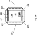
- the figure 1b presents the antenna of the figure la in its folded form. As can be seen from this example of the figure 1b Folding is antagonistic.
- the circuit board is folded for example at forty-five degrees, four times, (according to the dashed lines 105 of FIG. , which define the folding zones) alternately right then left, so that, during folding, the copper strip is not in contact with itself.
- the folding, according to the present technique can be a folding flat, as previously exposed or an intermediate folding, which can then be considered a deformation more than a real folding.
- An antenna is thus obtained, the characteristics of which are the same as with a "hollowed out" flexible printed circuit, but with a much lower cost of realization, precisely because it is not necessary to pay for the hollow part of the hose.
- the flexible printed circuit comprises two superimposed ends 110, 120. These zones are connected together during the binding, to allow the creation of the loops (or loops when there are several tracks).
- One of these superimposed ends may comprise fastening means (123), such as weld holes, to allow the antenna to be held in the folded position.
- Conductive glue dots may also be used.
- the general principle is to have a flexible printed circuit of longitudinal shape, comprising at least one copper track (the number of copper tracks represents the number of turns of the antenna), the flexible printed circuit comprising at least at least one folding zone shaped to allow the flexible printed circuit to pass from an unfolded state to a folded state in which the copper track forms at least one antenna loop.
- Folding the flexible printed circuit can be done either by hand or with the help of a suitable folder.
- the definition of the plane of the flexible printed circuit (that is to say of the unfolded form of the flexible printed circuit) takes into account, as the case may be, the folding zone or the loss at the bend. It is understood, as previously stated, that the folding is not necessarily a flat folding, but can also be a qualified partial folding or deformation.
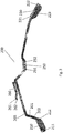
- the figure 2 illustrates a flex in unfolded position according to one embodiment of the invention.
- the flex 10 is drawn in length in an unfolded position and comprises two superimposed ends 210, 220, a central zone 250 and two lateral zones 230, 240.
- the two superposition zones 210, 120 and the central zone each comprise two orifices of 111, 112, 221, 222, 151, 152.
- One of the two superposition areas 210, 220 includes holes 223 for the soldering of the two superposition zones 210, 220.
- a connection extension 260 for connecting the antenna to a connector provided for this purpose on a motherboard, is disposed on one of the two lateral zones 130, 140.
- the figure 3 illustrates a flex according to a specific embodiment of the invention.
- the flexible printed circuit board 200 comprises three copper tracks 201, 202, 203. Holes 221, 222, 223 are disposed on the copper tracks in the superimposed end 220. The holes 221 and 222 are for attaching the antenna on the receiving part, in spaces provided for this purpose. The holes 223 are intended to allow welding of the two superposing zones 210 and 220.
- the connection extension 260 comprises two welding points 261, 262 that can be welded or plugged into a connector on the motherboard of the payment terminal.
- the flex in length allows to deduce the cost of material. Indeed, in the solution of the prior art, the flex is drawn in the form of a loop. The center of the loop is then dug to achieve the antenna. This excavated part always pays for the manufacturer. Thus, the flex in length in an unfolded position according to the invention makes it possible to avoid paying for the empty part of the solution of the prior art.
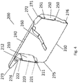
- the figure 4 illustrates a flex 200 in the folded position, which forms a contactless communication antenna in a payment terminal according to one embodiment of the invention.
- the flex in the folded position (antenna) is achieved by a folding operation or deformation of the unfolded flex position 100 illustrated in FIG. Figure 1 . This folding operation is performed on several folding zones 271, 272, 273, 274, 275, 276.
- the flex in the folded position comprises two superposed ends 210, 220, a central zone 250 and two lateral zones 230, 240.
- two superposition zones 210, 220 and the central zone each comprises two fixing holes 211, 212, 221, 222, 251, 252 making it possible to fix the antenna on the support piece in the payment terminal.
- the two fixing orifices 211, 212 on one end of superimposition 210 coincide respectively with the two fixing orifices 221, 222 on the other end of superimposition 220.
- One of the two superposing ends 210, 220 comprises holes (not shown) for welding the two superposition zones 210, 220.
- the figures 5 , 6 and 7 illustrate the closure of the flex loop when mounting the antenna on a support member, which in this embodiment is a paper roll housing 500.
- the two superimposed ends 210, 220 are superimposed and are fixed by welding. The welding is performed by positioning the holes 223 on the three copper tracks 201, 202, 203 in the overlapping end 220 which folds over and the beaches on the other overlapping end 210 which is located below.
- the ends of the copper tracks 201, 203 and 203 in the superimposed end 220 are respectively welded to the other ends of the tracks 203, 201 and 202 on the superimposing end 210, through holes 223.
- Such a weld allows both closing the flex loop 200, and also connecting the three copper tracks 201, 203, 203 to define the number of loops of the antenna (in this case three in this embodiment).
- the superposition of the two ends is defined so that the track 201 is welded with the track 202, which is itself welded with the track 203: this gives, at the end of the welding operation, a single conductive track, forming three turns around the support part (the housing 500).
- Fixing holes 221, 222 on the overlap end 220 are respectively superimposed on the fastening holes 211, 212 on the superimposing end 210, and form two superimposed fastening holes.
- the shape of the folded flex 200 adapts to the external shape of the housing 500.
- two fastening means 501, 502 (studs, clips) disposed on the housing 500 pass through the two superposed fixing holes.
- two fixing means 503, 504 pass through the two fixing orifices 251, 252 disposed on the central zone 250 of the flex.
- the diameter of the fastening means 501, 502, 503, 504 is greater than or equal to that of the fastening holes 211, 212, 221, 222, 251, 252, and allows the fixing means to maintain the flex while maintaining the ease of assembly of the flex.
- the two welding points 261, 262 are soldered to the motherboard of the payment terminal. The antenna thus becomes operational for receiving and transmitting signals.
- the two superimposed ends 210, 220 are superimposed and folded in an area on a PCB and fixed thereto with a connector through fixing holes 211, 212, 221, 222.
- the two however, the superimposing ends 210, 220 may be positioned without being superimposed in an area on the PCB and secured thereto with two connectors through fastening holes 211, 212, 221, 222.
- the flex in the folded position comprises two ends which are superimposed on a foldback zone. Closing the loop is achieved by stapling or crimping the two superposed ends.
Landscapes
- Engineering & Computer Science (AREA)
- Microelectronics & Electronic Packaging (AREA)
- Details Of Aerials (AREA)
Claims (6)
- Flexible Leiterplatte (10, 200) von länglicher Form, umfassend mindestens eine Leiterbahn (101, 201, 202, 203), die sich über die Länge der flexiblen Leiterplatte erstreckt, wobei die flexible Leiterplatte mindestens einen Faltbereich aufweist 105, 205), der ausgebildet ist, um den Übergang der flexiblen Leiterplatte von einem entfalteten Zustand in einen gefalteten Zustand zu ermöglichen, in dem die Leiterbahn mindestens eine Antennenschleife bildet, dadurch gekennzeichnet, dass sie aufweist:- mindestens zwei Leiterbahnen (201, 202, 203), die sich über die Länge der flexiblen Leiterplatte erstrecken, wobei die mindestens zwei Leiterbahnen (201, 202, 203) im Wesentlichen parallel zueinander sind,- mindestens einen Überlappungsbereich (110, 120, 210, 220) eines ersten Endes der Leiterplatte auf einem zweiten Ende der Leiterplatte.
- Flexible Leiterplatte (10, 200) nach Anspruch 1, dadurch gekennzeichnet, dass der Überlappungsbereich Mittel zum Verbinden (223) der mindestens zwei Leiterbahnen untereinander aufweist, um eine vorbestimmte Anzahl an Antennenschleifen zu bilden.
- Flexible Leiterplatte nach Anspruch 1, dadurch gekennzeichnet, dass sie eine Erweiterung der Verbindung (160, 260) der flexiblen Leiterplatte auf einem geeigneten Steckverbinder aufweist.
- Flexible Leiterplatte nach Anspruch 1, dadurch gekennzeichnet, dass sie mindestens ein Befestigungsloch (211, 212, 221, 222, 251, 252) der flexiblen Leiterplatte auf mindestens einem Antennenträger aufweist.
- Vorrichtung, umfassend drahtlose Kommunikationsmittel, die einen Sender-Empfänger und eine Antenne einsetzen, Vorrichtung, die dadurch gekennzeichnet ist, dass die Antenne eine flexible Leiterplatte nach einem der Ansprüche 1 bis 4 aufweist.
- Vorrichtung nach Anspruch 5, dadurch gekennzeichnet, dass das sie mindestens ein Trägerteil (500) aufweist, auf dem die Antenne angeordnet ist.
Priority Applications (1)
| Application Number | Priority Date | Filing Date | Title |
|---|---|---|---|
| PL16174869T PL3107149T3 (pl) | 2015-06-16 | 2016-06-16 | Elastyczny obwód drukowany zawierający bezprzewodową antenę komunikacyjną oraz urządzenie do terminala płatniczego zawierające taki elastyczny obwód drukowany |
Applications Claiming Priority (1)
| Application Number | Priority Date | Filing Date | Title |
|---|---|---|---|
| FR1555517A FR3037693B1 (fr) | 2015-06-16 | 2015-06-16 | Antenne de communication sans contact pour terminal de paiement |
Publications (2)
| Publication Number | Publication Date |
|---|---|
| EP3107149A1 EP3107149A1 (de) | 2016-12-21 |
| EP3107149B1 true EP3107149B1 (de) | 2018-09-05 |
Family
ID=54478109
Family Applications (1)
| Application Number | Title | Priority Date | Filing Date |
|---|---|---|---|
| EP16174869.4A Active EP3107149B1 (de) | 2015-06-16 | 2016-06-16 | Flexible gedruckte leiterplatte umfassend einer kontaktlosen kommunikationsantenne und baugruppe für zahlungsterminal umfassend solch einer flexiblen gedruckten leiterplatte |
Country Status (6)
| Country | Link |
|---|---|
| US (1) | US10446932B2 (de) |
| EP (1) | EP3107149B1 (de) |
| CA (1) | CA2933263C (de) |
| ES (1) | ES2700651T3 (de) |
| FR (1) | FR3037693B1 (de) |
| PL (1) | PL3107149T3 (de) |
Families Citing this family (6)
| Publication number | Priority date | Publication date | Assignee | Title |
|---|---|---|---|---|
| CN108511899B (zh) * | 2018-04-02 | 2020-02-14 | Oppo广东移动通信有限公司 | 印刷天线组件的制作方法、印刷天线组件及电子设备 |
| FR3092204B1 (fr) | 2019-01-29 | 2021-09-24 | Ingenico Group | Antenne de communication sans contact pour terminal de communication |
| WO2021000171A1 (zh) * | 2019-06-30 | 2021-01-07 | 瑞声声学科技(深圳)有限公司 | 传输线模组以及移动终端 |
| USD971899S1 (en) * | 2020-12-01 | 2022-12-06 | Field Theory Consulting Inc. | Radio-frequency antenna |
| USD971897S1 (en) * | 2020-12-01 | 2022-12-06 | Field Theory Consulting Inc. | Radio-frequency antenna |
| USD971898S1 (en) * | 2020-12-01 | 2022-12-06 | Field Theory Consulting Inc. | Radio-frequency antenna |
Family Cites Families (19)
| Publication number | Priority date | Publication date | Assignee | Title |
|---|---|---|---|---|
| US5285191A (en) * | 1981-10-30 | 1994-02-08 | Reeb Max E | LC marker construction useful as an electromagnetically interrogatable transponder means |
| US4755783A (en) * | 1986-11-18 | 1988-07-05 | Rogers Corporation | Inductive devices for printed wiring boards |
| EP0408588A4 (en) * | 1988-03-11 | 1991-08-21 | Magellan Corporation (Australia) Pty. Ltd. | Inductive element and method of manufacture |
| JPH069165U (ja) * | 1992-07-08 | 1994-02-04 | 旭光学工業株式会社 | フレキシブルプリント基板 |
| DE4433701A1 (de) * | 1994-09-21 | 1996-03-28 | Siemens Ag | Vorrichtung zur berührungslosen Energie- und Datenübertragung auf induktivem Wege, und bevorzugte Verwendung derselben zur Identifikation von Gasflaschen |
| WO2002003764A1 (en) * | 2000-06-30 | 2002-01-10 | Sanyo Electric Co., Ltd. | Flexible printed circuit board and foldable cell phone terminal |
| US6593900B1 (en) * | 2002-03-04 | 2003-07-15 | West Virginia University | Flexible printed circuit board antenna |
| DE202004007207U1 (de) * | 2004-04-30 | 2004-12-09 | Würth Elektronik Rot am See GmbH & Co. KG | Schaltungsträger |
| DE102005016676B4 (de) * | 2005-04-12 | 2009-09-17 | Carl Freudenberg Kg | Leiterbahn für elektronische Zwecke |
| CN101233533B (zh) * | 2005-08-03 | 2011-02-16 | 松下电器产业株式会社 | 天线内置型存储媒介物 |
| TWI289372B (en) * | 2005-09-30 | 2007-11-01 | Adv Flexible Circuits Co Ltd | Stackable assembly signal flat cable |
| WO2007042963A1 (en) * | 2005-10-13 | 2007-04-19 | Nxp B.V. | Electronic device or circuit and method for fabricating the same |
| JP2007305656A (ja) * | 2006-05-09 | 2007-11-22 | Sumitomo Bakelite Co Ltd | コイル部材 |
| TW201043103A (en) * | 2009-05-22 | 2010-12-01 | Adv Flexible Circuits Co Ltd | Flexible circuit cable with cluster sections |
| JP5455034B2 (ja) * | 2009-12-09 | 2014-03-26 | ホシデン株式会社 | フレキシブル配線基板 |
| US8543190B2 (en) * | 2010-07-30 | 2013-09-24 | Medtronic, Inc. | Inductive coil device on flexible substrate |
| US8973252B2 (en) * | 2012-09-27 | 2015-03-10 | Toyota Motor Engineering & Manufacturing North America, Inc. | Folded planar Litz wire and method of making same |
| JP5839236B2 (ja) * | 2012-10-16 | 2016-01-06 | カシオ計算機株式会社 | 携帯端末 |
| US9583256B2 (en) * | 2014-06-13 | 2017-02-28 | Verily Life Sciences Llc | Three-dimensional wireless charging coil |
-
2015
- 2015-06-16 FR FR1555517A patent/FR3037693B1/fr not_active Expired - Fee Related
-
2016
- 2016-06-16 EP EP16174869.4A patent/EP3107149B1/de active Active
- 2016-06-16 CA CA2933263A patent/CA2933263C/en active Active
- 2016-06-16 PL PL16174869T patent/PL3107149T3/pl unknown
- 2016-06-16 US US15/184,148 patent/US10446932B2/en active Active
- 2016-06-16 ES ES16174869T patent/ES2700651T3/es active Active
Also Published As
| Publication number | Publication date |
|---|---|
| EP3107149A1 (de) | 2016-12-21 |
| PL3107149T3 (pl) | 2019-02-28 |
| FR3037693A1 (fr) | 2016-12-23 |
| US10446932B2 (en) | 2019-10-15 |
| US20160372829A1 (en) | 2016-12-22 |
| CA2933263C (en) | 2023-09-19 |
| CA2933263A1 (en) | 2016-12-16 |
| FR3037693B1 (fr) | 2018-07-13 |
| ES2700651T3 (es) | 2019-02-18 |
Similar Documents
| Publication | Publication Date | Title |
|---|---|---|
| EP3107149A1 (de) | Flexible gedruckte leiterplatte umfassend einer kontaktlosen kommunikationsantenne und baugruppe für zahlungsterminal umfassend solch einer flexiblen gedruckten leiterplatte | |
| CA2752609C (fr) | Carte nfc pour dispositif portatif | |
| EP2801058B1 (de) | Verfahren zur kommunikation zwischen einer nfc karte mit doppelkontakt- und kontaktloser schnittstelle in einem nfc-endgerät und einer nfc-vorrichtung | |
| CA2746241C (fr) | Circuit d'antenne rfid | |
| EP2174269B1 (de) | Gesichertes dokument mit kontaktlosem chip und schutz von daten gegen unautorisierten zugriff | |
| US12212047B2 (en) | Automatically reconfigurable antenna circuit for enabling operation within multiple frequency bands | |
| CN207301665U (zh) | 电子设备 | |
| US20140184461A1 (en) | Antenna Assembly | |
| EP3918667B1 (de) | Kontaktlose kommunikationsantenne für kommunikationsendgerät | |
| EP3427189B1 (de) | Fingergesteuerte kontaktlose chipkarte | |
| EP3391460B1 (de) | Einseitiges antennenmodul mit cms-komponenten | |
| WO2010060956A1 (fr) | Circuit électrique / électronique pour connecter un dispositif à une antenne radiofréquence | |
| FR3144354A1 (fr) | Carte à puce avec antennes radiofréquences | |
| EP3029766B1 (de) | Kontaktlose antenne, halterungsstruktur und entsprechender anschluss | |
| EP4478246A1 (de) | Chipkarte mit funkfrequenzantennen | |
| EP2471030B1 (de) | Vorrichtung mit einer relais-antenne, zugehörige radiofrequenzvorrichtung und zugehöriges verfahren | |
| FR2965084A1 (fr) | Carte nfc pour dispositif portatif | |
| EP2431927A1 (de) | Wirbelstromempfindliche NFC Karte |
Legal Events
| Date | Code | Title | Description |
|---|---|---|---|
| PUAI | Public reference made under article 153(3) epc to a published international application that has entered the european phase |
Free format text: ORIGINAL CODE: 0009012 |
|
| STAA | Information on the status of an ep patent application or granted ep patent |
Free format text: STATUS: THE APPLICATION HAS BEEN PUBLISHED |
|
| AK | Designated contracting states |
Kind code of ref document: A1 Designated state(s): AL AT BE BG CH CY CZ DE DK EE ES FI FR GB GR HR HU IE IS IT LI LT LU LV MC MK MT NL NO PL PT RO RS SE SI SK SM TR |
|
| AX | Request for extension of the european patent |
Extension state: BA ME |
|
| STAA | Information on the status of an ep patent application or granted ep patent |
Free format text: STATUS: REQUEST FOR EXAMINATION WAS MADE |
|
| 17P | Request for examination filed |
Effective date: 20170320 |
|
| RBV | Designated contracting states (corrected) |
Designated state(s): AL AT BE BG CH CY CZ DE DK EE ES FI FR GB GR HR HU IE IS IT LI LT LU LV MC MK MT NL NO PL PT RO RS SE SI SK SM TR |
|
| GRAP | Despatch of communication of intention to grant a patent |
Free format text: ORIGINAL CODE: EPIDOSNIGR1 |
|
| RIC1 | Information provided on ipc code assigned before grant |
Ipc: H05K 1/02 20060101ALI20180221BHEP Ipc: H01Q 1/38 20060101AFI20180221BHEP Ipc: H04B 5/00 20060101ALN20180221BHEP Ipc: H05K 1/16 20060101ALN20180221BHEP Ipc: H01Q 7/02 20060101ALI20180221BHEP |
|
| STAA | Information on the status of an ep patent application or granted ep patent |
Free format text: STATUS: GRANT OF PATENT IS INTENDED |
|
| INTG | Intention to grant announced |
Effective date: 20180329 |
|
| GRAS | Grant fee paid |
Free format text: ORIGINAL CODE: EPIDOSNIGR3 |
|
| GRAA | (expected) grant |
Free format text: ORIGINAL CODE: 0009210 |
|
| STAA | Information on the status of an ep patent application or granted ep patent |
Free format text: STATUS: THE PATENT HAS BEEN GRANTED |
|
| AK | Designated contracting states |
Kind code of ref document: B1 Designated state(s): AL AT BE BG CH CY CZ DE DK EE ES FI FR GB GR HR HU IE IS IT LI LT LU LV MC MK MT NL NO PL PT RO RS SE SI SK SM TR |
|
| REG | Reference to a national code |
Ref country code: GB Ref legal event code: FG4D Free format text: NOT ENGLISH |
|
| REG | Reference to a national code |
Ref country code: CH Ref legal event code: EP |
|
| REG | Reference to a national code |
Ref country code: AT Ref legal event code: REF Ref document number: 1038929 Country of ref document: AT Kind code of ref document: T Effective date: 20180915 |
|
| REG | Reference to a national code |
Ref country code: DE Ref legal event code: R096 Ref document number: 602016005288 Country of ref document: DE |
|
| REG | Reference to a national code |
Ref country code: IE Ref legal event code: FG4D Free format text: LANGUAGE OF EP DOCUMENT: FRENCH |
|
| REG | Reference to a national code |
Ref country code: NL Ref legal event code: MP Effective date: 20180905 |
|
| REG | Reference to a national code |
Ref country code: LT Ref legal event code: MG4D |
|
| PG25 | Lapsed in a contracting state [announced via postgrant information from national office to epo] |
Ref country code: RS Free format text: LAPSE BECAUSE OF FAILURE TO SUBMIT A TRANSLATION OF THE DESCRIPTION OR TO PAY THE FEE WITHIN THE PRESCRIBED TIME-LIMIT Effective date: 20180905 Ref country code: LT Free format text: LAPSE BECAUSE OF FAILURE TO SUBMIT A TRANSLATION OF THE DESCRIPTION OR TO PAY THE FEE WITHIN THE PRESCRIBED TIME-LIMIT Effective date: 20180905 Ref country code: BG Free format text: LAPSE BECAUSE OF FAILURE TO SUBMIT A TRANSLATION OF THE DESCRIPTION OR TO PAY THE FEE WITHIN THE PRESCRIBED TIME-LIMIT Effective date: 20181205 Ref country code: SE Free format text: LAPSE BECAUSE OF FAILURE TO SUBMIT A TRANSLATION OF THE DESCRIPTION OR TO PAY THE FEE WITHIN THE PRESCRIBED TIME-LIMIT Effective date: 20180905 Ref country code: FI Free format text: LAPSE BECAUSE OF FAILURE TO SUBMIT A TRANSLATION OF THE DESCRIPTION OR TO PAY THE FEE WITHIN THE PRESCRIBED TIME-LIMIT Effective date: 20180905 Ref country code: NO Free format text: LAPSE BECAUSE OF FAILURE TO SUBMIT A TRANSLATION OF THE DESCRIPTION OR TO PAY THE FEE WITHIN THE PRESCRIBED TIME-LIMIT Effective date: 20181205 |
|
| REG | Reference to a national code |
Ref country code: AT Ref legal event code: MK05 Ref document number: 1038929 Country of ref document: AT Kind code of ref document: T Effective date: 20180905 |
|
| REG | Reference to a national code |
Ref country code: ES Ref legal event code: FG2A Ref document number: 2700651 Country of ref document: ES Kind code of ref document: T3 Effective date: 20190218 |
|
| PG25 | Lapsed in a contracting state [announced via postgrant information from national office to epo] |
Ref country code: LV Free format text: LAPSE BECAUSE OF FAILURE TO SUBMIT A TRANSLATION OF THE DESCRIPTION OR TO PAY THE FEE WITHIN THE PRESCRIBED TIME-LIMIT Effective date: 20180905 Ref country code: HR Free format text: LAPSE BECAUSE OF FAILURE TO SUBMIT A TRANSLATION OF THE DESCRIPTION OR TO PAY THE FEE WITHIN THE PRESCRIBED TIME-LIMIT Effective date: 20180905 Ref country code: AL Free format text: LAPSE BECAUSE OF FAILURE TO SUBMIT A TRANSLATION OF THE DESCRIPTION OR TO PAY THE FEE WITHIN THE PRESCRIBED TIME-LIMIT Effective date: 20180905 |
|
| REG | Reference to a national code |
Ref country code: GR Ref legal event code: EP Ref document number: 20180403546 Country of ref document: GR Effective date: 20190404 |
|
| PG25 | Lapsed in a contracting state [announced via postgrant information from national office to epo] |
Ref country code: RO Free format text: LAPSE BECAUSE OF FAILURE TO SUBMIT A TRANSLATION OF THE DESCRIPTION OR TO PAY THE FEE WITHIN THE PRESCRIBED TIME-LIMIT Effective date: 20180905 Ref country code: CZ Free format text: LAPSE BECAUSE OF FAILURE TO SUBMIT A TRANSLATION OF THE DESCRIPTION OR TO PAY THE FEE WITHIN THE PRESCRIBED TIME-LIMIT Effective date: 20180905 Ref country code: IS Free format text: LAPSE BECAUSE OF FAILURE TO SUBMIT A TRANSLATION OF THE DESCRIPTION OR TO PAY THE FEE WITHIN THE PRESCRIBED TIME-LIMIT Effective date: 20190105 Ref country code: NL Free format text: LAPSE BECAUSE OF FAILURE TO SUBMIT A TRANSLATION OF THE DESCRIPTION OR TO PAY THE FEE WITHIN THE PRESCRIBED TIME-LIMIT Effective date: 20180905 Ref country code: EE Free format text: LAPSE BECAUSE OF FAILURE TO SUBMIT A TRANSLATION OF THE DESCRIPTION OR TO PAY THE FEE WITHIN THE PRESCRIBED TIME-LIMIT Effective date: 20180905 Ref country code: AT Free format text: LAPSE BECAUSE OF FAILURE TO SUBMIT A TRANSLATION OF THE DESCRIPTION OR TO PAY THE FEE WITHIN THE PRESCRIBED TIME-LIMIT Effective date: 20180905 |
|
| PG25 | Lapsed in a contracting state [announced via postgrant information from national office to epo] |
Ref country code: SM Free format text: LAPSE BECAUSE OF FAILURE TO SUBMIT A TRANSLATION OF THE DESCRIPTION OR TO PAY THE FEE WITHIN THE PRESCRIBED TIME-LIMIT Effective date: 20180905 Ref country code: SK Free format text: LAPSE BECAUSE OF FAILURE TO SUBMIT A TRANSLATION OF THE DESCRIPTION OR TO PAY THE FEE WITHIN THE PRESCRIBED TIME-LIMIT Effective date: 20180905 Ref country code: PT Free format text: LAPSE BECAUSE OF FAILURE TO SUBMIT A TRANSLATION OF THE DESCRIPTION OR TO PAY THE FEE WITHIN THE PRESCRIBED TIME-LIMIT Effective date: 20190105 |
|
| REG | Reference to a national code |
Ref country code: DE Ref legal event code: R097 Ref document number: 602016005288 Country of ref document: DE |
|
| PLBE | No opposition filed within time limit |
Free format text: ORIGINAL CODE: 0009261 |
|
| STAA | Information on the status of an ep patent application or granted ep patent |
Free format text: STATUS: NO OPPOSITION FILED WITHIN TIME LIMIT |
|
| PG25 | Lapsed in a contracting state [announced via postgrant information from national office to epo] |
Ref country code: DK Free format text: LAPSE BECAUSE OF FAILURE TO SUBMIT A TRANSLATION OF THE DESCRIPTION OR TO PAY THE FEE WITHIN THE PRESCRIBED TIME-LIMIT Effective date: 20180905 |
|
| 26N | No opposition filed |
Effective date: 20190606 |
|
| PG25 | Lapsed in a contracting state [announced via postgrant information from national office to epo] |
Ref country code: SI Free format text: LAPSE BECAUSE OF FAILURE TO SUBMIT A TRANSLATION OF THE DESCRIPTION OR TO PAY THE FEE WITHIN THE PRESCRIBED TIME-LIMIT Effective date: 20180905 |
|
| PG25 | Lapsed in a contracting state [announced via postgrant information from national office to epo] |
Ref country code: MC Free format text: LAPSE BECAUSE OF FAILURE TO SUBMIT A TRANSLATION OF THE DESCRIPTION OR TO PAY THE FEE WITHIN THE PRESCRIBED TIME-LIMIT Effective date: 20180905 |
|
| REG | Reference to a national code |
Ref country code: CH Ref legal event code: PL |
|
| REG | Reference to a national code |
Ref country code: BE Ref legal event code: MM Effective date: 20190630 |
|
| PG25 | Lapsed in a contracting state [announced via postgrant information from national office to epo] |
Ref country code: TR Free format text: LAPSE BECAUSE OF FAILURE TO SUBMIT A TRANSLATION OF THE DESCRIPTION OR TO PAY THE FEE WITHIN THE PRESCRIBED TIME-LIMIT Effective date: 20180905 |
|
| PG25 | Lapsed in a contracting state [announced via postgrant information from national office to epo] |
Ref country code: IE Free format text: LAPSE BECAUSE OF NON-PAYMENT OF DUE FEES Effective date: 20190616 |
|
| PG25 | Lapsed in a contracting state [announced via postgrant information from national office to epo] |
Ref country code: LI Free format text: LAPSE BECAUSE OF NON-PAYMENT OF DUE FEES Effective date: 20190630 Ref country code: LU Free format text: LAPSE BECAUSE OF NON-PAYMENT OF DUE FEES Effective date: 20190616 Ref country code: BE Free format text: LAPSE BECAUSE OF NON-PAYMENT OF DUE FEES Effective date: 20190630 Ref country code: CH Free format text: LAPSE BECAUSE OF NON-PAYMENT OF DUE FEES Effective date: 20190630 |
|
| PG25 | Lapsed in a contracting state [announced via postgrant information from national office to epo] |
Ref country code: CY Free format text: LAPSE BECAUSE OF FAILURE TO SUBMIT A TRANSLATION OF THE DESCRIPTION OR TO PAY THE FEE WITHIN THE PRESCRIBED TIME-LIMIT Effective date: 20180905 |
|
| PG25 | Lapsed in a contracting state [announced via postgrant information from national office to epo] |
Ref country code: HU Free format text: LAPSE BECAUSE OF FAILURE TO SUBMIT A TRANSLATION OF THE DESCRIPTION OR TO PAY THE FEE WITHIN THE PRESCRIBED TIME-LIMIT; INVALID AB INITIO Effective date: 20160616 Ref country code: MT Free format text: LAPSE BECAUSE OF FAILURE TO SUBMIT A TRANSLATION OF THE DESCRIPTION OR TO PAY THE FEE WITHIN THE PRESCRIBED TIME-LIMIT Effective date: 20180905 |
|
| REG | Reference to a national code |
Ref country code: GB Ref legal event code: 732E Free format text: REGISTERED BETWEEN 20220127 AND 20220202 |
|
| PG25 | Lapsed in a contracting state [announced via postgrant information from national office to epo] |
Ref country code: MK Free format text: LAPSE BECAUSE OF FAILURE TO SUBMIT A TRANSLATION OF THE DESCRIPTION OR TO PAY THE FEE WITHIN THE PRESCRIBED TIME-LIMIT Effective date: 20180905 |
|
| REG | Reference to a national code |
Ref country code: DE Ref legal event code: R081 Ref document number: 602016005288 Country of ref document: DE Owner name: BANKS AND ACQUIRES INTERNATIONAL HOLDING, FR Free format text: FORMER OWNER: INGENICO GROUP, PARIS, FR Ref country code: DE Ref legal event code: R082 Ref document number: 602016005288 Country of ref document: DE Representative=s name: STUMPF PATENTANWAELTE PARTGMBB, DE Ref country code: DE Ref legal event code: R081 Ref document number: 602016005288 Country of ref document: DE Owner name: BANKS AND ACQUIRERS INTERNATIONAL HOLDING, FR Free format text: FORMER OWNER: INGENICO GROUP, PARIS, FR |
|
| REG | Reference to a national code |
Ref country code: DE Ref legal event code: R081 Ref document number: 602016005288 Country of ref document: DE Owner name: BANKS AND ACQUIRERS INTERNATIONAL HOLDING, FR Free format text: FORMER OWNER: BANKS AND ACQUIRES INTERNATIONAL HOLDING, SURESNES, FR |
|
| PGFP | Annual fee paid to national office [announced via postgrant information from national office to epo] |
Ref country code: PL Payment date: 20250522 Year of fee payment: 10 Ref country code: DE Payment date: 20250618 Year of fee payment: 10 |
|
| PGFP | Annual fee paid to national office [announced via postgrant information from national office to epo] |
Ref country code: GB Payment date: 20250618 Year of fee payment: 10 |
|
| PGFP | Annual fee paid to national office [announced via postgrant information from national office to epo] |
Ref country code: FR Payment date: 20250627 Year of fee payment: 10 |
|
| PGFP | Annual fee paid to national office [announced via postgrant information from national office to epo] |
Ref country code: GR Payment date: 20250620 Year of fee payment: 10 |
|
| REG | Reference to a national code |
Ref country code: ES Ref legal event code: PC2A Owner name: BANKS AND ACQUIRERS INTERNATIONAL HOLDING Effective date: 20250929 |
|
| PGFP | Annual fee paid to national office [announced via postgrant information from national office to epo] |
Ref country code: ES Payment date: 20250728 Year of fee payment: 10 |
|
| PGFP | Annual fee paid to national office [announced via postgrant information from national office to epo] |
Ref country code: IT Payment date: 20250624 Year of fee payment: 10 |
|
| P01 | Opt-out of the competence of the unified patent court (upc) registered |
Free format text: CASE NUMBER: UPC_APP_0000325_3107149/2026 Effective date: 20260106 |