EP3104400A1 - Electronic component module, and manufacturing method of electronic component module - Google Patents
Electronic component module, and manufacturing method of electronic component module Download PDFInfo
- Publication number
- EP3104400A1 EP3104400A1 EP15746474.4A EP15746474A EP3104400A1 EP 3104400 A1 EP3104400 A1 EP 3104400A1 EP 15746474 A EP15746474 A EP 15746474A EP 3104400 A1 EP3104400 A1 EP 3104400A1
- Authority
- EP
- European Patent Office
- Prior art keywords
- copper
- electronic component
- component module
- sintered
- copper particles
- Prior art date
- Legal status (The legal status is an assumption and is not a legal conclusion. Google has not performed a legal analysis and makes no representation as to the accuracy of the status listed.)
- Granted
Links
Images






Classifications
-
- H—ELECTRICITY
- H01—ELECTRIC ELEMENTS
- H01B—CABLES; CONDUCTORS; INSULATORS; SELECTION OF MATERIALS FOR THEIR CONDUCTIVE, INSULATING OR DIELECTRIC PROPERTIES
- H01B1/00—Conductors or conductive bodies characterised by the conductive materials; Selection of materials as conductors
- H01B1/20—Conductive material dispersed in non-conductive organic material
- H01B1/22—Conductive material dispersed in non-conductive organic material the conductive material comprising metals or alloys
-
- B—PERFORMING OPERATIONS; TRANSPORTING
- B22—CASTING; POWDER METALLURGY
- B22F—WORKING METALLIC POWDER; MANUFACTURE OF ARTICLES FROM METALLIC POWDER; MAKING METALLIC POWDER; APPARATUS OR DEVICES SPECIALLY ADAPTED FOR METALLIC POWDER
- B22F1/00—Metallic powder; Treatment of metallic powder, e.g. to facilitate working or to improve properties
- B22F1/10—Metallic powder containing lubricating or binding agents; Metallic powder containing organic material
-
- B—PERFORMING OPERATIONS; TRANSPORTING
- B22—CASTING; POWDER METALLURGY
- B22F—WORKING METALLIC POWDER; MANUFACTURE OF ARTICLES FROM METALLIC POWDER; MAKING METALLIC POWDER; APPARATUS OR DEVICES SPECIALLY ADAPTED FOR METALLIC POWDER
- B22F7/00—Manufacture of composite layers, workpieces, or articles, comprising metallic powder, by sintering the powder, with or without compacting wherein at least one part is obtained by sintering or compression
- B22F7/06—Manufacture of composite layers, workpieces, or articles, comprising metallic powder, by sintering the powder, with or without compacting wherein at least one part is obtained by sintering or compression of composite workpieces or articles from parts, e.g. to form tipped tools
- B22F7/062—Manufacture of composite layers, workpieces, or articles, comprising metallic powder, by sintering the powder, with or without compacting wherein at least one part is obtained by sintering or compression of composite workpieces or articles from parts, e.g. to form tipped tools involving the connection or repairing of preformed parts
- B22F7/064—Manufacture of composite layers, workpieces, or articles, comprising metallic powder, by sintering the powder, with or without compacting wherein at least one part is obtained by sintering or compression of composite workpieces or articles from parts, e.g. to form tipped tools involving the connection or repairing of preformed parts using an intermediate powder layer
-
- H—ELECTRICITY
- H05—ELECTRIC TECHNIQUES NOT OTHERWISE PROVIDED FOR
- H05K—PRINTED CIRCUITS; CASINGS OR CONSTRUCTIONAL DETAILS OF ELECTRIC APPARATUS; MANUFACTURE OF ASSEMBLAGES OF ELECTRICAL COMPONENTS
- H05K1/00—Printed circuits
- H05K1/02—Details
- H05K1/09—Use of materials for the conductive, e.g. metallic pattern
- H05K1/092—Dispersed materials, e.g. conductive pastes or inks
- H05K1/097—Inks comprising nanoparticles and specially adapted for being sintered at low temperature
-
- H—ELECTRICITY
- H05—ELECTRIC TECHNIQUES NOT OTHERWISE PROVIDED FOR
- H05K—PRINTED CIRCUITS; CASINGS OR CONSTRUCTIONAL DETAILS OF ELECTRIC APPARATUS; MANUFACTURE OF ASSEMBLAGES OF ELECTRICAL COMPONENTS
- H05K1/00—Printed circuits
- H05K1/18—Printed circuits structurally associated with non-printed electric components
- H05K1/181—Printed circuits structurally associated with non-printed electric components associated with surface mounted components
-
- H—ELECTRICITY
- H05—ELECTRIC TECHNIQUES NOT OTHERWISE PROVIDED FOR
- H05K—PRINTED CIRCUITS; CASINGS OR CONSTRUCTIONAL DETAILS OF ELECTRIC APPARATUS; MANUFACTURE OF ASSEMBLAGES OF ELECTRICAL COMPONENTS
- H05K3/00—Apparatus or processes for manufacturing printed circuits
- H05K3/30—Assembling printed circuits with electric components, e.g. with resistors
- H05K3/32—Assembling printed circuits with electric components, e.g. with resistors electrically connecting electric components or wires to printed circuits
-
- H—ELECTRICITY
- H10—SEMICONDUCTOR DEVICES; ELECTRIC SOLID-STATE DEVICES NOT OTHERWISE PROVIDED FOR
- H10W—GENERIC PACKAGES, INTERCONNECTIONS, CONNECTORS OR OTHER CONSTRUCTIONAL DETAILS OF DEVICES COVERED BY CLASS H10
- H10W72/00—Interconnections or connectors in packages
- H10W72/20—Bump connectors, e.g. solder bumps or copper pillars; Dummy bumps; Thermal bumps
-
- B—PERFORMING OPERATIONS; TRANSPORTING
- B23—MACHINE TOOLS; METAL-WORKING NOT OTHERWISE PROVIDED FOR
- B23K—SOLDERING OR UNSOLDERING; WELDING; CLADDING OR PLATING BY SOLDERING OR WELDING; CUTTING BY APPLYING HEAT LOCALLY, e.g. FLAME CUTTING; WORKING BY LASER BEAM
- B23K35/00—Rods, electrodes, materials, or media, for use in soldering, welding, or cutting
- B23K35/02—Rods, electrodes, materials, or media, for use in soldering, welding, or cutting characterised by mechanical features, e.g. shape
- B23K35/0222—Rods, electrodes, materials, or media, for use in soldering, welding, or cutting characterised by mechanical features, e.g. shape for use in soldering or brazing
- B23K35/0244—Powders, particles or spheres; Preforms made therefrom
- B23K35/025—Pastes, creams or slurries
-
- B—PERFORMING OPERATIONS; TRANSPORTING
- B23—MACHINE TOOLS; METAL-WORKING NOT OTHERWISE PROVIDED FOR
- B23K—SOLDERING OR UNSOLDERING; WELDING; CLADDING OR PLATING BY SOLDERING OR WELDING; CUTTING BY APPLYING HEAT LOCALLY, e.g. FLAME CUTTING; WORKING BY LASER BEAM
- B23K35/00—Rods, electrodes, materials, or media, for use in soldering, welding, or cutting
- B23K35/22—Rods, electrodes, materials, or media, for use in soldering, welding, or cutting characterised by the composition or nature of the material
- B23K35/24—Selection of soldering or welding materials proper
- B23K35/30—Selection of soldering or welding materials proper with the principal constituent melting at less than 1550°C
- B23K35/302—Cu as the principal constituent
-
- H—ELECTRICITY
- H05—ELECTRIC TECHNIQUES NOT OTHERWISE PROVIDED FOR
- H05K—PRINTED CIRCUITS; CASINGS OR CONSTRUCTIONAL DETAILS OF ELECTRIC APPARATUS; MANUFACTURE OF ASSEMBLAGES OF ELECTRICAL COMPONENTS
- H05K2201/00—Indexing scheme relating to printed circuits covered by H05K1/00
- H05K2201/02—Fillers; Particles; Fibers; Reinforcement materials
- H05K2201/0203—Fillers and particles
- H05K2201/0242—Shape of an individual particle
- H05K2201/0257—Nanoparticles
-
- H—ELECTRICITY
- H05—ELECTRIC TECHNIQUES NOT OTHERWISE PROVIDED FOR
- H05K—PRINTED CIRCUITS; CASINGS OR CONSTRUCTIONAL DETAILS OF ELECTRIC APPARATUS; MANUFACTURE OF ASSEMBLAGES OF ELECTRICAL COMPONENTS
- H05K2201/00—Indexing scheme relating to printed circuits covered by H05K1/00
- H05K2201/10—Details of components or other objects attached to or integrated in a printed circuit board
- H05K2201/10007—Types of components
- H05K2201/10015—Non-printed capacitor
-
- H—ELECTRICITY
- H05—ELECTRIC TECHNIQUES NOT OTHERWISE PROVIDED FOR
- H05K—PRINTED CIRCUITS; CASINGS OR CONSTRUCTIONAL DETAILS OF ELECTRIC APPARATUS; MANUFACTURE OF ASSEMBLAGES OF ELECTRICAL COMPONENTS
- H05K2203/00—Indexing scheme relating to apparatus or processes for manufacturing printed circuits covered by H05K3/00
- H05K2203/11—Treatments characterised by their effect, e.g. heating, cooling, roughening
- H05K2203/1131—Sintering, i.e. fusing of metal particles to achieve or improve electrical conductivity
-
- H—ELECTRICITY
- H10—SEMICONDUCTOR DEVICES; ELECTRIC SOLID-STATE DEVICES NOT OTHERWISE PROVIDED FOR
- H10W—GENERIC PACKAGES, INTERCONNECTIONS, CONNECTORS OR OTHER CONSTRUCTIONAL DETAILS OF DEVICES COVERED BY CLASS H10
- H10W72/00—Interconnections or connectors in packages
- H10W72/01—Manufacture or treatment
- H10W72/013—Manufacture or treatment of die-attach connectors
- H10W72/01321—Manufacture or treatment of die-attach connectors using local deposition
- H10W72/01323—Manufacture or treatment of die-attach connectors using local deposition in liquid form, e.g. by dispensing droplets or by screen printing
-
- H—ELECTRICITY
- H10—SEMICONDUCTOR DEVICES; ELECTRIC SOLID-STATE DEVICES NOT OTHERWISE PROVIDED FOR
- H10W—GENERIC PACKAGES, INTERCONNECTIONS, CONNECTORS OR OTHER CONSTRUCTIONAL DETAILS OF DEVICES COVERED BY CLASS H10
- H10W72/00—Interconnections or connectors in packages
- H10W72/01—Manufacture or treatment
- H10W72/016—Manufacture or treatment of strap connectors
-
- H—ELECTRICITY
- H10—SEMICONDUCTOR DEVICES; ELECTRIC SOLID-STATE DEVICES NOT OTHERWISE PROVIDED FOR
- H10W—GENERIC PACKAGES, INTERCONNECTIONS, CONNECTORS OR OTHER CONSTRUCTIONAL DETAILS OF DEVICES COVERED BY CLASS H10
- H10W72/00—Interconnections or connectors in packages
- H10W72/071—Connecting or disconnecting
- H10W72/072—Connecting or disconnecting of bump connectors
-
- H—ELECTRICITY
- H10—SEMICONDUCTOR DEVICES; ELECTRIC SOLID-STATE DEVICES NOT OTHERWISE PROVIDED FOR
- H10W—GENERIC PACKAGES, INTERCONNECTIONS, CONNECTORS OR OTHER CONSTRUCTIONAL DETAILS OF DEVICES COVERED BY CLASS H10
- H10W72/00—Interconnections or connectors in packages
- H10W72/071—Connecting or disconnecting
- H10W72/072—Connecting or disconnecting of bump connectors
- H10W72/07251—Connecting or disconnecting of bump connectors characterised by changes in properties of the bump connectors during connecting
- H10W72/07255—Connecting or disconnecting of bump connectors characterised by changes in properties of the bump connectors during connecting changes in materials
-
- H—ELECTRICITY
- H10—SEMICONDUCTOR DEVICES; ELECTRIC SOLID-STATE DEVICES NOT OTHERWISE PROVIDED FOR
- H10W—GENERIC PACKAGES, INTERCONNECTIONS, CONNECTORS OR OTHER CONSTRUCTIONAL DETAILS OF DEVICES COVERED BY CLASS H10
- H10W72/00—Interconnections or connectors in packages
- H10W72/071—Connecting or disconnecting
- H10W72/073—Connecting or disconnecting of die-attach connectors
- H10W72/07331—Connecting techniques
-
- H—ELECTRICITY
- H10—SEMICONDUCTOR DEVICES; ELECTRIC SOLID-STATE DEVICES NOT OTHERWISE PROVIDED FOR
- H10W—GENERIC PACKAGES, INTERCONNECTIONS, CONNECTORS OR OTHER CONSTRUCTIONAL DETAILS OF DEVICES COVERED BY CLASS H10
- H10W72/00—Interconnections or connectors in packages
- H10W72/071—Connecting or disconnecting
- H10W72/073—Connecting or disconnecting of die-attach connectors
- H10W72/07341—Controlling the bonding environment, e.g. atmosphere composition or temperature
-
- H—ELECTRICITY
- H10—SEMICONDUCTOR DEVICES; ELECTRIC SOLID-STATE DEVICES NOT OTHERWISE PROVIDED FOR
- H10W—GENERIC PACKAGES, INTERCONNECTIONS, CONNECTORS OR OTHER CONSTRUCTIONAL DETAILS OF DEVICES COVERED BY CLASS H10
- H10W72/00—Interconnections or connectors in packages
- H10W72/20—Bump connectors, e.g. solder bumps or copper pillars; Dummy bumps; Thermal bumps
- H10W72/221—Structures or relative sizes
- H10W72/225—Bumps having a filler embedded in a matrix
-
- H—ELECTRICITY
- H10—SEMICONDUCTOR DEVICES; ELECTRIC SOLID-STATE DEVICES NOT OTHERWISE PROVIDED FOR
- H10W—GENERIC PACKAGES, INTERCONNECTIONS, CONNECTORS OR OTHER CONSTRUCTIONAL DETAILS OF DEVICES COVERED BY CLASS H10
- H10W72/00—Interconnections or connectors in packages
- H10W72/20—Bump connectors, e.g. solder bumps or copper pillars; Dummy bumps; Thermal bumps
- H10W72/241—Dispositions, e.g. layouts
-
- H—ELECTRICITY
- H10—SEMICONDUCTOR DEVICES; ELECTRIC SOLID-STATE DEVICES NOT OTHERWISE PROVIDED FOR
- H10W—GENERIC PACKAGES, INTERCONNECTIONS, CONNECTORS OR OTHER CONSTRUCTIONAL DETAILS OF DEVICES COVERED BY CLASS H10
- H10W72/00—Interconnections or connectors in packages
- H10W72/20—Bump connectors, e.g. solder bumps or copper pillars; Dummy bumps; Thermal bumps
- H10W72/251—Materials
-
- H—ELECTRICITY
- H10—SEMICONDUCTOR DEVICES; ELECTRIC SOLID-STATE DEVICES NOT OTHERWISE PROVIDED FOR
- H10W—GENERIC PACKAGES, INTERCONNECTIONS, CONNECTORS OR OTHER CONSTRUCTIONAL DETAILS OF DEVICES COVERED BY CLASS H10
- H10W72/00—Interconnections or connectors in packages
- H10W72/20—Bump connectors, e.g. solder bumps or copper pillars; Dummy bumps; Thermal bumps
- H10W72/251—Materials
- H10W72/252—Materials comprising solid metals or solid metalloids, e.g. PbSn, Ag or Cu
-
- H—ELECTRICITY
- H10—SEMICONDUCTOR DEVICES; ELECTRIC SOLID-STATE DEVICES NOT OTHERWISE PROVIDED FOR
- H10W—GENERIC PACKAGES, INTERCONNECTIONS, CONNECTORS OR OTHER CONSTRUCTIONAL DETAILS OF DEVICES COVERED BY CLASS H10
- H10W72/00—Interconnections or connectors in packages
- H10W72/20—Bump connectors, e.g. solder bumps or copper pillars; Dummy bumps; Thermal bumps
- H10W72/251—Materials
- H10W72/252—Materials comprising solid metals or solid metalloids, e.g. PbSn, Ag or Cu
- H10W72/2528—Intermetallic compounds
-
- H—ELECTRICITY
- H10—SEMICONDUCTOR DEVICES; ELECTRIC SOLID-STATE DEVICES NOT OTHERWISE PROVIDED FOR
- H10W—GENERIC PACKAGES, INTERCONNECTIONS, CONNECTORS OR OTHER CONSTRUCTIONAL DETAILS OF DEVICES COVERED BY CLASS H10
- H10W72/00—Interconnections or connectors in packages
- H10W72/20—Bump connectors, e.g. solder bumps or copper pillars; Dummy bumps; Thermal bumps
- H10W72/251—Materials
- H10W72/253—Materials not comprising solid metals or solid metalloids, e.g. polymers or ceramics
-
- H—ELECTRICITY
- H10—SEMICONDUCTOR DEVICES; ELECTRIC SOLID-STATE DEVICES NOT OTHERWISE PROVIDED FOR
- H10W—GENERIC PACKAGES, INTERCONNECTIONS, CONNECTORS OR OTHER CONSTRUCTIONAL DETAILS OF DEVICES COVERED BY CLASS H10
- H10W72/00—Interconnections or connectors in packages
- H10W72/30—Die-attach connectors
-
- H—ELECTRICITY
- H10—SEMICONDUCTOR DEVICES; ELECTRIC SOLID-STATE DEVICES NOT OTHERWISE PROVIDED FOR
- H10W—GENERIC PACKAGES, INTERCONNECTIONS, CONNECTORS OR OTHER CONSTRUCTIONAL DETAILS OF DEVICES COVERED BY CLASS H10
- H10W72/00—Interconnections or connectors in packages
- H10W72/30—Die-attach connectors
- H10W72/321—Structures or relative sizes of die-attach connectors
- H10W72/325—Die-attach connectors having a filler embedded in a matrix
-
- H—ELECTRICITY
- H10—SEMICONDUCTOR DEVICES; ELECTRIC SOLID-STATE DEVICES NOT OTHERWISE PROVIDED FOR
- H10W—GENERIC PACKAGES, INTERCONNECTIONS, CONNECTORS OR OTHER CONSTRUCTIONAL DETAILS OF DEVICES COVERED BY CLASS H10
- H10W72/00—Interconnections or connectors in packages
- H10W72/30—Die-attach connectors
- H10W72/351—Materials of die-attach connectors
- H10W72/352—Materials of die-attach connectors comprising metals or metalloids, e.g. solders
-
- H—ELECTRICITY
- H10—SEMICONDUCTOR DEVICES; ELECTRIC SOLID-STATE DEVICES NOT OTHERWISE PROVIDED FOR
- H10W—GENERIC PACKAGES, INTERCONNECTIONS, CONNECTORS OR OTHER CONSTRUCTIONAL DETAILS OF DEVICES COVERED BY CLASS H10
- H10W72/00—Interconnections or connectors in packages
- H10W72/30—Die-attach connectors
- H10W72/351—Materials of die-attach connectors
- H10W72/353—Materials of die-attach connectors not comprising solid metals or solid metalloids, e.g. ceramics
-
- H—ELECTRICITY
- H10—SEMICONDUCTOR DEVICES; ELECTRIC SOLID-STATE DEVICES NOT OTHERWISE PROVIDED FOR
- H10W—GENERIC PACKAGES, INTERCONNECTIONS, CONNECTORS OR OTHER CONSTRUCTIONAL DETAILS OF DEVICES COVERED BY CLASS H10
- H10W72/00—Interconnections or connectors in packages
- H10W72/30—Die-attach connectors
- H10W72/351—Materials of die-attach connectors
- H10W72/353—Materials of die-attach connectors not comprising solid metals or solid metalloids, e.g. ceramics
- H10W72/354—Materials of die-attach connectors not comprising solid metals or solid metalloids, e.g. ceramics comprising polymers
-
- H—ELECTRICITY
- H10—SEMICONDUCTOR DEVICES; ELECTRIC SOLID-STATE DEVICES NOT OTHERWISE PROVIDED FOR
- H10W—GENERIC PACKAGES, INTERCONNECTIONS, CONNECTORS OR OTHER CONSTRUCTIONAL DETAILS OF DEVICES COVERED BY CLASS H10
- H10W74/00—Encapsulations, e.g. protective coatings
- H10W74/10—Encapsulations, e.g. protective coatings characterised by their shape or disposition
- H10W74/111—Encapsulations, e.g. protective coatings characterised by their shape or disposition the semiconductor body being completely enclosed
- H10W74/114—Encapsulations, e.g. protective coatings characterised by their shape or disposition the semiconductor body being completely enclosed by a substrate and the encapsulations
-
- H—ELECTRICITY
- H10—SEMICONDUCTOR DEVICES; ELECTRIC SOLID-STATE DEVICES NOT OTHERWISE PROVIDED FOR
- H10W—GENERIC PACKAGES, INTERCONNECTIONS, CONNECTORS OR OTHER CONSTRUCTIONAL DETAILS OF DEVICES COVERED BY CLASS H10
- H10W90/00—Package configurations
- H10W90/701—Package configurations characterised by the relative positions of pads or connectors relative to package parts
- H10W90/721—Package configurations characterised by the relative positions of pads or connectors relative to package parts of bump connectors
- H10W90/724—Package configurations characterised by the relative positions of pads or connectors relative to package parts of bump connectors between a chip and a stacked insulating package substrate, interposer or RDL
Definitions
- the present invention relates to an electronic component module manufactured with the use of a copper particle paste, and a method for manufacturing an electronic component module.
- Patent Document 1 suggests a sinterable joint material of a liquid or paste including copper nanoparticles of 1000 nm or less in particle size, where particle size peaks in the particle size distribution on the basis of the number of the copper nanoparticles include one or more peaks in each of a zone of 1 to 35 nm in particle size and a zone of more than 35 nm and 1000 nm or less in particle size, and the copper nanoparticles include primary particles and secondary particles of primary particles fused.
- Patent Document 1 discloses the above-mentioned sinterable joint material containing a dispersant (dispersion stabilizer), and discloses an atmosphere of hydrogen, formic acid, or ethanol as a reducing atmosphere in a firing step.
- Patent Document 1 also discloses applying a sintering heat treatment while applying pressure in the direction of joining an electronic component, in the case of joining the electronic component with the use of the sintering joint material.
- Patent Document 1 Japanese Patent Application Laid-Open No. 2013-91835
- the atmosphere of hydrogen, formic acid, or ethanol is regarded as a firing atmosphere, and for example, when the joint region is large between an electronic component and an object to be connected, there is the problem of failing to supply the reducing atmosphere gas into the inner region of the joint part, thereby making it difficult to fire the inner region in a desirable reducing atmosphere. More specifically, firing is more likely to proceed in the vicinity of the outer periphery of the joint part in contact with the reducing atmosphere, whereas firing is less likely to be proceed in the inner region, and a non-sintered region will be formed in the inner region, thereby leading to the problem of decreasing the joint strength.
- the present invention is intended to solve the problems mentioned above, and an object of the invention is to provide an electronic component module manufactured with the use of a copper particle paste which is excellent in stability (oxidation resistance) of copper particles as a conductive component, unlikely to form voids, able to form a joint part with high joint reliability, and able to ensure that not only the vicinity of the surface of the joint material constituting the joint part, but also the inner part of the joint material are made sintered, and a method for manufacturing the electronic component module.
- an electronic component module is an electronic component module including a structure such that an external terminal included in an electronic component is electrically and mechanically connected to an object to be connected, with a joint material interposed therebetween, characterized in that the joint material is formed by making a copper particle paste sintered, the copper particle paste containing: copper particles having a particle size peak in the range of 0.1 ⁇ m to 5.0 ⁇ m in the particle size distribution and an average crystallite diameter before sintering in the range of 30 nm to 100 nm, and including, on particle surfaces, no dispersant that suppresses agglomeration; and an organic compound that achieves a reduction action at a firing temperature for making the copper particles sintered.
- the joint material is preferably a copper sintered body with an average crystallite diameter in the range of 60 nm to 150 nm for the sintered copper particles.
- the adjustment of the average crystallite diameter from 60 nm to 150 nm after being sintered forms a stable sintered body.
- the organic compound is preferably an organic compound having a hydroxy group.
- the use of the organic compound having a hydroxy group as the organic compound that achieves a reduction action at the firing temperature for making the copper particles sintered makes it possible to remove an oxide film formed on the surfaces of the copper particles in a firing step, and ensure that copper is sintered without oxidizing the copper in the firing step, thereby allowing the present invention to be made more effective.
- the organic compound preferably includes at least one selected from the group consisting of triethanolamine, glycerin, ethylene glycol, triethylene glycol, diethylene glycol, and dipropylene glycol.
- the object to be connected is preferably a mounting electrode provided on a circuit board.
- Connecting the external terminal of the electronic component to the mounting electrode provided on the circuit board by the method according to the present invention makes it possible to reliably manufacture a highly reliable electronic component module which has a structure such that a surface-mount electronic component such as an IC chip and a multilayer ceramic capacitor, for example, is mounted on the circuit board.
- the object to be connected is preferably a metallic terminal attached to the external terminal.
- Attaching the external terminal of the electronic component to the metallic terminal by the method according to the present invention makes it possible to reliably manufacture a highly reliable electronic component module with a terminal.
- a method for manufacturing an electronic component module is a method for manufacturing an electronic component module including a structure such that an external terminal included in an electronic component is electrically and mechanically connected to an object to be connected, with a joint material interposed therebetween, the method characterized in that it includes the steps of: locating the electronic component and the object to be joined such that the external terminal of the electronic component is opposed to the object to be connected, with a copper particle paste interposed therebetween, the copper particle paste containing copper particles having a particle size peak in the range of 0.1 ⁇ m to 5.0 ⁇ m in the particle size distribution and an average crystallite diameter before sintering in the range of 30 nm to 100 nm, and including, on particle surfaces, no dispersant that suppresses agglomeration, and an organic compound that achieves a reduction action at a firing temperature for making the copper particles sintered; and carrying out a heat treatment to cause the copper particles included in the copper particle paste to be sintered, thereby forming a copper sintered body of 60
- the heat treatment is preferably carried out without applying an outside force, with the electronic component disposed on the object to be joined, such that the external terminal of the electronic component is opposed to the object to be connected, with the copper particle paste interposed therebetween.
- the use of the copper particle paste as described above makes it possible to carry out the heat treatment without applying any outside force, and applying no pressure makes it possible to reduce damage to the electronic component, and allows a minute joint part to be formed.
- the heat treatment is preferably carried out in an inert atmosphere.
- the heat treatment in the inert atmosphere makes it possible to further ensure that the copper particles constituting the copper particle paste are made sintered, thereby allowing the present invention to be made more effective.
- the copper particles with a particle size peak in the range of 0.1 to 5.0 ⁇ m in the particle size distribution which are used as copper particles constituting the copper particle paste mentioned above, are not excessively fine, and thus copper particles which are unlikely to be oxidized and excellent in stability, on the other hand, small from 30 to 100 nm in average crystallite diameter in terms of sinterability, able to be sintered at low temperatures of 300°C or lower, and after being sintered, become a copper sintered body around 60 to 150 nm in average crystallite diameter, thereby serving as a stable joint material.
- the copper particles have, at the surfaces thereof, no dispersant for suppressing agglomeration, and a sintered body can be thus obtained which has a high-density copper sintered body obtained by sintering, and has a low proportion of voids.
- the particle size peak of the particle size distribution for the copper particles falls within the range of 0.1 to 5.0 ⁇ m in the copper particle paste mentioned above, thus making it possible to suppress agglomeration without using any dispersant.
- the present invention allows low-temperature sintering at low temperatures of 300°C or lower with the average crystallite diameter for the copper particles in the range of 30 to 100 nm.
- the cooper particle paste mentioned above contains the organic compound (for example, solvent) that achieves a reduction action at the firing temperature for making the copper particles sintered, and the reduction action of the organic compound thus reduces a copper oxide on the copper particle surfaces, which causes sintering to be constrained, thereby making it possible to achieve sintering under an inert atmosphere particularly without the need for firing in a reducing atmosphere.
- organic compound for example, solvent
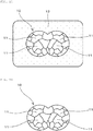
- FIGS. 1A to 1D are diagrams schematically illustrating a sintering process of copper particles.
- copper particles 10 for use in the copper particle paste mentioned above have small crystallites 11 of 30 to 100 nm in average size (average crystallite size), and have high grain boundary energy.
- the copper particles 10 have, at normal temperature, surfaces covered with an oxide film (copper oxide) 12.
- an organic compound (for example, solvent) 13 that achieves a reduction action at a firing temperature for making the copper particles sintered, present around the copper particles 10, acts as a reductant, thereby reducing the oxide film (copper oxide) 12 on the surfaces of the copper particles 10 as shown in FIG. 1B .
- the oxide film (copper oxide) 12 on the surfaces of the copper particles 10 is reduced, the copper particles 10 which have a small average crystallite diameter and high grain boundary energy undergo neck growth even at low temperatures around the reflow temperature to unite as shown in FIG. 1C , thereby increasing the crystallite diameter.
- the copper particles 10 themselves increase in size, whereas the average crystallite diameter also increase to 60 to 150 nm, and a stable copper sintered body will be thus formed.
- the copper particles constituting the copper particle paste mentioned above can be made sintered efficiently even at low temperatures by the mechanism.
- the electronic component module according to the present invention has a structure such that the external terminal included in the electronic component is electrically and mechanically connected to an object to be connected with a joint material interposed therebetween, formed by baking the copper particle paste, and the external terminal of the electronic component and the object to be connected are reliably joined with a joint part interposed therebetween, composed of a high-density copper sintered body of which voids account for a small proportion, thus making it possible to reliably provide an electronic component module with high reliability.
- the heat treatment is carried out with the electronic component and the object to be connected located such that the external terminal of the electronic component is opposed to the object to be connected, with the copper particle paste interposed therebetween, thereby causing the copper particles included in the copper particle paste to be sintered, such that the external terminal of the electronic component and the object to be connected are joined with the copper sintered body of 60 to 150 nm in average crystallite diameter.
- the external terminal of the electronic component and the object to be connected are joined with a joint part composed of the high-density copper sintered body of which voids account for a small proportion, thereby allowing a highly reliable electronic component module to be manufactured efficiently.
- the electronic component module according to First Embodiment of the present invention is an electronic component module that has a structure such that an external terminal included in an electronic component is electrically and mechanically connected to an object to be connected, with a joint material interposed therebetween, formed by making a copper particle paste sintered.
- copper particles were prepared first with the particle size peak of the particle size distribution in the range of 0.1 to 5.0 ⁇ m as copper particles, and with the average crystallite diameter before sintering in the range of 30 to 100 nm.
- liquid triethanolamine at normal temperature was prepared as an organic compound for achieving a reduction action at the firing temperature in sintering for the copper particles.
- the copper particles and the triethanolamine were combined in such a proportion of 87 : 13 in ratio by weight, and subjected to kneading to prepare a copper particle paste.
- the particle size peak of the particle size distribution for the copper particles was obtained by the following method. First, the copper particles were observed with the use of a scanning electron microscope, the horizontal feret's diameter was measured for 200 particles in the field of view. Then, the observed measurement values were converted to spheres to calculate the average volume particle diameter, and from the result, the average particle peak was obtained.
- the average crystallite diameter before sintering was obtained by the following method. First, the copper particles were subjected to an X-ray diffraction measurement, thereby finding three peaks of peaks ⁇ 111>, ⁇ 200>, and ⁇ 311>. Then, crystallite diameters were calculated by a Rietveld method with the use of the three peaks obtained, and the average value for the diameters was regarded as the average crystallite diameter.
- a first oxygen-free copper sample piece 21 of 5 mm x 5 mm in planar size and 1 mm in thickness and a second oxygen-free copper sample piece 22 of 3 mm x 3 mm in planar size and 1 mm in thickness were joined with a copper sintered body 23 obtained by firing the copper particle paste prepared in the way described above.
- the copper particle paste was applied for 40 ⁇ m in coating thickness onto the first oxygen-free copper sample piece 21 with the use of a metal mask provided with through holes that cause the copper particle paste to pass therethrough (through holes of 2000 ⁇ m in diameter and circular in planar shape).
- the second oxygen-free copper sample piece 22 was disposed on the copper particle paste applied to the first oxygen-free copper sample piece 21, and subjected to firing under the conditions of firing temperature: 230°C, firing time: 60 min, and firing atmosphere: nitrogen without particularly applying any stress, thereby, as shown in FIG. 2 , joining the first oxygen-free copper sample piece 21 and the second oxygen-free copper sample piece 22 with the joint material (the copper sintered body of the copper particle paste sintered) 23 interposed therebetween.
- the joint strength between the first oxygen-free copper sample piece 21 and the second oxygen-free copper sample piece 22 was measured.
- the joint strength was measured by measuring the shear strength with the use of a general bond tester Dage 4000 from Dage.
- the lower first oxygen-free copper sample piece 21 was fixed with a fixing jig, and shearing was applied at a shear rate of 50 ⁇ m/s and a distance of 50 ⁇ m from the surface of the oxygen-free copper sample piece 21 to a head of the tool with the use of a shearing tool 24 of 4 mm in tool width. Then, the fracture surface was photographed, and the joint area was measured by image processing.
- the shear strength value was divided by the joint area to obtain the shear strength (MPa) per unit area.
- the average crystallite diameter before firing was measured by a method of applying an ink of the copper particle paste onto a glass plate, calculating crystallite diameters by a Rietveld method from the three peaks of peaks ⁇ 111>, ⁇ 200>, and ⁇ 311> obtained by the method described above, that is, the X-ray diffraction measurement, and figuring out the average value for the diameters.
- the average crystallite diameter after firing was measured by a method of extracting the sintered body subjected to shearing with the use of tweezers, disposing the body on a glass plate, calculating crystallite diameters by a Rietveld method from the three peaks of peaks ⁇ 111>, ⁇ 200>, and ⁇ 311> obtained by the method described above, that is, the X-ray diffraction measurement, and figuring out the average value for the diameters.
- the copper particle paste was applied by printing for 40 ⁇ m in coating thickness onto the first non-oxygen copper sample piece 21 with the use of a metal mask provided with through holes of 2000 ⁇ m (2 mm) in diameter and circular in planar shape, and subjected to firing under the conditions of firing temperature: 230°C, firing time: 60 min, and firing atmosphere: nitrogen, thereby checking the crystallite diameters before and after firing.
- FIGS. 4A and 4B and 5A and 5B show micrographs (SEM images) of copper particles before and after firing copper particle pastes using the copper particles within the range specified by the requirement of the present invention and the copper particles outside the range.
- FIG. 4A is a micrograph (SEM image) showing the state of the copper particles before the firing in the copper particle paste using the copper particles of 56.7 nm in average crystallite diameter within the range specified by the requirement of the present invention
- FIG. 4B is a micrograph (SEM image) showing the state of the copper particles after the firing.
- FIG. 5A is a micrograph (SEM image) showing the state of the copper particles before the firing in the copper particle paste using the copper particles of 107.2 nm in average crystallite diameter outside the range specified by the requirement of the present invention
- FIG. 5B is a micrograph (SEM image) showing the state of the copper particles after the firing.
- the triethanolamine used in the copper particle paste described above as an organic compound (solvent) that achieves a reduction action at a firing temperature for making the copper particles sintered was checked for reducing performance by the following method.
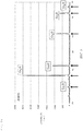
- FIG. 6A is a diagram showing an XRD chart in the case of heating the copper (I) oxide powder with the triethanolamine applied for 10 min at 230°C as a temperature condition near the melting point of Sn commonly used as an electrode material
- FIG. 6B is a diagram showing an XRD chart in the case of heating the copper (I) oxide powder with the triethanolamine applied for 10 min at 200°C.
- organic compound for achieving a reduction action it is also possible to use yet other organic compounds as the organic compound for achieving a reduction action. While it is desirable in the present invention to use a liquid organic compound at normal temperature as the organic compound for achieving a reduction action mentioned above, it is also possible to use solid substances at normal temperature in some cases, and in that regard, the substances can be dissolved in other solvents, if necessary, and used.
- FIG. 7 is a diagram illustrating an electronic component module according to an embodiment (First Embodiment) of the present invention, which has a structure electrically and mechanically connected to objects to be connected, with a joint material interposed therebetween, formed by the sintered copper particle paste prepared in the way described above.
- This electronic component module 30 is an electronic component module that has a structure such that as shown in FIG. 7 , gold bumps (external terminals) 33 formed on surface electrodes 32 of an IC chip (electronic component according to the present invention) 31 are electrically and mechanically connected onto mounting electrodes (objects to be connected) 36 of, for example, copper, formed on a circuit board 35, with a copper sintered body (joint material) 34 interposed therebetween, and such that the IC chip (electronic component) 31 is sealed with a sealing resin 37.
- gold bumps (external terminals) 33 formed on surface electrodes 32 of an IC chip (electronic component according to the present invention) 31 are electrically and mechanically connected onto mounting electrodes (objects to be connected) 36 of, for example, copper, formed on a circuit board 35, with a copper sintered body (joint material) 34 interposed therebetween, and such that the IC chip (electronic component) 31 is sealed with a sealing resin 37.
- FIG. 7 shows the structure of the IC chip 31 mounted on the circuit board 35
- other electronic components may be mounted such as a chip capacitor and a chip resistance.
- the copper sintered body 34 for the joint material mentioned above is formed by baking the copper particle paste mentioned above, and is a copper sintered body with an average crystallite diameter within the range of 60 to 150 nm after sintering.
- the circuit board 35 is first prepared which includes mounting electrodes (land electrodes) 36 on the surface thereof.
- the IC chip (the electronic component according to the present invention) 31 is prepared which has the gold bumps (external terminals) 33 formed on the surface electrodes 32.
- the copper particle paste mentioned above is applied onto the mounting electrodes 36 on the circuit board 35, and the IC chip (electronic component) 31 is mounted onto the mounting electrodes 36 on the circuit board 35 in such a manner that the gold bumps (external terminals) 33 on the IC chip (electronic component) 31 are located on the copper particle paste applied onto the mounting electrodes 36 on the circuit board 35.
- the copper particles included in the copper particle paste are subjected to sintering by firing at 230°C in a nitrogen atmosphere (inert atmosphere), thereby connecting the gold bumps (external terminals) 33 to the mounting electrode (objects to be connected) 36 with a copper sintered body (joint material) 34 interposed therebetween.
- the IC chip (electronic component) 31 mounted on the circuit board 35 is subjected to sealing with the sealing resin 37.
- the electronic component module 30 is obtained which is structured as shown in FIG. 7 .
- This electronic component module 30 has a structure such that the gold bumps (external terminals) 33 on the IC chip (electronic component) 31 are electrically and mechanically connected to the mounting electrodes (objects to be connected) 36 of the circuit board 35 to be connected, with the copper sintered body (joint material) 34 with an average crystallite diameter in the range of 60 to 150 nm after the firing, which is formed by baking the copper particle paste mentioned above.
- a highly reliable electronic component module can be provided where the gold bumps (external terminals) 33 on the IC chip (electronic component) 31 and the mounting electrodes (objects to be connected) 36 are reliably joined with the joint material 34 of the high-density copper sintered body of which voids account for a small proportion.
- the heat treatment is carried out with the IC chip (electronic component) 31 and the mounting electrodes (objects to be connected) 36 located such that the gold bumps (external terminals) 33 on the IC chip (electronic component) 31 are opposed to the objects 36 to be connected with the copper particle paste interposed therebetween to serve as the copper sintered body 34 after firing, thereby making it possible to join the gold bumps (external terminals) 33 on the IC chip (electronic component) 31 and the objects 36 to be connected with the joint material (copper sintered body) 34 of the high-density copper sintered body of which voids account for a small proportion.
- a highly reliable electronic component module can be manufactured efficiently where the gold bumps (external terminals) 33 on the IC chip (electronic component) 31 and the objects 36 to be connected are joined reliably.
- the heat treatment is carried out without applying any outside force, thus making it possible to reduce damage to the IC chip (electronic component) 31, and making it possible to form minute joint parts.
- the bumps on the IC chip are composed of gold
- the mounting electrodes (land electrodes) are composed of copper
- FIG. 8 is a diagram illustrating an electronic component module according to an embodiment (Second Embodiment) of the present invention.
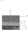
- This electronic component module 40 is an electronic component module that has a structure such that external terminals 42 of copper provided on a multilayer ceramic capacitor 41 are electrically and mechanically connected to mounting electrodes (objects to be connected in the present invention) 46 of copper formed on a circuit board (alumina board) 45, with a copper sintered body (joint material) 44 interposed therebetween, as shown in FIG. 8 .
- the joint strength is 45 MPa between the mounting electrodes (land electrodes) 46 and the external electrodes 42.
- This electronic component module 40 is formed by applying a copper particle paste to serve as the copper sintered body 44 after firing onto the mounting electrodes (land electrodes) 46 formed on the surface of the circuit board 45, disposing the multilayer ceramic capacitor 41 with the external terminals 42 formed at both ends such that the mounting electrodes (land electrodes) 46 and the external terminals 42 are opposed with the copper particle paste interposed therebetween, and carrying out firing at 230°C in a nitrogen atmosphere (inert atmosphere) without particularly applying any outside force, thereby providing the sintered copper particles included in the copper particle paste.
- FIG. 9 is a micrograph (SEM image) of a vicinity of the joint part between the multilayer ceramic capacitor 41 and the circuit board 45.
- the constituent material of the external terminals on the multilayer ceramic capacitor is not limited to copper, but may be formed from gold, silver, silver-palladium, nickel, or the like.
- the copper may contain glass.
- FIG. 10 is a diagram illustrating an electronic component with metallic terminals (a broad-sense electronic component module) according to another embodiment (Third Embodiment) of the present invention.
- the electronic component (for example, multilayer ceramic capacitor) 50 shown in FIG. 10 is the electronic component 50 with metallic terminals, which is obtained by joining metallic terminals (L-shaped metallic terminals in this example) 53 to external electrodes 52 formed on the surface of an electronic component element 51, with a copper sintered body (joint material) 54 formed by baking the copper particle paste mentioned above.
- the electronic component 50 with the metallic terminals according to Third Embodiment can be prepared easily and reliably, for example, by applying the copper particle paste to the external electrodes 52 formed on the electronic component element 51 or the metallic terminals 53, and applying a heat treatment under a predetermined condition with both the electrodes and terminals joined, thereby providing the sintered copper particles in the copper particle paste.
- the electronic component 50 with the metallic terminals has high reliability, because the external electrodes 52 on the electronic component element 51 and the metallic terminals 53 to be connected are joined reliably with the joint material (copper sintered body) 54 of the high-density copper sintered body of which voids account for a small proportion.
- the metallic terminals are not to be considered limited to the configuration as mentioned above, but may be metallic terminals constituting another part of the electronic component. Also in that case, a similar effect can be achieved.
- the constituent material of the metallic terminal 53 is not particularly limited, but it is possible to use a material composed of gold, silver, copper, silver-palladium, nickel, or the like.
- the copper particle paste mentioned above is not to be considered limited to the application such as the electronic component modules described in First and Second Embodiments and the electronic component with the metallic terminals (broad-sense electronic component module) described in Third Embodiment, but it is also possible to apply the paste to intended uses such as, for example:
Landscapes
- Engineering & Computer Science (AREA)
- Chemical & Material Sciences (AREA)
- Microelectronics & Electronic Packaging (AREA)
- Manufacturing & Machinery (AREA)
- Dispersion Chemistry (AREA)
- Spectroscopy & Molecular Physics (AREA)
- Physics & Mathematics (AREA)
- Composite Materials (AREA)
- Materials Engineering (AREA)
- Mechanical Engineering (AREA)
- Nanotechnology (AREA)
- Powder Metallurgy (AREA)
- Wire Bonding (AREA)
- Electric Connection Of Electric Components To Printed Circuits (AREA)
- Conductive Materials (AREA)
Abstract
Description
- The present invention relates to an electronic component module manufactured with the use of a copper particle paste, and a method for manufacturing an electronic component module.
- With the recent development of electronics technology, electronic component modules have been widely used which are obtained by, for example, mounting surface-mount electronic components onto circuit boards.
- Further, for mounting the surface-mount electronic components (hereinafter, simply referred to as electronic components) onto the circuit boards, external terminals of the electronic components are mechanically and electrically connected to mounting electrodes (objects to be connected) provided on circuit boards with the use of conductive joint materials.
- As such a joint material, Patent Document 1 suggests a sinterable joint material of a liquid or paste including copper nanoparticles of 1000 nm or less in particle size, where particle size peaks in the particle size distribution on the basis of the number of the copper nanoparticles include one or more peaks in each of a zone of 1 to 35 nm in particle size and a zone of more than 35 nm and 1000 nm or less in particle size, and the copper nanoparticles include primary particles and secondary particles of primary particles fused.
- Furthermore, Patent Document 1 discloses the above-mentioned sinterable joint material containing a dispersant (dispersion stabilizer), and discloses an atmosphere of hydrogen, formic acid, or ethanol as a reducing atmosphere in a firing step.
- Patent Document 1 also discloses applying a sintering heat treatment while applying pressure in the direction of joining an electronic component, in the case of joining the electronic component with the use of the sintering joint material.
- Patent Document 1:
Japanese Patent Application Laid-Open No. 2013-91835 - However, when there is a particle size peak in the zone of 1 to 35 nm in particle size, particles of such particle sizes, that is, particles of smaller sizes are likely to be agglomerated, and easily oxidized due to the large specific surface area, and there is thus the problem of poor material stability.
- In addition, in the case of containing the dispersant, a contraction in volume is likely to be caused in firing to form voids, and there is thus the problem of decreasing the joint strength.
- Furthermore, when the atmosphere of hydrogen, formic acid, or ethanol is regarded as a firing atmosphere, and for example, when the joint region is large between an electronic component and an object to be connected, there is the problem of failing to supply the reducing atmosphere gas into the inner region of the joint part, thereby making it difficult to fire the inner region in a desirable reducing atmosphere. More specifically, firing is more likely to proceed in the vicinity of the outer periphery of the joint part in contact with the reducing atmosphere, whereas firing is less likely to be proceed in the inner region, and a non-sintered region will be formed in the inner region, thereby leading to the problem of decreasing the joint strength.
- The present invention is intended to solve the problems mentioned above, and an object of the invention is to provide an electronic component module manufactured with the use of a copper particle paste which is excellent in stability (oxidation resistance) of copper particles as a conductive component, unlikely to form voids, able to form a joint part with high joint reliability, and able to ensure that not only the vicinity of the surface of the joint material constituting the joint part, but also the inner part of the joint material are made sintered, and a method for manufacturing the electronic component module.
- In order to solve the problems mentioned above, an electronic component module according to the present invention is an electronic component module including a structure such that an external terminal included in an electronic component is electrically and mechanically connected to an object to be connected, with a joint material interposed therebetween, characterized in that the joint material is formed by making a copper particle paste sintered, the copper particle paste containing: copper particles having a particle size peak in the range of 0.1µm to 5.0 µm in the particle size distribution and an average crystallite diameter before sintering in the range of 30 nm to 100 nm, and including, on particle surfaces, no dispersant that suppresses agglomeration; and an organic compound that achieves a reduction action at a firing temperature for making the copper particles sintered.
- In addition, the joint material is preferably a copper sintered body with an average crystallite diameter in the range of 60 nm to 150 nm for the sintered copper particles.
- The adjustment of the average crystallite diameter from 60 nm to 150 nm after being sintered forms a stable sintered body.
- In addition, in the copper particle paste mentioned above, the organic compound is preferably an organic compound having a hydroxy group.
- The use of the organic compound having a hydroxy group as the organic compound that achieves a reduction action at the firing temperature for making the copper particles sintered makes it possible to remove an oxide film formed on the surfaces of the copper particles in a firing step, and ensure that copper is sintered without oxidizing the copper in the firing step, thereby allowing the present invention to be made more effective.
- In addition, the organic compound preferably includes at least one selected from the group consisting of triethanolamine, glycerin, ethylene glycol, triethylene glycol, diethylene glycol, and dipropylene glycol.
- The use of at least one from the group mentioned above can make the present invention more effective.
- In addition, the object to be connected is preferably a mounting electrode provided on a circuit board.
- Connecting the external terminal of the electronic component to the mounting electrode provided on the circuit board by the method according to the present invention makes it possible to reliably manufacture a highly reliable electronic component module which has a structure such that a surface-mount electronic component such as an IC chip and a multilayer ceramic capacitor, for example, is mounted on the circuit board.
- In addition, the object to be connected is preferably a metallic terminal attached to the external terminal.
- Attaching the external terminal of the electronic component to the metallic terminal by the method according to the present invention makes it possible to reliably manufacture a highly reliable electronic component module with a terminal.
- Furthermore, a method for manufacturing an electronic component module according to the present invention is a method for manufacturing an electronic component module including a structure such that an external terminal included in an electronic component is electrically and mechanically connected to an object to be connected, with a joint material interposed therebetween, the method characterized in that it includes the steps of: locating the electronic component and the object to be joined such that the external terminal of the electronic component is opposed to the object to be connected, with a copper particle paste interposed therebetween, the copper particle paste containing copper particles having a particle size peak in the range of 0.1 µm to 5.0 µm in the particle size distribution and an average crystallite diameter before sintering in the range of 30 nm to 100 nm, and including, on particle surfaces, no dispersant that suppresses agglomeration, and an organic compound that achieves a reduction action at a firing temperature for making the copper particles sintered; and carrying out a heat treatment to cause the copper particles included in the copper particle paste to be sintered, thereby forming a copper sintered body of 60 to 150 nm in average crystallite diameter for the copper particles, and thus joining the external terminal of the electronic component and the object to be connected, with the copper sintered body interposed therebetween.
- In the method for manufacturing an electronic component module according to the present invention, the heat treatment is preferably carried out without applying an outside force, with the electronic component disposed on the object to be joined, such that the external terminal of the electronic component is opposed to the object to be connected, with the copper particle paste interposed therebetween.
- The use of the copper particle paste as described above makes it possible to carry out the heat treatment without applying any outside force, and applying no pressure makes it possible to reduce damage to the electronic component, and allows a minute joint part to be formed.
- In addition, the heat treatment is preferably carried out in an inert atmosphere.
- The heat treatment in the inert atmosphere makes it possible to further ensure that the copper particles constituting the copper particle paste are made sintered, thereby allowing the present invention to be made more effective.
- The copper particles with a particle size peak in the range of 0.1 to 5.0 µm in the particle size distribution, which are used as copper particles constituting the copper particle paste mentioned above, are not excessively fine, and thus copper particles which are unlikely to be oxidized and excellent in stability, on the other hand, small from 30 to 100 nm in average crystallite diameter in terms of sinterability, able to be sintered at low temperatures of 300°C or lower, and after being sintered, become a copper sintered body around 60 to 150 nm in average crystallite diameter, thereby serving as a stable joint material.
- In addition, the copper particles have, at the surfaces thereof, no dispersant for suppressing agglomeration, and a sintered body can be thus obtained which has a high-density copper sintered body obtained by sintering, and has a low proportion of voids.
- More specifically, while so-called nanoparticles of 100 nm or less in copper particle size are agglomerated in the absence of a dispersant, the particle size peak of the particle size distribution for the copper particles falls within the range of 0.1 to 5.0 µm in the copper particle paste mentioned above, thus making it possible to suppress agglomeration without using any dispersant.
- It is to be noted that in the case of nanoparticles of 100 nm or less in average crystallite diameter, it is possible to make the nanoparticles sintered at low temperatures due to the effect of the nanoparticles (nanosized effect), but the present invention allows low-temperature sintering at low temperatures of 300°C or lower with the average crystallite diameter for the copper particles in the range of 30 to 100 nm.
- More specifically, increasing the particle size peak of the particle size distribution for the copper particles to 0.1 to 5.0 µm and reducing the average crystallite diameter to 30 to 100 nm make it possible to prevent agglomeration without combining any dispersant, and allow low-temperature sintering at 300°C or lower.
- In addition, the cooper particle paste mentioned above contains the organic compound (for example, solvent) that achieves a reduction action at the firing temperature for making the copper particles sintered, and the reduction action of the organic compound thus reduces a copper oxide on the copper particle surfaces, which causes sintering to be constrained, thereby making it possible to achieve sintering under an inert atmosphere particularly without the need for firing in a reducing atmosphere. It is to be noted that while firing under a reducing atmosphere with the use of a reducing gas is performed, when the copper particle paste is used as a joint material, there is a problem that sintering proceeds at the surface and peripheral part of the joint part, whereas sintering is likely to be insufficient within the joint part, containing the organic compound (for example, solvent) that achieves a reduction action as described above can solve this problem without the need for firing under a reducing atmosphere.
- It is to be noted that it is believed to be by the mechanism described below that the copper particles in the copper particle paste are sintered at low temperatures.
-
FIGS. 1A to 1D are diagrams schematically illustrating a sintering process of copper particles. - As shown in
FIG. 1A ,copper particles 10 for use in the copper particle paste mentioned above havesmall crystallites 11 of 30 to 100 nm in average size (average crystallite size), and have high grain boundary energy. In addition, thecopper particles 10 have, at normal temperature, surfaces covered with an oxide film (copper oxide) 12. - When the copper particle paste (copper particles) 1 is heated to a reflow temperature (for example, 230°C), an organic compound (for example, solvent) 13 that achieves a reduction action at a firing temperature for making the copper particles sintered, present around the
copper particles 10, acts as a reductant, thereby reducing the oxide film (copper oxide) 12 on the surfaces of thecopper particles 10 as shown inFIG. 1B . - Thus, when the oxide film (copper oxide) 12 on the surfaces of the
copper particles 10 is reduced, thecopper particles 10 which have a small average crystallite diameter and high grain boundary energy undergo neck growth even at low temperatures around the reflow temperature to unite as shown inFIG. 1C , thereby increasing the crystallite diameter. As a result, as shown inFIG. 1D , thecopper particles 10 themselves increase in size, whereas the average crystallite diameter also increase to 60 to 150 nm, and a stable copper sintered body will be thus formed. - The copper particles constituting the copper particle paste mentioned above can be made sintered efficiently even at low temperatures by the mechanism.
- In addition, the electronic component module according to the present invention has a structure such that the external terminal included in the electronic component is electrically and mechanically connected to an object to be connected with a joint material interposed therebetween, formed by baking the copper particle paste, and the external terminal of the electronic component and the object to be connected are reliably joined with a joint part interposed therebetween, composed of a high-density copper sintered body of which voids account for a small proportion, thus making it possible to reliably provide an electronic component module with high reliability.
- Furthermore, in the method for manufacturing an electronic component module according to the present invention, the heat treatment is carried out with the electronic component and the object to be connected located such that the external terminal of the electronic component is opposed to the object to be connected, with the copper particle paste interposed therebetween, thereby causing the copper particles included in the copper particle paste to be sintered, such that the external terminal of the electronic component and the object to be connected are joined with the copper sintered body of 60 to 150 nm in average crystallite diameter. Thus, it becomes possible to ensure that the external terminal of the electronic component and the object to be connected are joined with a joint part composed of the high-density copper sintered body of which voids account for a small proportion, thereby allowing a highly reliable electronic component module to be manufactured efficiently.
-
-
FIG. 1A is a diagram schematically illustrating a step of a sintering process for copper particles for use in a copper particle paste. -
FIG. 1B is a diagram schematically illustrating another step of the sintering process for copper particles for use in the copper particle paste. -
FIG. 1C is a diagram schematically illustrating yet another step of the sintering process for copper particles for use in the copper particle paste. -
FIG. 1D is a diagram schematically illustrating yet another step of the sintering process for copper particles for use in the copper particle paste. -
FIG. 2 is a diagram illustrating a joint part joined with the use of the copper particle paste. -
FIG. 3 is a diagram for explaining a method for measuring the joint strength of joint part joined with the use of the copper particle paste. -
FIG. 4A is a micrograph (SEM image) showing the state of copper particles before firing in a copper particle paste using the copper particles of 56.7 nm in average crystallite diameter. -
FIG. 4B is a micrograph (SEM image) showing the state of the copper particles after firing in the copper particle paste using the copper particles of 56.7 nm in average crystallite diameter. -
FIG. 5A is a micrograph (SEM image) showing the state of copper particles before firing in a copper particle paste using the copper particles of 107.2 nm in average crystallite diameter. -
FIG. 5B is a micrograph (SEM image) showing the state of the copper particles after firing in the copper particle paste using the copper particles of 107.2 nm in average crystallite diameter. -
FIG. 6A is a diagram for confirming an action of triethanolamine as a reductant, which illustrates an XRD chart in the case of heating a copper (I) oxide powder with the triethanolamine applied for 10 min at 230°C. -
FIG. 6B is a diagram for confirming an action of triethanolamine as a reductant, which illustrates an XRD chart in the case of heating a copper (I) oxide powder with the triethanolamine applied for 10 min at 200°C. -
FIG. 7 is a diagram illustrating the configuration of an electronic component module according to First Embodiment of the present invention. -
FIG. 8 is a diagram illustrating the configuration of an electronic component module according to Second Embodiment of the present invention. -
FIG. 9 is a micrograph (SEM image) of a vicinity of the joint part between an electronic component and a circuit board in the electronic component module according to Second Embodiment of the present invention. -
FIG. 10 is a diagram illustrating the configuration of an electronic component module according to Third Embodiment of the present invention. - Features of the present invention will be described in more detail below with reference to embodiments of the present invention.
- The electronic component module according to First Embodiment of the present invention is an electronic component module that has a structure such that an external terminal included in an electronic component is electrically and mechanically connected to an object to be connected, with a joint material interposed therebetween, formed by making a copper particle paste sintered.
- For preparing the copper particle paste to serve as the junction material, copper particles were prepared first with the particle size peak of the particle size distribution in the range of 0.1 to 5.0 µm as copper particles, and with the average crystallite diameter before sintering in the range of 30 to 100 nm.
- In addition, liquid triethanolamine at normal temperature was prepared as an organic compound for achieving a reduction action at the firing temperature in sintering for the copper particles.
- Then, the copper particles and the triethanolamine were combined in such a proportion of 87 : 13 in ratio by weight, and subjected to kneading to prepare a copper particle paste.
- It is to be noted that the particle size peak of the particle size distribution for the copper particles was obtained by the following method. First, the copper particles were observed with the use of a scanning electron microscope, the horizontal feret's diameter was measured for 200 particles in the field of view. Then, the observed measurement values were converted to spheres to calculate the average volume particle diameter, and from the result, the average particle peak was obtained.
- In addition, the average crystallite diameter before sintering was obtained by the following method. First, the copper particles were subjected to an X-ray diffraction measurement, thereby finding three peaks of peaks <111>, <200>, and <311>. Then, crystallite diameters were calculated by a Rietveld method with the use of the three peaks obtained, and the average value for the diameters was regarded as the average crystallite diameter.
- With the use of the copper particle paste prepared in the way described above, oxygen-free copper sample pieces were joined to each other and checked for joint strength by the method described below.
- In this regard, as shown in
FIG. 2 , a first oxygen-freecopper sample piece 21 of 5 mm x 5 mm in planar size and 1 mm in thickness and a second oxygen-freecopper sample piece 22 of 3 mm x 3 mm in planar size and 1 mm in thickness were joined with acopper sintered body 23 obtained by firing the copper particle paste prepared in the way described above. - For joining the first oxygen-free
copper sample piece 21 and the second oxygen-freecopper sample piece 22 with the use of the copper particle paste, the copper particle paste was applied for 40 µm in coating thickness onto the first oxygen-freecopper sample piece 21 with the use of a metal mask provided with through holes that cause the copper particle paste to pass therethrough (through holes of 2000 µm in diameter and circular in planar shape). - Then, the second oxygen-free
copper sample piece 22 was disposed on the copper particle paste applied to the first oxygen-freecopper sample piece 21, and subjected to firing under the conditions of firing temperature: 230°C, firing time: 60 min, and firing atmosphere: nitrogen without particularly applying any stress, thereby, as shown inFIG. 2 , joining the first oxygen-freecopper sample piece 21 and the second oxygen-freecopper sample piece 22 with the joint material (the copper sintered body of the copper particle paste sintered) 23 interposed therebetween. - Then, the joint strength between the first oxygen-free
copper sample piece 21 and the second oxygen-freecopper sample piece 22 was measured. The joint strength was measured by measuring the shear strength with the use of a general bond tester Dage 4000 from Dage. - It is to be noted that for the measurement, as shown in
FIG. 3 , the lower first oxygen-freecopper sample piece 21 was fixed with a fixing jig, and shearing was applied at a shear rate of 50 µm/s and a distance of 50 µm from the surface of the oxygen-freecopper sample piece 21 to a head of the tool with the use of ashearing tool 24 of 4 mm in tool width. Then, the fracture surface was photographed, and the joint area was measured by image processing. - Then, the shear strength value was divided by the joint area to obtain the shear strength (MPa) per unit area.
- As a result, it has been confirmed that a high strength of 36 MPa is achieved as the shear strength.
- The average crystallite diameter before firing was measured by a method of applying an ink of the copper particle paste onto a glass plate, calculating crystallite diameters by a Rietveld method from the three peaks of peaks <111>, <200>, and <311> obtained by the method described above, that is, the X-ray diffraction measurement, and figuring out the average value for the diameters. The average crystallite diameter after firing was measured by a method of extracting the sintered body subjected to shearing with the use of tweezers, disposing the body on a glass plate, calculating crystallite diameters by a Rietveld method from the three peaks of peaks <111>, <200>, and <311> obtained by the method described above, that is, the X-ray diffraction measurement, and figuring out the average value for the diameters.
- More specifically, the copper particle paste was applied by printing for 40 µm in coating thickness onto the first non-oxygen
copper sample piece 21 with the use of a metal mask provided with through holes of 2000 µm (2 mm) in diameter and circular in planar shape, and subjected to firing under the conditions of firing temperature: 230°C, firing time: 60 min, and firing atmosphere: nitrogen, thereby checking the crystallite diameters before and after firing. - As a result, it has been confirmed that the average crystallite diameter of 62 nm at the stage before the firing is increased up to 102 µm after the firing.
- As just described, when the average crystallite diameter at the stage before the firing is reduced so as to meet the range specified by the requirement of the present invention, it becomes possible to prevent agglomeration of the copper particles without using any dispersant, and the mechanism described previously with reference to
FIGS. 1A to 1D makes it possible to achieve sintering at lower temperatures. As a result, it becomes possible to form a joint material of a high-density copper sintered body of which voids account for a small proportion, without requiring any firing at high temperatures. -
FIGS. 4A and 4B and5A and 5B show micrographs (SEM images) of copper particles before and after firing copper particle pastes using the copper particles within the range specified by the requirement of the present invention and the copper particles outside the range. - It is to be noted that
FIG. 4A is a micrograph (SEM image) showing the state of the copper particles before the firing in the copper particle paste using the copper particles of 56.7 nm in average crystallite diameter within the range specified by the requirement of the present invention, whereasFIG. 4B is a micrograph (SEM image) showing the state of the copper particles after the firing. - In addition,
FIG. 5A is a micrograph (SEM image) showing the state of the copper particles before the firing in the copper particle paste using the copper particles of 107.2 nm in average crystallite diameter outside the range specified by the requirement of the present invention, whereasFIG. 5B is a micrograph (SEM image) showing the state of the copper particles after the firing. - As can be seen from
FIGS. 5A and 5B , in the case of the copper particle paste using thecopper particles 10 of 107.2 nm in average crystallite diameter outside the range specified by the requirement of the present invention, thecopper particles 10 have been hardly found to undergo neck growth. - In contrast, as can be seen from
FIGS. 4A and 4B , in the case of the copper particle paste using thecopper particles 10 of 56.7 nm in average crystallite diameter within the range specified by the requirement of the present invention, it has been confirmed that thecopper particles 10 undergo neck growth, that is, are sintered sufficiently. - The triethanolamine used in the copper particle paste described above as an organic compound (solvent) that achieves a reduction action at a firing temperature for making the copper particles sintered was checked for reducing performance by the following method.
- For confirming the reducing performance of the triethanolamine, an experiment was carried out as described below with the use of a commercially available copper (I) oxide (Cu2O) powder. First, a copper (I) oxide powder was disposed on a glass substrate, liquid triethanolamine at normal temperature was applied thereto, and after heating for 10 min at a predetermined temperature on a hot plate, a composition analysis was carried out by XRD.
- The results in the case of heating for 10 min at 200°C, and in the case of heating for 10 min at 230°C as a temperature condition near the melting point of Sn commonly used as an electrode material will be described herein with respect to
FIGS. 6A and6B . - It is to be noted that
FIG. 6A is a diagram showing an XRD chart in the case of heating the copper (I) oxide powder with the triethanolamine applied for 10 min at 230°C as a temperature condition near the melting point of Sn commonly used as an electrode material, whereasFIG. 6B is a diagram showing an XRD chart in the case of heating the copper (I) oxide powder with the triethanolamine applied for 10 min at 200°C. - As a result, as shown in
FIG. 6B , it has been confirmed that in the case of the heating temperature of 200°C, there is no Cu peak found while the peak of copper (I) oxide (Cu2O) remains high, thus failing to achieve any reduction action. - On the other hand, it has been confirmed that in the case of the temperature of 230°C as a temperature condition near the melting point of Sn commonly used as an electrode material, as shown in
FIG. 6A , there is a clear Cu peak found while the peak of copper (I) oxide (Cu2O) is reduced, that is, a reduction action is achieved. - It is to be noted that while the triethanolamine was used as an organic compound that has reducing performance in this embodiment, it has been confirmed that organic compounds having a hydroxy group have reducing performance, such as glycerin, ethylene glycol, triethylene glycol, diethylene glycol, and dipropylene glycol, besides triethanolamine, and it is also possible to use these substances as an organic compound that has reducing performance.
- Further, it is also possible to use yet other organic compounds as the organic compound for achieving a reduction action. While it is desirable in the present invention to use a liquid organic compound at normal temperature as the organic compound for achieving a reduction action mentioned above, it is also possible to use solid substances at normal temperature in some cases, and in that regard, the substances can be dissolved in other solvents, if necessary, and used.
-
FIG. 7 is a diagram illustrating an electronic component module according to an embodiment (First Embodiment) of the present invention, which has a structure electrically and mechanically connected to objects to be connected, with a joint material interposed therebetween, formed by the sintered copper particle paste prepared in the way described above. - This
electronic component module 30 is an electronic component module that has a structure such that as shown inFIG. 7 , gold bumps (external terminals) 33 formed onsurface electrodes 32 of an IC chip (electronic component according to the present invention) 31 are electrically and mechanically connected onto mounting electrodes (objects to be connected) 36 of, for example, copper, formed on acircuit board 35, with a copper sintered body (joint material) 34 interposed therebetween, and such that the IC chip (electronic component) 31 is sealed with a sealingresin 37. - It is to be noted that while
FIG. 7 shows the structure of theIC chip 31 mounted on thecircuit board 35, other electronic components may be mounted such as a chip capacitor and a chip resistance. - The copper sintered
body 34 for the joint material mentioned above is formed by baking the copper particle paste mentioned above, and is a copper sintered body with an average crystallite diameter within the range of 60 to 150 nm after sintering. - Next, a method for manufacturing the
electronic component module 30 will be described. For manufacturing the electronic component module, thecircuit board 35 is first prepared which includes mounting electrodes (land electrodes) 36 on the surface thereof. - In addition, the IC chip (the electronic component according to the present invention) 31 is prepared which has the gold bumps (external terminals) 33 formed on the
surface electrodes 32. - Then, the copper particle paste mentioned above is applied onto the mounting
electrodes 36 on thecircuit board 35, and the IC chip (electronic component) 31 is mounted onto the mountingelectrodes 36 on thecircuit board 35 in such a manner that the gold bumps (external terminals) 33 on the IC chip (electronic component) 31 are located on the copper particle paste applied onto the mountingelectrodes 36 on thecircuit board 35. Then, without particularly pressing the IC chip (electronic component) 31 toward thecircuit board 35, the copper particles included in the copper particle paste are subjected to sintering by firing at 230°C in a nitrogen atmosphere (inert atmosphere), thereby connecting the gold bumps (external terminals) 33 to the mounting electrode (objects to be connected) 36 with a copper sintered body (joint material) 34 interposed therebetween. - Then, the IC chip (electronic component) 31 mounted on the
circuit board 35 is subjected to sealing with the sealingresin 37. Thus, theelectronic component module 30 is obtained which is structured as shown inFIG. 7 . - This
electronic component module 30 has a structure such that the gold bumps (external terminals) 33 on the IC chip (electronic component) 31 are electrically and mechanically connected to the mounting electrodes (objects to be connected) 36 of thecircuit board 35 to be connected, with the copper sintered body (joint material) 34 with an average crystallite diameter in the range of 60 to 150 nm after the firing, which is formed by baking the copper particle paste mentioned above. - Accordingly, a highly reliable electronic component module can be provided where the gold bumps (external terminals) 33 on the IC chip (electronic component) 31 and the mounting electrodes (objects to be connected) 36 are reliably joined with the
joint material 34 of the high-density copper sintered body of which voids account for a small proportion. - In addition, according to the method for manufacturing the electronic component module as described above, the heat treatment is carried out with the IC chip (electronic component) 31 and the mounting electrodes (objects to be connected) 36 located such that the gold bumps (external terminals) 33 on the IC chip (electronic component) 31 are opposed to the
objects 36 to be connected with the copper particle paste interposed therebetween to serve as the copper sinteredbody 34 after firing, thereby making it possible to join the gold bumps (external terminals) 33 on the IC chip (electronic component) 31 and theobjects 36 to be connected with the joint material (copper sintered body) 34 of the high-density copper sintered body of which voids account for a small proportion. - Accordingly, a highly reliable electronic component module can be manufactured efficiently where the gold bumps (external terminals) 33 on the IC chip (electronic component) 31 and the
objects 36 to be connected are joined reliably. - In addition, the heat treatment is carried out without applying any outside force, thus making it possible to reduce damage to the IC chip (electronic component) 31, and making it possible to form minute joint parts.
- It is to be noted that while a case where the bumps on the IC chip (electronic component) are composed of gold, whereas the mounting electrodes (land electrodes) are composed of copper has been explained as an example in First Embodiment, it is possible to use Ag, Cu, Ni, Ag-Pd, and the like as a constituent material for the bumps, and it is possible to use Au, Ag, Ni, Ag-Pd, and the like as a constituent material for the mounting electrodes (land electrodes).
-
FIG. 8 is a diagram illustrating an electronic component module according to an embodiment (Second Embodiment) of the present invention. - This
electronic component module 40 is an electronic component module that has a structure such thatexternal terminals 42 of copper provided on a multilayerceramic capacitor 41 are electrically and mechanically connected to mounting electrodes (objects to be connected in the present invention) 46 of copper formed on a circuit board (alumina board) 45, with a copper sintered body (joint material) 44 interposed therebetween, as shown inFIG. 8 . - In this
electronic component module 40, it has been confirmed that the joint strength is 45 MPa between the mounting electrodes (land electrodes) 46 and theexternal electrodes 42. - This
electronic component module 40 is formed by applying a copper particle paste to serve as the copper sinteredbody 44 after firing onto the mounting electrodes (land electrodes) 46 formed on the surface of thecircuit board 45, disposing the multilayerceramic capacitor 41 with theexternal terminals 42 formed at both ends such that the mounting electrodes (land electrodes) 46 and theexternal terminals 42 are opposed with the copper particle paste interposed therebetween, and carrying out firing at 230°C in a nitrogen atmosphere (inert atmosphere) without particularly applying any outside force, thereby providing the sintered copper particles included in the copper particle paste. -
FIG. 9 is a micrograph (SEM image) of a vicinity of the joint part between the multilayerceramic capacitor 41 and thecircuit board 45. - From
FIG. 9 , it is found that theexternal terminals 42 of copper on the multilayerceramic capacitor 41 are joined to the mountingelectrodes 46 of copper on thecircuit board 45 with the joint material of the copper sinteredbody 44 interposed therebetween. - From Second Embodiment herein, it is found that without forming any Sn plated layer, solder plated layer, or the like on the
external terminals 42 on the multilayerceramic capacitor 41, theexternal terminals 42 of Cu on the multilayerceramic capacitor 41 and the mountingelectrodes 46 of copper on thecircuit board 45 are joined directly with the use of the copper particle paste mentioned above, thereby making it possible to achieve highly reliable joints without forming any intermetallic compound. - It is to be noted that the constituent material of the external terminals on the multilayer ceramic capacitor is not limited to copper, but may be formed from gold, silver, silver-palladium, nickel, or the like. In addition, the copper may contain glass.
-
FIG. 10 is a diagram illustrating an electronic component with metallic terminals (a broad-sense electronic component module) according to another embodiment (Third Embodiment) of the present invention. - The electronic component (for example, multilayer ceramic capacitor) 50 shown in
FIG. 10 is theelectronic component 50 with metallic terminals, which is obtained by joining metallic terminals (L-shaped metallic terminals in this example) 53 toexternal electrodes 52 formed on the surface of anelectronic component element 51, with a copper sintered body (joint material) 54 formed by baking the copper particle paste mentioned above. - The
electronic component 50 with the metallic terminals according to Third Embodiment can be prepared easily and reliably, for example, by applying the copper particle paste to theexternal electrodes 52 formed on theelectronic component element 51 or themetallic terminals 53, and applying a heat treatment under a predetermined condition with both the electrodes and terminals joined, thereby providing the sintered copper particles in the copper particle paste. - It is to be noted that the
electronic component 50 with the metallic terminals has high reliability, because theexternal electrodes 52 on theelectronic component element 51 and themetallic terminals 53 to be connected are joined reliably with the joint material (copper sintered body) 54 of the high-density copper sintered body of which voids account for a small proportion. - It is to be noted that the metallic terminals are not to be considered limited to the configuration as mentioned above, but may be metallic terminals constituting another part of the electronic component. Also in that case, a similar effect can be achieved. The constituent material of the
metallic terminal 53 is not particularly limited, but it is possible to use a material composed of gold, silver, copper, silver-palladium, nickel, or the like. - In addition, the copper particle paste mentioned above is not to be considered limited to the application such as the electronic component modules described in First and Second Embodiments and the electronic component with the metallic terminals (broad-sense electronic component module) described in Third Embodiment, but it is also possible to apply the paste to intended uses such as, for example:
- (a) a connection material for an integrated component provided within a multilayer ceramic substrate;
- (b) a via hole conductor forming material for interlayer connection;
- (c) an electrode forming material for forming wirings and electrodes;
- (d) a conductive sealing material; and
- (e) a connection material for die bonding.
- The present invention is not to be considered limited to the embodiments described above in yet other respects, but various applications and modifications can be made within the scope of the invention.
-
- 10: copper particle
- 11: crystallite
- 12: oxide film (copper oxide)
- 13: organic compound for achieving a reduction action (solvent)
- 21: first oxygen-free copper sample piece
- 22: second oxygen-free copper sample piece
- 23: copper sintered body obtained by firing a copper particle paste
- 24: shearing tool
- 30: electronic component module
- 31: IC chip (electronic component)
- 32: surface electrode
- 33: gold bump (external terminal)
- 34: copper sintered body (joint material)
- 35: circuit board
- 36: mounting electrode (object to be connected)
- 37: sealing resin
- 40: electronic component module
- 41: multilayer ceramic capacitor
- 42: external terminal
- 44: copper sintered body (joint material)
- 45: circuit board (alumina board)
- 46: mounting electrode (object to be connected)
- 50: electronic component
- 51: electronic component element
- 52: external electrode
- 53: metallic terminal
- 54: copper sintered body (joint material)
Claims (9)
- An electronic component module comprising a structure such that an external terminal included in an electronic component is electrically and mechanically connected to an object to be connected, with a joint material interposed therebetween,
wherein the joint material is formed by making a copper particle paste sintered, the copper particle paste containing:copper particles having a particle size peak in a range of 0.1 µm to 5.0 µm in a particle size distribution and an average crystallite diameter before sintering in a range of 30 nm to 100 nm, and comprising, on particle surfaces, no dispersant that suppresses agglomeration; andan organic compound that achieves a reduction action at a firing temperature for making the copper particles sintered. - The electronic component module according to claim 1,
wherein the joint material is a copper sintered body with an average crystallite diameter in a range of 60 nm to 150 nm for the sintered copper particles. - The electronic component module according to one of claims 1 and 2, wherein the organic compound is an organic compound having a hydroxy group.
- The electronic component module according to any of claims 1 to 3, wherein the organic compound comprises at least one selected from the group consisting of triethanolamine, glycerin, ethylene glycol, triethylene glycol, diethylene glycol, and dipropylene glycol.
- The electronic component module according to any of claims 1 to 4, wherein the object to be connected is a mounting electrode provided on the circuit board.
- The electronic component module according to any of claims 1 to 4, wherein the object to be connected is a metallic terminal attached to the external terminal.
- A method for manufacturing an electronic component module comprising a structure such that an external terminal included in an electronic component is electrically and mechanically connected to an object to be connected, with a joint material interposed therebetween,
the method comprising the steps of:locating the electronic component and the object to be joined such that the external terminal of the electronic component is opposed to the object to be connected, with a copper particle paste interposed therebetween, the copper particle paste containing copper particles having a particle size peak in a range of 0.1 µm to 5.0 µm in a particle size distribution and an average crystallite diameter before sintering in a range of 30 nm to 100 nm, and comprising, on particle surfaces, no dispersant that suppresses agglomeration, and an organic compound that achieves a reduction action at a firing temperature for making the copper particles sintered; andcarrying out a heat treatment to cause the copper particles included in the copper particle paste to be sintered, thereby forming a copper sintered body of 60 nm to 150 nm in average crystallite diameter for the copper particles, and thus joining the external terminal of the electronic component and the object to be connected, with the copper sintered body interposed therebetween. - The method for manufacturing an electronic component module according to claim 7, wherein the heat treatment is carried out without applying an outside force, with the electronic component disposed on the object to be joined, such that the external terminal of the electronic component is opposed to the object to be connected, with the copper particle paste interposed therebetween.
- The method for manufacturing an electronic component module according to one of claims 7 and 8, wherein the heat treatment is carried out in an inert atmosphere. mentioned above.
Applications Claiming Priority (2)
| Application Number | Priority Date | Filing Date | Title |
|---|---|---|---|
| JP2014019212 | 2014-02-04 | ||
| PCT/JP2015/052018 WO2015118982A1 (en) | 2014-02-04 | 2015-01-26 | Electronic component module, and manufacturing method of electronic component module |
Publications (3)
| Publication Number | Publication Date |
|---|---|
| EP3104400A1 true EP3104400A1 (en) | 2016-12-14 |
| EP3104400A4 EP3104400A4 (en) | 2017-11-15 |
| EP3104400B1 EP3104400B1 (en) | 2022-08-31 |
Family
ID=53777789
Family Applications (1)
| Application Number | Title | Priority Date | Filing Date |
|---|---|---|---|
| EP15746474.4A Active EP3104400B1 (en) | 2014-02-04 | 2015-01-26 | Manufacturing method of electronic component module |
Country Status (5)
| Country | Link |
|---|---|
| US (1) | US9860989B2 (en) |
| EP (1) | EP3104400B1 (en) |
| JP (1) | JP6337909B2 (en) |
| CN (1) | CN106170851B (en) |
| WO (1) | WO2015118982A1 (en) |
Families Citing this family (21)
| Publication number | Priority date | Publication date | Assignee | Title |
|---|---|---|---|---|
| CN107848075B (en) | 2015-09-15 | 2021-03-19 | 株式会社村田制作所 | Joining member, manufacturing method of joining member, and joining method |
| JP6528852B2 (en) | 2015-09-28 | 2019-06-12 | 株式会社村田製作所 | Heat pipe, heat dissipation part, heat pipe manufacturing method |
| EP3758048B1 (en) | 2015-10-02 | 2022-11-09 | Mitsui Mining & Smelting Co., Ltd. | A bonding junction structure |
| CN107835724B (en) * | 2015-11-05 | 2020-09-08 | 株式会社村田制作所 | Member for bonding and method for manufacturing the member for bonding |
| JP6565710B2 (en) * | 2016-01-27 | 2019-08-28 | 三菱マテリアル株式会社 | Manufacturing method of copper member assembly |
| JP2017152638A (en) * | 2016-02-26 | 2017-08-31 | 株式会社村田製作所 | Junction structure, electronic component having the junction structure, and method of forming the junction structure |
| WO2018074188A1 (en) * | 2016-10-19 | 2018-04-26 | 株式会社村田製作所 | Inductor component, method for manufacturing inductor component |
| WO2018216597A1 (en) | 2017-05-26 | 2018-11-29 | 株式会社村田製作所 | Multilayer wiring board, electronic device and method for producing multilayer wiring board |
| CN112771628B (en) * | 2018-09-28 | 2022-09-13 | 纳美仕有限公司 | Conductive paste |
| JP7170968B2 (en) * | 2019-02-22 | 2022-11-15 | 株式会社大阪ソーダ | Joining method using conductive adhesive |
| WO2020202971A1 (en) * | 2019-03-29 | 2020-10-08 | 三井金属鉱業株式会社 | Bonding material and bonded structure |
| CN110202137B (en) * | 2019-05-29 | 2021-07-20 | 深圳第三代半导体研究院 | A kind of low temperature sintered copper paste and its sintering process |
| US20240081336A1 (en) * | 2019-09-16 | 2024-03-14 | Corning Incorporated | Color stabilization of biocidal coatings |
| KR102842071B1 (en) * | 2019-09-18 | 2025-08-04 | 삼성전기주식회사 | Electronic component and board having the same mounted thereon |
| JP7380256B2 (en) * | 2020-01-28 | 2023-11-15 | 三菱マテリアル株式会社 | Joining sheet |
| WO2022163574A1 (en) * | 2021-01-28 | 2022-08-04 | 京セラ株式会社 | Wiring board |
| KR20240168931A (en) * | 2022-03-30 | 2024-12-02 | 미쓰이금속광업주식회사 | Method for manufacturing a conjugate |
| EP4503869A1 (en) * | 2022-03-30 | 2025-02-05 | Kyocera Corporation | Wiring board |
| JPWO2023189513A1 (en) * | 2022-03-30 | 2023-10-05 | ||
| WO2023210449A1 (en) * | 2022-04-28 | 2023-11-02 | 三井金属鉱業株式会社 | Copper paste for joining, method for joining body to be joined, method for producing joined body, and method for producing copper paste for joining |
| KR20260016527A (en) * | 2023-05-30 | 2026-02-03 | 주식회사 다이셀 | Polymer and photosensitive resin composition containing the same, copper paste, liquid composition, method for manufacturing semiconductor device, and method for manufacturing copper filler for semiconductor connection |
Family Cites Families (23)
| Publication number | Priority date | Publication date | Assignee | Title |
|---|---|---|---|---|
| US4859364A (en) * | 1988-05-25 | 1989-08-22 | E. I. Du Pont De Nemours And Company | Conductive paste composition |
| US5180523A (en) * | 1989-11-14 | 1993-01-19 | Poly-Flex Circuits, Inc. | Electrically conductive cement containing agglomerate, flake and powder metal fillers |
| US5652042A (en) * | 1993-10-29 | 1997-07-29 | Matsushita Electric Industrial Co., Ltd. | Conductive paste compound for via hole filling, printed circuit board which uses the conductive paste |
| JPH09198920A (en) * | 1996-01-22 | 1997-07-31 | Mitsuboshi Belting Ltd | Copper conductor paste and circuit board printed with copper conductor paste |
| US6679937B1 (en) * | 1997-02-24 | 2004-01-20 | Cabot Corporation | Copper powders methods for producing powders and devices fabricated from same |
| US6139777A (en) * | 1998-05-08 | 2000-10-31 | Matsushita Electric Industrial Co., Ltd. | Conductive paste for filling via-hole, double-sided and multilayer printed circuit boards using the same, and method for producing the same |
| DE69942824D1 (en) * | 1998-08-28 | 2010-11-18 | Panasonic Corp | CONDUCTIVE PASTE, THIS USING ELECTRICALLY CONDUCTIVE STRUCTURE, ELECTRICAL COMPONENT, MODULE, PCB, METHOD OF ELECTRIC CONNECTION, METHOD FOR PRODUCING A PCB HE |
| US6620344B2 (en) * | 1999-05-28 | 2003-09-16 | Dowa Mining Co., Ltd. | Copper particle clusters and powder containing the same suitable as conductive filler of conductive paste |
| JP2002110444A (en) * | 2000-09-26 | 2002-04-12 | Murata Mfg Co Ltd | Conductive paste and laminated ceramic electronic part |
| JP3854103B2 (en) * | 2001-06-28 | 2006-12-06 | 住友ベークライト株式会社 | Conductive paste and semiconductor device using the paste |
| JP2004265607A (en) * | 2003-01-23 | 2004-09-24 | Matsushita Electric Ind Co Ltd | Conductive paste, circuit forming substrate using the conductive paste, and method of manufacturing the same |
| JP4298597B2 (en) * | 2004-07-01 | 2009-07-22 | 日東電工株式会社 | Wiring circuit board and method for manufacturing wiring circuit board |
| KR100702595B1 (en) * | 2005-07-22 | 2007-04-02 | 삼성전기주식회사 | Metal nanoparticles and preparation method thereof |
| JP4687599B2 (en) | 2006-07-26 | 2011-05-25 | 住友金属鉱山株式会社 | Copper fine powder, method for producing the same, and conductive paste |
| JP5525301B2 (en) | 2010-03-24 | 2014-06-18 | 国立大学法人東北大学 | Method for producing metal fine particles / metal oxide fine particles, metal fine particles / metal oxide fine particles, metal-containing paste, and metal film / metal oxide film |
| JP5520861B2 (en) * | 2010-03-26 | 2014-06-11 | 古河電気工業株式会社 | Copper alloy fine particle dispersion, method for producing sintered conductor, sintered conductor, and conductive connecting member |
| JP2012038790A (en) | 2010-08-04 | 2012-02-23 | Hitachi Ltd | Electronic member and electronic component and manufacturing method thereof |
| JP5557698B2 (en) | 2010-11-04 | 2014-07-23 | 株式会社日立製作所 | Sintered bonding agent, manufacturing method thereof and bonding method using the same |
| WO2012137457A1 (en) * | 2011-04-04 | 2012-10-11 | パナソニック株式会社 | Mounting structure and method for manufacturing same |
| JP2013008907A (en) | 2011-06-27 | 2013-01-10 | Hitachi Chem Co Ltd | Copper oxide powder for conductive paste, method for producing copper oxide powder for conductive paste, conductive paste, and copper wiring layer obtained using the conductive paste |
| JP5606421B2 (en) * | 2011-10-27 | 2014-10-15 | 株式会社日立製作所 | Sinterable bonding material using copper nanoparticles, manufacturing method thereof, and bonding method of electronic member |
| US10518323B2 (en) * | 2012-11-26 | 2019-12-31 | Mitsui Mining & Smelting Co., Ltd. | Copper power and method for producing same |
| CN110349691B (en) * | 2014-08-29 | 2021-09-24 | 三井金属矿业株式会社 | Electrical conductor connection structure, method for producing the same, conductive composition, and electronic component module |
-
2015
- 2015-01-26 WO PCT/JP2015/052018 patent/WO2015118982A1/en not_active Ceased
- 2015-01-26 CN CN201580007207.4A patent/CN106170851B/en active Active
- 2015-01-26 JP JP2015560928A patent/JP6337909B2/en active Active
- 2015-01-26 EP EP15746474.4A patent/EP3104400B1/en active Active
-
2016
- 2016-08-01 US US15/225,379 patent/US9860989B2/en active Active
Also Published As
| Publication number | Publication date |
|---|---|
| JP6337909B2 (en) | 2018-06-06 |
| CN106170851B (en) | 2019-03-08 |
| US20160338201A1 (en) | 2016-11-17 |
| CN106170851A (en) | 2016-11-30 |
| EP3104400B1 (en) | 2022-08-31 |
| WO2015118982A1 (en) | 2015-08-13 |
| EP3104400A4 (en) | 2017-11-15 |
| US9860989B2 (en) | 2018-01-02 |
| JPWO2015118982A1 (en) | 2017-03-23 |
Similar Documents
| Publication | Publication Date | Title |
|---|---|---|
| US9860989B2 (en) | Electronic component module and method for manufacturing electronic component module | |
| JP5156658B2 (en) | Electronic components for LSI | |
| CN101087673B (en) | Solder paste and electronic device | |
| TWI634818B (en) | Conductor connection structure, conductive composition and electronic component module | |
| CN104937684B (en) | Leadless Multilayer Ceramic Capacitor Stack | |
| EP3217424B1 (en) | Electroconductive assembly for electronic component, semiconductor device in which said assembly is used, and method for manufacturing electroconductive assembly | |
| KR102280653B1 (en) | Electronic part mounting substrate and method for producing same | |
| TWI624356B (en) | Metal joint structure using metal nanoparticle, metal joint method, and metal joint material | |
| EP3053899A1 (en) | Cu/ceramic material joint, method for manufacturing cu/ceramic material joint, and substrate for power module | |
| JP4848674B2 (en) | Resin metal composite conductive material and method for producing the same | |
| TWI505898B (en) | A bonding method, a bonding structure, and a method for manufacturing the same | |
| KR20210068468A (en) | Particles for bonding material and manufacturing method thereof, bonding paste and preparation method thereof, and manufacturing method of bonded body | |
| DE102016218968A1 (en) | Power module and method for producing a power module | |
| KR101929750B1 (en) | Bonding paste for high temperature applications and bonding method using the in situ formation of fine Ag bumps | |
| JP2012038790A (en) | Electronic member and electronic component and manufacturing method thereof | |
| JP6851810B2 (en) | Manufacturing method of heat bonding material and electrical and electronic equipment | |
| CN114829036A (en) | Silver paste and method for producing bonded body | |
| CN116806177B (en) | bonding slurry, bonding layer, bonding body, and method for manufacturing the bonding body | |
| JP5331929B2 (en) | Electronic member, electronic component and method for manufacturing the same | |
| JP7317397B2 (en) | COPPER OXIDE PASTE AND METHOD FOR MANUFACTURING ELECTRONIC COMPONENT | |
| KR20170063544A (en) | SUBSTRATE FOR POWER MODULE WITH Ag UNDERLAYER AND POWER MODULE | |
| JP6753349B2 (en) | Joining powder, joining paste and joining method using this | |
| JP2017152638A (en) | Junction structure, electronic component having the junction structure, and method of forming the junction structure | |
| JP2006120973A (en) | Circuit board and circuit board manufacturing method | |
| JP7024670B2 (en) | A method of joining members to be joined using a joining paste |
Legal Events
| Date | Code | Title | Description |
|---|---|---|---|
| PUAI | Public reference made under article 153(3) epc to a published international application that has entered the european phase |
Free format text: ORIGINAL CODE: 0009012 |
|
| STAA | Information on the status of an ep patent application or granted ep patent |
Free format text: STATUS: REQUEST FOR EXAMINATION WAS MADE |
|
| 17P | Request for examination filed |
Effective date: 20160729 |
|
| AK | Designated contracting states |
Kind code of ref document: A1 Designated state(s): AL AT BE BG CH CY CZ DE DK EE ES FI FR GB GR HR HU IE IS IT LI LT LU LV MC MK MT NL NO PL PT RO RS SE SI SK SM TR |
|
| AX | Request for extension of the european patent |
Extension state: BA ME |
|
| DAX | Request for extension of the european patent (deleted) | ||
| A4 | Supplementary search report drawn up and despatched |
Effective date: 20171013 |
|
| RIC1 | Information provided on ipc code assigned before grant |
Ipc: H01L 23/00 20060101ALI20171006BHEP Ipc: H05K 1/18 20060101ALI20171006BHEP Ipc: B23K 35/30 20060101ALI20171006BHEP Ipc: H05K 1/09 20060101ALI20171006BHEP Ipc: H01B 1/22 20060101ALI20171006BHEP Ipc: H01L 21/60 20060101AFI20171006BHEP Ipc: B23K 35/02 20060101ALI20171006BHEP Ipc: H05K 3/32 20060101ALI20171006BHEP Ipc: B22F 1/00 20060101ALI20171006BHEP Ipc: H01G 2/06 20060101ALI20171006BHEP Ipc: B22F 7/06 20060101ALI20171006BHEP Ipc: H01L 23/31 20060101ALI20171006BHEP |
|
| STAA | Information on the status of an ep patent application or granted ep patent |
Free format text: STATUS: EXAMINATION IS IN PROGRESS |
|
| 17Q | First examination report despatched |
Effective date: 20190613 |
|
| REG | Reference to a national code |
Ref country code: DE Ref legal event code: R079 Ref document number: 602015080580 Country of ref document: DE Free format text: PREVIOUS MAIN CLASS: H01L0021600000 Ipc: B22F0001100000 |
|
| GRAP | Despatch of communication of intention to grant a patent |
Free format text: ORIGINAL CODE: EPIDOSNIGR1 |
|
| STAA | Information on the status of an ep patent application or granted ep patent |
Free format text: STATUS: GRANT OF PATENT IS INTENDED |
|
| RIC1 | Information provided on ipc code assigned before grant |
Ipc: H01G 2/06 20060101ALI20220218BHEP Ipc: H05K 3/32 20060101ALI20220218BHEP Ipc: B22F 1/00 20060101ALI20220218BHEP Ipc: B23K 35/30 20060101ALI20220218BHEP Ipc: B23K 35/02 20060101ALI20220218BHEP Ipc: B22F 7/06 20060101ALI20220218BHEP Ipc: H01B 1/22 20060101ALI20220218BHEP Ipc: H01L 23/00 20060101ALI20220218BHEP Ipc: H05K 1/18 20060101ALI20220218BHEP Ipc: H05K 1/09 20060101ALI20220218BHEP Ipc: H01L 21/60 20060101ALI20220218BHEP Ipc: B22F 1/10 20220101AFI20220218BHEP |
|
| INTG | Intention to grant announced |
Effective date: 20220329 |
|
| RIN1 | Information on inventor provided before grant (corrected) |
Inventor name: FUJITA, SHO Inventor name: HAYASHI, TOSHITAKA Inventor name: KIYONO, SHINYA |
|
| GRAS | Grant fee paid |
Free format text: ORIGINAL CODE: EPIDOSNIGR3 |
|
| GRAA | (expected) grant |
Free format text: ORIGINAL CODE: 0009210 |
|
| STAA | Information on the status of an ep patent application or granted ep patent |
Free format text: STATUS: THE PATENT HAS BEEN GRANTED |
|
| AK | Designated contracting states |
Kind code of ref document: B1 Designated state(s): AL AT BE BG CH CY CZ DE DK EE ES FI FR GB GR HR HU IE IS IT LI LT LU LV MC MK MT NL NO PL PT RO RS SE SI SK SM TR |
|
| REG | Reference to a national code |
Ref country code: CH Ref legal event code: EP Ref country code: GB Ref legal event code: FG4D |
|
| REG | Reference to a national code |
Ref country code: AT Ref legal event code: REF Ref document number: 1514931 Country of ref document: AT Kind code of ref document: T Effective date: 20220915 |
|
| REG | Reference to a national code |
Ref country code: DE Ref legal event code: R096 Ref document number: 602015080580 Country of ref document: DE |
|
| REG | Reference to a national code |
Ref country code: IE Ref legal event code: FG4D |
|
| REG | Reference to a national code |
Ref country code: LT Ref legal event code: MG9D |
|
| REG | Reference to a national code |
Ref country code: NL Ref legal event code: MP Effective date: 20220831 |
|
| PG25 | Lapsed in a contracting state [announced via postgrant information from national office to epo] |
Ref country code: SE Free format text: LAPSE BECAUSE OF FAILURE TO SUBMIT A TRANSLATION OF THE DESCRIPTION OR TO PAY THE FEE WITHIN THE PRESCRIBED TIME-LIMIT Effective date: 20220831 Ref country code: RS Free format text: LAPSE BECAUSE OF FAILURE TO SUBMIT A TRANSLATION OF THE DESCRIPTION OR TO PAY THE FEE WITHIN THE PRESCRIBED TIME-LIMIT Effective date: 20220831 Ref country code: NO Free format text: LAPSE BECAUSE OF FAILURE TO SUBMIT A TRANSLATION OF THE DESCRIPTION OR TO PAY THE FEE WITHIN THE PRESCRIBED TIME-LIMIT Effective date: 20221130 Ref country code: LV Free format text: LAPSE BECAUSE OF FAILURE TO SUBMIT A TRANSLATION OF THE DESCRIPTION OR TO PAY THE FEE WITHIN THE PRESCRIBED TIME-LIMIT Effective date: 20220831 Ref country code: LT Free format text: LAPSE BECAUSE OF FAILURE TO SUBMIT A TRANSLATION OF THE DESCRIPTION OR TO PAY THE FEE WITHIN THE PRESCRIBED TIME-LIMIT Effective date: 20220831 Ref country code: FI Free format text: LAPSE BECAUSE OF FAILURE TO SUBMIT A TRANSLATION OF THE DESCRIPTION OR TO PAY THE FEE WITHIN THE PRESCRIBED TIME-LIMIT Effective date: 20220831 Ref country code: ES Free format text: LAPSE BECAUSE OF FAILURE TO SUBMIT A TRANSLATION OF THE DESCRIPTION OR TO PAY THE FEE WITHIN THE PRESCRIBED TIME-LIMIT Effective date: 20220831 |
|
| REG | Reference to a national code |
Ref country code: AT Ref legal event code: MK05 Ref document number: 1514931 Country of ref document: AT Kind code of ref document: T Effective date: 20220831 |
|
| PG25 | Lapsed in a contracting state [announced via postgrant information from national office to epo] |
Ref country code: PL Free format text: LAPSE BECAUSE OF FAILURE TO SUBMIT A TRANSLATION OF THE DESCRIPTION OR TO PAY THE FEE WITHIN THE PRESCRIBED TIME-LIMIT Effective date: 20220831 Ref country code: IS Free format text: LAPSE BECAUSE OF FAILURE TO SUBMIT A TRANSLATION OF THE DESCRIPTION OR TO PAY THE FEE WITHIN THE PRESCRIBED TIME-LIMIT Effective date: 20221231 Ref country code: HR Free format text: LAPSE BECAUSE OF FAILURE TO SUBMIT A TRANSLATION OF THE DESCRIPTION OR TO PAY THE FEE WITHIN THE PRESCRIBED TIME-LIMIT Effective date: 20220831 Ref country code: GR Free format text: LAPSE BECAUSE OF FAILURE TO SUBMIT A TRANSLATION OF THE DESCRIPTION OR TO PAY THE FEE WITHIN THE PRESCRIBED TIME-LIMIT Effective date: 20221201 |
|
| PG25 | Lapsed in a contracting state [announced via postgrant information from national office to epo] |
Ref country code: SM Free format text: LAPSE BECAUSE OF FAILURE TO SUBMIT A TRANSLATION OF THE DESCRIPTION OR TO PAY THE FEE WITHIN THE PRESCRIBED TIME-LIMIT Effective date: 20220831 Ref country code: RO Free format text: LAPSE BECAUSE OF FAILURE TO SUBMIT A TRANSLATION OF THE DESCRIPTION OR TO PAY THE FEE WITHIN THE PRESCRIBED TIME-LIMIT Effective date: 20220831 Ref country code: PT Free format text: LAPSE BECAUSE OF FAILURE TO SUBMIT A TRANSLATION OF THE DESCRIPTION OR TO PAY THE FEE WITHIN THE PRESCRIBED TIME-LIMIT Effective date: 20230102 Ref country code: DK Free format text: LAPSE BECAUSE OF FAILURE TO SUBMIT A TRANSLATION OF THE DESCRIPTION OR TO PAY THE FEE WITHIN THE PRESCRIBED TIME-LIMIT Effective date: 20220831 Ref country code: CZ Free format text: LAPSE BECAUSE OF FAILURE TO SUBMIT A TRANSLATION OF THE DESCRIPTION OR TO PAY THE FEE WITHIN THE PRESCRIBED TIME-LIMIT Effective date: 20220831 Ref country code: AT Free format text: LAPSE BECAUSE OF FAILURE TO SUBMIT A TRANSLATION OF THE DESCRIPTION OR TO PAY THE FEE WITHIN THE PRESCRIBED TIME-LIMIT Effective date: 20220831 |
|
| PG25 | Lapsed in a contracting state [announced via postgrant information from national office to epo] |
Ref country code: SK Free format text: LAPSE BECAUSE OF FAILURE TO SUBMIT A TRANSLATION OF THE DESCRIPTION OR TO PAY THE FEE WITHIN THE PRESCRIBED TIME-LIMIT Effective date: 20220831 Ref country code: EE Free format text: LAPSE BECAUSE OF FAILURE TO SUBMIT A TRANSLATION OF THE DESCRIPTION OR TO PAY THE FEE WITHIN THE PRESCRIBED TIME-LIMIT Effective date: 20220831 |
|
| REG | Reference to a national code |
Ref country code: DE Ref legal event code: R097 Ref document number: 602015080580 Country of ref document: DE |
|
| PG25 | Lapsed in a contracting state [announced via postgrant information from national office to epo] |
Ref country code: NL Free format text: LAPSE BECAUSE OF FAILURE TO SUBMIT A TRANSLATION OF THE DESCRIPTION OR TO PAY THE FEE WITHIN THE PRESCRIBED TIME-LIMIT Effective date: 20220831 Ref country code: AL Free format text: LAPSE BECAUSE OF FAILURE TO SUBMIT A TRANSLATION OF THE DESCRIPTION OR TO PAY THE FEE WITHIN THE PRESCRIBED TIME-LIMIT Effective date: 20220831 |
|
| PLBE | No opposition filed within time limit |
Free format text: ORIGINAL CODE: 0009261 |
|
| STAA | Information on the status of an ep patent application or granted ep patent |
Free format text: STATUS: NO OPPOSITION FILED WITHIN TIME LIMIT |
|
| 26N | No opposition filed |
Effective date: 20230601 |
|
| PG25 | Lapsed in a contracting state [announced via postgrant information from national office to epo] |
Ref country code: SI Free format text: LAPSE BECAUSE OF FAILURE TO SUBMIT A TRANSLATION OF THE DESCRIPTION OR TO PAY THE FEE WITHIN THE PRESCRIBED TIME-LIMIT Effective date: 20220831 |
|
| REG | Reference to a national code |
Ref country code: CH Ref legal event code: PL |
|
| GBPC | Gb: european patent ceased through non-payment of renewal fee |
Effective date: 20230126 |
|
| PG25 | Lapsed in a contracting state [announced via postgrant information from national office to epo] |
Ref country code: LU Free format text: LAPSE BECAUSE OF NON-PAYMENT OF DUE FEES Effective date: 20230126 |
|
| REG | Reference to a national code |
Ref country code: BE Ref legal event code: MM Effective date: 20230131 |
|
| PG25 | Lapsed in a contracting state [announced via postgrant information from national office to epo] |
Ref country code: LI Free format text: LAPSE BECAUSE OF NON-PAYMENT OF DUE FEES Effective date: 20230131 Ref country code: GB Free format text: LAPSE BECAUSE OF NON-PAYMENT OF DUE FEES Effective date: 20230126 Ref country code: CH Free format text: LAPSE BECAUSE OF NON-PAYMENT OF DUE FEES Effective date: 20230131 |
|
| PG25 | Lapsed in a contracting state [announced via postgrant information from national office to epo] |
Ref country code: FR Free format text: LAPSE BECAUSE OF NON-PAYMENT OF DUE FEES Effective date: 20230131 Ref country code: BE Free format text: LAPSE BECAUSE OF NON-PAYMENT OF DUE FEES Effective date: 20230131 |
|
| PG25 | Lapsed in a contracting state [announced via postgrant information from national office to epo] |
Ref country code: IE Free format text: LAPSE BECAUSE OF NON-PAYMENT OF DUE FEES Effective date: 20230126 |
|
| PG25 | Lapsed in a contracting state [announced via postgrant information from national office to epo] |
Ref country code: IT Free format text: LAPSE BECAUSE OF FAILURE TO SUBMIT A TRANSLATION OF THE DESCRIPTION OR TO PAY THE FEE WITHIN THE PRESCRIBED TIME-LIMIT Effective date: 20220831 |
|
| PG25 | Lapsed in a contracting state [announced via postgrant information from national office to epo] |
Ref country code: MC Free format text: LAPSE BECAUSE OF FAILURE TO SUBMIT A TRANSLATION OF THE DESCRIPTION OR TO PAY THE FEE WITHIN THE PRESCRIBED TIME-LIMIT Effective date: 20220831 |
|
| PG25 | Lapsed in a contracting state [announced via postgrant information from national office to epo] |
Ref country code: MC Free format text: LAPSE BECAUSE OF FAILURE TO SUBMIT A TRANSLATION OF THE DESCRIPTION OR TO PAY THE FEE WITHIN THE PRESCRIBED TIME-LIMIT Effective date: 20220831 |
|
| PG25 | Lapsed in a contracting state [announced via postgrant information from national office to epo] |
Ref country code: BG Free format text: LAPSE BECAUSE OF FAILURE TO SUBMIT A TRANSLATION OF THE DESCRIPTION OR TO PAY THE FEE WITHIN THE PRESCRIBED TIME-LIMIT Effective date: 20220831 |
|
| PG25 | Lapsed in a contracting state [announced via postgrant information from national office to epo] |
Ref country code: BG Free format text: LAPSE BECAUSE OF FAILURE TO SUBMIT A TRANSLATION OF THE DESCRIPTION OR TO PAY THE FEE WITHIN THE PRESCRIBED TIME-LIMIT Effective date: 20220831 |
|
| PG25 | Lapsed in a contracting state [announced via postgrant information from national office to epo] |
Ref country code: CY Free format text: LAPSE BECAUSE OF FAILURE TO SUBMIT A TRANSLATION OF THE DESCRIPTION OR TO PAY THE FEE WITHIN THE PRESCRIBED TIME-LIMIT; INVALID AB INITIO Effective date: 20150126 |
|
| PG25 | Lapsed in a contracting state [announced via postgrant information from national office to epo] |
Ref country code: HU Free format text: LAPSE BECAUSE OF FAILURE TO SUBMIT A TRANSLATION OF THE DESCRIPTION OR TO PAY THE FEE WITHIN THE PRESCRIBED TIME-LIMIT; INVALID AB INITIO Effective date: 20150126 |
|
| PG25 | Lapsed in a contracting state [announced via postgrant information from national office to epo] |
Ref country code: TR Free format text: LAPSE BECAUSE OF FAILURE TO SUBMIT A TRANSLATION OF THE DESCRIPTION OR TO PAY THE FEE WITHIN THE PRESCRIBED TIME-LIMIT Effective date: 20220831 |
|
| PGFP | Annual fee paid to national office [announced via postgrant information from national office to epo] |
Ref country code: DE Payment date: 20260121 Year of fee payment: 12 |