EP3103142B1 - Monolithic multijunction power converter - Google Patents
Monolithic multijunction power converter Download PDFInfo
- Publication number
- EP3103142B1 EP3103142B1 EP15704681.4A EP15704681A EP3103142B1 EP 3103142 B1 EP3103142 B1 EP 3103142B1 EP 15704681 A EP15704681 A EP 15704681A EP 3103142 B1 EP3103142 B1 EP 3103142B1
- Authority
- EP
- European Patent Office
- Prior art keywords
- certain embodiments
- gainnassb
- junction
- power converter
- power
- Prior art date
- Legal status (The legal status is an assumption and is not a legal conclusion. Google has not performed a legal analysis and makes no representation as to the accuracy of the status listed.)
- Not-in-force
Links
Images






Classifications
-
- H—ELECTRICITY
- H10—SEMICONDUCTOR DEVICES; ELECTRIC SOLID-STATE DEVICES NOT OTHERWISE PROVIDED FOR
- H10F—INORGANIC SEMICONDUCTOR DEVICES SENSITIVE TO INFRARED RADIATION, LIGHT, ELECTROMAGNETIC RADIATION OF SHORTER WAVELENGTH OR CORPUSCULAR RADIATION
- H10F10/00—Individual photovoltaic cells, e.g. solar cells
- H10F10/10—Individual photovoltaic cells, e.g. solar cells having potential barriers
- H10F10/16—Photovoltaic cells having only PN heterojunction potential barriers
- H10F10/161—Photovoltaic cells having only PN heterojunction potential barriers comprising multiple PN heterojunctions, e.g. tandem cells
-
- H—ELECTRICITY
- H10—SEMICONDUCTOR DEVICES; ELECTRIC SOLID-STATE DEVICES NOT OTHERWISE PROVIDED FOR
- H10F—INORGANIC SEMICONDUCTOR DEVICES SENSITIVE TO INFRARED RADIATION, LIGHT, ELECTROMAGNETIC RADIATION OF SHORTER WAVELENGTH OR CORPUSCULAR RADIATION
- H10F10/00—Individual photovoltaic cells, e.g. solar cells
- H10F10/10—Individual photovoltaic cells, e.g. solar cells having potential barriers
- H10F10/14—Photovoltaic cells having only PN homojunction potential barriers
- H10F10/142—Photovoltaic cells having only PN homojunction potential barriers comprising multiple PN homojunctions, e.g. tandem cells
-
- H—ELECTRICITY
- H10—SEMICONDUCTOR DEVICES; ELECTRIC SOLID-STATE DEVICES NOT OTHERWISE PROVIDED FOR
- H10F—INORGANIC SEMICONDUCTOR DEVICES SENSITIVE TO INFRARED RADIATION, LIGHT, ELECTROMAGNETIC RADIATION OF SHORTER WAVELENGTH OR CORPUSCULAR RADIATION
- H10F77/00—Constructional details of devices covered by this subclass
- H10F77/10—Semiconductor bodies
- H10F77/12—Active materials
- H10F77/124—Active materials comprising only Group III-V materials, e.g. GaAs
- H10F77/1248—Active materials comprising only Group III-V materials, e.g. GaAs having three or more elements, e.g. GaAlAs, InGaAs or InGaAsP
-
- H—ELECTRICITY
- H10—SEMICONDUCTOR DEVICES; ELECTRIC SOLID-STATE DEVICES NOT OTHERWISE PROVIDED FOR
- H10F—INORGANIC SEMICONDUCTOR DEVICES SENSITIVE TO INFRARED RADIATION, LIGHT, ELECTROMAGNETIC RADIATION OF SHORTER WAVELENGTH OR CORPUSCULAR RADIATION
- H10F77/00—Constructional details of devices covered by this subclass
- H10F77/10—Semiconductor bodies
- H10F77/12—Active materials
- H10F77/124—Active materials comprising only Group III-V materials, e.g. GaAs
- H10F77/1248—Active materials comprising only Group III-V materials, e.g. GaAs having three or more elements, e.g. GaAlAs, InGaAs or InGaAsP
- H10F77/12485—Active materials comprising only Group III-V materials, e.g. GaAs having three or more elements, e.g. GaAlAs, InGaAs or InGaAsP comprising nitride compounds, e.g. InGaN
-
- H—ELECTRICITY
- H10—SEMICONDUCTOR DEVICES; ELECTRIC SOLID-STATE DEVICES NOT OTHERWISE PROVIDED FOR
- H10F—INORGANIC SEMICONDUCTOR DEVICES SENSITIVE TO INFRARED RADIATION, LIGHT, ELECTROMAGNETIC RADIATION OF SHORTER WAVELENGTH OR CORPUSCULAR RADIATION
- H10F77/00—Constructional details of devices covered by this subclass
- H10F77/20—Electrodes
- H10F77/206—Electrodes for devices having potential barriers
- H10F77/211—Electrodes for devices having potential barriers for photovoltaic cells
- H10F77/215—Geometries of grid contacts
-
- H—ELECTRICITY
- H10—SEMICONDUCTOR DEVICES; ELECTRIC SOLID-STATE DEVICES NOT OTHERWISE PROVIDED FOR
- H10F—INORGANIC SEMICONDUCTOR DEVICES SENSITIVE TO INFRARED RADIATION, LIGHT, ELECTROMAGNETIC RADIATION OF SHORTER WAVELENGTH OR CORPUSCULAR RADIATION
- H10F77/00—Constructional details of devices covered by this subclass
- H10F77/30—Coatings
- H10F77/306—Coatings for devices having potential barriers
- H10F77/311—Coatings for devices having potential barriers for photovoltaic cells
- H10F77/315—Coatings for devices having potential barriers for photovoltaic cells the coatings being antireflective or having enhancing optical properties
-
- H—ELECTRICITY
- H10—SEMICONDUCTOR DEVICES; ELECTRIC SOLID-STATE DEVICES NOT OTHERWISE PROVIDED FOR
- H10F—INORGANIC SEMICONDUCTOR DEVICES SENSITIVE TO INFRARED RADIATION, LIGHT, ELECTROMAGNETIC RADIATION OF SHORTER WAVELENGTH OR CORPUSCULAR RADIATION
- H10F77/00—Constructional details of devices covered by this subclass
- H10F77/40—Optical elements or arrangements
- H10F77/42—Optical elements or arrangements directly associated or integrated with photovoltaic cells, e.g. light-reflecting means or light-concentrating means
-
- H—ELECTRICITY
- H10—SEMICONDUCTOR DEVICES; ELECTRIC SOLID-STATE DEVICES NOT OTHERWISE PROVIDED FOR
- H10F—INORGANIC SEMICONDUCTOR DEVICES SENSITIVE TO INFRARED RADIATION, LIGHT, ELECTROMAGNETIC RADIATION OF SHORTER WAVELENGTH OR CORPUSCULAR RADIATION
- H10F77/00—Constructional details of devices covered by this subclass
- H10F77/40—Optical elements or arrangements
- H10F77/42—Optical elements or arrangements directly associated or integrated with photovoltaic cells, e.g. light-reflecting means or light-concentrating means
- H10F77/488—Reflecting light-concentrating means, e.g. parabolic mirrors or concentrators using total internal reflection
-
- Y—GENERAL TAGGING OF NEW TECHNOLOGICAL DEVELOPMENTS; GENERAL TAGGING OF CROSS-SECTIONAL TECHNOLOGIES SPANNING OVER SEVERAL SECTIONS OF THE IPC; TECHNICAL SUBJECTS COVERED BY FORMER USPC CROSS-REFERENCE ART COLLECTIONS [XRACs] AND DIGESTS
- Y02—TECHNOLOGIES OR APPLICATIONS FOR MITIGATION OR ADAPTATION AGAINST CLIMATE CHANGE
- Y02E—REDUCTION OF GREENHOUSE GAS [GHG] EMISSIONS, RELATED TO ENERGY GENERATION, TRANSMISSION OR DISTRIBUTION
- Y02E10/00—Energy generation through renewable energy sources
- Y02E10/50—Photovoltaic [PV] energy
- Y02E10/52—PV systems with concentrators
-
- Y—GENERAL TAGGING OF NEW TECHNOLOGICAL DEVELOPMENTS; GENERAL TAGGING OF CROSS-SECTIONAL TECHNOLOGIES SPANNING OVER SEVERAL SECTIONS OF THE IPC; TECHNICAL SUBJECTS COVERED BY FORMER USPC CROSS-REFERENCE ART COLLECTIONS [XRACs] AND DIGESTS
- Y02—TECHNOLOGIES OR APPLICATIONS FOR MITIGATION OR ADAPTATION AGAINST CLIMATE CHANGE
- Y02E—REDUCTION OF GREENHOUSE GAS [GHG] EMISSIONS, RELATED TO ENERGY GENERATION, TRANSMISSION OR DISTRIBUTION
- Y02E10/00—Energy generation through renewable energy sources
- Y02E10/50—Photovoltaic [PV] energy
- Y02E10/544—Solar cells from Group III-V materials
-
- Y—GENERAL TAGGING OF NEW TECHNOLOGICAL DEVELOPMENTS; GENERAL TAGGING OF CROSS-SECTIONAL TECHNOLOGIES SPANNING OVER SEVERAL SECTIONS OF THE IPC; TECHNICAL SUBJECTS COVERED BY FORMER USPC CROSS-REFERENCE ART COLLECTIONS [XRACs] AND DIGESTS
- Y02—TECHNOLOGIES OR APPLICATIONS FOR MITIGATION OR ADAPTATION AGAINST CLIMATE CHANGE
- Y02P—CLIMATE CHANGE MITIGATION TECHNOLOGIES IN THE PRODUCTION OR PROCESSING OF GOODS
- Y02P70/00—Climate change mitigation technologies in the production process for final industrial or consumer products
- Y02P70/50—Manufacturing or production processes characterised by the final manufactured product
Definitions
- the disclosure relates to the field of power conversion.
- Power converters may be used in a number of applications to charge electronic devices, such as cell phones, audio systems, home theaters, or any other electronic devices, from a power source. It is well known in the field that Ohmic losses are inversely related to an increase in voltage and directly related to an increase in current. It is advantageous, then, to increase the fill factor of power converter devices by increasing the voltage of the devices.
- Prior art power converters in the field include monolithically series-connected single layer converters made of semiconductor wafers, such as GaAs. Such power converters may be connected in series by wiring or sectored off by manufacturing the converter on a semi-insulating substrate using insulating trenches to provide electrical insulation between each sectored converter.
- the energy source for such power converters is a monochromatic light, such as a laser operating at a particular wavelength or energy. In this particular application, the monochromatic light is between 1 micron to 1.55 microns, in the infrared region of the spectrum.
- the invention comprises a compact, monolithic multijunction power converter, with two or more epitaxial layers of the same material stacked on top of one another with tunnel junctions in between each epitaxial layer. Because the epitaxial layers are stacked on top of one another, each epitaxial layer is thinned to collect a maximum amount of light and converts power in series to increase the fill factor by increasing voltage of the overall device and decreasing Ohmic losses (which increase with current increase). Given the stacked epitaxial layers, light which is not absorbed in one layer is absorbed in the next layer directly beneath the first layer and so on. The power converter may reach an overall efficiency of approximately 50%. There are minimal current losses in these devices given that complex circuitry is avoided using the vertical stacking of the epitaxial layers, compared to the prior art, which requires interconnections between the semiconductor light absorbing sectors.
- Figures 2B , 6B and 8B show embodiments of the invention.
- Figures 1 , 2A , 3A, 3B , 4A, 4B , 5A, 5B , 6A , 7A, 7B and 8A show embodiments not being part of the invention.
- two or more epitaxial layers of the same semiconductor material grown on a substrate are stacked on top of one another with tunnel junctions in between each epitaxial layer.
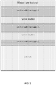
- FIG. 1 shows an embodiment of a monolithic multijunction power converter in which E 1 , E 2 , and E 3 represent semiconductor materials having the same bandgap.
- Each epitaxial layer has the same bandgap, which is roughly matched to the energy of the monochromatic light source to minimize minority carrier and thermal losses.
- the light source reaches the uppermost epitaxial layer furthest from the substrate.
- the epitaxial layer material may be a dilute-nitride material, such as GaInNAs or GaInNAsSb, or other dilute nitride known in the art.
- the monochromatic light source is between 1 micron and up to 1.55 microns, and in certain embodiments, the light source is approximately 1.3 microns. While some current may be lost through light absorption by the tunnel junction(s), light that is not collected in the first epitaxial layer is collected in the second epitaxial layer, and so on.
- the overall efficiency of such a device may reach at least 50% power efficiency, such as from 50% to 60% or from 50% to 70%.
- the power conversion efficiency of a single junction power converter is at least 20% such as from 20% to 40%.
- the power conversion efficiency of a single junction power converter is at least 30% such as from 30% to 50%.
- three junction devices provided by the present disclosure exhibit a conversion efficiency from about 23% to about 25% over an input power from about 0.6 W to about 6 W when irradiated with 1.32 micron radiation.
- three or more epitaxial layers of the same semiconductor material grown on a substrate such as GaInNAs, GaInNAsSb, GaAs, Ge, GaSb, InP or other substrate known in the art, are stacked on top of one another with tunnel junctions in between each epitaxial layer.
- a substrate such as GaInNAs, GaInNAsSb, GaAs, Ge, GaSb, InP or other substrate known in the art.
- Voc open circuit voltage
- Jsc short circuit current
- Each epitaxial layer has the same bandgap, which is roughly matched to the energy of the monochromatic light source to minimize minority carrier and thermal losses.
- the light source reaches the bottom most epitaxial layer closet to the substrate first.
- the substrate has a bandgap that is higher than the bandgap of the epitaxial layers. Given that the substrate has a higher bandgap than that of the epitaxial layers, the light source passes through the substrate and the light is absorbed by the epitaxial layers.
- An example of this employs GaInNAs epitaxial layers (bandgap of 0.95eV) and a GaAs substrate (bandgap 1.42eV). The light source in this example will not be absorbed by the GaAs substrate and will be absorbed by the GaInNAs active region.
- a heat sink can be coupled to the top of the uppermost epitaxial layer, and can serve to cool the device and prevent defects caused by overheating.
- the epitaxial layer material may be a dilute-nitride material, such as GaInNAs or GaInNAsSb, or other dilute nitride known in the art.
- the monochromatic light source has a wavelength between 1 micron and up to 1.55 microns, in certain embodiments, from 1 micron to 1.4 micron, and in certain embodiments the light source is approximately 1.3 microns. While some current may be lost through light absorption by the tunnel junction(s), light that is not collected in the first epitaxial layer can becollected in the second epitaxial layer, and so on. The overall efficiency of such a device may reach at least 50% power efficiency.
- the light absorbing layer(s) comprise GaInNAsSb.
- a GaInNAsSb junction comprises Ga 1-x In x N y As 1-y-z Sb z , in which values for x, y, and z are 0 ⁇ x ⁇ 0.24, 0.01 ⁇ y ⁇ 0.07 and 0.001 ⁇ z ⁇ 0.20; in certain embodiments, 0.02 ⁇ x ⁇ 0.24, 0.01 ⁇ y ⁇ 0.07 and 0.001 ⁇ z ⁇ 0.03; in certain embodiments, 0.02 ⁇ x ⁇ 0.18, 0.01 ⁇ y ⁇ 0.04 and 0.001 ⁇ z ⁇ 0.03; in certain embodiments, 0.08 ⁇ x ⁇ 0.18, 0.025 ⁇ y ⁇ 0.04 and 0.001 ⁇ z ⁇ 0.03; and in certain embodiments, 0.06 ⁇ x ⁇ 0.20, 0.02 ⁇ y ⁇ 0.05 and 0.005
- a GaInNAsSb junction comprises Ga 1-x In x N y As 1-y-z Sb z , in which values for x, y, and z are 0 ⁇ x ⁇ 0.18, 0.001 ⁇ y ⁇ 0.05 and 0.001 ⁇ z ⁇ 0.15, and in certain embodiments, 0 ⁇ x ⁇ 0.18, 0.001 ⁇ y ⁇ 0.05 and 0.001 ⁇ z ⁇ 0.03; in certain embodiments, 0.02 ⁇ x ⁇ 0.18, 0.005 ⁇ y ⁇ 0.04 and 0.001 ⁇ z ⁇ 0.03; in certain embodiments, 0.04 ⁇ x ⁇ 0.18, 0.01 ⁇ y ⁇ 0.04 and 0.001 ⁇ z ⁇ 0.03; in certain embodiments, 0.06 ⁇ x ⁇ 0.18, 0.015 ⁇ y ⁇ 0.04 and 0.001 ⁇ z ⁇ 0.03; and in certain embodiments, 0.08 ⁇
- a GaInNAsSb junction is characterized by a bandgap of 0.92 eV and comprises Ga 1-x In x N y As 1-y-z Sb z , in which values for x, y, and z are: x is 0.175, y is 0.04, and 0.012 ⁇ z ⁇ 0.019.
- a GaInNAsSb junction is characterized by a bandgap of 0.90 eV and comprises Ga 1-x In x N y As 1-y-z Sb z , in which values for x, y, and z are: x is 0.18, y is 0.045, and 0.012 ⁇ z ⁇ 0.019.
- a GaInNAsSb junction is comprises Ga 1-x In x N y As 1-y-z Sb z , in which values for x, y, and z are: 0.13 ⁇ x ⁇ 0.19, 0.03 ⁇ y ⁇ 0.048, and 0.007 ⁇ z ⁇ 0.02.
- a GaInNAsSb junction comprises Ga 1-x In x N y As 1-y-z Sb z , in which values for x, y, and z are selected to have a band gap that matches or closely matches the energy of the radiation used to deliver power to the device.
- the GaInNAsSb junction is substantially lattice matched to a GaAs substrate. It is to be noted that the general understanding of "substantially lattice matched" is that the in-plane lattice constants of the materials in their fully relaxed states differ by less than 0.6% when the materials are present in thicknesses greater than 100 nm.
- subcells that are substantially lattice matched to each other as used herein means that all materials in the subcells that are present in thicknesses greater than 100 nm have in-plane lattice constants in their fully relaxed states that differ by less than 0.6%.
- each of the epitaxial layers in the power converter is lattice matched to a GaAs substrate.
- the use of layering materials of different refractive indices can produce distributed Bragg reflectors (DBR) within the structure and is used to increase the efficiency of the power converter.
- DBR distributed Bragg reflectors
- a dilute nitride material which in certain embodiments is a GaInNAsSb material, as the absorbing material in the epitaxial stack of the structure.
- a cavity can be grown using a material such as GaAs / AlGaAs as a DBR below the dilute nitride layer and above the substrate, and another DBR grown above the dilute nitride layer, that can be made of semiconductors or a number of oxides.
- a back-side metal can be used as structured mirror, allowing unabsorbed light to be reflected from the back metal to be reabsorbed in the epitaxial layers above.
- FIGS. 2A and 2B Examples of resonant cavity power converters using the double pass configuration are shown in FIGS. 2A and 2B.
- FIG. 2A shows a single junction resonant cavity with a top DBR and a bottom DBR.
- a single GaInNAsSb junction is disposed between the two DBRs and separated from the DBRs by semiconductor layers d1 and d2.
- Semiconductor layers may be formed from a material that does not appreciably absorb the incident radiation and that can be lattice matched to GaAs and the absorbing layer, and in certain embodiments are GaAs.
- the thickness of d1, d2 and a GaInNAsSb junction can be selected to provide a standing wave at the wavelength of the incident radiation.
- FIG. 2B shows a similar configuration as shown in FIG. 2A but includes multiple GaInNAsSb junctions with each of the junctions separated by a tunnel junction.
- the thickness of the GaInNAsSb junction is from about 100 nm to about 1 micron.
- the substrate is a semi-insulating or n-doped GaAs substrate with a back-metal as the bottom-most layer of the structure.
- the mirror layer can be, for example, gold or gold/nickel alloys.
- the power converter structure uses one DBR instead of two.
- Resonant power converters employing a single DBR are shown in FIGS. 3A and 3B.
- FIG. 3A shows a single GaInNAsSb junction disposed between two semiconductor layers d1 and d2. These layers overly a bottom DBR, which overlies a substrate.
- the upper surface of the device, such as the upper surface of layer d1 facing the incident radiation may be coated with an antireflection coating.
- the antireflection coating may be optimized for the wavelength of the incident radiation to reduce scatteing.
- FIG. 3B shows a single DBR resonant cavity configuration having multiple GaInNAsSb junctions.
- the power converter structure includes one DBR and a back mirror below the substrate.
- DBR Downlink Biharmonic Device
- FIGS. 4A, 4B , 5A, and 5B show power converters having a top DBR a resonant cavity including a single GaInNAsSb junction between two semiconductor layers d1 and d2, and a back mirror beneath semiconductor layer d2.
- the back mirror can also serve as an electrical contact.
- a multi-junction power converter is shown in FIG. 4B in which multiple GaInNAsSb junctions are disposed between a top DBR and a back mirror.
- both a DBR and a back mirror are used at the bottom of the device.
- the thickness of the DBR can be reduced compared to a configuration with a bottom DBR without the back mirror.
- the upper surface of layer D1 may include an antireflection coating.
- the substrate is removed and a metal is used it its place as a back mirror. In such structures, the light passes through the top DBR, then through the epitaxial layers, then through the bottom DBR and finally hits the back mirror.
- the epitaxial layer comprises GaInNAsSb as one or more absorbing layers.
- the upper most layer of the structure comprises an interface air-semiconductor above the epitaxial layers, which may comprise of one or more layers of GaInNAsSb.
- a bottom DBR which overlays a back mirror.
- the substrate can be GaAs such as n-type GaAs and can have a thickness from about 150 microns to about 250 microns, such as from 175 microns to 225 microns.
- the thickness of the substrate can be thinned, for example, by grinding or etching to minimize absorption and in such embodiments can be 50 microns or less.
- the bottom DBR can be bonded to a heatsink. Bonding the DBR directly to the heatsink can reduce the temperature of the power converter.
- FIGS. 7A and 7B shown device configurations similar to those shown in FIGS. 6A and 6B but with the bottom DBR replaced with a back mirror.
- the structure has intra-cavity contacts to avoid resistivity from the DBR structures.
- the contact is made in the cavity through lateral transport conducting layers (LCL) bypassing the DBR structures.
- Power converters having intra-cavity contacts are shown in FIGS. 8A and 8B .
- the epitaxial layers are etched down to either an LCL overlying the bottom DBR or to an LCL overlying semiconductor layer d1.
- the LCLs improve carrier mobility to the electrical contacts (back contact and top contact) and can be formed, for example, from doped GaAs such as n-type GaAs. LCLs and similar etch back electrical contacts can be employed with other device structures provided by the present disclosure.
- the structure can be grown inverted.
- the substrate can be thinned down to a certain thickness or removed after growth using a variety of lift off techniques.
- the light passes through the substrate first before passing through the epitaxy layers.
- the bandgap of the substrate is greater than the bandgap of the epitaxial layers.
- Multiple photovoltaic converters comprised of a number of subcells connected in series can be constructed to increase the output voltage.
- the subcells can be connected in parallel for increasing output current.
- An example is a Pi structure as shown in FIG. 9 .
- Infrared absorbers are typically characterized by low voltage; however, in certain application it is desirable to increase the voltage of the power converter. This can be accomplished by connecting multiple power converters in series.
- One such configuration, of which a top-down view is shown in FIG. 9 is referred to as a pie structure in which multiple power converter cells are disposed in concentric rings around a central axis, where each cell is separated by an insulator and the multiple cells or subsets of the multiple cells are connected in series.
- Such structures can be fabricated using single junctions and provide a high density of cells.
- the higher voltages provide improved DC-DC converter efficiencies and lower Ohmic losses.
- later currents can produce Ohmic losses this can be offset because the increased number of sub-cells results in lower currents.
- FIGS. 10A and 10B Other device structures are shown in FIGS. 10A and 10B.
- FIG. 10A shows single a triple-junction double pass power converter.
- FIG. 10B shows a four quadrant triple-junction double pass power converter.
- the dimensions of the devices are 300 microns by 300 microns.
- the four converters can be interconnected in series to increase the voltage and/or decrease the current.
- the series interconnection can also reduce the sensitivity to spatial orientation of the incident radiation.
- separating the collection area into quadrants or other sub-areas can reduce the Ohmic losses by bringing the electrical contacts closer to the power generating surfaces. Photographs of the single and four quadrant devices are shown in FIGS. 11A and 11B .
- the power converters shown in FIGS. 10A, 10B , 11A, and 11B were fabricated using GaInNAsSb junctions. All epitaxial layers were lattice matched to a GaAs substrate. A back mirror is disposed at the bottom of the GaAs substrate. The resonant cavity of the three-junction structures was configured to support a standing wave at about 1.3 microns, such as at 1.32 microns or at1.342 microns. The bandgap of the GaInNAsSb junctions was about 0.92 eV for devices configured for power conversion at 1.32 microns.
- Certain of such devices exhibited a fill factor from about 65% to about 75%, a Voc of from about 1.4 7V to about 1.5 V and a Jsc from about 0.6 A to about 1.4 A.
- the power conversion efficiency was from about 23% to 25% at an input power from about 0.6 W to about 6 W.
- the two or more epitaxial layers of the same semiconductor material are of varying thicknesses.
- the epitaxial layers can decrease in thickness the further away from the light source.
- the thicknesses of each of the epitaxial layers are the same.
- the thicknesses of the epitaxial layers are varied, either increasing nor decreasing depending on the light source location.
- the thickness, or height, of the entire device may be between 1 micron and up to 10 microns.
- the area of the power converter can be, for example, between 100 microns ⁇ 100 microns, and up to 1 cm ⁇ 1 cm, or more. For example the total area is from 10 -4 cm 2 to 1 cm 2 .
- the thickness of each epitaxial layer may be between a few hundred nanometers up to a few microns.
- FIG. 12 shows the efficiency, power output and voltage at maximum power point (Mpp) as a function of laser input power for single (open circle), double (square), and triple (plus) GaInNAsSb junction power converters.
- FIG. 13 shows the normalized current density (J) as a function of voltage for several laser input power levels for single (open circle), double (square), and triple (plus) GaInNAsSb junction power converters.
Landscapes
- Life Sciences & Earth Sciences (AREA)
- Semiconductor Lasers (AREA)
- Sustainable Development (AREA)
- Engineering & Computer Science (AREA)
- Sustainable Energy (AREA)
- Photovoltaic Devices (AREA)
Description
- The disclosure relates to the field of power conversion.
- Power converters may be used in a number of applications to charge electronic devices, such as cell phones, audio systems, home theaters, or any other electronic devices, from a power source. It is well known in the field that Ohmic losses are inversely related to an increase in voltage and directly related to an increase in current. It is advantageous, then, to increase the fill factor of power converter devices by increasing the voltage of the devices.
- Prior art power converters in the field include monolithically series-connected single layer converters made of semiconductor wafers, such as GaAs. Such power converters may be connected in series by wiring or sectored off by manufacturing the converter on a semi-insulating substrate using insulating trenches to provide electrical insulation between each sectored converter. The energy source for such power converters is a monochromatic light, such as a laser operating at a particular wavelength or energy. In this particular application, the monochromatic light is between 1 micron to 1.55 microns, in the infrared region of the spectrum. Closer to 1 micron is less advantageous for home use due to the potential dangers of the light source to the human eye, so the focus of the embodiments disclosed herein is on light sources between 1.3-1.55 microns, and in certain embodiments, around 1.3 microns. However, those skilled in the field may easily modify the invention disclosed herein to convert light of a number of wavelengths. The following documents are part of the prior art relevant to the invention:
US2010/116318A1 ,US2012/153417A1 , ANDREEV et al: "High current density GaAs and GaSb photovoltaic cells for laser power beaming", PROCEEDINGS OF THE 3RD WORLD CONFERENCE ON PHOTOVOLTAIC ENERGY CONVERSION, 18 May 2003, pages 761-764 and SCHUBERT et al: "High-Voltage GaAs Photovoltaic Laser Power Converters", IEEE TRANSACTIONS ON ELECTRON DEVICES,vol. 56, no. 2, February 2009, pages 170-175. - The invention comprises a compact, monolithic multijunction power converter, with two or more epitaxial layers of the same material stacked on top of one another with tunnel junctions in between each epitaxial layer. Because the epitaxial layers are stacked on top of one another, each epitaxial layer is thinned to collect a maximum amount of light and converts power in series to increase the fill factor by increasing voltage of the overall device and decreasing Ohmic losses (which increase with current increase). Given the stacked epitaxial layers, light which is not absorbed in one layer is absorbed in the next layer directly beneath the first layer and so on. The power converter may reach an overall efficiency of approximately 50%. There are minimal current losses in these devices given that complex circuitry is avoided using the vertical stacking of the epitaxial layers, compared to the prior art, which requires interconnections between the semiconductor light absorbing sectors.
- The subject-matter of the present invention is defined in independent claim 1. Particular embodiments of the invention provide resonant cavity laser power converters as set out in the appended dependent claims.
- The drawings described herein are for illustration purposes only. The drawings are not intended to limit the scope of the present disclosure.
Figures 2B ,6B and8B show embodiments of the invention.Figures 1 ,2A ,3A, 3B ,4A, 4B ,5A, 5B ,6A ,7A, 7B and8A show embodiments not being part of the invention. -
FIG. 1 shows an embodiment of a monolithic multijunction power converter in which E1, E2, and E3 represent semiconductor materials having the same bandgap. -
FIGS. 2A and 2B show single junction and triple junction resonant power converters, respectively, with dual distributed Bragg reflectors (DBR), according to certain embodiments. -
FIGS. 3A and 3B show single junction and triple junction resonant power converters, respectively, with single DBRs, according to certain embodiments. -
FIGS. 4A and 4B show single junction and triple junction resonant power converters, respectively, with a top DBR and a back mirror, according to certain embodiments. -
FIGS. 5A and 5B show single junction and triple junction resonant power converters, respectively, with a back mirror, according to certain embodiments. -
FIGS. 6A and 6B show single junction and triple junction resonant power converters, respectively, with two DBRs and a top substrate, according to certain embodiments. -
FIGS. 7A and8B show single junction and triple junction resonant power converters, respectively, with a substrate overlying a top DBR and a back mirror, according to certain embodiments. -
FIGS. 8A and 8B show single junction and triple junction resonant power converters, respectively, with two DBRs and etched back contacts to lateral conducting layers (LCL), according to certain embodiments. -
FIG. 9 shows a top view of a pie structure having multiple power converters interconnected in series, according to certain embodiments. -
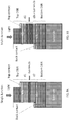
FIGS. 10A and 10B show triple-junction power converters having a double pass configuration and characterized by a single area (FIG. 10A ) or four quadrant area (FIG. 10B ), according to certain embodiments. -
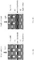
FIGS. 11A and 11B show photographs of the top view of the triple-junction power converters shown schematically inFIGS. 10A and 10B , respectively. -
FIG. 12 shows the efficiency, power output, and voltage at maximum power point (Mpp) as a function of laser input power for single, double, and triple lattice-matched GaInNAsSb junction power converters. -
FIG. 13 shows the normalized density of current (J) as a function of voltage for several laser input power levels for single, double and triple lattice-matched GaInNAsSb junction power converters. - Reference is now made in detail to embodiments of the present disclosure. While certain embodiments of the present disclosure are described, it will be understood that it is not intended to limit the embodiments of the present disclosure to the disclosed embodiments. To the contrary, reference to embodiments of the present disclosure is intended to cover alternatives, modifications, and equivalents as may be included within the spirit and scope of the embodiments of the present disclosure as defined by the appended claims.
- In certain embodiments provided by the present disclosure, two or more epitaxial layers of the same semiconductor material grown on a substrate, such as GaInNAs, GaInNAsSb, GaAs, Ge, GaSb, InP or other substrate known in the art, are stacked on top of one another with tunnel junctions in between each epitaxial layer.
FIG. 1 shows an embodiment of a monolithic multijunction power converter in which E1, E2, and E3 represent semiconductor materials having the same bandgap. Each epitaxial layer has the same bandgap, which is roughly matched to the energy of the monochromatic light source to minimize minority carrier and thermal losses. In certain embodiments, the light source reaches the uppermost epitaxial layer furthest from the substrate. In some embodiments, the epitaxial layer material may be a dilute-nitride material, such as GaInNAs or GaInNAsSb, or other dilute nitride known in the art. In some embodiments, the monochromatic light source is between 1 micron and up to 1.55 microns, and in certain embodiments, the light source is approximately 1.3 microns. While some current may be lost through light absorption by the tunnel junction(s), light that is not collected in the first epitaxial layer is collected in the second epitaxial layer, and so on. The overall efficiency of such a device may reach at least 50% power efficiency, such as from 50% to 60% or from 50% to 70%. In certain embodiments, the power conversion efficiency of a single junction power converter is at least 20% such as from 20% to 40%. In certain embodiments, the power conversion efficiency of a single junction power converter is at least 30% such as from 30% to 50%. In certain embodiments, three junction devices provided by the present disclosure exhibit a conversion efficiency from about 23% to about 25% over an input power from about 0.6 W to about 6 W when irradiated with 1.32 micron radiation. - In certain embodiments, three or more epitaxial layers of the same semiconductor material grown on a substrate such as GaInNAs, GaInNAsSb, GaAs, Ge, GaSb, InP or other substrate known in the art, are stacked on top of one another with tunnel junctions in between each epitaxial layer. Increasing the number of junctions in a power converter device can result in increased fill factor, increased open circuit voltage (Voc) and decreased short circuit current (Jsc). Each epitaxial layer has the same bandgap, which is roughly matched to the energy of the monochromatic light source to minimize minority carrier and thermal losses. In certain embodiments, the light source reaches the bottom most epitaxial layer closet to the substrate first. The substrate has a bandgap that is higher than the bandgap of the epitaxial layers. Given that the substrate has a higher bandgap than that of the epitaxial layers, the light source passes through the substrate and the light is absorbed by the epitaxial layers. An example of this employs GaInNAs epitaxial layers (bandgap of 0.95eV) and a GaAs substrate (bandgap 1.42eV). The light source in this example will not be absorbed by the GaAs substrate and will be absorbed by the GaInNAs active region. A heat sink can be coupled to the top of the uppermost epitaxial layer, and can serve to cool the device and prevent defects caused by overheating. In some embodiments, the epitaxial layer material may be a dilute-nitride material, such as GaInNAs or GaInNAsSb, or other dilute nitride known in the art. In some embodiments, the monochromatic light source has a wavelength between 1 micron and up to 1.55 microns, in certain embodiments, from 1 micron to 1.4 micron, and in certain embodiments the light source is approximately 1.3 microns. While some current may be lost through light absorption by the tunnel junction(s), light that is not collected in the first epitaxial layer can becollected in the second epitaxial layer, and so on. The overall efficiency of such a device may reach at least 50% power efficiency.
- In certain embodiments, the light absorbing layer(s) comprise GaInNAsSb. In certain of the embodiments, a GaInNAsSb junction comprises Ga1-xInxNyAs1-y-zSbz, in which values for x, y, and z are 0 ≤ x ≤ 0.24, 0.01 ≤ y ≤ 0.07 and 0.001 ≤ z ≤ 0.20; in certain embodiments, 0.02 ≤ x ≤ 0.24, 0.01 ≤ y ≤ 0.07 and 0.001 ≤ z ≤ 0.03; in certain embodiments, 0.02 ≤ x ≤ 0.18, 0.01 ≤ y ≤ 0.04 and 0.001 ≤ z ≤ 0.03; in certain embodiments, 0.08 ≤ x ≤ 0.18, 0.025≤ y ≤ 0.04 and 0.001 ≤ z ≤ 0.03; and in certain embodiments, 0.06 ≤ x ≤ 0.20, 0.02 ≤ y ≤ 0.05 and 0.005 ≤ z ≤ 0.02.
- In certain of the embodiments, a GaInNAsSb junction comprises Ga1-xInxNyAs1-y-zSbz, in which values for x, y, and z are 0 ≤ x ≤ 0.18, 0.001 ≤ y ≤ 0.05 and 0.001 ≤ z ≤ 0.15, and in certain embodiments, 0 ≤ x ≤ 0.18, 0.001 ≤ y ≤ 0.05 and 0.001 ≤ z ≤ 0.03; in certain embodiments, 0.02 ≤ x ≤ 0.18, 0.005 ≤ y ≤ 0.04 and 0.001 ≤ z ≤ 0.03; in certain embodiments, 0.04 ≤ x ≤ 0.18, 0.01 ≤ y ≤ 0.04 and 0.001 ≤ z ≤ 0.03; in certain embodiments, 0.06 ≤ x ≤ 0.18, 0.015≤ y ≤ 0.04 and 0.001 ≤ z ≤ 0.03; and in certain embodiments, 0.08 ≤ x ≤ 0.18, 0.025≤ y ≤ 0.04 and 0.001 ≤ z ≤ 0.03.
- In certain embodiments, a GaInNAsSb junction is characterized by a bandgap of 0.92 eV and comprises Ga1-xInxNyAs1-y-zSbz, in which values for x, y, and z are: x is 0.175, y is 0.04, and 0.012 ≤ z ≤ 0.019.
- In certain embodiments, a GaInNAsSb junction is characterized by a bandgap of 0.90 eV and comprises Ga1-xInxNyAs1-y-zSbz, in which values for x, y, and z are: x is 0.18, y is 0.045, and 0.012 ≤ z ≤ 0.019.
- In certain embodiments, a GaInNAsSb junction is comprises Ga1-xInxNyAs1-y-zSbz, in which values for x, y, and z are: 0.13 ≤ x ≤ 0.19, 0.03 ≤ y ≤ 0.048, and 0.007 ≤ z ≤ 0.02.
- In certain embodiments, a GaInNAsSb junction comprises Ga1-xInxNyAs1-y-zSbz, in which values for x, y, and z are selected to have a band gap that matches or closely matches the energy of the radiation used to deliver power to the device. In certain embodiments, the GaInNAsSb junction is substantially lattice matched to a GaAs substrate. It is to be noted that the general understanding of "substantially lattice matched" is that the in-plane lattice constants of the materials in their fully relaxed states differ by less than 0.6% when the materials are present in thicknesses greater than 100 nm. Further, subcells that are substantially lattice matched to each other as used herein means that all materials in the subcells that are present in thicknesses greater than 100 nm have in-plane lattice constants in their fully relaxed states that differ by less than 0.6%.
- In certain embodiments, each of the epitaxial layers in the power converter is lattice matched to a GaAs substrate.
- In certain embodiments, the use of layering materials of different refractive indices can produce distributed Bragg reflectors (DBR) within the structure and is used to increase the efficiency of the power converter. One such example uses a dilute nitride material, which in certain embodiments is a GaInNAsSb material, as the absorbing material in the epitaxial stack of the structure. A cavity can be grown using a material such as GaAs / AlGaAs as a DBR below the dilute nitride layer and above the substrate, and another DBR grown above the dilute nitride layer, that can be made of semiconductors or a number of oxides.
- In certain embodiments, where the substrate has a higher bandgap than the absorbing material, a back-side metal can be used as structured mirror, allowing unabsorbed light to be reflected from the back metal to be reabsorbed in the epitaxial layers above. Examples of resonant cavity power converters using the double pass configuration are shown in
FIGS. 2A and 2B. FIG. 2A shows a single junction resonant cavity with a top DBR and a bottom DBR. A single GaInNAsSb junction is disposed between the two DBRs and separated from the DBRs by semiconductor layers d1 and d2. Semiconductor layers may be formed from a material that does not appreciably absorb the incident radiation and that can be lattice matched to GaAs and the absorbing layer, and in certain embodiments are GaAs. The thickness of d1, d2 and a GaInNAsSb junction can be selected to provide a standing wave at the wavelength of the incident radiation.FIG. 2B shows a similar configuration as shown inFIG. 2A but includes multiple GaInNAsSb junctions with each of the junctions separated by a tunnel junction. The thickness of the GaInNAsSb junction is from about 100 nm to about 1 micron. In certain embodiments, the substrate is a semi-insulating or n-doped GaAs substrate with a back-metal as the bottom-most layer of the structure. - For use with 1 micron to 1.55 micron radiation, the mirror layer can be, for example, gold or gold/nickel alloys.
- In certain embodiments, the power converter structure uses one DBR instead of two. Resonant power converters employing a single DBR are shown in
FIGS. 3A and 3B. FIG. 3A shows a single GaInNAsSb junction disposed between two semiconductor layers d1 and d2. These layers overly a bottom DBR, which overlies a substrate. The upper surface of the device, such as the upper surface of layer d1 facing the incident radiation may be coated with an antireflection coating. The antireflection coating may be optimized for the wavelength of the incident radiation to reduce scatteing.FIG. 3B shows a single DBR resonant cavity configuration having multiple GaInNAsSb junctions. - In certain embodiments, the power converter structure includes one DBR and a back mirror below the substrate. Such device configurations are shown in
FIGS. 4A, 4B ,5A, and 5B .FIGS. 4A and 4B show power converters having a top DBR a resonant cavity including a single GaInNAsSb junction between two semiconductor layers d1 and d2, and a back mirror beneath semiconductor layer d2. In certain embodiments, the back mirror can also serve as an electrical contact. A multi-junction power converter is shown inFIG. 4B in which multiple GaInNAsSb junctions are disposed between a top DBR and a back mirror. - In the power converters shown in
FIGS. 5A and 5B both a DBR and a back mirror are used at the bottom of the device. In this configuration the thickness of the DBR can be reduced compared to a configuration with a bottom DBR without the back mirror. As with other devices, the upper surface of layer D1 may include an antireflection coating. In certain embodiments, the substrate is removed and a metal is used it its place as a back mirror. In such structures, the light passes through the top DBR, then through the epitaxial layers, then through the bottom DBR and finally hits the back mirror. In these embodiments, the epitaxial layer comprises GaInNAsSb as one or more absorbing layers. - In certain embodiments, the upper most layer of the structure comprises an interface air-semiconductor above the epitaxial layers, which may comprise of one or more layers of GaInNAsSb. Below the epitaxial layer is a bottom DBR which overlays a back mirror. In these embodiments, the light hits the upper most layer of the interface air-semiconductor and moves to the epitaxial layer, then the DBR and finally reflects back through the structure after being reflected by the back mirror.
- Resonant cavity configurations with two DBRs and a top substrate layer are shown in
FIGS. 6A and 6B . The top substrate layer is substantially transparent to the incident radiation used to generate the power. In certain embodiments, the substrate can be GaAs such as n-type GaAs and can have a thickness from about 150 microns to about 250 microns, such as from 175 microns to 225 microns. The thickness of the substrate can be thinned, for example, by grinding or etching to minimize absorption and in such embodiments can be 50 microns or less. In certain embodiments, the bottom DBR can be bonded to a heatsink. Bonding the DBR directly to the heatsink can reduce the temperature of the power converter. -
FIGS. 7A and 7B shown device configurations similar to those shown inFIGS. 6A and 6B but with the bottom DBR replaced with a back mirror. - In certain embodiments, the structure has intra-cavity contacts to avoid resistivity from the DBR structures. The contact is made in the cavity through lateral transport conducting layers (LCL) bypassing the DBR structures. Power converters having intra-cavity contacts are shown in
FIGS. 8A and 8B . In these device structures the epitaxial layers are etched down to either an LCL overlying the bottom DBR or to an LCL overlying semiconductor layer d1. The LCLs improve carrier mobility to the electrical contacts (back contact and top contact) and can be formed, for example, from doped GaAs such as n-type GaAs. LCLs and similar etch back electrical contacts can be employed with other device structures provided by the present disclosure. - In certain embodiments, the structure can be grown inverted. In such cases, the substrate can be thinned down to a certain thickness or removed after growth using a variety of lift off techniques. The light passes through the substrate first before passing through the epitaxy layers. In such structures, the bandgap of the substrate is greater than the bandgap of the epitaxial layers.
- Multiple photovoltaic converters comprised of a number of subcells connected in series can be constructed to increase the output voltage. The subcells can be connected in parallel for increasing output current. An example is a Pi structure as shown in
FIG. 9 . Infrared absorbers are typically characterized by low voltage; however, in certain application it is desirable to increase the voltage of the power converter. This can be accomplished by connecting multiple power converters in series. One such configuration, of which a top-down view is shown inFIG. 9 , is referred to as a pie structure in which multiple power converter cells are disposed in concentric rings around a central axis, where each cell is separated by an insulator and the multiple cells or subsets of the multiple cells are connected in series. Such structures can be fabricated using single junctions and provide a high density of cells. The higher voltages provide improved DC-DC converter efficiencies and lower Ohmic losses. Although later currents can produce Ohmic losses this can be offset because the increased number of sub-cells results in lower currents. - Other device structures are shown in
FIGS. 10A and 10B. FIG. 10A shows single a triple-junction double pass power converter.FIG. 10B shows a four quadrant triple-junction double pass power converter. The dimensions of the devices are 300 microns by 300 microns. The four converters can be interconnected in series to increase the voltage and/or decrease the current. The series interconnection can also reduce the sensitivity to spatial orientation of the incident radiation. Furthermore, for large area power converters, separating the collection area into quadrants or other sub-areas can reduce the Ohmic losses by bringing the electrical contacts closer to the power generating surfaces. Photographs of the single and four quadrant devices are shown inFIGS. 11A and 11B . - The power converters shown in
FIGS. 10A, 10B ,11A, and 11B were fabricated using GaInNAsSb junctions. All epitaxial layers were lattice matched to a GaAs substrate. A back mirror is disposed at the bottom of the GaAs substrate. The resonant cavity of the three-junction structures was configured to support a standing wave at about 1.3 microns, such as at 1.32 microns or at1.342 microns. The bandgap of the GaInNAsSb junctions was about 0.92 eV for devices configured for power conversion at 1.32 microns. Certain of such devices exhibited a fill factor from about 65% to about 75%, a Voc of from about 1.4 7V to about 1.5 V and a Jsc from about 0.6 A to about 1.4 A. The power conversion efficiency was from about 23% to 25% at an input power from about 0.6 W to about 6 W. - In certain embodiments, the two or more epitaxial layers of the same semiconductor material are of varying thicknesses. In particular, the epitaxial layers can decrease in thickness the further away from the light source. In certain embodiments, the thicknesses of each of the epitaxial layers are the same. In certain embodiments, the thicknesses of the epitaxial layers are varied, either increasing nor decreasing depending on the light source location.
- In some embodiments, there is a window layer on top of the upper most epitaxial layer.
- In certain embodiments, the thickness, or height, of the entire device may be between 1 micron and up to 10 microns. The area of the power converter can be, for example, between 100 microns × 100 microns, and up to 1 cm × 1 cm, or more. For example the total area is from 10-4 cm2 to 1 cm2. The thickness of each epitaxial layer may be between a few hundred nanometers up to a few microns.
-
FIG. 12 shows the efficiency, power output and voltage at maximum power point (Mpp) as a function of laser input power for single (open circle), double (square), and triple (plus) GaInNAsSb junction power converters. -
FIG. 13 shows the normalized current density (J) as a function of voltage for several laser input power levels for single (open circle), double (square), and triple (plus) GaInNAsSb junction power converters.
Claims (3)
- A resonant cavity laser power converter, comprising:a bottom distributed Bragg reflector;a first semiconductor layer overlying the bottom distributed Bragg reflector;multiple GaInNAsSb junctions overlying the first semiconductor layer with each of the junctions is separated by a tunnel junction, wherein each of the multiple GaInNASb junctions has a thickness from about 100 nm to about 1 micron;a second semiconductor layer overlying the multiple GaInNAsSb junctions; anda top distributed Bragg reflector overlying the second semiconductor layer,wherein each of the first semiconductor layer and the second semiconductor layer is GaAs.
- The resonant cavity laser power converter of claim 1, wherein the thickness of the first semiconductor layer, the second semiconductor layer and the GaInNAsSb junctions are selected to provide a standing wave at an incident wavelength.
- The resonant cavity laser power converter of claim 1, wherein each of the first and second semiconductor layers is lattice matched to the GaInNAsSb layers.
Priority Applications (1)
| Application Number | Priority Date | Filing Date | Title |
|---|---|---|---|
| EP20191506.3A EP3761375A1 (en) | 2014-02-05 | 2015-02-05 | Monolithic multijunction power converter |
Applications Claiming Priority (2)
| Application Number | Priority Date | Filing Date | Title |
|---|---|---|---|
| US201461936222P | 2014-02-05 | 2014-02-05 | |
| PCT/US2015/014650 WO2015120169A1 (en) | 2014-02-05 | 2015-02-05 | Monolithic multijunction power converter |
Related Child Applications (1)
| Application Number | Title | Priority Date | Filing Date |
|---|---|---|---|
| EP20191506.3A Division EP3761375A1 (en) | 2014-02-05 | 2015-02-05 | Monolithic multijunction power converter |
Publications (2)
| Publication Number | Publication Date |
|---|---|
| EP3103142A1 EP3103142A1 (en) | 2016-12-14 |
| EP3103142B1 true EP3103142B1 (en) | 2020-08-19 |
Family
ID=52472636
Family Applications (2)
| Application Number | Title | Priority Date | Filing Date |
|---|---|---|---|
| EP15704681.4A Not-in-force EP3103142B1 (en) | 2014-02-05 | 2015-02-05 | Monolithic multijunction power converter |
| EP20191506.3A Withdrawn EP3761375A1 (en) | 2014-02-05 | 2015-02-05 | Monolithic multijunction power converter |
Family Applications After (1)
| Application Number | Title | Priority Date | Filing Date |
|---|---|---|---|
| EP20191506.3A Withdrawn EP3761375A1 (en) | 2014-02-05 | 2015-02-05 | Monolithic multijunction power converter |
Country Status (8)
| Country | Link |
|---|---|
| US (4) | US20150221803A1 (en) |
| EP (2) | EP3103142B1 (en) |
| CN (2) | CN106133923B (en) |
| ES (1) | ES2831831T3 (en) |
| SA (1) | SA516371606B1 (en) |
| SG (1) | SG11201606353TA (en) |
| TW (1) | TWI656651B (en) |
| WO (1) | WO2015120169A1 (en) |
Families Citing this family (17)
| Publication number | Priority date | Publication date | Assignee | Title |
|---|---|---|---|---|
| MX337295B (en) | 2009-02-09 | 2016-02-23 | Semprius Inc | MODULES, RECEPTORS AND PHOTOVOLTAIC SUB-RECEIVERS CONCENTRATOR TYPE AND METHODS TO FORM THE SAME. |
| CN106133923B (en) | 2014-02-05 | 2018-07-24 | 太阳结公司 | Monolithic Multijunction Energy Converter |
| DE102015012007A1 (en) * | 2015-09-19 | 2017-03-23 | Azur Space Solar Power Gmbh | Scalable voltage source |
| US20170110613A1 (en) * | 2015-10-19 | 2017-04-20 | Solar Junction Corporation | High efficiency multijunction photovoltaic cells |
| DE102016013749A1 (en) * | 2016-11-18 | 2018-05-24 | Azur Space Solar Power Gmbh | Stack-shaped semiconductor structure |
| US10930808B2 (en) | 2017-07-06 | 2021-02-23 | Array Photonics, Inc. | Hybrid MOCVD/MBE epitaxial growth of high-efficiency lattice-matched multijunction solar cells |
| EP3669402A1 (en) | 2017-09-27 | 2020-06-24 | Array Photonics, Inc. | Short wavelength infrared optoelectronic devices having a dilute nitride layer |
| EP3766104A1 (en) * | 2018-03-12 | 2021-01-20 | Solar Junction Corporation | Chirped distributed bragg reflectors for photovoltaic cells and other light absorption devices |
| US10797197B2 (en) | 2018-06-18 | 2020-10-06 | Alta Devices, Inc. | Thin-film, flexible optoelectronic devices incorporating a single lattice-matched dilute nitride junction and methods of fabrication |
| EP3844816A4 (en) * | 2018-08-30 | 2022-05-18 | Array Photonics, Inc. | SOLAR CELLS WITH MULTIPLE JUNCTIONS AND MULTICOLOR PHOTOSENSORS WITH INTEGRATED MARGINAL FILTER |
| US11211514B2 (en) | 2019-03-11 | 2021-12-28 | Array Photonics, Inc. | Short wavelength infrared optoelectronic devices having graded or stepped dilute nitride active regions |
| US11575055B2 (en) | 2019-07-15 | 2023-02-07 | SLT Technologies, Inc | Methods for coupling of optical fibers to a power photodiode |
| US11569398B2 (en) | 2019-07-15 | 2023-01-31 | SLT Technologies, Inc | Power photodiode structures and devices |
| US11444216B2 (en) | 2019-07-15 | 2022-09-13 | Slt Technologies, Inc. | Power photodiode structures, methods of making, and methods of use |
| US11670735B2 (en) | 2020-12-14 | 2023-06-06 | Lumileds Llc | Monolithic electrical power converter formed with layers |
| CN118103996A (en) * | 2021-10-15 | 2024-05-28 | 艾迈斯-欧司朗国际有限责任公司 | Optoelectronic devices |
| JP2025007239A (en) * | 2023-06-30 | 2025-01-17 | 日本電信電話株式会社 | Photoelectric conversion element |
Family Cites Families (159)
| Publication number | Priority date | Publication date | Assignee | Title |
|---|---|---|---|---|
| US4127862A (en) | 1977-09-06 | 1978-11-28 | Bell Telephone Laboratories, Incorporated | Integrated optical detectors |
| US4179702A (en) | 1978-03-09 | 1979-12-18 | Research Triangle Institute | Cascade solar cells |
| US4404421A (en) | 1982-02-26 | 1983-09-13 | Chevron Research Company | Ternary III-V multicolor solar cells and process of fabrication |
| GB2132016B (en) | 1982-12-07 | 1986-06-25 | Kokusai Denshin Denwa Co Ltd | A semiconductor device |
| JPS6061513A (en) | 1983-09-14 | 1985-04-09 | Sansho Seiyaku Kk | Cosmetic |
| JPS6061516A (en) | 1983-09-14 | 1985-04-09 | Sansho Seiyaku Kk | The first solution for permanent wave |
| US4547622A (en) | 1984-04-27 | 1985-10-15 | Massachusetts Institute Of Technology | Solar cells and photodetectors |
| US4881979A (en) | 1984-08-29 | 1989-11-21 | Varian Associates, Inc. | Junctions for monolithic cascade solar cells and methods |
| JPS63100781A (en) | 1986-10-17 | 1988-05-02 | Nippon Telegr & Teleph Corp <Ntt> | Semiconductor element |
| US5016562A (en) | 1988-04-27 | 1991-05-21 | Glasstech Solar, Inc. | Modular continuous vapor deposition system |
| US4935384A (en) | 1988-12-14 | 1990-06-19 | The United States Of America As Represented By The United States Department Of Energy | Method of passivating semiconductor surfaces |
| JPH02218174A (en) | 1989-02-17 | 1990-08-30 | Mitsubishi Electric Corp | Photoelectric converting semiconductor device |
| US5223043A (en) | 1991-02-11 | 1993-06-29 | The United States Of America As Represented By The United States Department Of Energy | Current-matched high-efficiency, multijunction monolithic solar cells |
| US5166761A (en) | 1991-04-01 | 1992-11-24 | Midwest Research Institute | Tunnel junction multiple wavelength light-emitting diodes |
| US5330585A (en) | 1992-10-30 | 1994-07-19 | Spectrolab, Inc. | Gallium arsenide/aluminum gallium arsenide photocell including environmentally sealed ohmic contact grid interface and method of fabricating the cell |
| US5342453A (en) | 1992-11-13 | 1994-08-30 | Midwest Research Institute | Heterojunction solar cell |
| US5316593A (en) | 1992-11-16 | 1994-05-31 | Midwest Research Institute | Heterojunction solar cell with passivated emitter surface |
| US5800630A (en) | 1993-04-08 | 1998-09-01 | University Of Houston | Tandem solar cell with indium phosphide tunnel junction |
| US5376185A (en) | 1993-05-12 | 1994-12-27 | Midwest Research Institute | Single-junction solar cells with the optimum band gap for terrestrial concentrator applications |
| US5405453A (en) | 1993-11-08 | 1995-04-11 | Applied Solar Energy Corporation | High efficiency multi-junction solar cell |
| US5689123A (en) | 1994-04-07 | 1997-11-18 | Sdl, Inc. | III-V aresenide-nitride semiconductor materials and devices |
| FR2722612B1 (en) | 1994-07-13 | 1997-01-03 | Centre Nat Rech Scient | METHOD FOR MANUFACTURING A PHOTOVOLTAIC MATERIAL OR DEVICE, MATERIAL OR DEVICE THUS OBTAINED AND PHOTOPILE COMPRISING SUCH A MATERIAL OR DEVICE |
| JPH1012905A (en) | 1996-06-27 | 1998-01-16 | Hitachi Ltd | Solar cell and method of manufacturing the same |
| KR19980046586A (en) | 1996-12-12 | 1998-09-15 | 양승택 | Polymer photodetector with resonant wavelength control |
| US5911839A (en) | 1996-12-16 | 1999-06-15 | National Science Council Of Republic Of China | High efficiency GaInP NIP solar cells |
| JP3683669B2 (en) | 1997-03-21 | 2005-08-17 | 株式会社リコー | Semiconductor light emitting device |
| US6281426B1 (en) | 1997-10-01 | 2001-08-28 | Midwest Research Institute | Multi-junction, monolithic solar cell using low-band-gap materials lattice matched to GaAs or Ge |
| US5944913A (en) | 1997-11-26 | 1999-08-31 | Sandia Corporation | High-efficiency solar cell and method for fabrication |
| US6150603A (en) | 1999-04-23 | 2000-11-21 | Hughes Electronics Corporation | Bilayer passivation structure for photovoltaic cells |
| US6252287B1 (en) | 1999-05-19 | 2001-06-26 | Sandia Corporation | InGaAsN/GaAs heterojunction for multi-junction solar cells |
| US6340788B1 (en) | 1999-12-02 | 2002-01-22 | Hughes Electronics Corporation | Multijunction photovoltaic cells and panels using a silicon or silicon-germanium active substrate cell for space and terrestrial applications |
| JP4064592B2 (en) | 2000-02-14 | 2008-03-19 | シャープ株式会社 | Photoelectric conversion device |
| US7045833B2 (en) | 2000-09-29 | 2006-05-16 | Board Of Regents, The University Of Texas System | Avalanche photodiodes with an impact-ionization-engineered multiplication region |
| US7345327B2 (en) | 2000-11-27 | 2008-03-18 | Kopin Corporation | Bipolar transistor |
| US6815736B2 (en) | 2001-02-09 | 2004-11-09 | Midwest Research Institute | Isoelectronic co-doping |
| US7233028B2 (en) | 2001-02-23 | 2007-06-19 | Nitronex Corporation | Gallium nitride material devices and methods of forming the same |
| US6787385B2 (en) | 2001-05-31 | 2004-09-07 | Midwest Research Institute | Method of preparing nitrogen containing semiconductor material |
| US6586669B2 (en) | 2001-06-06 | 2003-07-01 | The Boeing Company | Lattice-matched semiconductor materials for use in electronic or optoelectronic devices |
| US7119271B2 (en) | 2001-10-12 | 2006-10-10 | The Boeing Company | Wide-bandgap, lattice-mismatched window layer for a solar conversion device |
| US20030070707A1 (en) | 2001-10-12 | 2003-04-17 | King Richard Roland | Wide-bandgap, lattice-mismatched window layer for a solar energy conversion device |
| US6764926B2 (en) | 2002-03-25 | 2004-07-20 | Agilent Technologies, Inc. | Method for obtaining high quality InGaAsN semiconductor devices |
| US6660928B1 (en) | 2002-04-02 | 2003-12-09 | Essential Research, Inc. | Multi-junction photovoltaic cell |
| US6756325B2 (en) | 2002-05-07 | 2004-06-29 | Agilent Technologies, Inc. | Method for producing a long wavelength indium gallium arsenide nitride(InGaAsN) active region |
| US8173891B2 (en) | 2002-05-21 | 2012-05-08 | Alliance For Sustainable Energy, Llc | Monolithic, multi-bandgap, tandem, ultra-thin, strain-counterbalanced, photovoltaic energy converters with optimal subcell bandgaps |
| WO2003100868A1 (en) | 2002-05-21 | 2003-12-04 | Midwest Research Institute | Low-bandgap, monolithic, multi-bandgap, optoelectronic devices |
| US20060162768A1 (en) | 2002-05-21 | 2006-07-27 | Wanlass Mark W | Low bandgap, monolithic, multi-bandgap, optoelectronic devices |
| US6967154B2 (en) | 2002-08-26 | 2005-11-22 | Micron Technology, Inc. | Enhanced atomic layer deposition |
| US7255746B2 (en) | 2002-09-04 | 2007-08-14 | Finisar Corporation | Nitrogen sources for molecular beam epitaxy |
| US7122733B2 (en) | 2002-09-06 | 2006-10-17 | The Boeing Company | Multi-junction photovoltaic cell having buffer layers for the growth of single crystal boron compounds |
| US6765238B2 (en) | 2002-09-12 | 2004-07-20 | Agilent Technologies, Inc. | Material systems for semiconductor tunnel-junction structures |
| US7126052B2 (en) | 2002-10-02 | 2006-10-24 | The Boeing Company | Isoelectronic surfactant induced sublattice disordering in optoelectronic devices |
| US7122734B2 (en) | 2002-10-23 | 2006-10-17 | The Boeing Company | Isoelectronic surfactant suppression of threading dislocations in metamorphic epitaxial layers |
| US7071407B2 (en) | 2002-10-31 | 2006-07-04 | Emcore Corporation | Method and apparatus of multiplejunction solar cell structure with high band gap heterojunction middle cell |
| AU2003297649A1 (en) | 2002-12-05 | 2004-06-30 | Blue Photonics, Inc. | High efficiency, monolithic multijunction solar cells containing lattice-mismatched materials and methods of forming same |
| US7161170B1 (en) | 2002-12-12 | 2007-01-09 | Triquint Technology Holding Co. | Doped-absorber graded transition enhanced multiplication avalanche photodetector |
| JP2004296658A (en) | 2003-03-26 | 2004-10-21 | Sharp Corp | Multijunction solar cell and current matching method thereof |
| US7812249B2 (en) | 2003-04-14 | 2010-10-12 | The Boeing Company | Multijunction photovoltaic cell grown on high-miscut-angle substrate |
| US7123638B2 (en) | 2003-10-17 | 2006-10-17 | Avago Technologies General Ip (Singapore) Pte. Ltd. | Tunnel-junction structure incorporating N-type layer comprising nitrogen and a group VI dopant |
| GB2409572B (en) | 2003-12-24 | 2006-02-15 | Intense Photonics Ltd | Generating multiple bandgaps using multiple epitaxial layers |
| EP1709690A4 (en) | 2004-01-20 | 2009-03-11 | Cyrium Technologies Inc | SOLAR CELL COMPRISING A MATERIAL WITH QUANTUM POINTS OBTAINED BY EPITAXIAL GROWTH |
| US7807921B2 (en) | 2004-06-15 | 2010-10-05 | The Boeing Company | Multijunction solar cell having a lattice mismatched GrIII-GrV-X layer and a composition-graded buffer layer |
| US20060048811A1 (en) * | 2004-09-09 | 2006-03-09 | Krut Dimitri D | Multijunction laser power converter |
| DE102005000767A1 (en) | 2005-01-04 | 2006-07-20 | Rwe Space Solar Power Gmbh | Monolithic multiple solar cell |
| JP5008874B2 (en) | 2005-02-23 | 2012-08-22 | 住友電気工業株式会社 | Receiving module for optical communication using light receiving element and light receiving element, and measuring instrument using light receiving element |
| KR100932821B1 (en) | 2005-03-11 | 2009-12-21 | 아리조나 보드 오브 리전트스, 아리조나주의 아리조나 주립대 대행법인 | Germanium-Si Tin-Based Compounds, Molds and Semiconductor Structures |
| US7473941B2 (en) | 2005-08-15 | 2009-01-06 | Avago Technologies Ecbu Ip (Singapore) Pte. Ltd. | Structures for reducing operating voltage in a semiconductor device |
| US20070113887A1 (en) | 2005-11-18 | 2007-05-24 | Lih-Hong Laih | Material system of photovoltaic cell with micro-cavity |
| CN1979901A (en) * | 2005-12-02 | 2007-06-13 | 中国科学院半导体研究所 | Efficient adjustable optical detector with double absorbing region structure |
| US11211510B2 (en) | 2005-12-13 | 2021-12-28 | The Boeing Company | Multijunction solar cell with bonded transparent conductive interlayer |
| US20070227588A1 (en) | 2006-02-15 | 2007-10-04 | The Regents Of The University Of California | Enhanced tunnel junction for improved performance in cascaded solar cells |
| CN101443888B (en) | 2006-03-13 | 2011-03-16 | 内诺格雷姆公司 | Thin silicon or germanium sheets and photovoltaics formed from thin sheets |
| US20090078310A1 (en) | 2007-09-24 | 2009-03-26 | Emcore Corporation | Heterojunction Subcells In Inverted Metamorphic Multijunction Solar Cells |
| US20100229926A1 (en) | 2009-03-10 | 2010-09-16 | Emcore Solar Power, Inc. | Four Junction Inverted Metamorphic Multijunction Solar Cell with a Single Metamorphic Layer |
| US7872252B2 (en) | 2006-08-11 | 2011-01-18 | Cyrium Technologies Incorporated | Method of fabricating semiconductor devices on a group IV substrate with controlled interface properties and diffusion tails |
| US7842881B2 (en) | 2006-10-19 | 2010-11-30 | Emcore Solar Power, Inc. | Solar cell structure with localized doping in cap layer |
| US20080149173A1 (en) | 2006-12-21 | 2008-06-26 | Sharps Paul R | Inverted metamorphic solar cell with bypass diode |
| US20100116318A1 (en) * | 2007-03-08 | 2010-05-13 | Hrl Laboratories, Llc | Pixelated photovoltaic array method and apparatus |
| JP5515162B2 (en) | 2007-03-23 | 2014-06-11 | 住友電気工業株式会社 | Manufacturing method of semiconductor wafer |
| US7825328B2 (en) | 2007-04-09 | 2010-11-02 | Taiwan Semiconductor Manufacturing Company, Ltd. | Nitride-based multi-junction solar cell modules and methods for making the same |
| US20080257405A1 (en) | 2007-04-18 | 2008-10-23 | Emcore Corp. | Multijunction solar cell with strained-balanced quantum well middle cell |
| JP2009010175A (en) | 2007-06-28 | 2009-01-15 | Sumitomo Electric Ind Ltd | Light receiving element and manufacturing method thereof |
| WO2009009111A2 (en) * | 2007-07-10 | 2009-01-15 | The Board Of Trustees Of The Leland Stanford Junior University | GaInNAsSB SOLAR CELLS GROWN BY MOLECULAR BEAM EPITAXY |
| JP5260909B2 (en) | 2007-07-23 | 2013-08-14 | 住友電気工業株式会社 | Light receiving device |
| JP5417694B2 (en) | 2007-09-03 | 2014-02-19 | 住友電気工業株式会社 | Semiconductor device and method for manufacturing epitaxial wafer |
| US8895342B2 (en) | 2007-09-24 | 2014-11-25 | Emcore Solar Power, Inc. | Heterojunction subcells in inverted metamorphic multijunction solar cells |
| GB0719554D0 (en) | 2007-10-05 | 2007-11-14 | Univ Glasgow | semiconductor optoelectronic devices and methods for making semiconductor optoelectronic devices |
| TW200924214A (en) | 2007-11-16 | 2009-06-01 | Univ Nat Chunghsing | Solar cell |
| US20090155952A1 (en) | 2007-12-13 | 2009-06-18 | Emcore Corporation | Exponentially Doped Layers In Inverted Metamorphic Multijunction Solar Cells |
| US20090188561A1 (en) | 2008-01-25 | 2009-07-30 | Emcore Corporation | High concentration terrestrial solar array with III-V compound semiconductor cell |
| JP5303962B2 (en) * | 2008-02-28 | 2013-10-02 | 三菱電機株式会社 | Semiconductor photo detector |
| US20090255575A1 (en) | 2008-04-04 | 2009-10-15 | Michael Tischler | Lightweight solar cell |
| US20090255576A1 (en) | 2008-04-04 | 2009-10-15 | Michael Tischler | Window solar cell |
| US20090272438A1 (en) | 2008-05-05 | 2009-11-05 | Emcore Corporation | Strain Balanced Multiple Quantum Well Subcell In Inverted Metamorphic Multijunction Solar Cell |
| US20090288703A1 (en) | 2008-05-20 | 2009-11-26 | Emcore Corporation | Wide Band Gap Window Layers In Inverted Metamorphic Multijunction Solar Cells |
| US8202788B2 (en) | 2008-06-26 | 2012-06-19 | Nanyang Technological University | Method for fabricating GaNAsSb semiconductor |
| US9080425B2 (en) * | 2008-10-17 | 2015-07-14 | Foro Energy, Inc. | High power laser photo-conversion assemblies, apparatuses and methods of use |
| WO2010042577A2 (en) | 2008-10-07 | 2010-04-15 | Applied Materials, Inc. | Advanced platform for processing crystalline silicon solar cells |
| WO2010044978A1 (en) | 2008-10-15 | 2010-04-22 | Arizona Board of Regents, a body corporate acting for and on behalf of Arizona State University | Hybrid group iv/iii-v semiconductor structures |
| US7915639B2 (en) | 2008-10-20 | 2011-03-29 | Aerius Photonics Llc | InGaAsSbN photodiode arrays |
| US8912428B2 (en) | 2008-10-22 | 2014-12-16 | Epir Technologies, Inc. | High efficiency multijunction II-VI photovoltaic solar cells |
| US8093559B1 (en) | 2008-12-02 | 2012-01-10 | Hrl Laboratories, Llc | Methods and apparatus for three-color infrared sensors |
| US20150357501A1 (en) | 2008-12-17 | 2015-12-10 | Solaero Technologies Corp. | Four junction inverted metamorphic solar cell |
| US9018521B1 (en) | 2008-12-17 | 2015-04-28 | Solaero Technologies Corp. | Inverted metamorphic multijunction solar cell with DBR layer adjacent to the top subcell |
| US20100147366A1 (en) * | 2008-12-17 | 2010-06-17 | Emcore Solar Power, Inc. | Inverted Metamorphic Multijunction Solar Cells with Distributed Bragg Reflector |
| KR20100084843A (en) | 2009-01-19 | 2010-07-28 | 삼성전자주식회사 | Multijunction solar cell |
| US9105783B2 (en) | 2009-01-26 | 2015-08-11 | The Aerospace Corporation | Holographic solar concentrator |
| US20100282305A1 (en) | 2009-05-08 | 2010-11-11 | Emcore Solar Power, Inc. | Inverted Multijunction Solar Cells with Group IV/III-V Hybrid Alloys |
| US20100282306A1 (en) | 2009-05-08 | 2010-11-11 | Emcore Solar Power, Inc. | Multijunction Solar Cells with Group IV/III-V Hybrid Alloys |
| EP2251912A1 (en) | 2009-05-11 | 2010-11-17 | Fraunhofer-Gesellschaft zur Förderung der angewandten Forschung e.V. | Tunnel diodes from strain-compensated compound semiconductor layers |
| US20100319764A1 (en) | 2009-06-23 | 2010-12-23 | Solar Junction Corp. | Functional Integration Of Dilute Nitrides Into High Efficiency III-V Solar Cells |
| IT1394853B1 (en) | 2009-07-21 | 2012-07-20 | Cesi Ct Elettrotecnico Sperimentale Italiano Giacinto Motta S P A | PHOTOVOLTAIC CELL WITH HIGH CONVERSION EFFICIENCY |
| CA2769318A1 (en) | 2009-07-29 | 2011-02-03 | Cyrium Technologies Incorporated | Solar cell and method of fabrication thereof |
| JP5649157B2 (en) | 2009-08-01 | 2015-01-07 | 住友電気工業株式会社 | Semiconductor device and manufacturing method thereof |
| JP5444994B2 (en) * | 2009-09-25 | 2014-03-19 | 三菱電機株式会社 | Semiconductor photo detector |
| US20110114163A1 (en) | 2009-11-18 | 2011-05-19 | Solar Junction Corporation | Multijunction solar cells formed on n-doped substrates |
| US8895838B1 (en) | 2010-01-08 | 2014-11-25 | Magnolia Solar, Inc. | Multijunction solar cell employing extended heterojunction and step graded antireflection structures and methods for constructing the same |
| TWI436488B (en) | 2010-03-12 | 2014-05-01 | Epistar Corp | A solar cell having a graded buffer layer |
| US20110232730A1 (en) | 2010-03-29 | 2011-09-29 | Solar Junction Corp. | Lattice matchable alloy for solar cells |
| US8269223B2 (en) | 2010-05-27 | 2012-09-18 | The United States Of America As Represented By The Secretary Of The Army | Polarization enhanced avalanche photodetector and method thereof |
| US20110303268A1 (en) | 2010-06-15 | 2011-12-15 | Tan Wei-Sin | HIGH EFFICIENCY InGaAsN SOLAR CELL AND METHOD OF MAKING |
| US8642883B2 (en) | 2010-08-09 | 2014-02-04 | The Boeing Company | Heterojunction solar cell |
| US20190013430A1 (en) | 2010-10-28 | 2019-01-10 | Solar Junction Corporation | Optoelectronic devices including dilute nitride |
| US9214580B2 (en) | 2010-10-28 | 2015-12-15 | Solar Junction Corporation | Multi-junction solar cell with dilute nitride sub-cell having graded doping |
| TWI412149B (en) * | 2010-12-16 | 2013-10-11 | Univ Nat Central | Laser energy conversion device |
| TWI430491B (en) * | 2010-12-31 | 2014-03-11 | Au Optronics Corp | Stacked photovoltaic cell module |
| US8962991B2 (en) | 2011-02-25 | 2015-02-24 | Solar Junction Corporation | Pseudomorphic window layer for multijunction solar cells |
| US8927857B2 (en) | 2011-02-28 | 2015-01-06 | International Business Machines Corporation | Silicon: hydrogen photovoltaic devices, such as solar cells, having reduced light induced degradation and method of making such devices |
| US20120255600A1 (en) | 2011-04-06 | 2012-10-11 | International Business Machines Corporation | Method of bonding and formation of back surface field (bsf) for multi-junction iii-v solar cells |
| US20130112239A1 (en) * | 2011-04-14 | 2013-05-09 | Cool Earh Solar | Solar energy receiver |
| US8766087B2 (en) | 2011-05-10 | 2014-07-01 | Solar Junction Corporation | Window structure for solar cell |
| WO2013043875A2 (en) | 2011-09-22 | 2013-03-28 | Rosestreet Labs Energy, Inc. | Compositionally graded dilute group iii-v nitride cell with blocking layers for multijunction solar cell |
| FR2981195B1 (en) | 2011-10-11 | 2024-08-23 | Soitec Silicon On Insulator | MULTI-JUNCTIONS IN A SEMICONDUCTOR DEVICE FORMED BY DIFFERENT DEPOSITION TECHNIQUES |
| WO2013074530A2 (en) | 2011-11-15 | 2013-05-23 | Solar Junction Corporation | High efficiency multijunction solar cells |
| EP2618385A1 (en) | 2012-01-20 | 2013-07-24 | AZUR SPACE Solar Power GmbH | Semi-finished product of a multiple solar cell and method for manufacturing a multiple solar cell |
| US9153724B2 (en) | 2012-04-09 | 2015-10-06 | Solar Junction Corporation | Reverse heterojunctions for solar cells |
| AU2013277994A1 (en) | 2012-06-22 | 2015-01-22 | Epiworks, Inc. | Manufacturing semiconductor-based multi-junction photovoltaic devices |
| US8636844B1 (en) | 2012-07-06 | 2014-01-28 | Translucent, Inc. | Oxygen engineered single-crystal REO template |
| GB2504977B (en) | 2012-08-16 | 2017-10-04 | Airbus Defence & Space Gmbh | Laser power converter |
| CN102829884B (en) * | 2012-09-10 | 2014-10-08 | 清华大学 | High-speed SNSPD with strong absorption structure and its preparation method |
| US20140182667A1 (en) | 2013-01-03 | 2014-07-03 | Benjamin C. Richards | Multijunction solar cell with low band gap absorbing layer in the middle cell |
| TWI602315B (en) | 2013-03-08 | 2017-10-11 | 索泰克公司 | Photosensitive element having low band gap active layer with better composition and related method |
| US20140290737A1 (en) | 2013-04-02 | 2014-10-02 | The Regents Of The University Of California | Thin film vls semiconductor growth process |
| US20160300973A1 (en) | 2013-05-24 | 2016-10-13 | U.S. Army Research Laboratory Attn: Rdrl-Loc-I | Variable range photodetector with enhanced high photon energy response and method thereof |
| ITMI20131297A1 (en) | 2013-08-01 | 2015-02-02 | Cesi Ct Elettrotecnico Sperim Entale Italian | PHOTOVOLTAIC CELL WITH VARIABLE PROHIBITED BAND |
| US8957376B1 (en) | 2013-08-07 | 2015-02-17 | Bah Holdings, Llc | Optopairs with temperature compensable electroluminescence for use in optical gas absorption analyzers |
| CN103426965B (en) * | 2013-08-16 | 2016-12-28 | 中国科学院苏州纳米技术与纳米仿生研究所 | Solaode and preparation method thereof |
| US10388817B2 (en) | 2013-12-09 | 2019-08-20 | Avago Technologies International Sales Pte. Limited | Transducer to convert optical energy to electrical energy |
| CN106133923B (en) | 2014-02-05 | 2018-07-24 | 太阳结公司 | Monolithic Multijunction Energy Converter |
| CN104282793A (en) | 2014-09-30 | 2015-01-14 | 中山大学 | Three-mesa p-Pi-n structured III-nitride semiconductor avalanche photodetector and preparation method thereof |
| WO2016209836A1 (en) | 2015-06-22 | 2016-12-29 | IQE, plc | Optoelectronic detectors having a dilute nitride layer on a substrate with a lattice parameter nearly matching gaas |
| US9669740B2 (en) | 2015-08-04 | 2017-06-06 | Toyota Motor Engineering & Manufacturing North America, Inc. | Vehicle having interchangeably storable and mountable stowable folding seat and center console |
| US20170110613A1 (en) | 2015-10-19 | 2017-04-20 | Solar Junction Corporation | High efficiency multijunction photovoltaic cells |
| US9954128B2 (en) | 2016-01-12 | 2018-04-24 | The Boeing Company | Structures for increased current generation and collection in solar cells with low absorptance and/or low diffusion length |
| WO2017205100A1 (en) | 2016-05-23 | 2017-11-30 | Solar Junction Corporation | Exponential doping in lattice-matched dilute nitride photovoltaic cells |
| GB2555409B (en) | 2016-10-25 | 2020-07-15 | Iqe Plc | Photovoltaic Device |
| CN106711253B (en) | 2016-12-14 | 2018-07-27 | 江苏华功第三代半导体产业技术研究院有限公司 | A kind of III nitride semiconductor avalanche photodiode detector |
| EP3669402A1 (en) | 2017-09-27 | 2020-06-24 | Array Photonics, Inc. | Short wavelength infrared optoelectronic devices having a dilute nitride layer |
| CN107644921B (en) | 2017-10-18 | 2023-08-29 | 五邑大学 | A novel avalanche diode photodetector and its preparation method |
| TW202114242A (en) | 2019-06-04 | 2021-04-01 | 美商太陽結公司 | Dilute nitride optical absorption layers having graded doping |
-
2015
- 2015-02-05 CN CN201580007461.4A patent/CN106133923B/en not_active Expired - Fee Related
- 2015-02-05 EP EP15704681.4A patent/EP3103142B1/en not_active Not-in-force
- 2015-02-05 US US14/614,601 patent/US20150221803A1/en not_active Abandoned
- 2015-02-05 WO PCT/US2015/014650 patent/WO2015120169A1/en not_active Ceased
- 2015-02-05 CN CN201810666885.7A patent/CN108807571A/en active Pending
- 2015-02-05 ES ES15704681T patent/ES2831831T3/en active Active
- 2015-02-05 SG SG11201606353TA patent/SG11201606353TA/en unknown
- 2015-02-05 TW TW104103975A patent/TWI656651B/en not_active IP Right Cessation
- 2015-02-05 EP EP20191506.3A patent/EP3761375A1/en not_active Withdrawn
-
2016
- 2016-08-03 SA SA516371606A patent/SA516371606B1/en unknown
-
2018
- 2018-07-31 US US16/051,109 patent/US20180337301A1/en not_active Abandoned
-
2019
- 2019-07-24 US US16/521,458 patent/US11233166B2/en not_active Expired - Fee Related
-
2021
- 2021-12-09 US US17/547,171 patent/US20220102569A1/en not_active Abandoned
Non-Patent Citations (4)
| Title |
|---|
| HAN Q ET AL: "1.55[mu]m GaInNAs resonant-cavity-enhanced photodetector grown on GaAs", APPLIED PHYSICS LETTERS, A I P PUBLISHING LLC, US, vol. 87, no. 11, 8 September 2005 (2005-09-08), pages 111105 - 111105, XP012075625, ISSN: 0003-6951, DOI: 10.1063/1.2048828 * |
| HÉROUX J B ET AL: "Dilute Nitride Photodetector and Modulator Devices", 29 January 2008, DILUTE III-V NITRIDE SEMICONDUCTORS AND MATERIAL SYSTEMS. MATERIALS SCIENCE, VOL 105, SPRINGER, BERLIN, HEIDELBERG, PAGE(S) 563 - 586, ISBN: 978-3-540-74528-0, XP009515015 * |
| HÉROUX J B ET AL: "GaInNAs resonant-cavity-enhanced photodetector operating at 1.3 [mu]m", APPLIED PHYSICS LETTERS, A I P PUBLISHING LLC, US, vol. 75, no. 18, 1 November 1999 (1999-11-01), pages 2716 - 2718, XP012023863, ISSN: 0003-6951, DOI: 10.1063/1.125126 * |
| SOON F. YOON ET AL: "Recent Progress in Dilute Nitride-antimonide Materials for Photonic and Electronic Applications", ECS TRANSACTIONS, 1 January 2009 (2009-01-01), pages 5 - 29, XP055524397, DOI: 10.1149/1.3120682 * |
Also Published As
| Publication number | Publication date |
|---|---|
| US20180337301A1 (en) | 2018-11-22 |
| EP3103142A1 (en) | 2016-12-14 |
| EP3761375A1 (en) | 2021-01-06 |
| SG11201606353TA (en) | 2016-09-29 |
| TWI656651B (en) | 2019-04-11 |
| CN106133923A (en) | 2016-11-16 |
| SA516371606B1 (en) | 2020-11-26 |
| TW201539772A (en) | 2015-10-16 |
| ES2831831T3 (en) | 2021-06-09 |
| CN106133923B (en) | 2018-07-24 |
| US20220102569A1 (en) | 2022-03-31 |
| US11233166B2 (en) | 2022-01-25 |
| CN108807571A (en) | 2018-11-13 |
| US20190348562A1 (en) | 2019-11-14 |
| WO2015120169A1 (en) | 2015-08-13 |
| US20150221803A1 (en) | 2015-08-06 |
Similar Documents
| Publication | Publication Date | Title |
|---|---|---|
| US11233166B2 (en) | Monolithic multijunction power converter | |
| EP2264787B1 (en) | High efficiency multi-junction solar cells | |
| US8736108B1 (en) | Photovoltaic system | |
| JP6017106B2 (en) | Multijunction laser photodetector with multiple voltage device implementations | |
| US20190013430A1 (en) | Optoelectronic devices including dilute nitride | |
| US20170018675A1 (en) | Multi-junction photovoltaic micro-cell architectures for energy harvesting and/or laser power conversion | |
| US20140261628A1 (en) | High efficiency solar receivers including stacked solar cells for concentrator photovoltaics | |
| JP2010263222A (en) | Multijunction solar cell with IV / III-V hybrid alloy | |
| JPH05114747A (en) | Improved monolithic tandem-type solar cell | |
| CN101803035A (en) | Nanowire-based solar cell structures | |
| US20100059097A1 (en) | Bifacial multijunction solar cell | |
| US10811551B2 (en) | Tandem solar cell including metal disk array | |
| US11424381B2 (en) | Inverted metamorphic multijunction solar cells having a permanent supporting substrate | |
| CN107112376A (en) | Double-deck photovoltaic apparatus | |
| CN102668133A (en) | Multijunction solar cells formed on n-doped substrates | |
| US10541345B2 (en) | Structures for increased current generation and collection in solar cells with low absorptance and/or low diffusion length | |
| CN101304051B (en) | Solar cells with graded superlattice structure | |
| US20100263713A1 (en) | Four Terminal Monolithic Multijunction Solar Cell | |
| US20100263712A1 (en) | Three terminal monolithic multijunction solar cell | |
| Mizuno et al. | A “smart stack” triple-junction cell consisting of ingap/gaas and crystalline si | |
| Mil'Shtein et al. | Cascaded heterostructured a-Si/c-Si solar cell with increased current production | |
| KR20240022562A (en) | Method for manufacturing at least one photovoltaic cell for converting electromagnetic radiation into electrical energy | |
| CN119997622B (en) | Laser battery array chip | |
| WO2006025260A1 (en) | Stacked organic-inorganic hybrid high efficiency solar cell | |
| CN106611805A (en) | Photovoltaic device and preparation method thereof, multi-junction GaAs laminated laser photovoltaic cell |
Legal Events
| Date | Code | Title | Description |
|---|---|---|---|
| PUAI | Public reference made under article 153(3) epc to a published international application that has entered the european phase |
Free format text: ORIGINAL CODE: 0009012 |
|
| STAA | Information on the status of an ep patent application or granted ep patent |
Free format text: STATUS: REQUEST FOR EXAMINATION WAS MADE |
|
| 17P | Request for examination filed |
Effective date: 20160902 |
|
| AK | Designated contracting states |
Kind code of ref document: A1 Designated state(s): AL AT BE BG CH CY CZ DE DK EE ES FI FR GB GR HR HU IE IS IT LI LT LU LV MC MK MT NL NO PL PT RO RS SE SI SK SM TR |
|
| AX | Request for extension of the european patent |
Extension state: BA ME |
|
| DAX | Request for extension of the european patent (deleted) | ||
| RIN1 | Information on inventor provided before grant (corrected) |
Inventor name: SUAREZ ARIAS, FERRAN |
|
| RAP1 | Party data changed (applicant data changed or rights of an application transferred) |
Owner name: SOLAR JUNCTION CORPORATION |
|
| STAA | Information on the status of an ep patent application or granted ep patent |
Free format text: STATUS: EXAMINATION IS IN PROGRESS |
|
| 17Q | First examination report despatched |
Effective date: 20190930 |
|
| RAP1 | Party data changed (applicant data changed or rights of an application transferred) |
Owner name: ARRAY PHOTONICS, INC. |
|
| GRAP | Despatch of communication of intention to grant a patent |
Free format text: ORIGINAL CODE: EPIDOSNIGR1 |
|
| STAA | Information on the status of an ep patent application or granted ep patent |
Free format text: STATUS: GRANT OF PATENT IS INTENDED |
|
| INTG | Intention to grant announced |
Effective date: 20200303 |
|
| GRAS | Grant fee paid |
Free format text: ORIGINAL CODE: EPIDOSNIGR3 |
|
| GRAA | (expected) grant |
Free format text: ORIGINAL CODE: 0009210 |
|
| STAA | Information on the status of an ep patent application or granted ep patent |
Free format text: STATUS: THE PATENT HAS BEEN GRANTED |
|
| AK | Designated contracting states |
Kind code of ref document: B1 Designated state(s): AL AT BE BG CH CY CZ DE DK EE ES FI FR GB GR HR HU IE IS IT LI LT LU LV MC MK MT NL NO PL PT RO RS SE SI SK SM TR |
|
| REG | Reference to a national code |
Ref country code: CH Ref legal event code: EP |
|
| REG | Reference to a national code |
Ref country code: DE Ref legal event code: R096 Ref document number: 602015057645 Country of ref document: DE |
|
| REG | Reference to a national code |
Ref country code: AT Ref legal event code: REF Ref document number: 1304938 Country of ref document: AT Kind code of ref document: T Effective date: 20200915 |
|
| REG | Reference to a national code |
Ref country code: IE Ref legal event code: FG4D |
|
| REG | Reference to a national code |
Ref country code: FI Ref legal event code: FGE |
|
| REG | Reference to a national code |
Ref country code: SE Ref legal event code: TRGR |
|
| REG | Reference to a national code |
Ref country code: LT Ref legal event code: MG4D |
|
| REG | Reference to a national code |
Ref country code: NL Ref legal event code: MP Effective date: 20200819 |
|
| PG25 | Lapsed in a contracting state [announced via postgrant information from national office to epo] |
Ref country code: PT Free format text: LAPSE BECAUSE OF FAILURE TO SUBMIT A TRANSLATION OF THE DESCRIPTION OR TO PAY THE FEE WITHIN THE PRESCRIBED TIME-LIMIT Effective date: 20201221 Ref country code: NO Free format text: LAPSE BECAUSE OF FAILURE TO SUBMIT A TRANSLATION OF THE DESCRIPTION OR TO PAY THE FEE WITHIN THE PRESCRIBED TIME-LIMIT Effective date: 20201119 Ref country code: HR Free format text: LAPSE BECAUSE OF FAILURE TO SUBMIT A TRANSLATION OF THE DESCRIPTION OR TO PAY THE FEE WITHIN THE PRESCRIBED TIME-LIMIT Effective date: 20200819 Ref country code: LT Free format text: LAPSE BECAUSE OF FAILURE TO SUBMIT A TRANSLATION OF THE DESCRIPTION OR TO PAY THE FEE WITHIN THE PRESCRIBED TIME-LIMIT Effective date: 20200819 Ref country code: GR Free format text: LAPSE BECAUSE OF FAILURE TO SUBMIT A TRANSLATION OF THE DESCRIPTION OR TO PAY THE FEE WITHIN THE PRESCRIBED TIME-LIMIT Effective date: 20201120 |
|
| REG | Reference to a national code |
Ref country code: AT Ref legal event code: MK05 Ref document number: 1304938 Country of ref document: AT Kind code of ref document: T Effective date: 20200819 |
|
| PG25 | Lapsed in a contracting state [announced via postgrant information from national office to epo] |
Ref country code: LV Free format text: LAPSE BECAUSE OF FAILURE TO SUBMIT A TRANSLATION OF THE DESCRIPTION OR TO PAY THE FEE WITHIN THE PRESCRIBED TIME-LIMIT Effective date: 20200819 Ref country code: PL Free format text: LAPSE BECAUSE OF FAILURE TO SUBMIT A TRANSLATION OF THE DESCRIPTION OR TO PAY THE FEE WITHIN THE PRESCRIBED TIME-LIMIT Effective date: 20200819 Ref country code: NL Free format text: LAPSE BECAUSE OF FAILURE TO SUBMIT A TRANSLATION OF THE DESCRIPTION OR TO PAY THE FEE WITHIN THE PRESCRIBED TIME-LIMIT Effective date: 20200819 Ref country code: RS Free format text: LAPSE BECAUSE OF FAILURE TO SUBMIT A TRANSLATION OF THE DESCRIPTION OR TO PAY THE FEE WITHIN THE PRESCRIBED TIME-LIMIT Effective date: 20200819 |
|
| PG25 | Lapsed in a contracting state [announced via postgrant information from national office to epo] |
Ref country code: RO Free format text: LAPSE BECAUSE OF FAILURE TO SUBMIT A TRANSLATION OF THE DESCRIPTION OR TO PAY THE FEE WITHIN THE PRESCRIBED TIME-LIMIT Effective date: 20200819 Ref country code: SM Free format text: LAPSE BECAUSE OF FAILURE TO SUBMIT A TRANSLATION OF THE DESCRIPTION OR TO PAY THE FEE WITHIN THE PRESCRIBED TIME-LIMIT Effective date: 20200819 Ref country code: EE Free format text: LAPSE BECAUSE OF FAILURE TO SUBMIT A TRANSLATION OF THE DESCRIPTION OR TO PAY THE FEE WITHIN THE PRESCRIBED TIME-LIMIT Effective date: 20200819 Ref country code: DK Free format text: LAPSE BECAUSE OF FAILURE TO SUBMIT A TRANSLATION OF THE DESCRIPTION OR TO PAY THE FEE WITHIN THE PRESCRIBED TIME-LIMIT Effective date: 20200819 Ref country code: CZ Free format text: LAPSE BECAUSE OF FAILURE TO SUBMIT A TRANSLATION OF THE DESCRIPTION OR TO PAY THE FEE WITHIN THE PRESCRIBED TIME-LIMIT Effective date: 20200819 |
|
| REG | Reference to a national code |
Ref country code: DE Ref legal event code: R097 Ref document number: 602015057645 Country of ref document: DE |
|
| PG25 | Lapsed in a contracting state [announced via postgrant information from national office to epo] |
Ref country code: AT Free format text: LAPSE BECAUSE OF FAILURE TO SUBMIT A TRANSLATION OF THE DESCRIPTION OR TO PAY THE FEE WITHIN THE PRESCRIBED TIME-LIMIT Effective date: 20200819 Ref country code: AL Free format text: LAPSE BECAUSE OF FAILURE TO SUBMIT A TRANSLATION OF THE DESCRIPTION OR TO PAY THE FEE WITHIN THE PRESCRIBED TIME-LIMIT Effective date: 20200819 |
|
| REG | Reference to a national code |
Ref country code: ES Ref legal event code: FG2A Ref document number: 2831831 Country of ref document: ES Kind code of ref document: T3 Effective date: 20210609 |
|
| PLBE | No opposition filed within time limit |
Free format text: ORIGINAL CODE: 0009261 |
|
| STAA | Information on the status of an ep patent application or granted ep patent |
Free format text: STATUS: NO OPPOSITION FILED WITHIN TIME LIMIT |
|
| PG25 | Lapsed in a contracting state [announced via postgrant information from national office to epo] |
Ref country code: SK Free format text: LAPSE BECAUSE OF FAILURE TO SUBMIT A TRANSLATION OF THE DESCRIPTION OR TO PAY THE FEE WITHIN THE PRESCRIBED TIME-LIMIT Effective date: 20200819 |
|
| 26N | No opposition filed |
Effective date: 20210520 |
|
| PG25 | Lapsed in a contracting state [announced via postgrant information from national office to epo] |
Ref country code: SI Free format text: LAPSE BECAUSE OF FAILURE TO SUBMIT A TRANSLATION OF THE DESCRIPTION OR TO PAY THE FEE WITHIN THE PRESCRIBED TIME-LIMIT Effective date: 20200819 |
|
| PG25 | Lapsed in a contracting state [announced via postgrant information from national office to epo] |
Ref country code: MC Free format text: LAPSE BECAUSE OF FAILURE TO SUBMIT A TRANSLATION OF THE DESCRIPTION OR TO PAY THE FEE WITHIN THE PRESCRIBED TIME-LIMIT Effective date: 20200819 |
|
| PG25 | Lapsed in a contracting state [announced via postgrant information from national office to epo] |
Ref country code: LU Free format text: LAPSE BECAUSE OF NON-PAYMENT OF DUE FEES Effective date: 20210205 Ref country code: LI Free format text: LAPSE BECAUSE OF NON-PAYMENT OF DUE FEES Effective date: 20210228 Ref country code: CH Free format text: LAPSE BECAUSE OF NON-PAYMENT OF DUE FEES Effective date: 20210228 |
|
| PGFP | Annual fee paid to national office [announced via postgrant information from national office to epo] |
Ref country code: GB Payment date: 20211216 Year of fee payment: 8 Ref country code: IE Payment date: 20211209 Year of fee payment: 8 Ref country code: SE Payment date: 20211210 Year of fee payment: 8 Ref country code: FR Payment date: 20211214 Year of fee payment: 8 Ref country code: BG Payment date: 20211214 Year of fee payment: 8 |
|
| PGFP | Annual fee paid to national office [announced via postgrant information from national office to epo] |
Ref country code: FI Payment date: 20220209 Year of fee payment: 8 Ref country code: DE Payment date: 20211214 Year of fee payment: 8 |
|
| PGFP | Annual fee paid to national office [announced via postgrant information from national office to epo] |
Ref country code: IS Payment date: 20220105 Year of fee payment: 8 Ref country code: IT Payment date: 20220111 Year of fee payment: 8 Ref country code: ES Payment date: 20220304 Year of fee payment: 8 Ref country code: BE Payment date: 20220118 Year of fee payment: 8 |
|
| PG25 | Lapsed in a contracting state [announced via postgrant information from national office to epo] |
Ref country code: HU Free format text: LAPSE BECAUSE OF FAILURE TO SUBMIT A TRANSLATION OF THE DESCRIPTION OR TO PAY THE FEE WITHIN THE PRESCRIBED TIME-LIMIT; INVALID AB INITIO Effective date: 20150205 |
|
| PG25 | Lapsed in a contracting state [announced via postgrant information from national office to epo] |
Ref country code: CY Free format text: LAPSE BECAUSE OF FAILURE TO SUBMIT A TRANSLATION OF THE DESCRIPTION OR TO PAY THE FEE WITHIN THE PRESCRIBED TIME-LIMIT Effective date: 20200819 |
|
| REG | Reference to a national code |
Ref country code: DE Ref legal event code: R119 Ref document number: 602015057645 Country of ref document: DE |
|
| REG | Reference to a national code |
Ref country code: SE Ref legal event code: EUG |
|
| REG | Reference to a national code |
Ref country code: BE Ref legal event code: MM Effective date: 20230228 |
|
| GBPC | Gb: european patent ceased through non-payment of renewal fee |
Effective date: 20230205 |
|
| PG25 | Lapsed in a contracting state [announced via postgrant information from national office to epo] |
Ref country code: SE Free format text: LAPSE BECAUSE OF NON-PAYMENT OF DUE FEES Effective date: 20230206 Ref country code: FI Free format text: LAPSE BECAUSE OF NON-PAYMENT OF DUE FEES Effective date: 20230205 |
|
| REG | Reference to a national code |
Ref country code: IE Ref legal event code: MM4A |
|
| PG25 | Lapsed in a contracting state [announced via postgrant information from national office to epo] |
Ref country code: GB Free format text: LAPSE BECAUSE OF NON-PAYMENT OF DUE FEES Effective date: 20230205 |
|
| PG25 | Lapsed in a contracting state [announced via postgrant information from national office to epo] |
Ref country code: IT Free format text: LAPSE BECAUSE OF NON-PAYMENT OF DUE FEES Effective date: 20230205 Ref country code: IE Free format text: LAPSE BECAUSE OF NON-PAYMENT OF DUE FEES Effective date: 20230205 Ref country code: GB Free format text: LAPSE BECAUSE OF NON-PAYMENT OF DUE FEES Effective date: 20230205 Ref country code: FR Free format text: LAPSE BECAUSE OF NON-PAYMENT OF DUE FEES Effective date: 20230228 Ref country code: DE Free format text: LAPSE BECAUSE OF NON-PAYMENT OF DUE FEES Effective date: 20230901 |
|
| PG25 | Lapsed in a contracting state [announced via postgrant information from national office to epo] |
Ref country code: BE Free format text: LAPSE BECAUSE OF NON-PAYMENT OF DUE FEES Effective date: 20230228 |
|
| REG | Reference to a national code |
Ref country code: ES Ref legal event code: FD2A Effective date: 20240405 |
|
| PG25 | Lapsed in a contracting state [announced via postgrant information from national office to epo] |
Ref country code: ES Free format text: LAPSE BECAUSE OF NON-PAYMENT OF DUE FEES Effective date: 20230206 |
|
| PG25 | Lapsed in a contracting state [announced via postgrant information from national office to epo] |
Ref country code: MK Free format text: LAPSE BECAUSE OF FAILURE TO SUBMIT A TRANSLATION OF THE DESCRIPTION OR TO PAY THE FEE WITHIN THE PRESCRIBED TIME-LIMIT Effective date: 20200819 Ref country code: ES Free format text: LAPSE BECAUSE OF NON-PAYMENT OF DUE FEES Effective date: 20230206 |
|
| PG25 | Lapsed in a contracting state [announced via postgrant information from national office to epo] |
Ref country code: MT Free format text: LAPSE BECAUSE OF FAILURE TO SUBMIT A TRANSLATION OF THE DESCRIPTION OR TO PAY THE FEE WITHIN THE PRESCRIBED TIME-LIMIT Effective date: 20200819 |
|
| PG25 | Lapsed in a contracting state [announced via postgrant information from national office to epo] |
Ref country code: BG Free format text: LAPSE BECAUSE OF NON-PAYMENT OF DUE FEES Effective date: 20230205 |
|
| PG25 | Lapsed in a contracting state [announced via postgrant information from national office to epo] |
Ref country code: BG Free format text: LAPSE BECAUSE OF NON-PAYMENT OF DUE FEES Effective date: 20230205 |
|
| PG25 | Lapsed in a contracting state [announced via postgrant information from national office to epo] |
Ref country code: IS Free format text: LAPSE BECAUSE OF NON-PAYMENT OF DUE FEES Effective date: 20230906 |
|
| PG25 | Lapsed in a contracting state [announced via postgrant information from national office to epo] |
Ref country code: TR Free format text: LAPSE BECAUSE OF FAILURE TO SUBMIT A TRANSLATION OF THE DESCRIPTION OR TO PAY THE FEE WITHIN THE PRESCRIBED TIME-LIMIT Effective date: 20200819 |