EP3101400A1 - Mechanical quantity measuring device and sensor unit - Google Patents
Mechanical quantity measuring device and sensor unit Download PDFInfo
- Publication number
- EP3101400A1 EP3101400A1 EP15743460.6A EP15743460A EP3101400A1 EP 3101400 A1 EP3101400 A1 EP 3101400A1 EP 15743460 A EP15743460 A EP 15743460A EP 3101400 A1 EP3101400 A1 EP 3101400A1
- Authority
- EP
- European Patent Office
- Prior art keywords
- stem
- seat
- measuring device
- quantity measuring
- mechanical quantity
- Prior art date
- Legal status (The legal status is an assumption and is not a legal conclusion. Google has not performed a legal analysis and makes no representation as to the accuracy of the status listed.)
- Granted
Links
Images






Classifications
-
- G—PHYSICS
- G01—MEASURING; TESTING
- G01L—MEASURING FORCE, STRESS, TORQUE, WORK, MECHANICAL POWER, MECHANICAL EFFICIENCY, OR FLUID PRESSURE
- G01L9/00—Measuring steady of quasi-steady pressure of fluid or fluent solid material by electric or magnetic pressure-sensitive elements; Transmitting or indicating the displacement of mechanical pressure-sensitive elements, used to measure the steady or quasi-steady pressure of a fluid or fluent solid material, by electric or magnetic means
- G01L9/0041—Transmitting or indicating the displacement of flexible diaphragms
- G01L9/0042—Constructional details associated with semiconductive diaphragm sensors, e.g. etching, or constructional details of non-semiconductive diaphragms
- G01L9/0048—Details about the mounting of the diaphragm to its support or about the diaphragm edges, e.g. notches, round shapes for stress relief
-
- G—PHYSICS
- G01—MEASURING; TESTING
- G01L—MEASURING FORCE, STRESS, TORQUE, WORK, MECHANICAL POWER, MECHANICAL EFFICIENCY, OR FLUID PRESSURE
- G01L19/00—Details of, or accessories for, apparatus for measuring steady or quasi-steady pressure of a fluent medium insofar as such details or accessories are not special to particular types of pressure gauges
- G01L19/04—Means for compensating for effects of changes of temperature, i.e. other than electric compensation
-
- G—PHYSICS
- G01—MEASURING; TESTING
- G01L—MEASURING FORCE, STRESS, TORQUE, WORK, MECHANICAL POWER, MECHANICAL EFFICIENCY, OR FLUID PRESSURE
- G01L19/00—Details of, or accessories for, apparatus for measuring steady or quasi-steady pressure of a fluent medium insofar as such details or accessories are not special to particular types of pressure gauges
- G01L19/14—Housings
- G01L19/147—Details about the mounting of the sensor to support or covering means
-
- H—ELECTRICITY
- H10—SEMICONDUCTOR DEVICES; ELECTRIC SOLID-STATE DEVICES NOT OTHERWISE PROVIDED FOR
- H10W—GENERIC PACKAGES, INTERCONNECTIONS, CONNECTORS OR OTHER CONSTRUCTIONAL DETAILS OF DEVICES COVERED BY CLASS H10
- H10W72/00—Interconnections or connectors in packages
- H10W72/50—Bond wires
- H10W72/541—Dispositions of bond wires
- H10W72/5449—Dispositions of bond wires not being orthogonal to a side surface of the chip, e.g. fan-out arrangements
-
- H—ELECTRICITY
- H10—SEMICONDUCTOR DEVICES; ELECTRIC SOLID-STATE DEVICES NOT OTHERWISE PROVIDED FOR
- H10W—GENERIC PACKAGES, INTERCONNECTIONS, CONNECTORS OR OTHER CONSTRUCTIONAL DETAILS OF DEVICES COVERED BY CLASS H10
- H10W72/00—Interconnections or connectors in packages
- H10W72/851—Dispositions of multiple connectors or interconnections
- H10W72/874—On different surfaces
- H10W72/884—Die-attach connectors and bond wires
-
- H—ELECTRICITY
- H10—SEMICONDUCTOR DEVICES; ELECTRIC SOLID-STATE DEVICES NOT OTHERWISE PROVIDED FOR
- H10W—GENERIC PACKAGES, INTERCONNECTIONS, CONNECTORS OR OTHER CONSTRUCTIONAL DETAILS OF DEVICES COVERED BY CLASS H10
- H10W72/00—Interconnections or connectors in packages
- H10W72/90—Bond pads, in general
- H10W72/931—Shapes of bond pads
- H10W72/932—Plan-view shape, i.e. in top view
Definitions
- the present invention relates to a mechanical quantity measuring device equipped with a strain detector and to a sensor unit.
- a technique that employs a metal foil strain gauge which utilizes changes in a resistance value of a metal foil as caused by strain is known as a method for measuring deformations such as strain on a measurement object.
- This is a technique that enables measurement of strain on the measurement object by adhesively attaching the strain gauge to the measurement object, causing the metal foil to change its length in accordance with the strain on the measurement object, and detecting changes in the resistance value of the metal foil as a result of changing its length.
- a semiconductor strain sensor in which a semiconductor piezoelectric element is formed by doping a surface of a semiconductor substrate with impurities is being examined as a mechanical quantity measuring device for measuring the deformations such as the strain on the measurement object with high accuracy.
- Such semiconductor strain sensor has a structure in which a sensor chip equipped with a semiconductor strain unit is soldered onto a metallic stem and the metallic stem is adhesively attached to the measurement object by using an adhesive agent made of resin.
- the metallic stem interposed between the measured object and the sensor chip reduces the strain caused on the sensor chip due to the deformations of the measurement object and prevents or inhibits breakage of the sensor chip (see PTL 1).
- the adhesive agent made of resin for adhesively attaching the measurement object and the metallic stem together deteriorates or is modified, thereby resulting in insufficient bonding power. Accordingly, the deformations of the measurement object will not accurately impose the load on the metallic stem and detection accuracy will degrade.
- a mechanical quantity measuring device comprises: a sensor chip having a strain detector formed on a surface of a semiconductor substrate and a plurality of electrodes connected to the strain detector; a stem having a seat that protrudes from an adjacent peripheral portion and has an upper surface that is attached to a lower surface of the sensor chip by a bonding material formed from a metallic material or a glass material; a lead-out wiring part including a plurality of wires that are electrically connected to the plurality of electrodes; and a fixing part for fixing the stem, wherein: the stem and the fixing part are integrally molded or fixed through metallic bonding or mechanical bonding.
- the load generated on the fixing part is transmitted to the stem almost without any loss. Therefore, high-accuracy detection capability can be maintained even under the high-temperature environment.
- a basic structure of a mechanical quantity measuring device is as follows.
- a sensor chip has a strain detector formed on a surface of a semiconductor substrate and a plurality of electrodes connected to the strain detector.
- a stem has a seat that protrudes from an adjacent peripheral portion. An upper surface of the seat at the stem is bonded to a lower surface of the sensor chip by a bonding material formed from a metallic material or a glass material.
- the mechanical quantity measuring device further includes a fixing part for fixing the stem. The stem and the fixing part are integrally molded or fixed through welding or mechanical bonding and do not have a fixing structure that uses an adhesive agent made of resin.
- the mechanical quantity measuring device can adopt an aspect in which the fixing part is a measured object.
- the mechanical quantity measuring device can adopt an aspect in which an opening is formed at the fixing part so as to expose the stem and pressures of gas and liquid that act on the stem via the opening are measured.
- This aspect should preferably employ a structure to provide a groove to partly reduce rigidity of the stem on a back surface of the seat at the stem.
- Fig. 1 is a sectional view of the embodiment of the mechanical quantity measuring device according to the present invention.
- a mechanical quantity measuring device 200 is composed of a sensor unit 100, a container (fixing part) 50 into which gas G to be measured is introduced, and a case 58.
- the sensor unit 100 includes a sensor chip 1, a stem 4, a printed circuit board 20, bonding wires 22 for connecting electrodes of the sensor chip 1 and connecting terminals of the printed circuit board 20, and a bonding part 3 for bonding the sensor chip 1 and the stem 4.
- the sensor chip 1 has a strain detector 2 (see Fig. 2 ) as described later and the mechanical quantity measuring device 200 detects the pressure of the gas G which flows into an internal space 51 of the container 50.
- the container 50 is made from, for example, SUS and is formed in a cylindrical shape and the stem 4 of the sensor unit 100 is fixed to the container 50.
- the case 58 is formed of a resin or metallic member and protects the sensor unit 100 fixed to the container 50.
- the container 50 is formed in a hollow, substantially cylindrical shape having the internal space 51.
- a gas intake 54 that introduces the gas G into the internal container 51 is formed in a lower part of the container 50 and an opening 56 that exposes the lower surface of the stem 4 is formed in an upper part of the container 50.
- the container 50 is formed as a cylindrical pressure introducing part.
- the stem 4 is made from, for example, Fe-Ni alloys (such as 42 alloy or invar), Mo, SUS, or Al.
- the stem 4 also functions as a cover of the container 50.
- the stem 4 and the container 50 are integrally molded or fixed through metallic bonding or mechanical bonding such as fastening or crimping.
- the mechanical quantity measuring device 200 fixes the stem to a fixing part, that is, the container 50 by a highly heat-resistant fixing method.
- a method of the integral molding or integral forming include sheet metal working such as drawing.
- metallic bonding laser welding, ultrasonic welding, friction stir welding, soldering, or brazing can be applied.
- the fastening for example, it is possible to employ a method of inserting a fastening member such as a screw into an opening (not shown) in the stem 4 and fastening it to a female screw part (not shown) of the container 50.
- the crimping for example, it is possible to use a structure to fix the peripheral portion of the stem 4 by means of a crimping member provided at the opening 56 in the container 50.
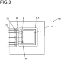
- Fig. 2 is an enlarged view of the sensor unit illustrated in Fig. 1 and Fig. 3 is a plan view of the sensor unit illustrated in Fig. 2 as viewed from above.
- the sensor chip 1 is formed of a semiconductor substrate made of silicon or the like in, for example, a rectangular parallelepiped shape with the length and the width of approximately 1 mm to 7 mm and the thickness of 30 to 400 ⁇ m.
- the sensor chip 1 has the strain detector 2 located on its principal surface 1a and electrode pads 29 located near the strain detector 2 and connected to the strain detector 2.
- the strain detector 2 is, for example, a Wheatstone bridge circuit formed of resistive elements (not shown in the drawings) formed by doping a surface of the silicon substrate with impurity ions. Accordingly, strain is detected as expansion and contraction of the sensor chip 1 in its plane direction cause changes in a resistance value of impurity diffusion resistance. If a temperature detector is formed at the sensor chip 1, temperature correction of a measured value can be made possible and strain quantity can be measured with higher accuracy. A heat strain influence on the sensor chip 1 can be reduced by outputting the detected strain as a potential difference between X-direction strain and Y-direction strain.
- Such a sensor chip is disclosed in International Publication WO2013/078183 described as PTL 1.
- a metalized layer 9 is formed over almost an entire back surface 1b of the sensor chip 1.
- the stem 4 is a rectangular-shaped thin plate member on which a seat 6 that is protruded from a central part of an upper surface 4a is formed.
- the seat 6 has a rectangular shape slightly larger than the sensor chip 1.
- a metalized layer 5 is formed on an entire upper surface of the seat 6.
- the stem 4 is made of a metallic material such as SUS, 42 alloy, invar, molybdenum, Al, Al alloy, Cu, Cu alloy, and/or CIC.
- the stem 4 can be made of materials other than metals, for example, an insulating material such as ceramics.
- the metalized layers 5 and 9 are formed by, for example, vapor deposition, sputtering, or plating and is composed of, for example, Au, Ni, Cu, Zn, Pt, Ag, Ti, Cr, or W Alternatively, the metalized layer 5 or 9 may be configured by combining two or more of the above-mentioned metals. For example, the metalized layer 5 or 9 may be configured by applying a thin Au layer over a Ni layer.
- the stem 4 may be a thin plate member of a disc shape instead of the rectangular shape.
- the stem 4 and the container 50 may be fixed together by screw fastening.
- a method of providing a male screw part on a peripheral portion 4b of the stem 4, providing a female screw part on an inner peripheral surface of the opening 56 in the container 50, and fixing the stem 4 to the container 50 by screwing the stem 4 into the container 50 and making them engage with each other can be employed as the screw fastening.
- the bonding part 3 is provided between the metalized layer 5 and the metalized layer 9 and the sensor chip 1 is bonded to the stem 4 via the bonding part 3.
- the bonding part 3 is composed of, for example, metallic materials of relatively low melting points, resin materials, and glass-based fixing materials.
- the metallic materials may include solder containing Sn as its principal component (for example, Sn-3.5 wt% Ag solder, Sn-3 wt% Ag-0.5 wt% Cu solder, Sn- 5 wt% Sb solder, and solder containing other elements such as Bi, In, and/or Zn added to the above-listed elements), Au-based solder containing a large amount of Au (for example, Au-20 wt% Sn solder, Au-12 wt% Ge solder, Au-3.15 wt% Si solder, and solder containing a third element in addition to the above-listed elements), or solder containing a large amount of Ag.
- solder containing Sn as its principal component for example, Sn-3.5 wt% Ag solder, Sn-3 wt% Ag-0.5 wt% Cu solder, Sn- 5 wt% Sb solder, and solder containing other elements such as Bi, In, and/or Zn added to the above-listed elements
- an upper surface of the bonding part 3 is bonded to almost the entire surface of the metalized layer 9.
- the upper surface of the bonding part 3 is formed so as to correspond to each side of the metalized layer 9 so that each side of the bonding part 3 substantially matches each side of the metalized layer 9.
- a lower surface of the bonding part 3 is bonded to almost the entire surface of the metalized layer 5. Since a planar size of the seat 6 at the stem 4 is slightly larger than that of the sensor chip 1, a section of the bonding part 3 has a substantially trapezoidal shape.
- the printed circuit board 20 is mounted on the upper surface 4a of the peripheral portion 4b outside the seat 6 of the stem 4. Electrode pads 21 on the printed circuit board 20 and the electrode pads 29 on the sensor chip 1 are connected via a plurality of bonding wires (lead-out wiring part) 22 using, for example, Au wires.
- the printed circuit board 20 may be a substrate using a glass epoxy material, a flexible substrate using a polyimide material or other materials, or a ceramic substrate.
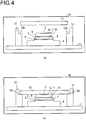
- Fig. 4(a) and Fig. 4(b) are diagrams for explaining an embodiment of a method for manufacturing the mechanical quantity measuring device illustrated in Fig. 1 .
- the metalized layer 9 is formed on the back surface 1b of the sensor chip 1 and the metalized layer 5 is formed on the upper surface of the seat 6 for the stem 4 in advance.
- the stem 4 with the metalized layer 5 formed on the upper surface of the seat 6 is placed in a heating furnace 10. Bonding correction jigs 12 for adjusting the thickness of the bonding part 3 are also set in the heating furnace 10 as described later.
- a bonding material 8 is placed on the metalized layer 5.
- This bonding material 8 is a material for the bonding part 3.
- the sensor chip 1 with the metalized layer 9 formed on the back surface 1b is mounted on the bonding material 8.
- the center of the sensor chip 1 is positioned to substantially coincide with the center of the seat 6 and the sensor chip 1 is positioned so that gaps between the respective sides of the sensor chip 1 and the respective sides of the seat 6 become almost the same. This state is illustrated in Fig. 4(a) .
- a weight 13 is mounted on the principal surface 1a of the sensor chip 1.
- Each bonding correction jig 12 is provided with a stepped part 12a on its inside surface and the weight 13 is formed with a length enabling it to be mounted on the stepped parts 12a.
- Heating is performed in this state by using, for example, a heater 11.
- the bonding material 8 melts or softens and is bonded to the metalized layer 9 on the back surface 1b of the sensor chip 1 and to the metalized layer 5 of the stem 4. Accordingly, the bonding material 8 becomes the bonding part 3.
- the thickness of the bonding part 3 can be set to a specified thickness according to the weight of the weight 13 and the shape of the bonding material 8; however, it is preferable that the thickness of the bonding part 3 should be made uniform according to the height of the stepped parts 12a of the bonding correction jigs 12 as illustrated in Fig. 4(a) and Fig. 4(b) .
- the weight of the weight 13 should be sufficiently heavy and the stepped parts 12a are designed to stop descent of the weight 13.
- the thickness of the bonding part 3 can be made uniform. This state is illustrated in Fig. 4(b) .
- N 2 is effective as the atmosphere.
- reductive hydrogen, a mixture of these elements, or organic acids such as formic acid may be used.
- organic substances such as flux capable of reducing a surface oxide may be used.
- reducing voids is effective by creating a vacuum in the heating furnace. A good bonding part 3 with little defects such as the voids can be obtained by employing such contrivance.
- the bonding material 8 is supplied onto the metalized layer 5 of the stem 4 by using the die bonder. Meanwhile, the sensor chip 1 is vacuum-sucked by using a collet or the like to press and attach the sensor chip 1 to the bonding material 8 via the metalized layer 9.
- the collet is heated with a pulse current (pulse heating) or heated with a constant current (constant heating) in the above-described state to cause the bonding material 8 to melt or soften, thereby bonding the sensor chip 1 and the stem 4 together.
- bonding time can be further shortened.
- By creating an inert atmosphere in the vicinity of the bonding part in the case of bonding by the die bonder better bonding can be achieved.
- the sensor chip 1 is substantially parallel to the upper surface of the seat 6, and the length between each side of the sensor chip 1 and each side of the seat 6 is made substantially uniform, the deformation amount transmitted through the bonding part 3 to the sensor chip 1 becomes uniform in each direction, thereby enhancing detection accuracy.
- the bonding part 3 can be easily arranged to a specified shape. In other words, if each side part of the seat 6 is located at a position too far from the range in which the molten bonding material 8 flows, there will be no advantageous effect of controlling the shape of the bonding material 8 while heated and each side of the formed bonding part 3 may easily become non-uniform.
- the detection accuracy can be enhanced by setting the length between each side of the bonding part 3 and each side of the seat 6 so that the molten bonding material 8 will substantially reach each side of the seat 6.
- each side of the bonding part 3 is formed to reach each side of the metalized layer 5, that is, each side of the seat 6 in this embodiment as described above, the detection accuracy can be enhanced.
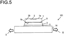
- Fig. 5 is a sectional view of a sensor unit of a comparative example.
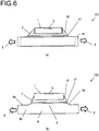
- Fig. 6(a) is a diagram illustrating deformations when a stem is displaced in the sensor unit illustrated in Fig. 5 .
- Fig. 6(b) is a diagram illustrating deformations when the stem is displaced in the sensor unit according to an embodiment of the present invention as illustrated in Fig. 2 .
- the seat 6 is not formed on a stem 14.
- the sensor unit 101 deforms from a state indicated with dotted lines in Fig. 6(a) to a state indicated with solid lines.
- the sensor chip 1 which is formed of a semiconductor substrate of silicon or the like has a large Young's modulus, it deforms less than surrounding materials. Accordingly, the bonding part 3 deforms corresponding to displacement occurring at the stem 14 and particularly large stress occurs at the side end 17 of a fillet part 16 of the bonding part 3. This stress causes creep deformation at the bonding part 3 and degrades stability of strain detection.
- the protruded seat 6 is formed on the stem 4 to increase the thickness and the rigidity of the seat 6 is higher than the rigidity of the peripheral portion 4b.
- the deformation amount of the bonding part 3 becomes smaller than the deformation amount which has occurred to the main body of the stem 4 because of the protrusion seat 6 and the stress on the side end 17 of the fillet part 16 of the bonding part 3 reduces as compared to the case where there is no protruded seat 6.
- Fig. 7 is a characteristic chart illustrating the relationship between the height of the seat on the stem and stress on the bonding part and between the height of the seat and strain on a chip surface.
- Each characteristic chart represents a change rate indicative of a rate of a value relative to a measured value when there is no seat, with respect to the height of the seat up to 300 ⁇ m.
- the stress on the bonding part is represented by a value of stress occurring at the side end 17 of the fillet part 16 of the bonding part 3.
- the seat 6 can reduce the stress occurring at the bonding part 3 and also reduce the creep deformation of the bonding part 3 and has the advantageous effect of enhancing sensor characteristics. Furthermore, the seat 6 can reduce the progress of cracks which may occur in the bonding part and is effective in enhancing the life of a sensor product.
- the mechanical quantity measuring device is designed to have the structure capable of securing the performance and satisfying sensor output stability and reliability as the mechanical quantity measuring device by setting the height of the seat 6 within the range enabling good sensitivity for measurement of the strain quantity and sufficient reduction of the stress on the bonding part.
- a two-dot chain line is an extension of the above-described characteristic curve.
- the change rate in the strain on the chip surface becomes 0 and the detection capability will be lost.
- a problem might occur upon practical use of the strain sensor when the change rate becomes less than 0.5.
- the change rate of the strain on the chip surface is equal to or more than 0.5, it can be considered to be usable as the strain sensor.
- the change rate of the strain on the chip surface is 0.5
- the corresponding height of the seat 6 is approximately 350 ⁇ m to 400 ⁇ m as indicated with a dotted line in Fig. 7 . Therefore, when the height of the seat 6 is equal to or less than 300 ⁇ m, the change rate of the strain on the chip surface is 0.5 or more so that it can be used as the strain sensor.
- the seat 6 is shaped so that its area is approximately equal to or less than ten times as large as the area of the chip; however, the seat 6 should preferably be shaped so that its area be approximately five times or less as large as the area of the chip.
- the seat 6 whose area is equal to or greater than ten times as large as that of the chip has a lower effect of reducing the stress on the bonding part 3 of the sensor chip 1.
- the seat 6 is bilaterally symmetric, or preferably symmetric with respect to a point, such as a square, a rectangle, a hexagon, or a circle as viewed from above. Also, as it is obvious from the above explanation, it is desirable that the sensor chip 1 on the protruded seat 6 should be positioned at substantially the center of the seat 6. In consideration of viewpoints such as easiness in manufacturing, cost, yield, and variability from among evaluation results of protruded seats of the above-mentioned various shapes, a square seat whose area is approximately 1.5 times as large as the area of the sensor chip and which is a protrusion seat with the height of the seat being 50 ⁇ m to 150 ⁇ m exhibits good sensor characteristics.
- Fig. 8 is a sectional view of a mechanical quantity measuring device, illustrating a variation of Embodiment 1.
- the mechanical quantity measuring device 200 has the structure in which the sensor unit 100 is fixed to the container 50.
- a mechanical quantity measuring device 201 has a structure in which the sensor unit 100 is fixed to a base (fixing part) 50A which is a measured object to be measured.
- the sensor unit 100 is the same sensor unit as the one which is used in Embodiment 1 and includes the stem 4 having the protruded seat 6, and the bonding part 3 for bonding the sensor chip 1 and the stem 4 together.
- the base 50A is a flat plate-like member without any opening and covers the entire lower surface of the stem 4.
- the metallic bonding or the mechanical bonding as mentioned in Embodiment 1 can be applied to fix the stem 4 and the base 50A together.
- the stem 4 and the base 50A can be fixed at the peripheral portion of the stem 4 or, alternatively, they can be fixed together at a central portion of the lower surface of the stem 4 or over the entire lower surface of the stem 4.
- the mechanical quantity measuring device 201 of Variation 1 detects the difference between X-direction strain and Y-direction strain which occur at the strain detector 2 of the sensor chip 1 along with deformations of the base 50A in the X-direction and the Y-direction.
- the base 50A may be simply a fixing member for fixing the stem 4 and the measured object may be attached to the base 50A. Furthermore, the base 50A which serves simply as the fixing member for fixing the stem 4 may be fixed to the peripheral portion of the opening 56 in the container 50 as illustrated in Fig. 1 to measure the pressure of the gas G in the internal space 51 of the container 50.
- Variation 1 Other structures in Variation 1 are similar to those in Embodiment 1 and the same reference numerals are assigned to corresponding members and an explanation about them has been omitted.
- Embodiment 2 of the present invention will be explained with reference to Fig. 9 to Fig. 11 .
- Fig. 9 is a sectional view illustrating Embodiment 2 of a mechanical quantity measuring device according to the present invention.
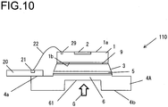
- Fig. 10 is an enlarged view of a sensor unit of the mechanical quantity measuring device illustrated in Fig. 9 .
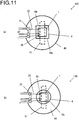
- Fig. 11(a) and Fig. 11(b) are respectively plan views of the sensor unit illustrated in Fig. 10 as viewed from above.
- Fig. 11(a) is an example where a planar shape of the base 6 is a rectangular shape
- Fig. 11(b) is an example where the planar shape of the base 6 is a circular shape.
- a stem 4A is configured as a disc-shaped thin plate member.
- the difference between the mechanical quantity measuring device 201 of Embodiment 2 and the mechanical quantity measuring device in Embodiment 1 is that a groove 61 is formed in the stem 4A of the sensor unit 110.
- Embodiment 2 will be explained below by focusing on this difference.
- the rectangular groove 61 is formed on a surface of the stem 4A, that is the other surface of the side on which the seat 6 is formed, namely, on the side facing the internal space 51 of the container 50.
- the length of a short side of the rectangular groove 61 is formed to be narrower than the width of the seat 6.
- the groove 61 is formed in an oblong rectangular shape extending from outside of one side end 19a to outside of the other opposite side end 19b across a substantially central part of the seat 6 at the stem 4A as illustrated in Fig. 11(a) . Both ends of the groove 61 extending across the back surface of the stem 4A do not continuously extend beyond the peripheral portion of the stem 4A towards outside, so that specified rigidity is thereby retained.
- a pair of side edges along the lengthwise direction of the groove 61 extends in parallel with a pair of sides of the sensor chip 1. Furthermore, the depth of the groove 61 is designed so that the bottom of the groove 61 does not reach the upper surface 4a of the stem 4A.
- the seat 6 becomes partially thin and the stem 4A is configured as a diaphragm with low rigidity.
- the pressure of the gas G is applied to inside of the container 50 for such mechanical quantity measuring device 201
- the thin thickness part of the seat 6 which serves as the diaphragm deforms preferentially.
- the strain detector 2 of the sensor chip 1 measures the strain, that is, the pressure.
- a pressure sensor for measuring the pressure inside piping can be configured by making the container 50 serve as, for example, a pressure measuring part which branches off from piping where a fluid to be measured flows.
- the groove 61 which is parallel to the pair of side edges of the sensor chip 1 is formed at the seat 6 of the stem 4A. Since the thin thickness part of the seat 6 for the stem 4A has low rigidity, that part easily deforms.
- the groove 61 is formed in a rectangular shape, the strain on the sensor chip 1 as caused by the deformation of the stem 4A is larger in a direction perpendicular to the lengthwise direction than in the lengthwise direction and the detection capability of the sensor chip 1 which outputs the strain difference can be enhanced.
- the sensor unit 110 described in Embodiment 2 also has the same advantageous effects as those of Embodiment 1.
- the planar shape of the seat 6 may be a rectangular shape as illustrated in Fig. 11(a) , but may also be a circular shape as illustrated in Fig. 11(b) . If the seat 6 is formed in the circular shape as illustrated in Fig. 11(b) , the seat 6 can be formed easily and the efficiency of processing steps can be enhanced. Incidentally, even when the seat 6 is circular as illustrated in Fig. 11(b) , the groove 61 is provided through the center of the seat 6 and extends across an outer periphery 19c of the seat 6.
- Embodiment 2 has the same advantageous effects as those of Embodiment 1.
- Embodiment 2 Other structures in Embodiment 2 are similar to those in Embodiment 1 and the same reference numerals are assigned to corresponding members and an explanation about them has been omitted.
- Fig. 12 and Fig. 13 illustrate a sensor unit of a mechanical quantity measuring device according to Embodiment 3 of the present invention.
- Fig. 12 is a sectional view of the sensor unit according to Embodiment 3 and Fig. 13(a) and Fig. 13(b) are respectively plan views of the sensor unit illustrated in Fig. 12 as viewed from above.
- Fig. 13(a) is an example where the planar shape of the seat 6 is a rectangular shape
- Fig. 13(b) is an example where the planar shape of the seat 6 is a circular shape.
- a stem 4B is configured as a disc-shaped thin plate member.
- a sensor unit 120 of Embodiment 3 The difference between a sensor unit 120 of Embodiment 3 and the sensor unit 110 of Embodiment 2 is that the upper surface 4a of the stem 4B is flat and a seat 6A is defined by a frame-like groove part 62 formed in a central part of the sensor unit 120.
- the frame-like groove part 62 is provided in the upper surface 4a of the stem 4B and the seat 6A is formed inside this frame-like groove part 62.
- the upper surface of the seat 6A is flush with the upper surface 4a of the peripheral portion 4b and is flush with the surface on which the printed circuit board 20 is mounted.
- the planar shape of the groove part 62 may be a rectangular shape as illustrated in Fig. 13(a) , or may be a circular shape as illustrated in Fig. 13(b) . If the seat 6A is formed in the circular shape as illustrated in Fig. 13(b) , the seat 6 can be formed easily and the efficiency of processing steps can be enhanced.
- the shape of the groove part 62 illustrated in Fig. 13(a) is a square shape, but it may be an oblong rectangular shape.
- the seat 6A is formed by forming the groove 62 by means of, for example, counter boring or laser processing. Therefore, the efficiency of the processing steps can be enhanced better than Embodiment 2 in which the protruded base 6 is formed.
- the groove part 62 in the stem 4 may be formed before it is bonded to the sensor chip 1 or after it is bonded to the sensor chip 1.
- the groove part 62 can be formed advantageously before bonded to the sensor chip 1 so that problems such as grinding sludge generated at the time of processing or contamination of the sensor chip will not be caused.
- the groove part 62 is formed after it is bonded to the sensor chip 1, there is an advantage of no flowing of the bonding material 8 into the groove 61.
- the groove part 62 can be formed by, for example, shifting the center of the groove part 62 to coincide with the center position of the fillet part 16 or the center position of the sensor chip 1 so that modifications can be made.
- the sensor unit 120 described in Embodiment 3 also has the same advantageous effects as those of the sensor unit 110 in Embodiment 2.
- Embodiment 3 has the same advantageous effects as those of Embodiment 2.
- Embodiment 3 Other structures in Embodiment 3 are similar to those in Embodiment 1 and the same reference numerals are assigned to corresponding members and an explanation about them has been omitted.
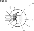
- Fig. 14 is a plan view illustrating a variation of Embodiment 3.
- a pair of groove parts 63 in parallel with the side edges of the groove 61 in its lengthwise direction is formed, in place of the frame-like groove part 62, with the length of the groove parts 63 longer than the length (width) of the sensor chip 1.
- a region inside the pair of groove parts 63 that is, a region between one groove part 63 and the other groove part 63 is flush with the upper surface 4a of the peripheral portion 4b and is formed continuously with the peripheral portion 4b. Therefore, no seat which is clearly separated from the peripheral portion 4b is formed.
- the pair of groove parts 63 is formed symmetrically with respect to the x-axis and y-axis passing through the center of the sensor chip 1.
- the groove 61 formed in the lower surface of the stem 4C is also in a shape symmetrical with respect to the x-axis and y-axis passing through the center of the sensor chip 1.
- no groove which serves as a boundary with the peripheral portion 4b is formed in the stem 4C in a direction perpendicular to the pair of groove parts 63 and a region to be the seat ((6A) in Fig. 14 ) is defined as the inside region set by the pair of groove parts 63 facing opposite each other.
- the rigidity of the thin thickness part of the stem 4C where the groove 61 is formed is low, so that the stem 4C deforms preferentially.
- the region to be the seat where the sensor chip 1 is mounted is provided inside the pair of groove parts 63. Therefore, similarly to Embodiment 3, it is possible to reduce the stress on the side end 17 of the fillet part 16, reduce the creep deformation amount of the bonding part 3 in use, and contribute to the stability of the sensor output value.
- the pair of groove parts 63 in parallel with the side edges of the groove 61 in its lengthwise direction is formed in the stem 4C; however, a pair of groove parts in parallel with the side edges of the groove 61 in its transverse direction may be formed with the length of the groove parts longer than the length (width) of the sensor chip 1.
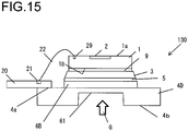
- Fig. 15 is a sectional view illustrating Embodiment 4 of a sensor unit of a mechanical quantity measuring device according to the present invention.
- a seat 6B is formed by means of film formation such as plating, vapor deposition, or sputtering.
- An upper surface 4a of a stem 4D is flat and the groove 61 is formed in its lower surface.
- the seat 6B is formed at approximately the center of the upper surface 4a of the stem 4D.
- the seat 6B should preferably be formed by means of plating, but may be formed by means of vapor deposition or sputtering as mentioned above. In a case of plating, Ni, Cu, and so on can be used.
- the Young's modulus of Cu is approximately 110 GPa, which is larger than approximately 57 GPa, that is, the Young's modulus of Au- 20 wt% Sn solder which is considered to be a rigid material among solders.
- a thin thickness part of the stem 4D where the groove 61 is formed deforms preferentially. This deformation is transmitted to the sensor chip 1 bonded to the seat 6B via the bonding part 3. As a result, the strain detector 2 of the sensor chip 1 measures strain, that is, the pressure.
- the sensor unit 130 indicated in Embodiment 4 also has the same advantageous effects as those of Embodiment 2.
- the metalized layers 5 and 9 formed on the seat 6, 6A, or 6B and the sensor chip 1 are not necessarily requisite and either one or both of them may not be formed.
- the printed circuit board 20 does not have to be located on the upper surface 4a of the stem 4, 4B, 4C, or 4D.
- a mechanical quantity measuring device may be obtained by combining the aforementioned respective embodiments and the variations with each other.
- the sensor unit 110, 120, or 130 described in Embodiment 2 to 4 can be solely used as a mechanical quantity measuring device without being secured to, for example, the container 50.
- the present invention can also be adapted to any structures in which the structures described in the respective embodiments are appropriately modified.
- the mechanical quantity measuring device equipped with the sensor unit bonded to the upper surface of the seat formed on the stem via the bonding material formed of the metallic material or the glass material it is only required that the stem and the fixing part should be integrally molded or fixed through metallic bonding or mechanical bonding.
Landscapes
- Physics & Mathematics (AREA)
- General Physics & Mathematics (AREA)
- Chemical & Material Sciences (AREA)
- Analytical Chemistry (AREA)
- Measuring Fluid Pressure (AREA)
- Pressure Sensors (AREA)
Abstract
Description
- The present invention relates to a mechanical quantity measuring device equipped with a strain detector and to a sensor unit.
- A technique that employs a metal foil strain gauge which utilizes changes in a resistance value of a metal foil as caused by strain is known as a method for measuring deformations such as strain on a measurement object. This is a technique that enables measurement of strain on the measurement object by adhesively attaching the strain gauge to the measurement object, causing the metal foil to change its length in accordance with the strain on the measurement object, and detecting changes in the resistance value of the metal foil as a result of changing its length.
- A semiconductor strain sensor in which a semiconductor piezoelectric element is formed by doping a surface of a semiconductor substrate with impurities is being examined as a mechanical quantity measuring device for measuring the deformations such as the strain on the measurement object with high accuracy.
- One example of such semiconductor strain sensor is known which has a structure in which a sensor chip equipped with a semiconductor strain unit is soldered onto a metallic stem and the metallic stem is adhesively attached to the measurement object by using an adhesive agent made of resin.
- It is described that the metallic stem interposed between the measured object and the sensor chip reduces the strain caused on the sensor chip due to the deformations of the measurement object and prevents or inhibits breakage of the sensor chip (see PTL 1).
- PTL 1: International Publication
WO2013/078183 - When the mechanical quantity measuring device described in the above-mentioned
PTL 1 is used under a high-temperature environment, the adhesive agent made of resin for adhesively attaching the measurement object and the metallic stem together deteriorates or is modified, thereby resulting in insufficient bonding power. Accordingly, the deformations of the measurement object will not accurately impose the load on the metallic stem and detection accuracy will degrade. - A mechanical quantity measuring device according to a first aspect of the present invention comprises: a sensor chip having a strain detector formed on a surface of a semiconductor substrate and a plurality of electrodes connected to the strain detector; a stem having a seat that protrudes from an adjacent peripheral portion and has an upper surface that is attached to a lower surface of the sensor chip by a bonding material formed from a metallic material or a glass material; a lead-out wiring part including a plurality of wires that are electrically connected to the plurality of electrodes; and a fixing part for fixing the stem, wherein: the stem and the fixing part are integrally molded or fixed through metallic bonding or mechanical bonding.
- According to the present invention, the load generated on the fixing part is transmitted to the stem almost without any loss. Therefore, high-accuracy detection capability can be maintained even under the high-temperature environment.
-
- [
Fig. 1] Fig. 1 is a sectional view of an embodiment of a mechanical quantity measuring device according to the present invention; - [
Fig. 2] Fig. 2 is an enlarged view of a sensor unit illustrated inFig. 1 ; - [
Fig. 3] Fig. 3 is a plan view of the sensor unit illustrated inFig. 2 as viewed from above; - [
Fig. 4] Fig. 4(a) and Fig. 4(b) are diagrams for explaining an embodiment of a method for manufacturing the mechanical quantity measuring device illustrated inFig. 1 ; - [
Fig. 5] Fig. 5 is a sectional view of a sensor unit of a comparative example; - [
Fig. 6] Fig. 6(a) is a diagram illustrating deformations when a stem is displaced in the sensor unit illustrated inFig. 5 ; andFig. 6(b) is a diagram illustrating deformations when the stem is displaced in the sensor unit according to the present invention as illustrated inFig. 2 ; - [
Fig. 7] Fig. 7 is a characteristic chart illustrating the relationship between the height of a seat on the stem and stress on a bonding part and between the height of the seat and strain on a chip surface; - [
Fig. 8] Fig. 8 is a sectional view of a mechanical quantity measuring device, illustrating a variation ofEmbodiment 1; - [
Fig. 9] Fig. 9 is a sectionalview illustrating Embodiment 2 of a mechanical quantity measuring device according to the present invention; - [
Fig. 10]Fig. 10 is an enlarged view of a sensor unit of the mechanical quantity measuring device illustrated inFig. 9 ; - [
Fig. 11] Fig. 11(a) and Fig. 11(b) are respectively plan views of the sensor unit illustrated inFig. 10 as viewed from above; - [
Fig. 12]Fig. 12 is a sectionalview illustrating Embodiment 3 of a sensor unit of a mechanical quantity measuring device according to the present invention; - [
Fig. 13]Fig. 13(a) and Fig. 13(b) are respectively plan views of the sensor unit illustrated inFig. 12 as viewed from above; - [
Fig. 14]Fig. 14 is a plan view illustrating a variation ofEmbodiment 3; and - [
Fig. 15]Fig. 15 is a sectionalview illustrating Embodiment 4 of a sensor unit of a mechanical quantity measuring device according to the present invention. - A basic structure of a mechanical quantity measuring device according to an embodiment of the present invention is as follows.
- A sensor chip has a strain detector formed on a surface of a semiconductor substrate and a plurality of electrodes connected to the strain detector. A stem has a seat that protrudes from an adjacent peripheral portion. An upper surface of the seat at the stem is bonded to a lower surface of the sensor chip by a bonding material formed from a metallic material or a glass material. The mechanical quantity measuring device further includes a fixing part for fixing the stem. The stem and the fixing part are integrally molded or fixed through welding or mechanical bonding and do not have a fixing structure that uses an adhesive agent made of resin.
- The mechanical quantity measuring device according to an embodiment of the present invention can adopt an aspect in which the fixing part is a measured object.
- Moreover, the mechanical quantity measuring device according to an embodiment of the present invention can adopt an aspect in which an opening is formed at the fixing part so as to expose the stem and pressures of gas and liquid that act on the stem via the opening are measured. This aspect should preferably employ a structure to provide a groove to partly reduce rigidity of the stem on a back surface of the seat at the stem.
- Embodiments with respect to the above-described respective aspects will be explained below with reference to drawings.
- An embodiment of the mechanical quantity measuring device according to the present invention will be explained with reference to
Fig. 1 to Fig. 3 . -
Fig. 1 is a sectional view of the embodiment of the mechanical quantity measuring device according to the present invention. - A mechanical
quantity measuring device 200 is composed of asensor unit 100, a container (fixing part) 50 into which gas G to be measured is introduced, and acase 58. - The
sensor unit 100 includes asensor chip 1, astem 4, a printedcircuit board 20,bonding wires 22 for connecting electrodes of thesensor chip 1 and connecting terminals of the printedcircuit board 20, and abonding part 3 for bonding thesensor chip 1 and thestem 4. - The
sensor chip 1 has a strain detector 2 (seeFig. 2 ) as described later and the mechanicalquantity measuring device 200 detects the pressure of the gas G which flows into aninternal space 51 of thecontainer 50. - The
container 50 is made from, for example, SUS and is formed in a cylindrical shape and thestem 4 of thesensor unit 100 is fixed to thecontainer 50. Thecase 58 is formed of a resin or metallic member and protects thesensor unit 100 fixed to thecontainer 50. - The
container 50 is formed in a hollow, substantially cylindrical shape having theinternal space 51. Agas intake 54 that introduces the gas G into theinternal container 51 is formed in a lower part of thecontainer 50 and anopening 56 that exposes the lower surface of thestem 4 is formed in an upper part of thecontainer 50. In other words, thecontainer 50 is formed as a cylindrical pressure introducing part. - The
stem 4 is made from, for example, Fe-Ni alloys (such as 42 alloy or invar), Mo, SUS, or Al. Thestem 4 also functions as a cover of thecontainer 50. - The
stem 4 and thecontainer 50 are integrally molded or fixed through metallic bonding or mechanical bonding such as fastening or crimping. Specifically speaking, the mechanicalquantity measuring device 200 fixes the stem to a fixing part, that is, thecontainer 50 by a highly heat-resistant fixing method. Examples of a method of the integral molding or integral forming include sheet metal working such as drawing. Regarding the metallic bonding, laser welding, ultrasonic welding, friction stir welding, soldering, or brazing can be applied. Regarding the fastening, for example, it is possible to employ a method of inserting a fastening member such as a screw into an opening (not shown) in thestem 4 and fastening it to a female screw part (not shown) of thecontainer 50. Regarding the crimping, for example, it is possible to use a structure to fix the peripheral portion of thestem 4 by means of a crimping member provided at theopening 56 in thecontainer 50. -
Fig. 2 is an enlarged view of the sensor unit illustrated inFig. 1 andFig. 3 is a plan view of the sensor unit illustrated inFig. 2 as viewed from above. - The
sensor chip 1 is formed of a semiconductor substrate made of silicon or the like in, for example, a rectangular parallelepiped shape with the length and the width of approximately 1 mm to 7 mm and the thickness of 30 to 400µm. Thesensor chip 1 has thestrain detector 2 located on itsprincipal surface 1a andelectrode pads 29 located near thestrain detector 2 and connected to thestrain detector 2. - The
strain detector 2 is, for example, a Wheatstone bridge circuit formed of resistive elements (not shown in the drawings) formed by doping a surface of the silicon substrate with impurity ions. Accordingly, strain is detected as expansion and contraction of thesensor chip 1 in its plane direction cause changes in a resistance value of impurity diffusion resistance. If a temperature detector is formed at thesensor chip 1, temperature correction of a measured value can be made possible and strain quantity can be measured with higher accuracy. A heat strain influence on thesensor chip 1 can be reduced by outputting the detected strain as a potential difference between X-direction strain and Y-direction strain. - Such a sensor chip is disclosed in International Publication
WO2013/078183 described asPTL 1. - A metalized
layer 9 is formed over almost anentire back surface 1b of thesensor chip 1. - The
stem 4 is a rectangular-shaped thin plate member on which aseat 6 that is protruded from a central part of anupper surface 4a is formed. Theseat 6 has a rectangular shape slightly larger than thesensor chip 1. A metalizedlayer 5 is formed on an entire upper surface of theseat 6. Thestem 4 is made of a metallic material such as SUS, 42 alloy, invar, molybdenum, Al, Al alloy, Cu, Cu alloy, and/or CIC. Thestem 4 can be made of materials other than metals, for example, an insulating material such as ceramics. - The metalized layers 5 and 9 are formed by, for example, vapor deposition, sputtering, or plating and is composed of, for example, Au, Ni, Cu, Zn, Pt, Ag, Ti, Cr, or W Alternatively, the metalized
layer layer - Incidentally, the
stem 4 may be a thin plate member of a disc shape instead of the rectangular shape. In this case, thestem 4 and thecontainer 50 may be fixed together by screw fastening. For example, a method of providing a male screw part on aperipheral portion 4b of thestem 4, providing a female screw part on an inner peripheral surface of theopening 56 in thecontainer 50, and fixing thestem 4 to thecontainer 50 by screwing thestem 4 into thecontainer 50 and making them engage with each other can be employed as the screw fastening. - The
bonding part 3 is provided between the metalizedlayer 5 and the metalizedlayer 9 and thesensor chip 1 is bonded to thestem 4 via thebonding part 3. Thebonding part 3 is composed of, for example, metallic materials of relatively low melting points, resin materials, and glass-based fixing materials. Examples of the metallic materials may include solder containing Sn as its principal component (for example, Sn-3.5 wt% Ag solder, Sn-3 wt% Ag-0.5 wt% Cu solder, Sn- 5 wt% Sb solder, and solder containing other elements such as Bi, In, and/or Zn added to the above-listed elements), Au-based solder containing a large amount of Au (for example, Au-20 wt% Sn solder, Au-12 wt% Ge solder, Au-3.15 wt% Si solder, and solder containing a third element in addition to the above-listed elements), or solder containing a large amount of Ag. - An upper surface of the
bonding part 3 is bonded to almost the entire surface of the metalizedlayer 9. Specifically speaking, the upper surface of thebonding part 3 is formed so as to correspond to each side of the metalizedlayer 9 so that each side of thebonding part 3 substantially matches each side of the metalizedlayer 9. Similarly, a lower surface of thebonding part 3 is bonded to almost the entire surface of the metalizedlayer 5. Since a planar size of theseat 6 at thestem 4 is slightly larger than that of thesensor chip 1, a section of thebonding part 3 has a substantially trapezoidal shape. - At least part of the printed
circuit board 20 is mounted on theupper surface 4a of theperipheral portion 4b outside theseat 6 of thestem 4.Electrode pads 21 on the printedcircuit board 20 and theelectrode pads 29 on thesensor chip 1 are connected via a plurality of bonding wires (lead-out wiring part) 22 using, for example, Au wires. The printedcircuit board 20 may be a substrate using a glass epoxy material, a flexible substrate using a polyimide material or other materials, or a ceramic substrate. - An embodiment of a method for bonding the
sensor chip 1 and thestem 4 will be explained. -
Fig. 4(a) and Fig. 4(b) are diagrams for explaining an embodiment of a method for manufacturing the mechanical quantity measuring device illustrated inFig. 1 . - The metalized
layer 9 is formed on theback surface 1b of thesensor chip 1 and the metalizedlayer 5 is formed on the upper surface of theseat 6 for thestem 4 in advance. - The
stem 4 with the metalizedlayer 5 formed on the upper surface of theseat 6 is placed in aheating furnace 10. Bonding correction jigs 12 for adjusting the thickness of thebonding part 3 are also set in theheating furnace 10 as described later. - A
bonding material 8 is placed on the metalizedlayer 5. Thisbonding material 8 is a material for thebonding part 3. Thesensor chip 1 with the metalizedlayer 9 formed on theback surface 1b is mounted on thebonding material 8. The center of thesensor chip 1 is positioned to substantially coincide with the center of theseat 6 and thesensor chip 1 is positioned so that gaps between the respective sides of thesensor chip 1 and the respective sides of theseat 6 become almost the same. This state is illustrated inFig. 4(a) . - A
weight 13 is mounted on theprincipal surface 1a of thesensor chip 1. Eachbonding correction jig 12 is provided with a steppedpart 12a on its inside surface and theweight 13 is formed with a length enabling it to be mounted on the steppedparts 12a. - Heating is performed in this state by using, for example, a
heater 11. When the temperature of thestem 4 rises as a result of heating, thebonding material 8 melts or softens and is bonded to the metalizedlayer 9 on theback surface 1b of thesensor chip 1 and to the metalizedlayer 5 of thestem 4. Accordingly, thebonding material 8 becomes thebonding part 3. - The thickness of the
bonding part 3 can be set to a specified thickness according to the weight of theweight 13 and the shape of thebonding material 8; however, it is preferable that the thickness of thebonding part 3 should be made uniform according to the height of the steppedparts 12a of the bonding correction jigs 12 as illustrated inFig. 4(a) and Fig. 4(b) . In this case, the weight of theweight 13 should be sufficiently heavy and the steppedparts 12a are designed to stop descent of theweight 13. As a result, the thickness of thebonding part 3 can be made uniform. This state is illustrated inFig. 4(b) . - Under this circumstance, it is possible to prevent oxidation of the surface of the
bonding material 8 and achieve good bonding by controlling the atmosphere inside theheating furnace 10. For example, N2 is effective as the atmosphere. Besides this, reductive hydrogen, a mixture of these elements, or organic acids such as formic acid may be used. Moreover, organic substances such as flux capable of reducing a surface oxide may be used. Furthermore, reducing voids is effective by creating a vacuum in the heating furnace. Agood bonding part 3 with little defects such as the voids can be obtained by employing such contrivance. In order to further enhance bondability, it is effective to apply, for example, sputtering processing or plasma cleaning to thestem 4, theback surface 1b of thesensor chip 1, the surface of thebonding material 8, and so on before bonding them so as to remove or reduce an organic contamination amount of the bonding member or oxide films. - The above explanation was given about the method of bonding the
sensor chip 1 and thestem 4 by using theheating furnace 10. However, thesensor chip 1 and thestem 4 can be bonded by using a die bonder. - An example of the case where the die bonder is used will be explained below. The
bonding material 8 is supplied onto the metalizedlayer 5 of thestem 4 by using the die bonder. Meanwhile, thesensor chip 1 is vacuum-sucked by using a collet or the like to press and attach thesensor chip 1 to thebonding material 8 via themetalized layer 9. The collet is heated with a pulse current (pulse heating) or heated with a constant current (constant heating) in the above-described state to cause thebonding material 8 to melt or soften, thereby bonding thesensor chip 1 and thestem 4 together. By heating the base substrate in advance, bonding time can be further shortened. By creating an inert atmosphere in the vicinity of the bonding part in the case of bonding by the die bonder, better bonding can be achieved. - When the thickness of the
bonding part 3 has little variability, thesensor chip 1 is substantially parallel to the upper surface of theseat 6, and the length between each side of thesensor chip 1 and each side of theseat 6 is made substantially uniform, the deformation amount transmitted through thebonding part 3 to thesensor chip 1 becomes uniform in each direction, thereby enhancing detection accuracy. As a flow of themolten bonding material 8 is stopped by each side part of theseat 6, thebonding part 3 can be easily arranged to a specified shape. In other words, if each side part of theseat 6 is located at a position too far from the range in which themolten bonding material 8 flows, there will be no advantageous effect of controlling the shape of thebonding material 8 while heated and each side of the formedbonding part 3 may easily become non-uniform. Specifically speaking, the detection accuracy can be enhanced by setting the length between each side of thebonding part 3 and each side of theseat 6 so that themolten bonding material 8 will substantially reach each side of theseat 6. - Since each side of the
bonding part 3 is formed to reach each side of the metalizedlayer 5, that is, each side of theseat 6 in this embodiment as described above, the detection accuracy can be enhanced. - Functions of the
seat 6 for thestem 4 will be explained. -
Fig. 5 is a sectional view of a sensor unit of a comparative example.Fig. 6(a) is a diagram illustrating deformations when a stem is displaced in the sensor unit illustrated inFig. 5 .Fig. 6(b) is a diagram illustrating deformations when the stem is displaced in the sensor unit according to an embodiment of the present invention as illustrated inFig. 2 . - Regarding a
sensor unit 101 illustrated inFig. 5 , theseat 6 is not formed on astem 14. When a load is imposed on thestem 14 in X-directions indicated with arrows, thesensor unit 101 deforms from a state indicated with dotted lines inFig. 6(a) to a state indicated with solid lines. Specifically speaking, since thesensor chip 1 which is formed of a semiconductor substrate of silicon or the like has a large Young's modulus, it deforms less than surrounding materials. Accordingly, thebonding part 3 deforms corresponding to displacement occurring at thestem 14 and particularly large stress occurs at the side end 17 of afillet part 16 of thebonding part 3. This stress causes creep deformation at thebonding part 3 and degrades stability of strain detection. - On the other hand, regarding the
sensor unit 100 with theprotruded seat 6 formed on thestem 4 according to an embodiment of the present invention, theprotruded seat 6 is formed on thestem 4 to increase the thickness and the rigidity of theseat 6 is higher than the rigidity of theperipheral portion 4b. - Accordingly, when the load is imposed on the
stem 4 in the X-directions indicated with arrows as illustrated inFig. 6(b) , part of theprotruded seat 6 close to a main body of thestem 4 deforms, but a deformation amount reduces at positions further away from the main body of thestem 4. Specifically speaking, side faces 18 of theprotruded seat 6 form a shape inclined with respect to the X-directions relative to the stem 4 (the shape whose section is close to a trapezoid). Therefore, the deformation amount of thebonding part 3 becomes smaller than the deformation amount which has occurred to the main body of thestem 4 because of theprotrusion seat 6 and the stress on the side end 17 of thefillet part 16 of thebonding part 3 reduces as compared to the case where there is noprotruded seat 6. - In this way, it becomes possible to suppress the creep deformation occurring at the
bonding part 3, secure stability of the strain detection, and increase its life as a sensor by providing thestem 4 with theprotruded seat 6. -
Fig. 7 is a characteristic chart illustrating the relationship between the height of the seat on the stem and stress on the bonding part and between the height of the seat and strain on a chip surface. Each characteristic chart represents a change rate indicative of a rate of a value relative to a measured value when there is no seat, with respect to the height of the seat up to 300 µm. The stress on the bonding part is represented by a value of stress occurring at the side end 17 of thefillet part 16 of thebonding part 3. - Referring to stress characteristics of the bonding part, as the height of the
seat 6 increases, the stress occurring at the side end 17 of thefillet part 16 of thebonding part 3 decreases. Specifically speaking, theseat 6 can reduce the stress occurring at thebonding part 3 and also reduce the creep deformation of thebonding part 3 and has the advantageous effect of enhancing sensor characteristics. Furthermore, theseat 6 can reduce the progress of cracks which may occur in the bonding part and is effective in enhancing the life of a sensor product. - Referring to characteristics of the strain on the chip surface, as the height of the
protruded seat 6 increases, the strain occurring on the chip surface decreases. - As the strain quantity on the surface of the
sensor chip 1 reduces, it may be considered that sensitivity as the sensor might degrade. However, a rate of decrease in the strain quantity of thesensor chip 1 is lower than a rate of decrease in the stress on thebonding part 3. Therefore, the mechanical quantity measuring device is designed to have the structure capable of securing the performance and satisfying sensor output stability and reliability as the mechanical quantity measuring device by setting the height of theseat 6 within the range enabling good sensitivity for measurement of the strain quantity and sufficient reduction of the stress on the bonding part. - Regarding the characteristics of the strain on the chip surface in
Fig. 7 , a two-dot chain line is an extension of the above-described characteristic curve. When the height of theseat 6 is approximately 700 µm, the change rate in the strain on the chip surface becomes 0 and the detection capability will be lost. In consideration of detection accuracy of the strain sensor, a problem might occur upon practical use of the strain sensor when the change rate becomes less than 0.5. In other words, when the change rate of the strain on the chip surface is equal to or more than 0.5, it can be considered to be usable as the strain sensor. When the change rate of the strain on the chip surface is 0.5, the corresponding height of theseat 6 is approximately 350 µm to 400 µm as indicated with a dotted line inFig. 7 . Therefore, when the height of theseat 6 is equal to or less than 300 µm, the change rate of the strain on the chip surface is 0.5 or more so that it can be used as the strain sensor. - It has been found as results of such stress analysis, bondability examination, and characteristic evaluation that a certain degree of advantageous effects can be obtained when the
seat 6 is shaped so that its area is approximately equal to or less than ten times as large as the area of the chip; however, theseat 6 should preferably be shaped so that its area be approximately five times or less as large as the area of the chip. Theseat 6 whose area is equal to or greater than ten times as large as that of the chip has a lower effect of reducing the stress on thebonding part 3 of thesensor chip 1. - Furthermore, it is important that the
seat 6 is bilaterally symmetric, or preferably symmetric with respect to a point, such as a square, a rectangle, a hexagon, or a circle as viewed from above. Also, as it is obvious from the above explanation, it is desirable that thesensor chip 1 on theprotruded seat 6 should be positioned at substantially the center of theseat 6. In consideration of viewpoints such as easiness in manufacturing, cost, yield, and variability from among evaluation results of protruded seats of the above-mentioned various shapes, a square seat whose area is approximately 1.5 times as large as the area of the sensor chip and which is a protrusion seat with the height of the seat being 50 µm to 150 µm exhibits good sensor characteristics. -
Fig. 8 is a sectional view of a mechanical quantity measuring device, illustrating a variation ofEmbodiment 1. - The mechanical
quantity measuring device 200 according toEmbodiment 1 has the structure in which thesensor unit 100 is fixed to thecontainer 50. In the variation inFig. 8 , a mechanicalquantity measuring device 201 has a structure in which thesensor unit 100 is fixed to a base (fixing part) 50A which is a measured object to be measured. Thesensor unit 100 is the same sensor unit as the one which is used inEmbodiment 1 and includes thestem 4 having the protrudedseat 6, and thebonding part 3 for bonding thesensor chip 1 and thestem 4 together. - The
base 50A is a flat plate-like member without any opening and covers the entire lower surface of thestem 4. The metallic bonding or the mechanical bonding as mentioned inEmbodiment 1 can be applied to fix thestem 4 and thebase 50A together. However, thestem 4 and thebase 50A can be fixed at the peripheral portion of thestem 4 or, alternatively, they can be fixed together at a central portion of the lower surface of thestem 4 or over the entire lower surface of thestem 4. - The mechanical
quantity measuring device 201 ofVariation 1 detects the difference between X-direction strain and Y-direction strain which occur at thestrain detector 2 of thesensor chip 1 along with deformations of thebase 50A in the X-direction and the Y-direction. - Although the
base 50A is illustrated as the measured object, thebase 50A may be simply a fixing member for fixing thestem 4 and the measured object may be attached to thebase 50A. Furthermore, thebase 50A which serves simply as the fixing member for fixing thestem 4 may be fixed to the peripheral portion of theopening 56 in thecontainer 50 as illustrated inFig. 1 to measure the pressure of the gas G in theinternal space 51 of thecontainer 50. - Other structures in
Variation 1 are similar to those inEmbodiment 1 and the same reference numerals are assigned to corresponding members and an explanation about them has been omitted. -
Embodiment 2 of the present invention will be explained with reference toFig. 9 to Fig. 11 . -
Fig. 9 is a sectionalview illustrating Embodiment 2 of a mechanical quantity measuring device according to the present invention.Fig. 10 is an enlarged view of a sensor unit of the mechanical quantity measuring device illustrated inFig. 9 .Fig. 11(a) and Fig. 11(b) are respectively plan views of the sensor unit illustrated inFig. 10 as viewed from above.Fig. 11(a) is an example where a planar shape of thebase 6 is a rectangular shape andFig. 11(b) is an example where the planar shape of thebase 6 is a circular shape. Incidentally, inEmbodiment 2, astem 4A is configured as a disc-shaped thin plate member. - The difference between the mechanical
quantity measuring device 201 ofEmbodiment 2 and the mechanical quantity measuring device inEmbodiment 1 is that agroove 61 is formed in thestem 4A of thesensor unit 110. -
Embodiment 2 will be explained below by focusing on this difference. - The
rectangular groove 61 is formed on a surface of thestem 4A, that is the other surface of the side on which theseat 6 is formed, namely, on the side facing theinternal space 51 of thecontainer 50. The length of a short side of therectangular groove 61 is formed to be narrower than the width of theseat 6. Thegroove 61 is formed in an oblong rectangular shape extending from outside of oneside end 19a to outside of the otheropposite side end 19b across a substantially central part of theseat 6 at thestem 4A as illustrated inFig. 11(a) . Both ends of thegroove 61 extending across the back surface of thestem 4A do not continuously extend beyond the peripheral portion of thestem 4A towards outside, so that specified rigidity is thereby retained. A pair of side edges along the lengthwise direction of thegroove 61 extends in parallel with a pair of sides of thesensor chip 1. Furthermore, the depth of thegroove 61 is designed so that the bottom of thegroove 61 does not reach theupper surface 4a of thestem 4A. - Specifically speaking, because the
groove 61 is formed in thestem 4A, theseat 6 becomes partially thin and thestem 4A is configured as a diaphragm with low rigidity. When the pressure of the gas G is applied to inside of thecontainer 50 for such mechanicalquantity measuring device 201, the thin thickness part of theseat 6 which serves as the diaphragm deforms preferentially. This deformation is transmitted to thesensor chip 1 bonded to theseat 6 via thebonding part 3. Accordingly, thestrain detector 2 of thesensor chip 1 measures the strain, that is, the pressure. A pressure sensor for measuring the pressure inside piping can be configured by making thecontainer 50 serve as, for example, a pressure measuring part which branches off from piping where a fluid to be measured flows. - In
Embodiment 2, thegroove 61 which is parallel to the pair of side edges of thesensor chip 1 is formed at theseat 6 of thestem 4A. Since the thin thickness part of theseat 6 for thestem 4A has low rigidity, that part easily deforms. - Since the
groove 61 is formed in a rectangular shape, the strain on thesensor chip 1 as caused by the deformation of thestem 4A is larger in a direction perpendicular to the lengthwise direction than in the lengthwise direction and the detection capability of thesensor chip 1 which outputs the strain difference can be enhanced. - If a structure in which the
stem 4A had no protrudedseat 6 was used inEmbodiment 2, large stress would have been caused to the side end 17 of thefillet part 16 of thebonding part 3 and creep deformation of thebonding part 3 would have tended to easily occur and such creep deformation might have led to breakage of thebonding part 3 or breakage of the sensor chip 1 (seeFig. 6(a) and Fig. 6(b) ). However, in a case of the structure in which theprotruded seat 6B is provided in a region where thesensor chip 1 is mounted, it is possible to reduce the stress on the side end 17 of thefillet part 16, reduce a creep deformation amount of thebonding part 3 in use, and contribute to stability of a sensor output value. - Therefore, the
sensor unit 110 described inEmbodiment 2 also has the same advantageous effects as those ofEmbodiment 1. - The planar shape of the
seat 6 may be a rectangular shape as illustrated inFig. 11(a) , but may also be a circular shape as illustrated inFig. 11(b) . If theseat 6 is formed in the circular shape as illustrated inFig. 11(b) , theseat 6 can be formed easily and the efficiency of processing steps can be enhanced. Incidentally, even when theseat 6 is circular as illustrated inFig. 11(b) , thegroove 61 is provided through the center of theseat 6 and extends across anouter periphery 19c of theseat 6. - Therefore,
Embodiment 2 has the same advantageous effects as those ofEmbodiment 1. - Other structures in
Embodiment 2 are similar to those inEmbodiment 1 and the same reference numerals are assigned to corresponding members and an explanation about them has been omitted. -
Fig. 12 andFig. 13 illustrate a sensor unit of a mechanical quantity measuring device according toEmbodiment 3 of the present invention.Fig. 12 is a sectional view of the sensor unit according toEmbodiment 3 andFig. 13(a) and Fig. 13(b) are respectively plan views of the sensor unit illustrated inFig. 12 as viewed from above.Fig. 13(a) is an example where the planar shape of theseat 6 is a rectangular shape andFig. 13(b) is an example where the planar shape of theseat 6 is a circular shape. Incidentally, inEmbodiment 2, astem 4B is configured as a disc-shaped thin plate member. - The difference between a
sensor unit 120 ofEmbodiment 3 and thesensor unit 110 ofEmbodiment 2 is that theupper surface 4a of thestem 4B is flat and aseat 6A is defined by a frame-like groove part 62 formed in a central part of thesensor unit 120. - The frame-
like groove part 62 is provided in theupper surface 4a of thestem 4B and theseat 6A is formed inside this frame-like groove part 62. The upper surface of theseat 6A is flush with theupper surface 4a of theperipheral portion 4b and is flush with the surface on which the printedcircuit board 20 is mounted. - The planar shape of the
groove part 62 may be a rectangular shape as illustrated inFig. 13(a) , or may be a circular shape as illustrated inFig. 13(b) . If theseat 6A is formed in the circular shape as illustrated inFig. 13(b) , theseat 6 can be formed easily and the efficiency of processing steps can be enhanced. The shape of thegroove part 62 illustrated inFig. 13(a) is a square shape, but it may be an oblong rectangular shape. - In
Embodiment 3, theseat 6A is formed by forming thegroove 62 by means of, for example, counter boring or laser processing. Therefore, the efficiency of the processing steps can be enhanced better thanEmbodiment 2 in which the protrudedbase 6 is formed. - The
groove part 62 in thestem 4 may be formed before it is bonded to thesensor chip 1 or after it is bonded to thesensor chip 1. Thegroove part 62 can be formed advantageously before bonded to thesensor chip 1 so that problems such as grinding sludge generated at the time of processing or contamination of the sensor chip will not be caused. When thegroove part 62 is formed after it is bonded to thesensor chip 1, there is an advantage of no flowing of thebonding material 8 into thegroove 61. Furthermore, even when the shape of thefillet part 16 around thebonding part 3 becomes distorted or the position to mount thesensor chip 1 is slightly displaced, thegroove part 62 can be formed by, for example, shifting the center of thegroove part 62 to coincide with the center position of thefillet part 16 or the center position of thesensor chip 1 so that modifications can be made. - When a structure in which the
stem 4B does not have the protrudedseat 6A is used inEmbodiment 3, large stress is caused to the side end 17 of thefillet part 16 of thebonding part 3 and creep deformation of thebonding part 3 tends to easily occur and such creep deformation may lead to breakage of thebonding part 3 or breakage of the sensor chip 1 (seeFig. 6(a) and Fig. 6(b) ). However, in the structure provided with theprotruded seat 6A surrounded by the frame-like groove part 62 in the region where thesensor chip 1 is mounted, it is possible to reduce the stress on the side end 17 of thefillet part 16, reduce the creep deformation amount of thebonding part 3 in use, and contribute to the stability of the sensor output value. - Therefore, the
sensor unit 120 described inEmbodiment 3 also has the same advantageous effects as those of thesensor unit 110 inEmbodiment 2. - Therefore, also in
Embodiment 3, the rigidity of a thin thickness part of thestem 4B where thegroove 61 is formed is low, so that thestem 4B easily deforms and thegroove part 62 formed in theupper surface 4a of thestem 4B can reduce the stress on the side end 17 of thefillet part 16. Therefore,Embodiment 3 has the same advantageous effects as those ofEmbodiment 2. - Other structures in
Embodiment 3 are similar to those inEmbodiment 1 and the same reference numerals are assigned to corresponding members and an explanation about them has been omitted. -
Fig. 14 is a plan view illustrating a variation ofEmbodiment 3. - Regarding a
sensor unit 120A of the variation ofEmbodiment 3, a pair ofgroove parts 63 in parallel with the side edges of thegroove 61 in its lengthwise direction is formed, in place of the frame-like groove part 62, with the length of thegroove parts 63 longer than the length (width) of thesensor chip 1. - Accordingly, regarding a
stem 4C of thissensor unit 120A, a region inside the pair ofgroove parts 63, that is, a region between onegroove part 63 and theother groove part 63 is flush with theupper surface 4a of theperipheral portion 4b and is formed continuously with theperipheral portion 4b. Therefore, no seat which is clearly separated from theperipheral portion 4b is formed. The pair ofgroove parts 63 is formed symmetrically with respect to the x-axis and y-axis passing through the center of thesensor chip 1. Thegroove 61 formed in the lower surface of thestem 4C is also in a shape symmetrical with respect to the x-axis and y-axis passing through the center of thesensor chip 1. - Specifically speaking, no groove which serves as a boundary with the
peripheral portion 4b is formed in thestem 4C in a direction perpendicular to the pair ofgroove parts 63 and a region to be the seat ((6A) inFig. 14 ) is defined as the inside region set by the pair ofgroove parts 63 facing opposite each other. However, the rigidity of the thin thickness part of thestem 4C where thegroove 61 is formed is low, so that thestem 4C deforms preferentially. - Also in this variation, the region to be the seat where the
sensor chip 1 is mounted is provided inside the pair ofgroove parts 63. Therefore, similarly toEmbodiment 3, it is possible to reduce the stress on the side end 17 of thefillet part 16, reduce the creep deformation amount of thebonding part 3 in use, and contribute to the stability of the sensor output value. - In the above-described example, the pair of
groove parts 63 in parallel with the side edges of thegroove 61 in its lengthwise direction is formed in thestem 4C; however, a pair of groove parts in parallel with the side edges of thegroove 61 in its transverse direction may be formed with the length of the groove parts longer than the length (width) of thesensor chip 1. -
Fig. 15 is a sectionalview illustrating Embodiment 4 of a sensor unit of a mechanical quantity measuring device according to the present invention. - The difference between a
sensor unit 130 ofEmbodiment 4 and thesensor unit 110 ofEmbodiment 2 is that regarding thesensor unit 130, aseat 6B is formed by means of film formation such as plating, vapor deposition, or sputtering. - An
upper surface 4a of astem 4D is flat and thegroove 61 is formed in its lower surface. Theseat 6B is formed at approximately the center of theupper surface 4a of thestem 4D. Theseat 6B should preferably be formed by means of plating, but may be formed by means of vapor deposition or sputtering as mentioned above. In a case of plating, Ni, Cu, and so on can be used. - For example, the Young's modulus of Cu is approximately 110 GPa, which is larger than approximately 57 GPa, that is, the Young's modulus of Au- 20 wt% Sn solder which is considered to be a rigid material among solders.
- When the gas G causes the pressure to be applied to the
stem 4D in a direction indicated with an arrow as illustrated inFig. 15 , a thin thickness part of thestem 4D where thegroove 61 is formed deforms preferentially. This deformation is transmitted to thesensor chip 1 bonded to theseat 6B via thebonding part 3. As a result, thestrain detector 2 of thesensor chip 1 measures strain, that is, the pressure. - When a structure without the
seat 6B formed by film formation is used inEmbodiment 4, large stress is caused to the side end 17 of thefillet part 16 of thebonding part 3 and creep deformation of thebonding part 3 tends to easily occur (seeFig. 6(a) and Fig. 6(b) ). Such creep deformation may lead to breakage of thebonding part 3 or breakage of thesensor chip 1. However, in a case of the structure in which the protrusion-shapedseat 6B made of the material with a large Young's modulus is provided in the area where thesensor chip 1 is mounted, it is possible to reduce the stress on the side end 17 of thefillet part 16, reduce the creep deformation amount of thebonding part 3 in use, and contribute to the stability of the sensor output value. - Therefore, the
sensor unit 130 indicated inEmbodiment 4 also has the same advantageous effects as those ofEmbodiment 2. - The respective embodiments of the present invention have the following advantageous effects as explained above.
- (1) The
stem sensor chip 1 is bonded via thebonding part 3, and thecontainer 50 are integrally molded or fixed through metallic bonding or mechanical bonding. Therefore, even when the mechanical quantity measuring device is used under a high-temperature environment, degradation of detection accuracy caused by insufficient bonding power will not be caused unlike the conventional mechanical quantity measuring device in which the stem is fixed to the fixing part by using the adhesive agent made of resin; and, therefore, reliability can be enhanced. - (2) In each embodiment, the
stem seat seat peripheral portion 4b. Therefore, when displacement is applied to thestem seat bonding part 3, secure the stability of detection characteristics, and lengthen the life. - (3) In
Embodiments seat peripheral portion 4b by providing thegroove 61 in the other surface of the protrusion-shapedseat stem Embodiment 4, theseat 6B is formed by means of film formation on theupper surface 4a of thestem 4D and thegroove 61 is provided in the other surface of theseat 6B, thereby making the rigidity of part of theseat 6B lower than the rigidity of theperipheral portion 4b. Therefore, when the load is applied to thesensor unit seat - (4) Since the configuration that enables part of the
seat Embodiments 2 to 4, the pressure of the gas G inside theinternal space 51 in thecontainer 50 can be detected by fixing thesensor unit container 50 into which the gas G flows. - (5) In a case of the structure in which the
groove part stem groove 61 is formed, and the inner region of thegroove part seat 6A as inEmbodiment 3 and its variation, processing can be performed easily and productivity can be enhanced. - (6) In a case of the structure in which the
seat 6B is formed by means of film formation such as plating, vapor deposition, or sputtering as inEmbodiment 4, the protrusion-shapedseat 6B can be formed efficiently. - Incidentally, in each embodiment described above, the metalized
layers seat sensor chip 1 are not necessarily requisite and either one or both of them may not be formed. Moreover, the printedcircuit board 20 does not have to be located on theupper surface 4a of thestem - A mechanical quantity measuring device may be obtained by combining the aforementioned respective embodiments and the variations with each other.
- The
sensor unit Embodiment 2 to 4 can be solely used as a mechanical quantity measuring device without being secured to, for example, thecontainer 50. - Furthermore, the present invention can also be adapted to any structures in which the structures described in the respective embodiments are appropriately modified. In short, regarding the mechanical quantity measuring device equipped with the sensor unit bonded to the upper surface of the seat formed on the stem via the bonding material formed of the metallic material or the glass material, it is only required that the stem and the fixing part should be integrally molded or fixed through metallic bonding or mechanical bonding.
- The disclosed content of the following priority application is herein incorporated by reference: Japanese Patent Application No.
2014-15383 (filed on January 30, 2014 -
- 1
- sensor chip
- 2
- strain detector
- 3
- bonding part
- 4, 4A to 4D
- stem
- 4a
- upper surface
- 4b
- peripheral portion
- 5, 9
- metalized layer
- 6, 6A, or 6B
- seat
- 8
- bonding material
- 20
- printed circuit board
- 22
- bonding wires (lead-out wiring part)
- 50
- container (fixing part)
- 50A
- base (fixing part)
- 51
- internal space
- 54
- gas intake
- 56
- opening
- 58
- case
- 61
- groove
- 62 or 63
- groove part(s)
- 100, 110, 120, 120A, or 130
- sensor unit
- 200 or 201
- mechanical quantity measuring device
Claims (16)
- A mechanical quantity measuring device comprising:a sensor chip having a strain detector formed on a surface of a semiconductor substrate and a plurality of electrodes connected to the strain detector;a stem having a seat that protrudes from an adjacent peripheral portion and has an upper surface that is attached to a lower surface of the sensor chip by a bonding material formed from a metallic material or a glass material;a lead-out wiring part including a plurality of wires that are electrically connected to the plurality of electrodes; anda fixing part for fixing the stem, wherein:the stem and the fixing part are integrally molded or fixed through metallic bonding or mechanical bonding.
- The mechanical quantity measuring device according to claim 1, wherein:the fixing part is an object to be measured that has a larger area than that of the stem and fixes the peripheral portion of the stem.
- The mechanical quantity measuring device according to claim 2, wherein:a region in the stem where the seat is formed has higher rigidity than rigidity of the peripheral portion.
- The mechanical quantity measuring device according to claim 1, wherein:a groove that is narrower than the seat and protrudes beyond an outer circumference of the seat is formed in a surface of the stem that is a reverse side of a surface to which the sensor chip is bonded.
- The mechanical quantity measuring device according to claim 4, wherein:the groove is formed across the seat from its one side to its an opposite side.
- The mechanical quantity measuring device according to claim 5, wherein:the groove that extends across the seat is formed so that one end and another end of the groove do not extend beyond the peripheral portion of the stem.
- The mechanical quantity measuring device according to claim 4, wherein:the stem has at least a pair of groove parts that is parallel to or perpendicular to the groove and is formed in the peripheral portion adjacent to the seat.
- The mechanical quantity measuring device according to claim 4, wherein:the stem has a frame-like groove part that surrounds the seat and is formed in the peripheral portion adjacent to the seat.
- The mechanical quantity measuring device according to any one of claims 1 to 8, wherein:the fixing part is formed as a cylindrical pressure introducing part.
- The mechanical quantity measuring device according to claim 9, wherein:the fixing part has an opening that exposes at least part of a surface of the stem that is a reverse side of a surface to which the sensor chip is bonded; andthe sensor chip measures pressure inside the cylindrical fixing part.
- The mechanical quantity measuring device according to claim 9, wherein:a metal layer is formed at least one of the upper surface of the seat and the lower surface of the sensor chip.
- The mechanical quantity measuring device according to claim 9, wherein:the bonding material is formed so that its outer peripheral portion reaches at least part of an outer circumference of the seat.
- The mechanical quantity measuring device according to claim 1, wherein:the seat is formed on the stem by means of film formation.
- The mechanical quantity measuring device according to claim 1, wherein:a height of the seat from the adjacent peripheral portion is approximately 300 µm or less.
- A sensor unit comprising:a sensor chip having a strain detector formed on a surface of a semiconductor substrate and a plurality of electrodes connected to the strain detector; anda stem having a seat that protrudes from an adjacent peripheral portion and has an upper surface that is attached to a lower surface of the sensor chip by a bonding material, wherein:a groove that is narrower than the seat is formed in a surface of the stem that is a reverse side of a surface at which the base is formed.
- The sensor unit according to claim 15, wherein:the stem has at least a pair of groove parts which is parallel to or perpendicular to the groove and is formed in the peripheral portion adjacent to the seat.
Applications Claiming Priority (2)
| Application Number | Priority Date | Filing Date | Title |
|---|---|---|---|
| JP2014015383 | 2014-01-30 | ||
| PCT/JP2015/052025 WO2015115367A1 (en) | 2014-01-30 | 2015-01-26 | Mechanical quantity measuring device and sensor unit |
Publications (3)
| Publication Number | Publication Date |
|---|---|
| EP3101400A1 true EP3101400A1 (en) | 2016-12-07 |
| EP3101400A4 EP3101400A4 (en) | 2017-09-27 |
| EP3101400B1 EP3101400B1 (en) | 2019-09-04 |
Family
ID=53756940
Family Applications (1)
| Application Number | Title | Priority Date | Filing Date |
|---|---|---|---|
| EP15743460.6A Active EP3101400B1 (en) | 2014-01-30 | 2015-01-26 | Mechanical quantity measuring device and sensor unit |
Country Status (5)
| Country | Link |
|---|---|
| US (1) | US10481023B2 (en) |
| EP (1) | EP3101400B1 (en) |
| JP (1) | JP6103661B2 (en) |
| CN (1) | CN105829851B (en) |
| WO (1) | WO2015115367A1 (en) |
Cited By (1)
| Publication number | Priority date | Publication date | Assignee | Title |
|---|---|---|---|---|
| TWI685043B (en) * | 2019-03-29 | 2020-02-11 | 中國探針股份有限公司 | Chip pressing device |
Families Citing this family (9)
| Publication number | Priority date | Publication date | Assignee | Title |
|---|---|---|---|---|
| EP3358326B1 (en) * | 2015-09-30 | 2020-01-08 | Hitachi Automotive Systems, Ltd. | Dynamic quantity measuring apparatus |
| JP6471078B2 (en) * | 2015-10-26 | 2019-02-13 | 日立オートモティブシステムズ株式会社 | Processing method of polycrystalline material surface and joining method of polycrystalline material processed using the same |
| JP6607816B2 (en) * | 2016-03-30 | 2019-11-20 | 日立オートモティブシステムズ株式会社 | Pressure measuring device |
| JP2018048961A (en) * | 2016-09-23 | 2018-03-29 | 株式会社鷺宮製作所 | Pressure sensor |
| WO2018163632A1 (en) * | 2017-03-10 | 2018-09-13 | 日立オートモティブシステムズ株式会社 | Physical quantity measurement device and method for manufacturing same, and physical quantity measurement element |
| IT201800003693A1 (en) | 2018-03-16 | 2019-09-16 | St Microelectronics Srl | STRESS SENSOR, STRUCTURAL INTEGRITY MONITORING SYSTEM FOR CONSTRUCTION AND MANUFACTURING PROCESS OF A STRESS SENSOR |
| DE102019129411A1 (en) * | 2019-09-12 | 2021-03-18 | Wika Alexander Wiegand Se & Co. Kg | Sensor body with a measuring element and manufacturing method for a sensor body |
| CN111618912A (en) * | 2020-06-28 | 2020-09-04 | 威海华菱光电股份有限公司 | Tactile sensor |
| JP2022055814A (en) * | 2020-09-29 | 2022-04-08 | 日本アビオニクス株式会社 | Heterogeneous material joint device and method |
Family Cites Families (19)
| Publication number | Priority date | Publication date | Assignee | Title |
|---|---|---|---|---|
| JPH02168133A (en) * | 1988-12-22 | 1990-06-28 | Hitachi Constr Mach Co Ltd | Stress sensor and its manufacturing method |
| JPH0573551U (en) * | 1992-03-11 | 1993-10-08 | 日本電装株式会社 | Pressure detector |
| JPH0868705A (en) * | 1994-08-30 | 1996-03-12 | Mitsubishi Electric Corp | Semiconductor pressure detecting device and resin sealing mold used for resin sealing |
| JPH08166305A (en) * | 1994-12-14 | 1996-06-25 | Yokogawa Electric Corp | Semiconductor pressure gauge |
| JPH09196966A (en) | 1996-01-18 | 1997-07-31 | Mitsubishi Electric Corp | Semiconductor acceleration sensor |
| JPH09280972A (en) * | 1996-04-12 | 1997-10-31 | Denso Corp | Manufacturing method of semiconductor pressure sensor |
| US5945605A (en) * | 1997-11-19 | 1999-08-31 | Sensym, Inc. | Sensor assembly with sensor boss mounted on substrate |
| JPH11223568A (en) | 1998-02-06 | 1999-08-17 | Mitsubishi Electric Corp | Semiconductor pressure detector |
| JP2002261104A (en) * | 2001-03-01 | 2002-09-13 | Hitachi Ltd | Semiconductor devices and electronic equipment |
| DE10228000A1 (en) * | 2002-06-22 | 2004-01-08 | Robert Bosch Gmbh | Pressure measuring device |
| TWM259808U (en) * | 2003-02-28 | 2005-03-21 | Advanced Modern Tech Corp | Automatic flush actuation apparatus |
| JP4774678B2 (en) * | 2003-08-29 | 2011-09-14 | 富士電機株式会社 | Pressure sensor device |
| DE102004006201B4 (en) | 2004-02-09 | 2011-12-08 | Robert Bosch Gmbh | Pressure sensor with silicon chip on a steel diaphragm |
| JP5601275B2 (en) * | 2010-08-31 | 2014-10-08 | 日立金属株式会社 | Bonding material, manufacturing method thereof, and manufacturing method of bonding structure |
| CN102042887B (en) * | 2010-09-29 | 2012-05-23 | 东南大学 | Rectangular silicon thin film micro-electromechanical pressure sensor |
| JP5652318B2 (en) * | 2011-05-11 | 2015-01-14 | 株式会社デンソー | Sensor module |
| EP2597744B1 (en) | 2011-11-24 | 2015-01-07 | CCS Technology, Inc. | Cable closure |
| JP2014015383A (en) | 2012-06-15 | 2014-01-30 | Ohara Inc | Optical glass, preform and optical element |
| CN103196623A (en) * | 2013-04-26 | 2013-07-10 | 陈君杰 | Medium isolation pressure sensor based on back metalization process |
-
2015
- 2015-01-26 CN CN201580003171.2A patent/CN105829851B/en active Active
- 2015-01-26 US US15/107,246 patent/US10481023B2/en active Active
- 2015-01-26 JP JP2015559932A patent/JP6103661B2/en active Active
- 2015-01-26 EP EP15743460.6A patent/EP3101400B1/en active Active
- 2015-01-26 WO PCT/JP2015/052025 patent/WO2015115367A1/en not_active Ceased
Cited By (1)
| Publication number | Priority date | Publication date | Assignee | Title |
|---|---|---|---|---|
| TWI685043B (en) * | 2019-03-29 | 2020-02-11 | 中國探針股份有限公司 | Chip pressing device |
Also Published As
| Publication number | Publication date |
|---|---|
| WO2015115367A1 (en) | 2015-08-06 |
| JPWO2015115367A1 (en) | 2017-03-23 |
| CN105829851B (en) | 2018-06-15 |
| JP6103661B2 (en) | 2017-03-29 |
| US10481023B2 (en) | 2019-11-19 |
| CN105829851A (en) | 2016-08-03 |
| EP3101400A4 (en) | 2017-09-27 |
| EP3101400B1 (en) | 2019-09-04 |
| US20170108390A1 (en) | 2017-04-20 |
Similar Documents
| Publication | Publication Date | Title |
|---|---|---|
| EP3101400B1 (en) | Mechanical quantity measuring device and sensor unit | |
| EP2184576B1 (en) | Semiconductor strain sensor | |
| US9989390B2 (en) | Thermal airflow measuring device | |
| JP5779662B2 (en) | Mechanical quantity measuring device | |
| EP3358326B1 (en) | Dynamic quantity measuring apparatus | |
| US9709377B2 (en) | Strain sensor chip mounting structure, strain sensor chip and method of manufacturing a strain sensor chip mounting structure | |
| CN104350366A (en) | Mechanical-quantity measuring device | |
| US20230349776A1 (en) | Sensor body having a measuring element and method for manufacturing for a sensor body | |
| JP2009053005A (en) | Semiconductor strain sensor, and mounting method of semiconductor strain sensor | |
| JP6129980B2 (en) | Mechanical quantity measuring apparatus and manufacturing method thereof | |
| JP6248009B2 (en) | Pressure sensor | |
| JP2014190875A (en) | Dynamic quantity measurement instrument and manufacturing method thereof | |
| JP2000155062A (en) | Pressure detector | |
| JP6208098B2 (en) | Semiconductor element connection unit and mechanical quantity measuring apparatus having the same | |
| CN110168721B (en) | Semiconductor device and method for manufacturing semiconductor device | |
| KR100673645B1 (en) | Chip package and manufacturing method | |
| JP2019021886A (en) | Semiconductor device | |
| JPH0714975A (en) | Semiconductor device | |
| WO2016162969A1 (en) | Semiconductor module and method for manufacturing same |
Legal Events
| Date | Code | Title | Description |
|---|---|---|---|
| PUAI | Public reference made under article 153(3) epc to a published international application that has entered the european phase |
Free format text: ORIGINAL CODE: 0009012 |
|
| STAA | Information on the status of an ep patent application or granted ep patent |
Free format text: STATUS: REQUEST FOR EXAMINATION WAS MADE |
|
| 17P | Request for examination filed |
Effective date: 20160830 |
|
| AK | Designated contracting states |
Kind code of ref document: A1 Designated state(s): AL AT BE BG CH CY CZ DE DK EE ES FI FR GB GR HR HU IE IS IT LI LT LU LV MC MK MT NL NO PL PT RO RS SE SI SK SM TR |
|
| AX | Request for extension of the european patent |
Extension state: BA ME |
|
| DAX | Request for extension of the european patent (deleted) | ||
| A4 | Supplementary search report drawn up and despatched |
Effective date: 20170828 |
|
| RIC1 | Information provided on ipc code assigned before grant |
Ipc: G01L 9/00 20060101AFI20170821BHEP Ipc: H01L 29/84 20060101ALI20170821BHEP |
|
| STAA | Information on the status of an ep patent application or granted ep patent |
Free format text: STATUS: EXAMINATION IS IN PROGRESS |
|
| 17Q | First examination report despatched |
Effective date: 20181025 |
|
| GRAP | Despatch of communication of intention to grant a patent |
Free format text: ORIGINAL CODE: EPIDOSNIGR1 |
|
| STAA | Information on the status of an ep patent application or granted ep patent |
Free format text: STATUS: GRANT OF PATENT IS INTENDED |
|
| INTG | Intention to grant announced |
Effective date: 20190319 |
|
| GRAS | Grant fee paid |
Free format text: ORIGINAL CODE: EPIDOSNIGR3 |
|
| GRAA | (expected) grant |
Free format text: ORIGINAL CODE: 0009210 |
|
| STAA | Information on the status of an ep patent application or granted ep patent |
Free format text: STATUS: THE PATENT HAS BEEN GRANTED |
|
| AK | Designated contracting states |
Kind code of ref document: B1 Designated state(s): AL AT BE BG CH CY CZ DE DK EE ES FI FR GB GR HR HU IE IS IT LI LT LU LV MC MK MT NL NO PL PT RO RS SE SI SK SM TR |
|
| REG | Reference to a national code |
Ref country code: GB Ref legal event code: FG4D |
|
| RIN1 | Information on inventor provided before grant (corrected) |
Inventor name: HATA, SHOHEI Inventor name: MIYAJIMA, KENTAROU Inventor name: OOTA, HIROYUKI Inventor name: HIO, MASAYUKI Inventor name: ONOZUKA, JUNJI Inventor name: YAMAGUCHI, TAKUTO Inventor name: SHIMOKAWA, HANAE Inventor name: SOMA, ATSUO Inventor name: KAZAMA, ATSUSHI Inventor name: ASHIDA, KISHO |
|
| REG | Reference to a national code |
Ref country code: CH Ref legal event code: EP |
|
| REG | Reference to a national code |
Ref country code: AT Ref legal event code: REF Ref document number: 1176038 Country of ref document: AT Kind code of ref document: T Effective date: 20190915 |
|
| REG | Reference to a national code |
Ref country code: DE Ref legal event code: R096 Ref document number: 602015037188 Country of ref document: DE |
|
| REG | Reference to a national code |
Ref country code: IE Ref legal event code: FG4D |
|
| REG | Reference to a national code |
Ref country code: NL Ref legal event code: MP Effective date: 20190904 |
|
| REG | Reference to a national code |
Ref country code: LT Ref legal event code: MG4D |
|
| PG25 | Lapsed in a contracting state [announced via postgrant information from national office to epo] |
Ref country code: HR Free format text: LAPSE BECAUSE OF FAILURE TO SUBMIT A TRANSLATION OF THE DESCRIPTION OR TO PAY THE FEE WITHIN THE PRESCRIBED TIME-LIMIT Effective date: 20190904 Ref country code: BG Free format text: LAPSE BECAUSE OF FAILURE TO SUBMIT A TRANSLATION OF THE DESCRIPTION OR TO PAY THE FEE WITHIN THE PRESCRIBED TIME-LIMIT Effective date: 20191204 Ref country code: LT Free format text: LAPSE BECAUSE OF FAILURE TO SUBMIT A TRANSLATION OF THE DESCRIPTION OR TO PAY THE FEE WITHIN THE PRESCRIBED TIME-LIMIT Effective date: 20190904 Ref country code: SE Free format text: LAPSE BECAUSE OF FAILURE TO SUBMIT A TRANSLATION OF THE DESCRIPTION OR TO PAY THE FEE WITHIN THE PRESCRIBED TIME-LIMIT Effective date: 20190904 Ref country code: FI Free format text: LAPSE BECAUSE OF FAILURE TO SUBMIT A TRANSLATION OF THE DESCRIPTION OR TO PAY THE FEE WITHIN THE PRESCRIBED TIME-LIMIT Effective date: 20190904 Ref country code: NO Free format text: LAPSE BECAUSE OF FAILURE TO SUBMIT A TRANSLATION OF THE DESCRIPTION OR TO PAY THE FEE WITHIN THE PRESCRIBED TIME-LIMIT Effective date: 20191204 |
|
| PG25 | Lapsed in a contracting state [announced via postgrant information from national office to epo] |
Ref country code: RS Free format text: LAPSE BECAUSE OF FAILURE TO SUBMIT A TRANSLATION OF THE DESCRIPTION OR TO PAY THE FEE WITHIN THE PRESCRIBED TIME-LIMIT Effective date: 20190904 Ref country code: ES Free format text: LAPSE BECAUSE OF FAILURE TO SUBMIT A TRANSLATION OF THE DESCRIPTION OR TO PAY THE FEE WITHIN THE PRESCRIBED TIME-LIMIT Effective date: 20190904 Ref country code: LV Free format text: LAPSE BECAUSE OF FAILURE TO SUBMIT A TRANSLATION OF THE DESCRIPTION OR TO PAY THE FEE WITHIN THE PRESCRIBED TIME-LIMIT Effective date: 20190904 Ref country code: GR Free format text: LAPSE BECAUSE OF FAILURE TO SUBMIT A TRANSLATION OF THE DESCRIPTION OR TO PAY THE FEE WITHIN THE PRESCRIBED TIME-LIMIT Effective date: 20191205 Ref country code: AL Free format text: LAPSE BECAUSE OF FAILURE TO SUBMIT A TRANSLATION OF THE DESCRIPTION OR TO PAY THE FEE WITHIN THE PRESCRIBED TIME-LIMIT Effective date: 20190904 |
|
| REG | Reference to a national code |
Ref country code: AT Ref legal event code: MK05 Ref document number: 1176038 Country of ref document: AT Kind code of ref document: T Effective date: 20190904 |
|
| PG25 | Lapsed in a contracting state [announced via postgrant information from national office to epo] |
Ref country code: PL Free format text: LAPSE BECAUSE OF FAILURE TO SUBMIT A TRANSLATION OF THE DESCRIPTION OR TO PAY THE FEE WITHIN THE PRESCRIBED TIME-LIMIT Effective date: 20190904 Ref country code: NL Free format text: LAPSE BECAUSE OF FAILURE TO SUBMIT A TRANSLATION OF THE DESCRIPTION OR TO PAY THE FEE WITHIN THE PRESCRIBED TIME-LIMIT Effective date: 20190904 Ref country code: EE Free format text: LAPSE BECAUSE OF FAILURE TO SUBMIT A TRANSLATION OF THE DESCRIPTION OR TO PAY THE FEE WITHIN THE PRESCRIBED TIME-LIMIT Effective date: 20190904 Ref country code: AT Free format text: LAPSE BECAUSE OF FAILURE TO SUBMIT A TRANSLATION OF THE DESCRIPTION OR TO PAY THE FEE WITHIN THE PRESCRIBED TIME-LIMIT Effective date: 20190904 Ref country code: RO Free format text: LAPSE BECAUSE OF FAILURE TO SUBMIT A TRANSLATION OF THE DESCRIPTION OR TO PAY THE FEE WITHIN THE PRESCRIBED TIME-LIMIT Effective date: 20190904 Ref country code: IT Free format text: LAPSE BECAUSE OF FAILURE TO SUBMIT A TRANSLATION OF THE DESCRIPTION OR TO PAY THE FEE WITHIN THE PRESCRIBED TIME-LIMIT Effective date: 20190904 Ref country code: PT Free format text: LAPSE BECAUSE OF FAILURE TO SUBMIT A TRANSLATION OF THE DESCRIPTION OR TO PAY THE FEE WITHIN THE PRESCRIBED TIME-LIMIT Effective date: 20200106 |
|
| PG25 | Lapsed in a contracting state [announced via postgrant information from national office to epo] |
Ref country code: SM Free format text: LAPSE BECAUSE OF FAILURE TO SUBMIT A TRANSLATION OF THE DESCRIPTION OR TO PAY THE FEE WITHIN THE PRESCRIBED TIME-LIMIT Effective date: 20190904 Ref country code: SK Free format text: LAPSE BECAUSE OF FAILURE TO SUBMIT A TRANSLATION OF THE DESCRIPTION OR TO PAY THE FEE WITHIN THE PRESCRIBED TIME-LIMIT Effective date: 20190904 Ref country code: IS Free format text: LAPSE BECAUSE OF FAILURE TO SUBMIT A TRANSLATION OF THE DESCRIPTION OR TO PAY THE FEE WITHIN THE PRESCRIBED TIME-LIMIT Effective date: 20200224 Ref country code: CZ Free format text: LAPSE BECAUSE OF FAILURE TO SUBMIT A TRANSLATION OF THE DESCRIPTION OR TO PAY THE FEE WITHIN THE PRESCRIBED TIME-LIMIT Effective date: 20190904 |
|
| REG | Reference to a national code |
Ref country code: DE Ref legal event code: R097 Ref document number: 602015037188 Country of ref document: DE |
|
| PLBE | No opposition filed within time limit |
Free format text: ORIGINAL CODE: 0009261 |
|
| STAA | Information on the status of an ep patent application or granted ep patent |
Free format text: STATUS: NO OPPOSITION FILED WITHIN TIME LIMIT |
|
| PG2D | Information on lapse in contracting state deleted |
Ref country code: IS |
|
| PG25 | Lapsed in a contracting state [announced via postgrant information from national office to epo] |
Ref country code: DK Free format text: LAPSE BECAUSE OF FAILURE TO SUBMIT A TRANSLATION OF THE DESCRIPTION OR TO PAY THE FEE WITHIN THE PRESCRIBED TIME-LIMIT Effective date: 20190904 Ref country code: IS Free format text: LAPSE BECAUSE OF FAILURE TO SUBMIT A TRANSLATION OF THE DESCRIPTION OR TO PAY THE FEE WITHIN THE PRESCRIBED TIME-LIMIT Effective date: 20200105 |
|
| 26N | No opposition filed |
Effective date: 20200605 |
|
| PG25 | Lapsed in a contracting state [announced via postgrant information from national office to epo] |
Ref country code: SI Free format text: LAPSE BECAUSE OF FAILURE TO SUBMIT A TRANSLATION OF THE DESCRIPTION OR TO PAY THE FEE WITHIN THE PRESCRIBED TIME-LIMIT Effective date: 20190904 Ref country code: MC Free format text: LAPSE BECAUSE OF FAILURE TO SUBMIT A TRANSLATION OF THE DESCRIPTION OR TO PAY THE FEE WITHIN THE PRESCRIBED TIME-LIMIT Effective date: 20190904 |
|
| REG | Reference to a national code |
Ref country code: CH Ref legal event code: PL |
|
| GBPC | Gb: european patent ceased through non-payment of renewal fee |
Effective date: 20200126 |
|
| REG | Reference to a national code |
Ref country code: BE Ref legal event code: MM Effective date: 20200131 |
|
| PG25 | Lapsed in a contracting state [announced via postgrant information from national office to epo] |
Ref country code: GB Free format text: LAPSE BECAUSE OF NON-PAYMENT OF DUE FEES Effective date: 20200126 Ref country code: LU Free format text: LAPSE BECAUSE OF NON-PAYMENT OF DUE FEES Effective date: 20200126 Ref country code: FR Free format text: LAPSE BECAUSE OF NON-PAYMENT OF DUE FEES Effective date: 20200131 |
|
| PG25 | Lapsed in a contracting state [announced via postgrant information from national office to epo] |
Ref country code: BE Free format text: LAPSE BECAUSE OF NON-PAYMENT OF DUE FEES Effective date: 20200131 Ref country code: CH Free format text: LAPSE BECAUSE OF NON-PAYMENT OF DUE FEES Effective date: 20200131 Ref country code: LI Free format text: LAPSE BECAUSE OF NON-PAYMENT OF DUE FEES Effective date: 20200131 |
|
| PG25 | Lapsed in a contracting state [announced via postgrant information from national office to epo] |
Ref country code: IE Free format text: LAPSE BECAUSE OF NON-PAYMENT OF DUE FEES Effective date: 20200126 |
|
| REG | Reference to a national code |
Ref country code: DE Ref legal event code: R082 Ref document number: 602015037188 Country of ref document: DE Representative=s name: MERH-IP MATIAS ERNY REICHL HOFFMANN PATENTANWA, DE Ref country code: DE Ref legal event code: R081 Ref document number: 602015037188 Country of ref document: DE Owner name: HITACHI ASTEMO, LTD., HITACHINAKA-SHI, JP Free format text: FORMER OWNER: HITACHI AUTOMOTIVE SYSTEMS, LTD., HITACHINAKA-SHI, IBARAKI, JP |
|
| PG25 | Lapsed in a contracting state [announced via postgrant information from national office to epo] |
Ref country code: TR Free format text: LAPSE BECAUSE OF FAILURE TO SUBMIT A TRANSLATION OF THE DESCRIPTION OR TO PAY THE FEE WITHIN THE PRESCRIBED TIME-LIMIT Effective date: 20190904 Ref country code: MT Free format text: LAPSE BECAUSE OF FAILURE TO SUBMIT A TRANSLATION OF THE DESCRIPTION OR TO PAY THE FEE WITHIN THE PRESCRIBED TIME-LIMIT Effective date: 20190904 Ref country code: CY Free format text: LAPSE BECAUSE OF FAILURE TO SUBMIT A TRANSLATION OF THE DESCRIPTION OR TO PAY THE FEE WITHIN THE PRESCRIBED TIME-LIMIT Effective date: 20190904 |
|
| PG25 | Lapsed in a contracting state [announced via postgrant information from national office to epo] |
Ref country code: MK Free format text: LAPSE BECAUSE OF FAILURE TO SUBMIT A TRANSLATION OF THE DESCRIPTION OR TO PAY THE FEE WITHIN THE PRESCRIBED TIME-LIMIT Effective date: 20190904 |
|
| PGFP | Annual fee paid to national office [announced via postgrant information from national office to epo] |
Ref country code: DE Payment date: 20251203 Year of fee payment: 12 |