CN103196623A - Medium isolation pressure sensor based on back metalization process - Google Patents
Medium isolation pressure sensor based on back metalization process Download PDFInfo
- Publication number
- CN103196623A CN103196623A CN2013101500005A CN201310150000A CN103196623A CN 103196623 A CN103196623 A CN 103196623A CN 2013101500005 A CN2013101500005 A CN 2013101500005A CN 201310150000 A CN201310150000 A CN 201310150000A CN 103196623 A CN103196623 A CN 103196623A
- Authority
- CN
- China
- Prior art keywords
- pcb
- chip
- mounting base
- pressure sensor
- chip mounting
- Prior art date
- Legal status (The legal status is an assumption and is not a legal conclusion. Google has not performed a legal analysis and makes no representation as to the accuracy of the status listed.)
- Pending
Links
Images


Abstract
The invention relates to a medium isolation pressure sensor, and in particular relates to a medium isolation pressure sensor based on a back metalization process. According to the medium isolation pressure sensor based on the back metalization process, weldability of a sensor chip is guaranteed through the back metalization process, the sensor chip and a chip installation base are welded through a pre-formed solder, the chip installation base is bonded with a pressure interface, and finally entire circuit is isolated and packaged by an electric interface and a metal shell through a riveting technology as well as by the pressure interface and the metal shell through a laser welding technology, so that a tested medium is completely isolated from the circuit, to achieve isolated measurement of function of medium pressure. The pressure sensor provided by the invention simplifies packaging process, and enhances reliability of product; all parts relevant to assembling are designed on the basis of fool-proof and counter-proof identification; and a printed circuit board (PCB) is installed through a newly designed PCB connector, so that the PCB is just required to insert and draw, and is free from welding.
Description
Technical field
The present invention relates to a kind of media isolated pressure sensor, especially based on the media isolated pressure sensor of back side metallization technology.
Background technology
The medium isolation sensor is that sensor chip is encapsulated in the cavity of energy isolation measurement medium, thereby in various abominable applied environments, still can guarantee remarkable sensitivity, the linearity.
Use more filling type media isolated pressure sensor at present, stainless steel diaphragm and metal shell adopt welding process to carry out the impermeability welding, wherein the silicone oil in the sensor generally passes through the processing under the high temperature high vacuum, filling under vacuum is to eliminate residual gas to isolating the influence of pressure measuring system.The filling type media isolated pressure sensor is based on the incompressibility of silicone oil under low-pressure, is used as transmitting the carrier of pressure, and pressure is passed to sensor chip.Because the vacuum encapsulation technology time is longer, make whole manufacturing process comparatively complicated, its output maintains a lower level always.
The medium isolation sensor of the new research and development of offshore company, it pastes pressure interface by Heraeus with sensor chip, tested media directly acts on sensor chip through pressure interface, owing to be subjected to the restriction of sensor chip size, the area of its splicing is little, can only bear lower pressure, in addition Heraeus less stable at high temperature, its reliability is difficult to be protected under more abominable applied environment, and these have restricted the development of this product to a great extent.
Summary of the invention
At above-mentioned problem, the invention provides a kind of media isolated pressure sensor based on back side metallization technology, it has imported back side metallization technology makes sensor chip have weldability, replaced traditional splicing with solder technology, make that bearing capacity and the media compatibility of sensor are stronger, in order to solve the problems of the technologies described above, the present invention adopts following technical scheme:
Based on the media isolated pressure sensor of back side metallization technology, comprise sensor chip, chip mounting base, PCB lower plate, signal condition chip, PCB connector, PCB top board, PCB upper plate, electric interfaces, metal shell, pressure interface; The chip mounting base is hollow structure, and there is through hole the centre, and sensor chip is welded on the chip mounting base through hole top, and the chip mounting base bonds with the PCB lower plate by glue is bonding; The signal condition chip attachment is on the PCB lower plate, and the signal condition chip is by spun gold and sensor chip gold wire bonding; The PCB upper plate is connected by the PCB connector with the PCB lower plate, and the PCB upper plate is connected with the PCB top board by flexible PCB, and the PCB top board is connected with electric interfaces; The chip mounting base other end is bonded on the pressure interface, and the end of chip mounting base through hole is communicated with pressure interface, and pressure interface and electric interfaces are connected to integral body by metal shell.
Sensor chip comprises silicon layer, glassy layer and metal level, and metal level is welded on the top of chip mounting base through hole by the preformed solder reflow.
The metal level of described sensor chip is to implant the golden or silver-colored of the about 400-1000nm of thickness in the glass aspect.
Face of weld electrotinning nickel alloy layer on the described chip mounting base.
Chip mounting base face of weld electrotinning nickel alloy, sensor chip at glass aspect implanted metal layer, makes sensor chip have weldability by sputter or evaporation process.
Pressure interface and metal shell are one by laser bonding, compress by revolving the riveter skill with metal shell behind the O-ring seal of packing in the seal groove in the electric interfaces.
There is positioning boss chip mounting base and PCB lower plate bonding part, and the hole shape in the middle of the PCB lower plate is corresponding, guarantee the uniqueness of PCB lower plate installation direction.
Chip mounting base and PCB lower plate bonding part also have deep gouge, and there is the delta seal groove chip mounting base and pressure interface bonding part, the delta seal groove, be that xsect is leg-of-mutton groove, can be a plurality of groove combinations, increase effective bond area, strengthen glue-joint strength.
The PCB connector comprises the wiring board contact pin of connector shell and both ends of the surface, and there is jack the position of PCB upper plate and PCB lower plate correspondence, has cavity to be used to hold sensor chip in the connector shell.PCB installs by the PCB connector, only needs plug, need not welding.
There are reference column and contact pin in electric interfaces and PCB top board junction, and there are positioning port and jack in the position of PCB top board correspondence.Reference column has played the effect of location and anti-deflection in the installation process of electric interfaces, guaranteed to revolve the quality of riveter skill effectively, and contact pin is used for being electrically connected.
The chip mounting base adopts expansion alloy to process, stainless thermal expansivity is 18ppm/ ℃, the thermal expansivity of expansion alloy is 3ppm/ ℃, and the thermal expansivity of chip is 2.6ppm/ ℃, as seen the hot matching of expansion alloy and chip is better, substitutes stainless steel with expansion alloy, and the precision influence to sensor under high-temperature condition is littler, under the situation that guarantees sensor accuracy, widened the serviceability temperature scope of sensor.
Media isolated pressure sensor based on back side metallization technology provided by the invention, it makes sensor chip have weldability by back side metallization technology, by the preformed scolder sensor chip and chip mounting base are welded again, chip mounting base and pressure interface are bonding, last electric interfaces and metal shell are by revolving the riveting technology, pressure interface and metal shell carry out insulation package by laser welding technology with entire circuit, tested media and circuit are isolated fully, thereby realize the function of isolation measurement pressure medium.In order to simplify packaging technology, improve product reliability, the part of assembly relation is all identified to design based on fool proof and counnter attack, and wherein PCB installs by newly-designed PCB connector, only needs plug, need not welding.The rugged surroundings that this sensor is based in the application design, and can adapt to various tested media, and are suitable for producing in batches.
Description of drawings
Fig. 1 is cross-sectional view of the present invention;
Fig. 2 is the perspective view of chip mounting base;
Fig. 3 is the cross-sectional view of chip mounting base;
Fig. 4 is the sensor chip structural representation;
Fig. 5 mounts the synoptic diagram of bonding for sensor chip;
Fig. 6 is the structural representation of PCB connector;
Fig. 7 is the scheme of installation of PCB connector;
Fig. 8 is the structural representation of electric interfaces.
Embodiment
Below in conjunction with accompanying drawing the specific embodiment of the present invention is described in further detail.
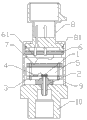
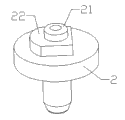
As shown in Figure 1, based on the media isolated pressure sensor of back side metallization technology, comprise sensor chip 1, chip mounting base 2, PCB lower plate 3, signal condition chip 4, PCB connector 5, PCB top board 6, PCB upper plate 7, electric interfaces 8, metal shell 9, pressure interface 10; Chip mounting base 2 is hollow structure, and there is through hole the centre, and sensor chip 1 is welded on the chip mounting base 2 through hole top face of weld 21, and chip mounting base 2 is bonding by glue and PCB lower plate 3; Signal condition chip 4 is mounted on the PCB lower plate 3, and signal condition chip 4 is by spun gold 41 and sensor chip 1 gold wire bonding; PCB upper plate 7 is connected by PCB connector 5 with PCB lower plate 3, and PCB upper plate 7 is connected with PCB top board 6 by flexible PCB 61, and PCB top board 6 is connected with electric interfaces 8; Chip mounting base 2 other ends are bonded on the pressure interface 10, and the end of chip mounting base 2 through holes is communicated with pressure interface 10, and pressure interface 10 is connected to integral body with electric interfaces 8 by metal shell 9.
Wherein, as shown in Figure 2, sensor chip 1 comprises silicon layer 11, glassy layer 12 and metal level 13, and metal level 13 is welded on the chip mounting base 2 through hole top face of weld 21 by the preformed solder reflow.
The metal level 13 of sensor chip 1 is to implant the golden or silver-colored of the about 400-1000nm of thickness 12 of glassy layers.
As shown in Figure 3 and Figure 4, face of weld 21 electrotinning nickel alloy layers on the chip mounting base 2.
As Fig. 3, Fig. 4 and shown in Figure 5, chip mounting base 2 has positioning boss 22 with PCB lower plate 3 bonding parts, and the hole shape in the middle of the PCB lower plate 3 is corresponding with it, guarantees the uniqueness of PCB lower plate 3 installation directions;
As shown in Figure 6 and Figure 7, PCB connector 5 comprises the wiring board contact pin 52 of connector shell 51 and both ends of the surface, and there is jack the position of PCB upper plate 7 and PCB lower plate 3 correspondences, has cavity to be used to hold sensor chip 1 in the connector shell 51.PCB installs by the PCB connector, only needs plug, need not welding.
As shown in Figure 8, electric interfaces 8 has reference column 84 and contact pin 83 with PCB top board 6 junctions, and there are positioning port and jack in the position of PCB top board 6 correspondences.Reference column has played the effect of location and anti-deflection in the installation process of electric interfaces, guaranteed to revolve the quality of riveter skill effectively, and contact pin is used for being electrically connected.
Claims (10)
1. based on the media isolated pressure sensor of back side metallization technology, it is characterized in that: comprise sensor chip (1), chip mounting base (2), PCB lower plate (3), signal condition chip (4), PCB connector (5), PCB top board (6), PCB upper plate (7), electric interfaces (8), metal shell (9), pressure interface (10); Chip mounting base (2) is hollow structure, and there is through hole the centre, and sensor chip (1) is welded on chip mounting base (2) the through hole top face of weld (21), and chip mounting base (2) is by in the hole in the middle of the bonding PCB lower plate of glue (3); Signal condition chip (4) is mounted on the PCB lower plate (3), and signal condition chip (4) is by spun gold (41) and sensor chip (1) gold wire bonding; PCB upper plate (7) is connected by PCB connector (5) with PCB lower plate (3), and PCB upper plate (7) is connected with PCB top board (6) by flexible PCB (61), and PCB top board (6) is connected with electric interfaces (8); Chip mounting base (2) other end is bonded on the pressure interface (10), and the end of chip mounting base (2) through hole is communicated with pressure interface (10), and pressure interface (10) is connected to integral body with electric interfaces (8) by metal shell (9).
2. the media isolated pressure sensor based on back side metallization technology according to claim 1, it is characterized in that: described sensor chip (1) comprises silicon layer (11), glassy layer (12) and metal level (13), and metal level (13) is welded on chip mounting base (2) the through hole top face of weld (21) by the preformed solder reflow.
3. the media isolated pressure sensor based on back side metallization technology according to claim 2 is characterized in that: the metal level (13) of described sensor chip (1) is for implanting the golden or silver-colored of the about 400-1000nm of thickness at glassy layer (12) face.
4. the media isolated pressure sensor based on back side metallization technology according to claim 1 is characterized in that: face of weld (21) the electrotinning nickel alloy layer of described chip mounting base (2).
5. the media isolated pressure sensor based on back side metallization technology according to claim 1, it is characterized in that: described pressure interface (10) is one with metal shell (9) by laser bonding, and O-ring seal (81) back of packing in the seal groove (82) in the electric interfaces (8) compresses by revolving the riveter skill with metal shell (9).
6. the media isolated pressure sensor based on back side metallization technology according to claim 1, it is characterized in that: described chip mounting base (2) has positioning boss (22) with PCB lower plate (3) bonding part, hole shape in the middle of the PCB lower plate (3) is corresponding with it, guarantees the uniqueness of PCB lower plate (3) installation direction.
7. according to claim 1,4 or 6 each described media isolated pressure sensor based on back side metallization technology, it is characterized in that: described chip mounting base (2) also has deep gouge (23) with PCB lower plate (3) bonding part, chip mounting base (2) has delta seal groove (24) with pressure interface (10) bonding part, increase effective bond area, strengthened glue-joint strength.
8. the media isolated pressure sensor based on back side metallization technology according to claim 1, it is characterized in that: described PCB connector (5) comprises the wiring board contact pin (52) of connector shell (51) and both ends of the surface, there is jack the corresponding position of PCB upper plate (7) and PCB lower plate (3), has cavity to be used to hold sensor chip (1) in the connector shell (51).
9. according to claim 1 or 5 based on the media isolated pressure sensor of back side metallization technology, it is characterized in that: electric interfaces (8) has reference column (84) and contact pin (83) with PCB top board (6) junction, and there are positioning port and jack in the position that PCB top board (6) is corresponding.
10. according to claim 1,4 or 6 described media isolated pressure sensor based on back side metallization technology, it is characterized in that: chip mounting base (2) adopts expansion alloy to process.
Priority Applications (1)
| Application Number | Priority Date | Filing Date | Title |
|---|---|---|---|
| CN2013101500005A CN103196623A (en) | 2013-04-26 | 2013-04-26 | Medium isolation pressure sensor based on back metalization process |
Applications Claiming Priority (1)
| Application Number | Priority Date | Filing Date | Title |
|---|---|---|---|
| CN2013101500005A CN103196623A (en) | 2013-04-26 | 2013-04-26 | Medium isolation pressure sensor based on back metalization process |
Publications (1)
| Publication Number | Publication Date |
|---|---|
| CN103196623A true CN103196623A (en) | 2013-07-10 |
Family
ID=48719318
Family Applications (1)
| Application Number | Title | Priority Date | Filing Date |
|---|---|---|---|
| CN2013101500005A Pending CN103196623A (en) | 2013-04-26 | 2013-04-26 | Medium isolation pressure sensor based on back metalization process |
Country Status (1)
| Country | Link |
|---|---|
| CN (1) | CN103196623A (en) |
Cited By (9)
| Publication number | Priority date | Publication date | Assignee | Title |
|---|---|---|---|---|
| CN103926029A (en) * | 2014-04-28 | 2014-07-16 | 中国电子科技集团公司第四十九研究所 | Method for air tightness hard packaging of sensitive chip of piezoresistive pressure sensor |
| CN105157904A (en) * | 2015-05-11 | 2015-12-16 | 中国电子科技集团公司第四十八研究所 | Anti-vibration pressure sensor resistant to transient oil pressure impact |
| CN105829851A (en) * | 2014-01-30 | 2016-08-03 | 日立汽车系统株式会社 | Mechanical quantity measuring device and sensor unit |
| CN109297633A (en) * | 2018-09-29 | 2019-02-01 | 宁波中车时代传感技术有限公司 | Pressure transmitter is used in a kind of monitoring of Cooling Water of Diesel Locomotive system pressure |
| CN110082009A (en) * | 2019-03-26 | 2019-08-02 | 南京史利姆电子科技有限公司 | A method of the fixed diffusion silicon chip of sealing |
| CN111492217A (en) * | 2018-05-17 | 2020-08-04 | 罗斯蒙特公司 | Measuring element and measuring device comprising such a measuring element |
| CN111707408A (en) * | 2020-07-08 | 2020-09-25 | 宁波中车时代传感技术有限公司 | Sputtering film pressure transmitter |
| CN114216519A (en) * | 2022-02-21 | 2022-03-22 | 深圳安培龙科技股份有限公司 | Temperature and pressure integrated sensor packaging structure |
| US11371899B2 (en) | 2018-05-17 | 2022-06-28 | Rosemount Inc. | Measuring element with an extended permeation resistant layer |
Citations (6)
| Publication number | Priority date | Publication date | Assignee | Title |
|---|---|---|---|---|
| JP2007132696A (en) * | 2005-11-08 | 2007-05-31 | Denso Corp | Pressure sensor and structure for mounting same |
| JP2010122036A (en) * | 2008-11-19 | 2010-06-03 | Denso Corp | Pressure sensor |
| CN201852666U (en) * | 2010-09-28 | 2011-06-01 | 刘胜 | Pressure transmitter of integrated pressure chip |
| CN102589787A (en) * | 2011-01-06 | 2012-07-18 | 霍尼韦尔国际公司 | Media isolated pressure sensor |
| CN202442825U (en) * | 2012-02-17 | 2012-09-19 | 苏州敏芯微电子技术有限公司 | Dielectric isolation encapsulating structure of pressure sensor |
| CN203231865U (en) * | 2013-04-26 | 2013-10-09 | 陈君杰 | Dielectric isolation pressure sensor based on backside metallization process |
-
2013
- 2013-04-26 CN CN2013101500005A patent/CN103196623A/en active Pending
Patent Citations (6)
| Publication number | Priority date | Publication date | Assignee | Title |
|---|---|---|---|---|
| JP2007132696A (en) * | 2005-11-08 | 2007-05-31 | Denso Corp | Pressure sensor and structure for mounting same |
| JP2010122036A (en) * | 2008-11-19 | 2010-06-03 | Denso Corp | Pressure sensor |
| CN201852666U (en) * | 2010-09-28 | 2011-06-01 | 刘胜 | Pressure transmitter of integrated pressure chip |
| CN102589787A (en) * | 2011-01-06 | 2012-07-18 | 霍尼韦尔国际公司 | Media isolated pressure sensor |
| CN202442825U (en) * | 2012-02-17 | 2012-09-19 | 苏州敏芯微电子技术有限公司 | Dielectric isolation encapsulating structure of pressure sensor |
| CN203231865U (en) * | 2013-04-26 | 2013-10-09 | 陈君杰 | Dielectric isolation pressure sensor based on backside metallization process |
Cited By (14)
| Publication number | Priority date | Publication date | Assignee | Title |
|---|---|---|---|---|
| CN105829851A (en) * | 2014-01-30 | 2016-08-03 | 日立汽车系统株式会社 | Mechanical quantity measuring device and sensor unit |
| CN105829851B (en) * | 2014-01-30 | 2018-06-15 | 日立汽车系统株式会社 | Mechanical measurement device |
| CN103926029B (en) * | 2014-04-28 | 2016-03-30 | 中国电子科技集团公司第四十九研究所 | The hard method for packing of piezoresistive pressure sensor sensitive chip impermeability |
| CN103926029A (en) * | 2014-04-28 | 2014-07-16 | 中国电子科技集团公司第四十九研究所 | Method for air tightness hard packaging of sensitive chip of piezoresistive pressure sensor |
| CN105157904A (en) * | 2015-05-11 | 2015-12-16 | 中国电子科技集团公司第四十八研究所 | Anti-vibration pressure sensor resistant to transient oil pressure impact |
| CN105157904B (en) * | 2015-05-11 | 2018-06-26 | 中国电子科技集团公司第四十八研究所 | A kind of resistance to instantaneous oil shock pressure sensor of anti-vibration |
| US11371899B2 (en) | 2018-05-17 | 2022-06-28 | Rosemount Inc. | Measuring element with an extended permeation resistant layer |
| CN111492217B (en) * | 2018-05-17 | 2022-09-09 | 罗斯蒙特公司 | Measuring element and measuring device comprising such a measuring element |
| CN111492217A (en) * | 2018-05-17 | 2020-08-04 | 罗斯蒙特公司 | Measuring element and measuring device comprising such a measuring element |
| CN109297633A (en) * | 2018-09-29 | 2019-02-01 | 宁波中车时代传感技术有限公司 | Pressure transmitter is used in a kind of monitoring of Cooling Water of Diesel Locomotive system pressure |
| CN110082009A (en) * | 2019-03-26 | 2019-08-02 | 南京史利姆电子科技有限公司 | A method of the fixed diffusion silicon chip of sealing |
| CN111707408A (en) * | 2020-07-08 | 2020-09-25 | 宁波中车时代传感技术有限公司 | Sputtering film pressure transmitter |
| CN114216519A (en) * | 2022-02-21 | 2022-03-22 | 深圳安培龙科技股份有限公司 | Temperature and pressure integrated sensor packaging structure |
| CN114216519B (en) * | 2022-02-21 | 2022-05-10 | 深圳安培龙科技股份有限公司 | Temperature and pressure integrated sensor packaging structure |
Similar Documents
| Publication | Publication Date | Title |
|---|---|---|
| CN103196623A (en) | Medium isolation pressure sensor based on back metalization process | |
| CN103487176B (en) | Structure and method for packaging pressure sensor | |
| US3817107A (en) | Semiconductor pressure transducer | |
| JP2010514180A (en) | Encapsulation module, method for its generation and use thereof | |
| US9406747B2 (en) | Component in the form of a wafer level package and method for manufacturing same | |
| CN102749159A (en) | Sensor device with sealing structure | |
| CN104030233A (en) | Top Port Mems Cavity Package | |
| CN203231865U (en) | Dielectric isolation pressure sensor based on backside metallization process | |
| JP2006090846A (en) | Pressure sensor | |
| KR20170096574A (en) | Pressure detecting unit and pressure sensor using the same | |
| US20210290929A1 (en) | Electronics module and arrangement for a ventricular assist device, and method for producing a ventricular assist device | |
| CN102275859A (en) | MEMS (micro electro mechanical system) microsensor encapsulation structure and manufacturing method thereof | |
| CN102928150A (en) | Leadless packaged metal film pressure sensor and preparation method thereof | |
| CN101652647B (en) | Connector unit for a pressure sensor | |
| CN105314588A (en) | Vertically hybridly integrated assembly having an interposer for stress-decoupling of a mems structure, and method for its manufacture | |
| US20140331776A1 (en) | Strain Gauge Pressure Sensor | |
| US20210041318A1 (en) | High temperature protected wire bonded sensors | |
| CN105789141A (en) | Micro-assembling miniaturized three-dimensional microwave circuit structure | |
| CN113526455A (en) | Packaging structure of MEMS pressure sensor | |
| CN202710237U (en) | Absolute pressure sensor packaging structure | |
| CN110672259A (en) | Packaging module and pressure sensor adopting same | |
| KR20180125515A (en) | Molded Interconnect Microelectromechanical Systems (MEMS) Device Package | |
| KR102242428B1 (en) | Strain gauge pressure sensor | |
| JP5804445B2 (en) | Semiconductor pressure sensor | |
| JP4901767B2 (en) | Pressure sensor and pressure sensor manufacturing method |
Legal Events
| Date | Code | Title | Description |
|---|---|---|---|
| C06 | Publication | ||
| PB01 | Publication | ||
| C10 | Entry into substantive examination | ||
| SE01 | Entry into force of request for substantive examination | ||
| C02 | Deemed withdrawal of patent application after publication (patent law 2001) | ||
| WD01 | Invention patent application deemed withdrawn after publication |
Application publication date: 20130710 |