EP3098866A1 - Piezoelectric power generation module and remote controller - Google Patents
Piezoelectric power generation module and remote controller Download PDFInfo
- Publication number
- EP3098866A1 EP3098866A1 EP14879607.1A EP14879607A EP3098866A1 EP 3098866 A1 EP3098866 A1 EP 3098866A1 EP 14879607 A EP14879607 A EP 14879607A EP 3098866 A1 EP3098866 A1 EP 3098866A1
- Authority
- EP
- European Patent Office
- Prior art keywords
- piezoelectric device
- piezoelectric
- power generation
- voltage
- switch control
- Prior art date
- Legal status (The legal status is an assumption and is not a legal conclusion. Google has not performed a legal analysis and makes no representation as to the accuracy of the status listed.)
- Granted
Links
Images


Classifications
-
- H—ELECTRICITY
- H02—GENERATION; CONVERSION OR DISTRIBUTION OF ELECTRIC POWER
- H02N—ELECTRIC MACHINES NOT OTHERWISE PROVIDED FOR
- H02N2/00—Electric machines in general using piezoelectric effect, electrostriction or magnetostriction
- H02N2/18—Electric machines in general using piezoelectric effect, electrostriction or magnetostriction producing electrical output from mechanical input, e.g. generators
- H02N2/181—Circuits; Control arrangements or methods
-
- G—PHYSICS
- G08—SIGNALLING
- G08C—TRANSMISSION SYSTEMS FOR MEASURED VALUES, CONTROL OR SIMILAR SIGNALS
- G08C17/00—Arrangements for transmitting signals characterised by the use of a wireless electrical link
- G08C17/02—Arrangements for transmitting signals characterised by the use of a wireless electrical link using a radio link
-
- G—PHYSICS
- G08—SIGNALLING
- G08C—TRANSMISSION SYSTEMS FOR MEASURED VALUES, CONTROL OR SIMILAR SIGNALS
- G08C2201/00—Transmission systems of control signals via wireless link
- G08C2201/10—Power supply of remote control devices
- G08C2201/11—Energy harvesting
- G08C2201/112—Mechanical energy, e.g. vibration, piezoelectric
-
- H—ELECTRICITY
- H10—SEMICONDUCTOR DEVICES; ELECTRIC SOLID-STATE DEVICES NOT OTHERWISE PROVIDED FOR
- H10N—ELECTRIC SOLID-STATE DEVICES NOT OTHERWISE PROVIDED FOR
- H10N30/00—Piezoelectric or electrostrictive devices
- H10N30/30—Piezoelectric or electrostrictive devices with mechanical input and electrical output, e.g. functioning as generators or sensors
- H10N30/304—Beam type
Definitions
- the present invention relates to a piezoelectric power generation module and to a remote controller including the same.
- the present invention relates to a piezoelectric power generation module that converts mechanical energy applied to a piezoelectric device into electrical energy and supplies power to a processing circuit, and relates to a remote controller.
- Patent Document 1 discloses a configuration of a remote controller which has a power generation capability and which, after detecting that an input unit depressed by the finger of a user has recovered, executes an input command.
- the remote controller converts AC power generated when the input unit is depressed and when the input unit recovers therefrom into DC power by using a rectifier unit, and stores the DC power in a power storage unit (capacitor).
- Patent Document 2 discloses a configuration in which AC power generated by letting the free end of an actuator freely vibrate is converted into DC power by a rectifier.
- Patent Document 1 and Patent Document 2 a charge generated by a piezoelectric device is moved through a full-wave rectifier circuit to a capacitor which is a power storage unit.
- a full-wave rectifier circuit can supply to a subsequent circuit both a charge generated at a positive potential obtained as a result of the piezoelectric device deforming to the first main surface side and a charge generated at a negative potential obtained as a result of the piezoelectric device deforming to the second main surface side when the plate-shaped piezoelectric device deforms.
- energy loss accompanying this movement of charges is generated in the full-wave rectifier circuit and, hence, there is a problem in that the ratio (energy efficiency) of available energy to generated energy is low.
- a piezoelectric power generation module based on the present invention includes: a piezoelectric device including a first terminal and a second terminal; a diode including a cathode connected to the first terminal of the piezoelectric device and an anode connected to the second terminal of the piezoelectric device; a switch control circuit including a first input terminal connected to the cathode, a second input terminal connected to the anode, and an output terminal outputting a switch control signal; and a first switch that is connected to the first input terminal of the switch control circuit and that switches between a conductive state and a cut off state in response to the switch control signal.
- the piezoelectric device is a power generating device
- the first switch enters a conductive state as a result of a voltage across the piezoelectric device exceeding a first threshold voltage larger than a reference potential, and the first switch enters a cut off state as a result of the voltage across the piezoelectric device becoming a second threshold voltage lower than the first threshold voltage.
- the piezoelectric device causes a voltage to be generated at the first terminal of the piezoelectric device as a result of a load being applied to the piezoelectric device, and the voltage across the piezoelectric device becomes the reference potential when the load applied to the piezoelectric device is released.
- the switch control circuit includes a comparator circuit and a temperature compensation device, and the temperature compensation device is connected in parallel with the first input terminal and the second input terminal of the switch control circuit.
- the switch control circuit further includes a second switch, the second switch is connected in parallel with the temperature compensation device, and the second switch switches between on and off in synchronization with a state of the first switch.
- the temperature dependency after a voltage at the first terminal of the piezoelectric device having become the first threshold voltage can be reduced and, hence, energy efficiency is further increased.
- the piezoelectric power generation module further includes a capacitor device connected in parallel with the first input terminal and the second input terminal of the switch control circuit.
- a remote controller based on the present invention includes the piezoelectric power generation module and an RF circuit, and the RF circuit performs communication processing during a period after a voltage at the first terminal of the piezoelectric device exceeds the first threshold voltage and before the voltage at the first terminal of the piezoelectric device reaches the second threshold voltage.
- a piezoelectric power generation module and a remote controller enabling stable driving and having satisfactory energy efficiency is realized.
- Fig. 1 is a circuit diagram of a piezoelectric power generation module 100 according to a first embodiment.
- the piezoelectric power generation module 100 includes a piezoelectric device 1, a diode 2, a load switch control circuit 3, a load switch 4, a first signal line Tpe1, a second signal line Tpe2, an output node N1, and an output node N2.
- a load 5 is connected between the output node N1 and the output node N2.
- the load 5 is a processing circuit such as an RF circuit, a microcomputer, or the like. These processing circuits are supplied with a power supply voltage from the output node N1 and the output node N2 of the piezoelectric power generation module 100, and output a signal (for example, an identification code ID) that controls an electronic apparatus located at a remote position.
- a remote controller or a wireless switch is realized.
- the load switch control circuit 3 corresponds to the switch control circuit of the present invention.
- the load switch 4 corresponds to the first switch of the present invention.
- Fig. 2(a) is a cross-sectional view schematically illustrating the state of the piezoelectric device 1 to which stress is not being applied.
- the piezoelectric device 1 includes a piezoelectric body 1C and a metal plate 1D.
- the piezoelectric body 1C is plate-shaped and is formed of, for example, a lead zirconate titanate ceramic.
- An electrode 1A is provided on one main surface of the piezoelectric body 1C, and an electrode 1B is provided on the other main surface.
- the metal plate 1D and the piezoelectric body 1C are electrically united with each other with the electrode 1B therebetween.
- the electrode 1A is connected to the first signal line Tpe1, and the metal plate 1D is connected to the second signal line Tpe2.
- the second signal line Tpe2 is connected to a reference potential (GND).
- the two ends of the piezoelectric device 1 are held by support units 1E.
- the piezoelectric device 1 is polarized in a direction indicated by the arrow illustrated in Fig. 2(b) .
- the electrode 1A corresponds to the first terminal of the piezoelectric device of the present invention.
- the electrode 1B corresponds to the second terminal of the piezoelectric device of the present invention.
- the diode 2 is, for example, a clamp diode.
- the anode and cathode of the diode 2 are respectively connected to the second signal line Tpe2 and the first signal line Tpe1 of the piezoelectric device 1.
- the diode 2 is connected in parallel with the piezoelectric device 1.
- the diode 2 is provided so that a voltage which is negative with respect to a reference potential, which is a potential in a state in which the piezoelectric device 1 is not deformed, is not applied to the load 5.
- a power supply node Nc1 and a power supply node Nc2 of the load switch control circuit 3 are respectively connected to the first signal line Tpe1 and the second signal line Tpe2 of the piezoelectric device 1.
- the first input terminal of the load switch 4 is connected to the power supply node Nc1 of the load switch control circuit 3.
- the second input terminal of the load switch 4 is connected to the power supply node Nc2.
- the load switch control circuit 3 outputs a load switch control signal S4 from the output terminal of the load switch 4 and switches between the conductive state and cut off state of the load switch 4.
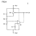
- Fig. 4 is a circuit diagram of the load switch control circuit 3 included in the piezoelectric power generation module 100 in Fig. 1 .
- the load switch control circuit 3 is formed of, for example, a CMOS circuit.
- the load switch control circuit 3 includes a first input terminal connected to the power supply node Nc1, a second input terminal connected to the power supply node Nc2, and an output terminal.
- the load switch control circuit 3 includes a resistor R1, a resistor R2, and a resistor R3, sequentially connected from the power supply node Nc1 side, between the power supply node Nc1 and the power supply node Nc2.
- the load switch control circuit 3 includes a switch 3A which is, for example, an electronic switch, a comparison voltage generation circuit 33 which is, for example, a band-gap reference, and a comparator circuit 32 which is, for example, an operational amplifier.
- One end of the resistor R1 is connected to the power supply node Nc1 and the other end is connected to one end of the resistor R2.
- the one end of the resistor R2 is connected to the other end of the resistor R1 and the other end of the resistor R2 is connected to one end of the resistor R3.
- the one end of the resistor R3 is connected to the other end of the resistor R2 and the other end of the resistor R3 is connected to the power supply node Nc2.
- One end of the switch 3A is connected to the power supply node Nc1 and the other end is connected to the other end of the resistor R1.
- the input terminal of the comparison voltage generation circuit 33 is connected to the power supply node Nc2 and the output terminal is connected to the inverting input terminal of the comparator circuit 32.
- the non-inverting input terminal of the comparator circuit 32 is connected to the one end of the resistor R3, and the output terminal is connected to the switch 3A and the load switch 4. Note that the switch 3A corresponds to the second switch of the present invention.
- the load switch control circuit 3 is set such that a change in the output logic level of the load switch control signal S4 for a change in a power generation voltage Vpe input between the power supply node Nc1 and the power supply node Nc2 has hysteresis characteristics.
- the hysteresis characteristics can be realized as a result of the conductive state of the switch 3A being switched by the load switch control signal S4 output by the comparator circuit 32.
- Fig. 2(b) schematically illustrates a sectional view of the piezoelectric device 1 in a state in which a load is applied thereto.
- Fig. 2(b) illustrates how the piezoelectric body 1C of the piezoelectric device 1 is polarized due to deformation caused by depression, how a positive charge accumulates on the electrode 1A connected to the first signal line Tpe1, and how a negative charge accumulates on the electrode 1B connected to the second signal line Tpe2.
- Fig. 2(c) illustrates how depression of the piezoelectric device 1 is being released, that is, how the piezoelectric device 1 is returning from the state illustrated in Fig. 2(b) to the state illustrated in Fig. 2(a) as a result of stress applied to the piezoelectric device 1 being released. It is illustrated, in the piezoelectric device 1 during releasing of depression, how a negative charge accumulates on the electrode 1A connected to the first signal line Tpe1 and a negative charge accumulates on the electrode 1B connected to the second signal line Tpe2, in the piezoelectric body 1C.
- the piezoelectric device 1 When the piezoelectric device 1 is depressed (stress is applied), in accordance with deformation of the piezoelectric device 1, the potential of the first signal line Tpe1 increases with respect to the potential of the second signal line Tpe2. The power generation voltage Vpe is generated on the first signal line Tpe1. On the other hand, when depression of the piezoelectric device 1 is released, the piezoelectric device 1 automatically returns to the initial state, and the power generation voltage Vpe of the first signal line Tpe1 becomes zero.
- the load switch control circuit 3 in Fig. 4 makes the logic level of the output load switch control signal S4 change in accordance with an increase or a decrease of the power generation voltage Vpe applied between the power supply node Nc1 and the power supply node Nc2.
- the load switch 4 is correspondingly set to a conductive state (on state) or a cut off state (off state).
- the load switch 4 is set to a conductive state, the power generation voltage Vpe generated between the output node N1 and the output node N2 is supplied to the load 5.
- the amount of charge stored in the piezoelectric device 1 gradually decreases, causing the value of the power generation voltage Vpe to be reduced.
- the potential of the power supply node Nc2 in a state in which the piezoelectric device is not deformed corresponds to the reference potential of the present invention.
- the load switch control circuit 3 is set such that a change in the logic level of the output load switch control signal S4 for a change in the input power generation voltage Vpe has hysteresis characteristics.
- the load switch 4 changes from a cut off state to a conductive state.
- the threshold voltage Vth corresponds to the first threshold voltage of the present invention
- the threshold voltage Vtl corresponds to the second threshold voltage of the present invention.
- the power generation voltage Vpe is divided by the resistor R1, the resistor R2, and the resistor R3 connected in series between the power supply node Nc1 and the power supply node Nc2.
- the comparator circuit 32 determines the logic level of the load switch control signal S4 by comparing the potential between the two ends of the resistor R3 with a potential generated by the comparison voltage generation circuit 33.
- the values of the resistors R1 to R3 and the value of the comparison voltage are appropriately set such that the threshold voltage Vth (refer to Fig. 1 ) has a target value.
- the resistors R1 to R3 connected in series with one another are connected in parallel with the piezoelectric device 1 and, hence, also function as a leak current path of the piezoelectric device 1.
- the values of the resistors R1 to R3 are set such that the value of a leak time constant is larger than the value of the charge time constant of the power generation voltage Vpe due to depression of the piezoelectric device 1.
- the comparator circuit 32 When the value of the power generation voltage Vpe exceeds the threshold voltage Vth, the comparator circuit 32 causes the logic level of the load switch control signal S4 to be changed from a low level to a high level. In response to this change in the load switch control signal S4, the load switch 4 is set to a conductive state, and the power generation voltage Vpe is applied to the output node N1 with the output node N2 as a reference (refer to Fig. 1 ).
- the switch 3A connected in parallel with the resistor R1 is also set to a conductive state, the voltage (power generation voltage Vpe) of the power supply node Nc1 is divided by the resistor R2 and the resistor R3.
- the comparator circuit 32 changes the logic level of the load switch control signal S4 from a high level to a low level.
- the load switch 4 is set to a cut off state and the supply of the power generation voltage Vpe to the output node N1 is stopped.
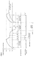
- Fig. 5 is a timing diagram describing the operation of the piezoelectric power generation module 100 in Fig. 1 .
- the operation of the piezoelectric power generation module 100 is described.
- the horizontal axis and the vertical axis respectively represent time and the power generation voltage Vpe schematically.
- the operations of the piezoelectric power generation module 100 illustrated in Fig. 5 are divided into operations as per the following three periods. 1) The first depression period when stress is applied to the piezoelectric device 1 from time t1 to time t2, 2) the period when depression of the piezoelectric device 1 is released from time t2 to time t3, and 3) the second depression period for depressing the piezoelectric device 1 from time t3 to time t4.
- the power generation voltage Vpe increases in accordance with an increase in distortion generated in the piezoelectric device 1.
- a time period T1 after time t1 when the value of the power generation voltage Vpe reaches the threshold voltage Vth, the load switch control circuit 3 changes the logic level of the load switch control signal S4 from a low level to a high level.
- the load switch 4 enters a conductive state and the piezoelectric power generation module 100 starts to supply the power generation voltage Vpe to the load 5.
- the load 5 consumes a charge stored in the piezoelectric device 1 during a time period T2 and performs predetermined processing (processing for transmitting a signal to an electronic apparatus).
- predetermined processing processing for transmitting a signal to an electronic apparatus.
- the value of the power generation voltage Vpe rapidly decreases to near the threshold voltage Vtl.
- the load 5 in an idling state consumes a charge, and at the end of the time period T3, the value of the power generation voltage Vpe reaches the threshold voltage Vt1.
- the load switch control circuit 3 makes the load switch 4 be in a cut off state by setting the logic level of the load switch control signal S4 to a low level, and stops supply of power to the load 5.
- second depression of the piezoelectric device 1 is started.
- the piezoelectric device similarly to the first depression period, increases the value of the power generation voltage Vpe from zero to the threshold voltage Vth.
- the piezoelectric power generation module 100 repeats operations of the time period T2 to the time period T6, similarly to the first depression period.
- the waveform of the power generation voltage Vpe denoted by a dotted line corresponds to a comparative example and is the waveform of the power generation voltage Vpe in the case where the diode 2 has been deleted from the piezoelectric power generation module 100.
- the effect of the diode 2 connected in parallel with the piezoelectric device 1 included in the piezoelectric power generation module 100 is described by comparing the waveform of the power generation voltage Vpe denoted by a dotted line, which is a comparative example, with the above-described waveform of the power generation voltage Vpe denoted by a solid line according to the first embodiment.
- the waveform of the power generation voltage Vpe during the first depression period from time t1 to time t2 and during the time period T5 included in the period of released depression according to the comparative example is the same as that of the first embodiment and, hence, the description thereof is omitted.
- the polarity of a charge generated in the piezoelectric device 1 is inverted, and the potential of the second signal line Tpe2 becomes higher than the potential of the first signal line Tpe1. In other words, the potential of Tpe2 becomes negative with respect to the reference potential.
- the stress applied to the piezoelectric device 1 at time t2 is the inverse of the stress applied to the piezoelectric device 1 during the time period T1.
- the value of the first signal line Tpe1 drops from the threshold voltage Vtl as much as the threshold voltage Vth.
- the value of the first signal line Tpe1 drops to a negative voltage with respect to the reference potential, i.e., a voltage equal to the threshold voltage Vth subtracted by the threshold voltage Vtl.
- the piezoelectric power generation module 100 includes the diode 2 connected in parallel with the piezoelectric device 1 and, hence, the charge stored by the piezoelectric device 1 after releasing of depression is released through discharging between the first signal line Tpe1 and the second signal line Tpe2 of the piezoelectric device 1.
- the piezoelectric device 1 even when the piezoelectric device 1 is depressed after releasing of depression, it becomes possible for the piezoelectric device 1 to generate the power generation voltage Vpe having a voltage necessary for a processing operation of the load 5.
- the piezoelectric power generation module 100 In the piezoelectric power generation module 100, DC power generated by the piezoelectric device 1 in a depressed state is supplied to the load 5, but DC power generated by the piezoelectric device 1 in which depression is released is not supplied to the load 5. Hence, unlike the existing signal generation apparatus in which AC power generated by a piezoelectric device in a depressed state and a depression-released state is converted into DC power by a full-wave rectifier circuit and supplied to a load, the piezoelectric power generation module 100 does not need a full-wave rectifier circuit (not illustrated) and a charge capacitor (not illustrated).
- charge movement energy loss generated in diodes for forming a full-wave rectifier circuit i.e., diodes connected in series between the piezoelectric device 1 and the load 5 is reduced.
- mechanical potential energy corresponding to the reduced charge movement energy loss is reduced, and a ratio of the load 5 consumption energy to the piezoelectric device 1 power generation energy, i.e., energy utilization efficiency is increased.
- the piezoelectric power generation module 100 that directly drives the load 5 using the piezoelectric device 1 without providing a charge capacitor can supply more charge energy to the load 5 than a general configuration including a rectifier circuit and a charge capacitor.
- the piezoelectric power generation module 100 includes the piezoelectric device 1 and the diode 2 connected in parallel with the piezoelectric device 1.
- the piezoelectric device 1 depressed to the lowest depression point usually outputs the power generation voltage Vpe having a value higher than or equal to the lowest operation voltage of the load 5, although depending on a balance between the amount of charge generated by the piezoelectric device 1 and charge consumption of the load 5.
- the potential of the first signal line Tpe1 decreases with respect to the second signal line Tpe2 to a negative value with respect to the reference potential, passing through the reference potential, i.e., zero, due to a charge generated in the piezoelectric device 1.
- the charge generated in the piezoelectric device 1 flows through the anode to cathode of the diode 2 and is consumed within the piezoelectric device 1, and the voltage of the first signal line Tpe1 of the piezoelectric device 1 is kept at zero also after releasing of depression.
- the piezoelectric device 1 depressed after releasing of depression again outputs the power generation voltage Vpe with a value higher than or equal to the lowest operation voltage of the load 5, whereby normal operation of the load 5 is secured.
- the load switch control circuit 3 sets the load switch 4 to a conductive state, and supplies a charge stored in the piezoelectric device 1 to the load 5.
- the load switch 4 is set to a cut off state and supply of a charge, i.e., power to the load 5 is stopped.
- Fig. 3 is a sectional view of a piezoelectric device 11 which is a modification of the piezoelectric device 1 in Fig. 2 .
- the piezoelectric device 11 has a configuration in which piezoelectric bodies 11C are stacked on top of one another such that charges having the same polarity are generated during depression at surfaces at which the piezoelectric bodies 11C face one another.
- the amount of charge generated by the piezoelectric device 11 is increased and the load 5 (refer to Fig. 1 ) can be driven for a longer time.
- the piezoelectric device 1 is formed of a lead zirconate titanate ceramic, but is not limited to this.
- the piezoelectric device 1 may be formed of a piezoelectric material which is a non-lead piezoelectric ceramic, such as a potassium sodium niobate ceramic or an alkali niobate-based ceramic.
- the support structure of the piezoelectric device 1 is formed of the two support units 1E, but is not limited to this.
- a configuration may be employed in which one end of the piezoelectric device 1 is held by a cantilever and stress is applied to the other end, which is a free end.
- the piezoelectric device 1 be shaped like a stick one end of which is held by a cantilever, stress is applied to the other end.
- the support structure of the piezoelectric device 1 need only have a configuration enabling deformation to be made by depression.
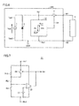
- Fig. 6 is a circuit diagram of a piezoelectric power generation module 200 according to a second embodiment.
- the piezoelectric power generation module 200 illustrated in Fig. 6 corresponds to a configuration obtained by replacing the load switch control circuit 3 in the piezoelectric power generation module 100 in Fig. 1 with a load switch control circuit 31.
- Fig. 7 is a circuit diagram of the load switch control circuit 31 in Fig. 6 .
- the load switch control circuit 31 in Fig. 7 corresponds to a configuration obtained by replacing the resistor R1 in the load switch control circuit 3 in Fig. 4 by a temperature compensation device R1S.
- the composition is usually adjusted to near a phase transition so as to increase power generation energy and, hence, the values of the capacitance and power generation voltage of the piezoelectric device 1 have considerable temperature characteristics.
- the dielectric constant of the piezoelectric body 1C has a positive temperature coefficient
- the capacitance value of the piezoelectric device 1 increases and the value of the power generation voltage Vpe of the piezoelectric device 1 decreases in accordance with an increase in the surrounding temperature.
- the value of the power generation voltage Vpe of the piezoelectric device 1 does not reach the threshold voltage Vth, and the load switch 4 is maintained in a cut off state, resulting in a problem in that the power generation voltage Vpe is not supplied to the load 5.
- a thermistor is applied to the temperature compensation device R1S, as a device having temperature characteristics in which the resistance value is negative.
- the resistance value of the temperature compensation device R1S decreases, and the potential at a connection point between the resistor R2 and the resistor R3 increases.
- the comparator circuit 32 causes the logic level of the load switch control signal S4 to be inverted, and the power generation voltage Vpe is supplied to the load 5.
- the value of the threshold voltage Vth set in the load switch control circuit 31 is given a negative temperature coefficient.
- a device whose resistance value has a positive temperature coefficient may be used as the temperature compensation device R1S, or, for example, a thermistor having a negative temperature coefficient may be used as R3.
- a configuration may be employed in which the comparison voltage generated by the comparison voltage generation circuit 33 has temperature dependency.
- the threshold voltage Vth varies with the temperature.
- the power generation voltage Vpe can be reliably supplied to the load 5 independently of the surrounding temperature. Note that in the embodiment described above, the resistor R1 in Fig. 4 has been replaced with the temperature compensation device R1S, but is not limited to this. Similar effect can be obtained also by replacing the resistor R2 or the resistor R3 in Fig. 4 with a temperature compensation device.
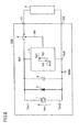
- Fig. 8 is a circuit diagram of a piezoelectric power generation module 300 according to a third embodiment.
- the piezoelectric power generation module 300 illustrated in Fig. 8 corresponds to a configuration obtained by connecting a storage capacitor 6 between the first signal wiring line Tpe1 and the second signal wiring line Tpe2 in the piezoelectric power generation module 100 illustrated in Fig. 1 .
- the storage capacitor 6 corresponds to the capacitor device of the present invention.
- the capacitance value and the value of the power generation voltage Vpe of the piezoelectric device 1 vary depending on the surrounding temperature in some cases. For example, in a low surrounding temperature range (temperature range lower than an ordinary temperature of 25°C), it is feared that an over voltage may be applied to the load 5 when the value of the power generation voltage Vpe increases more than in the case of ordinary temperature due to a decrease in the capacitance value of the piezoelectric device 1.
- a low surrounding temperature range temperature range lower than an ordinary temperature of 25°C
- an over voltage may be applied to the load 5 when the value of the power generation voltage Vpe increases more than in the case of ordinary temperature due to a decrease in the capacitance value of the piezoelectric device 1.
- the piezoelectric power generation module 300 has a configuration which is the combination of the storage capacitor 6 and the load switch control circuit 3 without temperature compensation of the threshold voltage Vth; however, the load switch control circuit 31 with temperature compensation of the threshold voltage Vth of the piezoelectric power generation module 200 illustrated in Fig. 6 may be combined with the storage capacitor 6. In that case, the undesirable problem which may appear in a high surrounding temperature range and the above-described undesirable problem of over voltage being applied which may appear in a low temperature range are solved.
Landscapes
- Engineering & Computer Science (AREA)
- Computer Networks & Wireless Communication (AREA)
- Physics & Mathematics (AREA)
- General Physics & Mathematics (AREA)
- General Electrical Machinery Utilizing Piezoelectricity, Electrostriction Or Magnetostriction (AREA)
Abstract
Description
- The present invention relates to a piezoelectric power generation module and to a remote controller including the same. For example, the present invention relates to a piezoelectric power generation module that converts mechanical energy applied to a piezoelectric device into electrical energy and supplies power to a processing circuit, and relates to a remote controller.
- Regarding a remote controller that includes a piezoelectric device and does not need a battery, a configuration is proposed that improves power generation efficiency. Japanese Unexamined Patent Application Publication No.
2011-103729 2004-201376 -
- Patent Document 1: Japanese Unexamined Patent Application Publication No.
2011-103729 - Patent Document 2: Japanese Unexamined Patent Application Publication No.
2004-201376 - In
Patent Document 1 andPatent Document 2, a charge generated by a piezoelectric device is moved through a full-wave rectifier circuit to a capacitor which is a power storage unit. With respect to a reference potential which is a potential in a state in which the piezoelectric device is not deformed, a full-wave rectifier circuit can supply to a subsequent circuit both a charge generated at a positive potential obtained as a result of the piezoelectric device deforming to the first main surface side and a charge generated at a negative potential obtained as a result of the piezoelectric device deforming to the second main surface side when the plate-shaped piezoelectric device deforms. However, energy loss accompanying this movement of charges is generated in the full-wave rectifier circuit and, hence, there is a problem in that the ratio (energy efficiency) of available energy to generated energy is low. Solution to Problem - A piezoelectric power generation module based on the present invention includes: a piezoelectric device including a first terminal and a second terminal; a diode including a cathode connected to the first terminal of the piezoelectric device and an anode connected to the second terminal of the piezoelectric device; a switch control circuit including a first input terminal connected to the cathode, a second input terminal connected to the anode, and an output terminal outputting a switch control signal; and a first switch that is connected to the first input terminal of the switch control circuit and that switches between a conductive state and a cut off state in response to the switch control signal.
- With this configuration, since a nonlinear device such as a diode is not provided in series between the piezoelectric device and the switch control circuit, energy loss encountered while a charge generated by the piezoelectric device moves can be reduced. Further, since a diode that clamps a voltage that is negative with respect to a reference potential is provided in parallel with the piezoelectric device between the piezoelectric device and the switch control circuit, the charge of the piezoelectric device can be quickly released when the voltage across the piezoelectric device becomes lower than or equal to the reference potential. This avoids a problem in that, even when a charge generated in the piezoelectric device for the first time is supplied to a subsequent stage, stable driving cannot be performed due to a decrease in the reference potential at a subsequent time. As a result, a piezoelectric power generation module enabling stable driving and having satisfactory energy efficiency is realized.
- Preferably, the piezoelectric device is a power generating device, and the first switch enters a conductive state as a result of a voltage across the piezoelectric device exceeding a first threshold voltage larger than a reference potential, and the first switch enters a cut off state as a result of the voltage across the piezoelectric device becoming a second threshold voltage lower than the first threshold voltage.
- Preferably, the piezoelectric device causes a voltage to be generated at the first terminal of the piezoelectric device as a result of a load being applied to the piezoelectric device, and the voltage across the piezoelectric device becomes the reference potential when the load applied to the piezoelectric device is released.
- Preferably, the switch control circuit includes a comparator circuit and a temperature compensation device, and the temperature compensation device is connected in parallel with the first input terminal and the second input terminal of the switch control circuit.
- As a result, the temperature dependency of generated energy and a power generation voltage can be reduced.
- Preferably, the switch control circuit further includes a second switch, the second switch is connected in parallel with the temperature compensation device, and the second switch switches between on and off in synchronization with a state of the first switch.
- As a result, the temperature dependency after a voltage at the first terminal of the piezoelectric device having become the first threshold voltage can be reduced and, hence, energy efficiency is further increased.
- Preferably, the piezoelectric power generation module further includes a capacitor device connected in parallel with the first input terminal and the second input terminal of the switch control circuit.
- As a result, a voltage supplied to a stage subsequent to the switch can be controlled more accurately.
- A remote controller based on the present invention includes the piezoelectric power generation module and an RF circuit, and the RF circuit performs communication processing during a period after a voltage at the first terminal of the piezoelectric device exceeds the first threshold voltage and before the voltage at the first terminal of the piezoelectric device reaches the second threshold voltage.
- With this configuration, since a nonlinear device such as a diode is not provided in series between the piezoelectric device and the switch control circuit, energy loss encountered while a charge generated by the piezoelectric device moves can be reduced. Further, since a diode that clamps a voltage that is negative with respect to a reference potential is provided in parallel with the piezoelectric device between the piezoelectric device and the switch control circuit, the charge of the piezoelectric device can be quickly released when the voltage across the piezoelectric device becomes lower than or equal to the reference potential. Hence, a remote controller enabling stable driving and having satisfactory energy efficiency is realized.
- A piezoelectric power generation module and a remote controller enabling stable driving and having satisfactory energy efficiency is realized.
-
- [
Fig. 1] Fig. 1 is a circuit diagram of a piezoelectric power generation module according to a first embodiment. - [
Fig. 2] Fig. 2 is a cross-sectional view illustrating the relationship between a state in which a piezoelectric device included in the piezoelectric power generation module according to the first embodiment is depressed and a generated charge. - [
Fig. 3] Fig. 3 is a sectional view of a modification of the piezoelectric device according to the first embodiment. - [
Fig. 4] Fig. 4 is a circuit diagram of a load switch control circuit included in the piezoelectric power generation module according to the first embodiment. - [
Fig. 5] Fig. 5 is a timing diagram illustrating the operation of the piezoelectric power generation module according to the first embodiment. - [
Fig. 6] Fig. 6 is a circuit diagram of a piezoelectric power generation module according to a second embodiment. - [
Fig. 7] Fig. 7 is a circuit diagram of a load switch control circuit according to the second embodiment. - [
Fig. 8] Fig. 8 is a circuit diagram of a piezoelectric power generation module according to a third embodiment. Description of Embodiments - Hereinafter, embodiments will be described with reference to the drawings. In the description of the embodiments, although the number of units and the amounts that may be used are referred to, the number of units and the amounts that may be used are not limited to these unless specifically described. In the drawings of the embodiments, it is assumed that identical reference symbols or numerals denote identical portions or corresponding portions. Further, in the descriptions of the embodiments, duplicated descriptions of portions and others denoted by the same reference symbols and the like are not repeated in some cases.
-
Fig. 1 is a circuit diagram of a piezoelectricpower generation module 100 according to a first embodiment. - The piezoelectric
power generation module 100 includes apiezoelectric device 1, adiode 2, a loadswitch control circuit 3, aload switch 4, a first signal line Tpe1, a second signal line Tpe2, an output node N1, and an output node N2. - A
load 5 is connected between the output node N1 and the output node N2. Theload 5 is a processing circuit such as an RF circuit, a microcomputer, or the like. These processing circuits are supplied with a power supply voltage from the output node N1 and the output node N2 of the piezoelectricpower generation module 100, and output a signal (for example, an identification code ID) that controls an electronic apparatus located at a remote position. Hence, as a result of theload 5 being connected to the piezoelectricpower generation module 100, a remote controller or a wireless switch is realized. Note that the loadswitch control circuit 3 corresponds to the switch control circuit of the present invention. Theload switch 4 corresponds to the first switch of the present invention. -
Fig. 2(a) is a cross-sectional view schematically illustrating the state of thepiezoelectric device 1 to which stress is not being applied. Thepiezoelectric device 1 includes a piezoelectric body 1C and ametal plate 1D. The piezoelectric body 1C is plate-shaped and is formed of, for example, a lead zirconate titanate ceramic. Anelectrode 1A is provided on one main surface of the piezoelectric body 1C, and anelectrode 1B is provided on the other main surface. In thepiezoelectric device 1, themetal plate 1D and the piezoelectric body 1C are electrically united with each other with theelectrode 1B therebetween. Theelectrode 1A is connected to the first signal line Tpe1, and themetal plate 1D is connected to the second signal line Tpe2. The second signal line Tpe2 is connected to a reference potential (GND). - As illustrated in
Fig. 2(b) , the two ends of thepiezoelectric device 1 are held bysupport units 1E. Thepiezoelectric device 1 is polarized in a direction indicated by the arrow illustrated inFig. 2(b) . Note that theelectrode 1A corresponds to the first terminal of the piezoelectric device of the present invention. Theelectrode 1B corresponds to the second terminal of the piezoelectric device of the present invention. - The
diode 2 is, for example, a clamp diode. The anode and cathode of thediode 2 are respectively connected to the second signal line Tpe2 and the first signal line Tpe1 of thepiezoelectric device 1. In other words, thediode 2 is connected in parallel with thepiezoelectric device 1. Thediode 2 is provided so that a voltage which is negative with respect to a reference potential, which is a potential in a state in which thepiezoelectric device 1 is not deformed, is not applied to theload 5. - A power supply node Nc1 and a power supply node Nc2 of the load
switch control circuit 3 are respectively connected to the first signal line Tpe1 and the second signal line Tpe2 of thepiezoelectric device 1. The first input terminal of theload switch 4 is connected to the power supply node Nc1 of the loadswitch control circuit 3. The second input terminal of theload switch 4 is connected to the power supply node Nc2. The loadswitch control circuit 3 outputs a load switch control signal S4 from the output terminal of theload switch 4 and switches between the conductive state and cut off state of theload switch 4. -
Fig. 4 is a circuit diagram of the loadswitch control circuit 3 included in the piezoelectricpower generation module 100 inFig. 1 . - The load
switch control circuit 3 is formed of, for example, a CMOS circuit. The loadswitch control circuit 3 includes a first input terminal connected to the power supply node Nc1, a second input terminal connected to the power supply node Nc2, and an output terminal. The loadswitch control circuit 3 includes a resistor R1, a resistor R2, and a resistor R3, sequentially connected from the power supply node Nc1 side, between the power supply node Nc1 and the power supply node Nc2. The loadswitch control circuit 3 includes aswitch 3A which is, for example, an electronic switch, a comparisonvoltage generation circuit 33 which is, for example, a band-gap reference, and acomparator circuit 32 which is, for example, an operational amplifier. - One end of the resistor R1 is connected to the power supply node Nc1 and the other end is connected to one end of the resistor R2. The one end of the resistor R2 is connected to the other end of the resistor R1 and the other end of the resistor R2 is connected to one end of the resistor R3. The one end of the resistor R3 is connected to the other end of the resistor R2 and the other end of the resistor R3 is connected to the power supply node Nc2. One end of the
switch 3A is connected to the power supply node Nc1 and the other end is connected to the other end of the resistor R1. - The input terminal of the comparison
voltage generation circuit 33 is connected to the power supply node Nc2 and the output terminal is connected to the inverting input terminal of thecomparator circuit 32. The non-inverting input terminal of thecomparator circuit 32 is connected to the one end of the resistor R3, and the output terminal is connected to theswitch 3A and theload switch 4. Note that theswitch 3A corresponds to the second switch of the present invention. - The load
switch control circuit 3 is set such that a change in the output logic level of the load switch control signal S4 for a change in a power generation voltage Vpe input between the power supply node Nc1 and the power supply node Nc2 has hysteresis characteristics. The hysteresis characteristics can be realized as a result of the conductive state of theswitch 3A being switched by the load switch control signal S4 output by thecomparator circuit 32. -
Fig. 2(b) schematically illustrates a sectional view of thepiezoelectric device 1 in a state in which a load is applied thereto. By depressing (applying stress to) the center portion of thepiezoelectric device 1, mechanical energy is converted into electrical energy.Fig. 2(b) illustrates how the piezoelectric body 1C of thepiezoelectric device 1 is polarized due to deformation caused by depression, how a positive charge accumulates on theelectrode 1A connected to the first signal line Tpe1, and how a negative charge accumulates on theelectrode 1B connected to the second signal line Tpe2. -
Fig. 2(c) illustrates how depression of thepiezoelectric device 1 is being released, that is, how thepiezoelectric device 1 is returning from the state illustrated inFig. 2(b) to the state illustrated inFig. 2(a) as a result of stress applied to thepiezoelectric device 1 being released. It is illustrated, in thepiezoelectric device 1 during releasing of depression, how a negative charge accumulates on theelectrode 1A connected to the first signal line Tpe1 and a negative charge accumulates on theelectrode 1B connected to the second signal line Tpe2, in the piezoelectric body 1C. - When the
piezoelectric device 1 is depressed (stress is applied), in accordance with deformation of thepiezoelectric device 1, the potential of the first signal line Tpe1 increases with respect to the potential of the second signal line Tpe2. The power generation voltage Vpe is generated on the first signal line Tpe1. On the other hand, when depression of thepiezoelectric device 1 is released, thepiezoelectric device 1 automatically returns to the initial state, and the power generation voltage Vpe of the first signal line Tpe1 becomes zero. - The load
switch control circuit 3 inFig. 4 , as described above, makes the logic level of the output load switch control signal S4 change in accordance with an increase or a decrease of the power generation voltage Vpe applied between the power supply node Nc1 and the power supply node Nc2. When the logic level of the load switch control signal S4 is set to a high level or a low level, theload switch 4 is correspondingly set to a conductive state (on state) or a cut off state (off state). When theload switch 4 is set to a conductive state, the power generation voltage Vpe generated between the output node N1 and the output node N2 is supplied to theload 5. As theload 5 consumes a current, the amount of charge stored in thepiezoelectric device 1 gradually decreases, causing the value of the power generation voltage Vpe to be reduced. Note that the potential of the power supply node Nc2 in a state in which the piezoelectric device is not deformed corresponds to the reference potential of the present invention. - The load
switch control circuit 3 is set such that a change in the logic level of the output load switch control signal S4 for a change in the input power generation voltage Vpe has hysteresis characteristics. When the value of the power generation voltage Vpe increases from zero to a threshold voltage Vth, theload switch 4 changes from a cut off state to a conductive state. After that, when the value of the power generation voltage Vpe drops to a threshold voltage Vtl lower than the threshold voltage Vth in accordance with supply of a current to theload 5, the state of theload switch 4 changes from a conductive state to a cut off state. Note that the threshold voltage Vth corresponds to the first threshold voltage of the present invention, and the threshold voltage Vtl corresponds to the second threshold voltage of the present invention. - When the
switch 3A is in a cut off state, the power generation voltage Vpe is divided by the resistor R1, the resistor R2, and the resistor R3 connected in series between the power supply node Nc1 and the power supply node Nc2. Thecomparator circuit 32 determines the logic level of the load switch control signal S4 by comparing the potential between the two ends of the resistor R3 with a potential generated by the comparisonvoltage generation circuit 33. - The values of the resistors R1 to R3 and the value of the comparison voltage are appropriately set such that the threshold voltage Vth (refer to
Fig. 1 ) has a target value. The resistors R1 to R3 connected in series with one another are connected in parallel with thepiezoelectric device 1 and, hence, also function as a leak current path of thepiezoelectric device 1. Hence, the values of the resistors R1 to R3 are set such that the value of a leak time constant is larger than the value of the charge time constant of the power generation voltage Vpe due to depression of thepiezoelectric device 1. - When the value of the power generation voltage Vpe exceeds the threshold voltage Vth, the
comparator circuit 32 causes the logic level of the load switch control signal S4 to be changed from a low level to a high level. In response to this change in the load switch control signal S4, theload switch 4 is set to a conductive state, and the power generation voltage Vpe is applied to the output node N1 with the output node N2 as a reference (refer toFig. 1 ). - When the load switch control signal S4 is set to a high level, the
switch 3A connected in parallel with the resistor R1 is also set to a conductive state, the voltage (power generation voltage Vpe) of the power supply node Nc1 is divided by the resistor R2 and the resistor R3. Compared with the case when theswitch 3A is in a cut off state, the value of the voltage across the resistor R3 is increased and, hence, when the value of the power generation voltage Vpe reaches the threshold voltage Vtl lower than the threshold voltage Vth, thecomparator circuit 32 changes the logic level of the load switch control signal S4 from a high level to a low level. In response to this change in the load switch control signal S4, theload switch 4 is set to a cut off state and the supply of the power generation voltage Vpe to the output node N1 is stopped. -
Fig. 5 is a timing diagram describing the operation of the piezoelectricpower generation module 100 inFig. 1 . - Referring to
Fig. 5 andFig. 1 , the operation of the piezoelectricpower generation module 100 is described. InFig. 5 , the horizontal axis and the vertical axis respectively represent time and the power generation voltage Vpe schematically. The operations of the piezoelectricpower generation module 100 illustrated inFig. 5 are divided into operations as per the following three periods. 1) The first depression period when stress is applied to thepiezoelectric device 1 from time t1 to time t2, 2) the period when depression of thepiezoelectric device 1 is released from time t2 to time t3, and 3) the second depression period for depressing thepiezoelectric device 1 from time t3 to time t4. - When depression of the
piezoelectric device 1 is started at time t1, the power generation voltage Vpe increases in accordance with an increase in distortion generated in thepiezoelectric device 1. A time period T1 after time t1, when the value of the power generation voltage Vpe reaches the threshold voltage Vth, the loadswitch control circuit 3 changes the logic level of the load switch control signal S4 from a low level to a high level. In response to this change in the load switch control signal S4, theload switch 4 enters a conductive state and the piezoelectricpower generation module 100 starts to supply the power generation voltage Vpe to theload 5. - The
load 5 consumes a charge stored in thepiezoelectric device 1 during a time period T2 and performs predetermined processing (processing for transmitting a signal to an electronic apparatus). At the end of the time period T2, the value of the power generation voltage Vpe rapidly decreases to near the threshold voltage Vtl. Over a time period T3, theload 5 in an idling state consumes a charge, and at the end of the time period T3, the value of the power generation voltage Vpe reaches the threshold voltage Vt1. When the power generation voltage Vpe reaches the threshold voltage Vtl at the start time of a time period T4, the loadswitch control circuit 3 makes theload switch 4 be in a cut off state by setting the logic level of the load switch control signal S4 to a low level, and stops supply of power to theload 5. - At time t2 when a time period T5 starts, when depression of the
piezoelectric device 1 is released, the polarity of a charge generated in thepiezoelectric device 1 is inverted, and the potential of the second signal line Tpe2 becomes higher than the potential of the first signal line Tpe1. In other words, the potential of the second signal line Tpe2 becomes negative with respect to the reference potential. Hence, the voltage is clamped as a result of a current flowing from the anode to the cathode of thediode 2, and the charge stored in thepiezoelectric device 1 is released through discharging. As a result, the value of the power generation voltage Vpe rapidly decreases from the threshold voltage Vtl to zero. The value of the power generation voltage Vpe is maintained at zero until the end of a time period T6, that is, at the end of a time period during which depression is released. - At time t3 when a time period T7 starts, second depression of the
piezoelectric device 1 is started. Thepiezoelectric device 1, similarly to the first depression period, increases the value of the power generation voltage Vpe from zero to the threshold voltage Vth. Also after the time period T7, the piezoelectricpower generation module 100 repeats operations of the time period T2 to the time period T6, similarly to the first depression period. - (Waveform for the case where the
diode 2 has been deleted from the piezoelectric power generation module 100) - In
Fig. 5 , the waveform of the power generation voltage Vpe denoted by a dotted line corresponds to a comparative example and is the waveform of the power generation voltage Vpe in the case where thediode 2 has been deleted from the piezoelectricpower generation module 100. Hereinafter, the effect of thediode 2 connected in parallel with thepiezoelectric device 1 included in the piezoelectricpower generation module 100 is described by comparing the waveform of the power generation voltage Vpe denoted by a dotted line, which is a comparative example, with the above-described waveform of the power generation voltage Vpe denoted by a solid line according to the first embodiment. - The waveform of the power generation voltage Vpe during the first depression period from time t1 to time t2 and during the time period T5 included in the period of released depression according to the comparative example is the same as that of the first embodiment and, hence, the description thereof is omitted.
- When depression of the
piezoelectric device 1 is released at time t2 when the time period T5 starts, the polarity of a charge generated in thepiezoelectric device 1 is inverted, and the potential of the second signal line Tpe2 becomes higher than the potential of the first signal line Tpe1. In other words, the potential of Tpe2 becomes negative with respect to the reference potential. The stress applied to thepiezoelectric device 1 at time t2 is the inverse of the stress applied to thepiezoelectric device 1 during the time period T1. - Hence, a charge which can generate the threshold voltage Vth between the first signal line Tpe1 and the second signal line Tpe2 is induced in the
piezoelectric device 1 in which depression is released. As a result, after time t2, the value of the first signal line Tpe1 drops from the threshold voltage Vtl as much as the threshold voltage Vth. In other words, the value of the first signal line Tpe1 drops to a negative voltage with respect to the reference potential, i.e., a voltage equal to the threshold voltage Vth subtracted by the threshold voltage Vtl. - When second depression is started at time t3, the voltage of the first signal line Tpe1 starts to increase from a voltage which is negative with respect to the reference potential described above and, hence, cannot reach the threshold voltage Vtl. Hence, the load
switch control circuit 3 cannot make theload switch 4 be in a conductive state. As a result, supply of an electrode to theload 5 cannot be performed, and theload 5 cannot perform desired processing even when thepiezoelectric device 1 is depressed. - On the other hand, the piezoelectric
power generation module 100 according to the first embodiment includes thediode 2 connected in parallel with thepiezoelectric device 1 and, hence, the charge stored by thepiezoelectric device 1 after releasing of depression is released through discharging between the first signal line Tpe1 and the second signal line Tpe2 of thepiezoelectric device 1. As a result, even when thepiezoelectric device 1 is depressed after releasing of depression, it becomes possible for thepiezoelectric device 1 to generate the power generation voltage Vpe having a voltage necessary for a processing operation of theload 5. - The effect of the piezoelectric
power generation module 100 according to the first embodiment will be described. - In the piezoelectric
power generation module 100, DC power generated by thepiezoelectric device 1 in a depressed state is supplied to theload 5, but DC power generated by thepiezoelectric device 1 in which depression is released is not supplied to theload 5. Hence, unlike the existing signal generation apparatus in which AC power generated by a piezoelectric device in a depressed state and a depression-released state is converted into DC power by a full-wave rectifier circuit and supplied to a load, the piezoelectricpower generation module 100 does not need a full-wave rectifier circuit (not illustrated) and a charge capacitor (not illustrated). - By removing the full-wave rectifier circuit, charge movement energy loss generated in diodes for forming a full-wave rectifier circuit, i.e., diodes connected in series between the
piezoelectric device 1 and theload 5 is reduced. In other words, mechanical potential energy corresponding to the reduced charge movement energy loss is reduced, and a ratio of theload 5 consumption energy to thepiezoelectric device 1 power generation energy, i.e., energy utilization efficiency is increased. - Further, by removing the charge capacitor, energy loss caused by charge movement is reduced. When the equivalent capacitance value of the
piezoelectric device 1 is Cs, the amount of generated charge is Qs, and the capacitance value of the charge capacitor is Cc, charge energy P1 is given byEquation 1. On the other hand, charge energy P2 in the case of only thepiezoelectric device 1 is given byEquation 2.

- Since P1 < P2, the piezoelectric
power generation module 100 that directly drives theload 5 using thepiezoelectric device 1 without providing a charge capacitor can supply more charge energy to theload 5 than a general configuration including a rectifier circuit and a charge capacitor. - The piezoelectric
power generation module 100 includes thepiezoelectric device 1 and thediode 2 connected in parallel with thepiezoelectric device 1. Thepiezoelectric device 1 depressed to the lowest depression point usually outputs the power generation voltage Vpe having a value higher than or equal to the lowest operation voltage of theload 5, although depending on a balance between the amount of charge generated by thepiezoelectric device 1 and charge consumption of theload 5. When depression is released after the processing operation of theload 5, the potential of the first signal line Tpe1 decreases with respect to the second signal line Tpe2 to a negative value with respect to the reference potential, passing through the reference potential, i.e., zero, due to a charge generated in thepiezoelectric device 1. - Then, the charge generated in the
piezoelectric device 1 flows through the anode to cathode of thediode 2 and is consumed within thepiezoelectric device 1, and the voltage of the first signal line Tpe1 of thepiezoelectric device 1 is kept at zero also after releasing of depression. As a result, thepiezoelectric device 1 depressed after releasing of depression, again outputs the power generation voltage Vpe with a value higher than or equal to the lowest operation voltage of theload 5, whereby normal operation of theload 5 is secured. - When the value of the power generation voltage Vpe of the
piezoelectric device 1 exceeds the threshold voltage Vth, the loadswitch control circuit 3 sets theload switch 4 to a conductive state, and supplies a charge stored in thepiezoelectric device 1 to theload 5. After that, when the value of the power generation voltage Vpe becomes lower than the threshold voltage Vtl, which is set to be lower than the value of the threshold voltage Vth, due to power consumption of theload 5 or releasing of depression of thepiezoelectric device 1, theload switch 4 is set to a cut off state and supply of a charge, i.e., power to theload 5 is stopped. - In this way, as a result of setting being performed such that a change in the conductive state of the
load switch 4 has hysteresis characteristics with respect to a change in the input power generation voltage Vpe, power is supplied to theload 5 and the response of a remote controller including the piezoelectricpower generation module 100 is speeded up through a single depressing operation onto thepiezoelectric device 1. -
Fig. 3 is a sectional view of apiezoelectric device 11 which is a modification of thepiezoelectric device 1 inFig. 2 . - In
Fig. 3 , components denoted by the same symbols as those inFig. 2 have the same configurations or functions as those inFig. 2 and duplicated descriptions thereof are omitted. InFig. 3 , thepiezoelectric device 11 has a configuration in which piezoelectric bodies 11C are stacked on top of one another such that charges having the same polarity are generated during depression at surfaces at which the piezoelectric bodies 11C face one another. As a result of thepiezoelectric body 11 having a stacked configuration, the amount of charge generated by thepiezoelectric device 11 is increased and the load 5 (refer toFig. 1 ) can be driven for a longer time. - Note that in the embodiments described above, the
piezoelectric device 1 is formed of a lead zirconate titanate ceramic, but is not limited to this. For example, thepiezoelectric device 1 may be formed of a piezoelectric material which is a non-lead piezoelectric ceramic, such as a potassium sodium niobate ceramic or an alkali niobate-based ceramic. - Further, in the embodiments described above, the support structure of the
piezoelectric device 1 is formed of the twosupport units 1E, but is not limited to this. For example a configuration may be employed in which one end of thepiezoelectric device 1 is held by a cantilever and stress is applied to the other end, which is a free end. Alternatively, by making thepiezoelectric device 1 be shaped like a stick one end of which is held by a cantilever, stress is applied to the other end. In other words, the support structure of thepiezoelectric device 1 need only have a configuration enabling deformation to be made by depression. -
Fig. 6 is a circuit diagram of a piezoelectricpower generation module 200 according to a second embodiment. - In
Fig. 6 , components denoted by the same symbols as those inFig. 1 have the same configurations or functions of those inFig. 1 and duplicated descriptions thereof are omitted. The piezoelectricpower generation module 200 illustrated inFig. 6 corresponds to a configuration obtained by replacing the loadswitch control circuit 3 in the piezoelectricpower generation module 100 inFig. 1 with a loadswitch control circuit 31. -
Fig. 7 is a circuit diagram of the loadswitch control circuit 31 inFig. 6 . - The load
switch control circuit 31 inFig. 7 corresponds to a configuration obtained by replacing the resistor R1 in the loadswitch control circuit 3 inFig. 4 by a temperature compensation device R1S. - In the piezoelectric device 1 (refer to
Fig. 2 ) that uses, for example, PZT (lead zirconate titanate) for the piezoelectric body 1C, the composition is usually adjusted to near a phase transition so as to increase power generation energy and, hence, the values of the capacitance and power generation voltage of thepiezoelectric device 1 have considerable temperature characteristics. When the dielectric constant of the piezoelectric body 1C has a positive temperature coefficient, the capacitance value of thepiezoelectric device 1 increases and the value of the power generation voltage Vpe of thepiezoelectric device 1 decreases in accordance with an increase in the surrounding temperature. As a result, in a high surrounding temperature range (temperature range higher than an ordinary temperature of 25°C), the value of the power generation voltage Vpe of thepiezoelectric device 1 does not reach the threshold voltage Vth, and theload switch 4 is maintained in a cut off state, resulting in a problem in that the power generation voltage Vpe is not supplied to theload 5. - Hence, in the load
switch control circuit 31 inFig. 7 , for example, a thermistor is applied to the temperature compensation device R1S, as a device having temperature characteristics in which the resistance value is negative. In accordance with an increase in the surrounding temperature, the resistance value of the temperature compensation device R1S decreases, and the potential at a connection point between the resistor R2 and the resistor R3 increases. As a result, even in a high surrounding temperature range, thecomparator circuit 32 causes the logic level of the load switch control signal S4 to be inverted, and the power generation voltage Vpe is supplied to theload 5. In other words, due to the temperature compensation device R1S having characteristics with a negative resistance value, the value of the threshold voltage Vth set in the loadswitch control circuit 31 is given a negative temperature coefficient. - Note that in the case where the dielectric constant of the piezoelectric body 1C has a negative temperature coefficient, a device whose resistance value has a positive temperature coefficient may be used as the temperature compensation device R1S, or, for example, a thermistor having a negative temperature coefficient may be used as R3. Further, instead of making the value of the resistor R1 (refer to
Fig. 4 ) have temperature dependency, a configuration may be employed in which the comparison voltage generated by the comparisonvoltage generation circuit 33 has temperature dependency. - By employing a temperature compensation device for the value of the threshold voltage set in the load
switch control circuit 31, the threshold voltage Vth varies with the temperature. As a result, even in the case where the capacitance value of thepiezoelectric device 1 changes with temperature, the power generation voltage Vpe can be reliably supplied to theload 5 independently of the surrounding temperature. Note that in the embodiment described above, the resistor R1 inFig. 4 has been replaced with the temperature compensation device R1S, but is not limited to this. Similar effect can be obtained also by replacing the resistor R2 or the resistor R3 inFig. 4 with a temperature compensation device. -
Fig. 8 is a circuit diagram of a piezoelectricpower generation module 300 according to a third embodiment. - In
Fig. 8 , components denoted by the same symbols as those inFig. 1 have the same configurations or functions of those inFig. 1 and duplicated descriptions thereof are omitted. The piezoelectricpower generation module 300 illustrated inFig. 8 corresponds to a configuration obtained by connecting astorage capacitor 6 between the first signal wiring line Tpe1 and the second signal wiring line Tpe2 in the piezoelectricpower generation module 100 illustrated inFig. 1 . Note that thestorage capacitor 6 corresponds to the capacitor device of the present invention. - As described above, the capacitance value and the value of the power generation voltage Vpe of the
piezoelectric device 1 vary depending on the surrounding temperature in some cases. For example, in a low surrounding temperature range (temperature range lower than an ordinary temperature of 25°C), it is feared that an over voltage may be applied to theload 5 when the value of the power generation voltage Vpe increases more than in the case of ordinary temperature due to a decrease in the capacitance value of thepiezoelectric device 1. By connecting thestorage capacitor 6 in parallel with thepiezoelectric device 1, the charge generated by thepiezoelectric device 1 is distributed to thepiezoelectric device 1 and thestorage capacitor 6, and an increase in the power generation voltage Vpe is suppressed. - The piezoelectric
power generation module 300 has a configuration which is the combination of thestorage capacitor 6 and the loadswitch control circuit 3 without temperature compensation of the threshold voltage Vth; however, the loadswitch control circuit 31 with temperature compensation of the threshold voltage Vth of the piezoelectricpower generation module 200 illustrated inFig. 6 may be combined with thestorage capacitor 6. In that case, the undesirable problem which may appear in a high surrounding temperature range and the above-described undesirable problem of over voltage being applied which may appear in a low temperature range are solved. - The embodiments disclosed here are illustrative in all points and are not considered to be restrictive. The scope of the present invention is shown by the claims, and it is intended that all the modifications that have equivalent meanings and that are within the scope of the claims are included.
-
- 1
- piezoelectric device
- 1A
- electrode
- 1B
- electrode
- 1C
- piezoelectric body
- 1D
- metal plate
- 1E
- support unit
- 2
- diode
- 3
- load switch control circuit
- 4
- load switch
- 5
- load
- 6
- storage capacitor
- 11
- piezoelectric body
- 11C
- piezoelectric bodies
- 3A
- switch
- 31
- load switch control circuit
- 32
- comparator circuit
- 33
- comparison voltage generation circuit
- 100
- piezoelectric power generation module
- 200
- piezoelectric power generation module
- 300
- piezoelectric power generation module
- GND
- reference potential
- N1, N2
- output nodes
- Nc1, Nc2
- power supply nodes
- R1-R3
- resistors
- R1S
- temperature compensation device
- S4
- load switch control signal
- Tpe1
- first signal line
- Tpe2
- second signal line
- Vpe
- power generation voltage
- Vth, Vtl
- threshold voltages
Claims (7)
- A piezoelectric power generation module comprising:a piezoelectric device including a first terminal and a second terminal;a diode including a cathode connected to the first terminal of the piezoelectric device and an anode connected to the second terminal of the piezoelectric device;a switch control circuit including a first input terminal connected to the cathode, a second input terminal connected to the anode, and an output terminal outputting a switch control signal; anda first switch that is connected to the first input terminal of the switch control circuit and that switches between a conductive state and a cut off state in response to the switch control signal.
- The piezoelectric power generation module according to Claim 1,
wherein the piezoelectric device is a power generating device, and the first switch enters a conductive state as a result of a voltage across the piezoelectric device exceeding a first threshold voltage larger than a reference potential, and
wherein the first switch enters a cut off state as a result of the voltage across the piezoelectric device becoming a second threshold voltage lower than the first threshold voltage. - The piezoelectric power generation module according to Claim 1 or 2,
wherein the piezoelectric device causes a voltage to be generated at the first terminal of the piezoelectric device as a result of a load being applied to the piezoelectric device, and the voltage across the piezoelectric device becomes the reference potential when the load applied to the piezoelectric device is released. - The piezoelectric power generation module according to any one of Claims 1 to 3,
wherein the switch control circuit includes a comparator circuit and a temperature compensation device, and the temperature compensation device is connected in parallel with the first input terminal and the second input terminal of the switch control circuit. - The piezoelectric power generation module according to Claim 4,
wherein the switch control circuit further includes a second switch,
wherein the second switch is connected in parallel with the temperature compensation device, and
wherein the second switch switches between on and off in synchronization with a state of the first switch. - The piezoelectric power generation module according to any one of Claim 1 to Claim 5, further comprising a capacitor device connected in parallel with the first input terminal and the second input terminal of the switch control circuit.
- A remote controller comprising:the piezoelectric power generation module according to any one of Claim 1 to Claim 6; andan RF circuit,wherein the RF circuit performs communication processing during a period after a voltage at the first terminal of the piezoelectric device exceeds the first threshold voltage and before the voltage at the first terminal of the piezoelectric device reaches the second threshold voltage.
Applications Claiming Priority (2)
| Application Number | Priority Date | Filing Date | Title |
|---|---|---|---|
| JP2014009596 | 2014-01-22 | ||
| PCT/JP2014/077669 WO2015111258A1 (en) | 2014-01-22 | 2014-10-17 | Piezoelectric power generation module and remote controller |
Publications (3)
| Publication Number | Publication Date |
|---|---|
| EP3098866A1 true EP3098866A1 (en) | 2016-11-30 |
| EP3098866A4 EP3098866A4 (en) | 2017-11-29 |
| EP3098866B1 EP3098866B1 (en) | 2020-02-12 |
Family
ID=53681081
Family Applications (1)
| Application Number | Title | Priority Date | Filing Date |
|---|---|---|---|
| EP14879607.1A Active EP3098866B1 (en) | 2014-01-22 | 2014-10-17 | Piezoelectric power generation module and remote controller |
Country Status (5)
| Country | Link |
|---|---|
| US (1) | US9882511B2 (en) |
| EP (1) | EP3098866B1 (en) |
| JP (1) | JP6098736B2 (en) |
| CN (1) | CN105849925B (en) |
| WO (1) | WO2015111258A1 (en) |
Families Citing this family (11)
| Publication number | Priority date | Publication date | Assignee | Title |
|---|---|---|---|---|
| JP6089947B2 (en) * | 2013-05-13 | 2017-03-08 | 住友電気工業株式会社 | Radio apparatus and radio control system |
| CN105556825B (en) * | 2013-08-13 | 2018-03-13 | 国立大学法人东北大学 | power generation device |
| CN105850026B (en) * | 2014-01-22 | 2018-06-12 | 株式会社村田制作所 | Piezoelectric generator module and remote control |
| JP6406538B2 (en) * | 2014-06-17 | 2018-10-17 | Toto株式会社 | Remote control device for toilet equipment |
| JP6497265B2 (en) * | 2015-08-06 | 2019-04-10 | 株式会社デンソー | Vehicle collision detection device |
| WO2017104342A1 (en) * | 2015-12-15 | 2017-06-22 | 株式会社村田製作所 | Power generation device and transmitter comprising same |
| JP2019034430A (en) * | 2017-08-10 | 2019-03-07 | 東芝テック株式会社 | Printer apparatus and program |
| JP6872031B2 (en) * | 2017-10-02 | 2021-05-19 | アルプスアルパイン株式会社 | Input device |
| CN107818683B (en) * | 2017-11-28 | 2024-03-26 | 广东工业大学 | A wireless control switch device and system |
| KR102097222B1 (en) * | 2018-12-27 | 2020-04-06 | 주식회사 두산 | Resin composition, metal laminate and printed circuit board using the same, and method for manufacturing the metal laminate |
| TWD224316S (en) | 2021-09-24 | 2023-03-21 | 律盟風險管理顧問股份有限公司 | Graphical user interface of computer program product |
Family Cites Families (20)
| Publication number | Priority date | Publication date | Assignee | Title |
|---|---|---|---|---|
| JPH07245970A (en) * | 1994-03-02 | 1995-09-19 | Calsonic Corp | Piezoelectric power generator |
| JP3274047B2 (en) * | 1995-10-05 | 2002-04-15 | 株式会社豊田中央研究所 | Driving device and driving method for piezoelectric actuator |
| JP3539138B2 (en) * | 1997-06-24 | 2004-07-07 | ミノルタ株式会社 | Drive circuit for drive device using electromechanical transducer |
| US6259372B1 (en) * | 1999-01-22 | 2001-07-10 | Eaton Corporation | Self-powered wireless transducer |
| FR2802731B1 (en) * | 1999-12-16 | 2002-01-25 | Schneider Electric Ind Sa | AUTONOMOUS REMOTE CONTROL DEVICE, APPARATUS AND ELECTRICAL INSTALLATION COMPRISING SUCH A DEVICE |
| US6630894B1 (en) * | 2000-07-14 | 2003-10-07 | Face International Corp. | Self-powered switching device |
| JP2003007491A (en) * | 2001-06-26 | 2003-01-10 | Nec Tokin Ceramics Corp | Luminescence substance lighting equipment |
| WO2003025969A1 (en) | 2001-09-12 | 2003-03-27 | Jisouken Co., Ltd. | Power source apparatus |
| JP2004103265A (en) * | 2002-09-05 | 2004-04-02 | Nec Tokin Corp | Luminous unit and luminous shoes using the same |
| JP3616386B2 (en) | 2002-12-17 | 2005-02-02 | 太平洋セメント株式会社 | Signal transmitter |
| US7132939B2 (en) * | 2004-07-07 | 2006-11-07 | Michelin Recherche Et Technique S.A. | Integrated self-powered tire revolution counter |
| FR2896635A1 (en) * | 2006-01-23 | 2007-07-27 | Commissariat Energie Atomique | METHOD AND DEVICE FOR CONVERTING MECHANICAL ENERGY INTO ELECTRICAL ENERGY |
| US7781943B1 (en) * | 2007-01-24 | 2010-08-24 | Micro Strain, Inc. | Capacitive discharge energy harvesting converter |
| US20080252174A1 (en) * | 2007-04-10 | 2008-10-16 | Advanced Cerametrics, Inc. | Energy harvesting from multiple piezoelectric sources |
| JP5530155B2 (en) | 2009-11-11 | 2014-06-25 | ルネサスエレクトロニクス株式会社 | Manual operation equipment with power generation function, remote control device with power generation function |
| JP5979353B2 (en) * | 2011-05-06 | 2016-08-24 | セイコーエプソン株式会社 | Power generation device, electronic device, moving means and battery |
| US8653718B2 (en) * | 2011-05-06 | 2014-02-18 | Seiko Epson Corporation | Power generation unit, electronic apparatus, transportation unit, battery, method of controlling power generation unit |
| JP5807743B2 (en) | 2011-10-03 | 2015-11-10 | セイコーエプソン株式会社 | POWER GENERATION DEVICE, ELECTRONIC DEVICE, MOBILE DEVICE, AND POWER GENERATION DEVICE CONTROL METHOD |
| JP2013038941A (en) * | 2011-08-09 | 2013-02-21 | Nippon Dengyo Kosaku Co Ltd | Charge voltage control circuit and power supply circuit |
| JP5879887B2 (en) * | 2011-10-03 | 2016-03-08 | セイコーエプソン株式会社 | Power generator |
-
2014
- 2014-10-17 JP JP2015558733A patent/JP6098736B2/en active Active
- 2014-10-17 CN CN201480071275.2A patent/CN105849925B/en active Active
- 2014-10-17 WO PCT/JP2014/077669 patent/WO2015111258A1/en not_active Ceased
- 2014-10-17 EP EP14879607.1A patent/EP3098866B1/en active Active
-
2016
- 2016-06-30 US US15/198,382 patent/US9882511B2/en active Active
Also Published As
| Publication number | Publication date |
|---|---|
| US20160308469A1 (en) | 2016-10-20 |
| US9882511B2 (en) | 2018-01-30 |
| JP6098736B2 (en) | 2017-03-22 |
| WO2015111258A1 (en) | 2015-07-30 |
| EP3098866B1 (en) | 2020-02-12 |
| CN105849925B (en) | 2018-12-25 |
| EP3098866A4 (en) | 2017-11-29 |
| CN105849925A (en) | 2016-08-10 |
| JPWO2015111258A1 (en) | 2017-03-23 |
Similar Documents
| Publication | Publication Date | Title |
|---|---|---|
| EP3098866B1 (en) | Piezoelectric power generation module and remote controller | |
| Du et al. | A cold-startup SSHI rectifier for piezoelectric energy harvesters with increased open-circuit voltage | |
| US11664749B2 (en) | Power supply circuit and vibration-driven energy harvester | |
| US20120280596A1 (en) | Power generation unit, electronic apparatus, transportation unit, battery, method of controlling power generation unit | |
| US10008961B2 (en) | Power generating device | |
| CN102136800A (en) | Switch regulator | |
| JP6623189B2 (en) | Power supply circuit and power supply device | |
| US20140062389A1 (en) | Power generator, secondary cell, electronic apparatus, and transporter | |
| US10014801B2 (en) | Piezoelectric power generation module and remote controller | |
| US11424673B2 (en) | Power supply circuit, start-up circuit, power generating device, and electronic apparatus | |
| JP6499036B2 (en) | Power storage device and wireless system | |
| JP6481773B2 (en) | Power generation device and transmitter having the same | |
| WO2012101683A1 (en) | Sawtooth wave generation circuit | |
| JP6540803B2 (en) | POWER GENERATOR AND ELECTRICAL EQUIPMENT COMPRISING THE SAME | |
| JP2018148763A (en) | Dielectric elastomer power generation system | |
| CN210016394U (en) | Sawtooth wave oscillator of DC/DC switching power supply | |
| Dallago et al. | Comparison of two autonomous AC-DC converters for piezoelectric energy scavenging systems | |
| JP5319404B2 (en) | Power converter | |
| JP2019205329A (en) | Power inverter circuit and electric power unit | |
| JP2016058695A (en) | Electronic devices |
Legal Events
| Date | Code | Title | Description |
|---|---|---|---|
| PUAI | Public reference made under article 153(3) epc to a published international application that has entered the european phase |
Free format text: ORIGINAL CODE: 0009012 |
|
| 17P | Request for examination filed |
Effective date: 20160603 |
|
| AK | Designated contracting states |
Kind code of ref document: A1 Designated state(s): AL AT BE BG CH CY CZ DE DK EE ES FI FR GB GR HR HU IE IS IT LI LT LU LV MC MK MT NL NO PL PT RO RS SE SI SK SM TR |
|
| AX | Request for extension of the european patent |
Extension state: BA ME |
|
| DAX | Request for extension of the european patent (deleted) | ||
| RIC1 | Information provided on ipc code assigned before grant |
Ipc: H01L 41/04 20060101AFI20170810BHEP Ipc: H01L 41/083 20060101ALI20170810BHEP Ipc: H01L 41/113 20060101ALI20170810BHEP Ipc: H02N 2/18 20060101ALI20170810BHEP |
|
| A4 | Supplementary search report drawn up and despatched |
Effective date: 20171102 |
|
| RIC1 | Information provided on ipc code assigned before grant |
Ipc: H02N 2/18 20060101ALI20171025BHEP Ipc: H01L 41/04 20060101AFI20171025BHEP Ipc: H01L 41/113 20060101ALI20171025BHEP Ipc: H01L 41/083 20060101ALI20171025BHEP |
|
| GRAP | Despatch of communication of intention to grant a patent |
Free format text: ORIGINAL CODE: EPIDOSNIGR1 |
|
| STAA | Information on the status of an ep patent application or granted ep patent |
Free format text: STATUS: GRANT OF PATENT IS INTENDED |
|
| INTG | Intention to grant announced |
Effective date: 20190828 |
|
| GRAS | Grant fee paid |
Free format text: ORIGINAL CODE: EPIDOSNIGR3 |
|
| GRAA | (expected) grant |
Free format text: ORIGINAL CODE: 0009210 |
|
| STAA | Information on the status of an ep patent application or granted ep patent |
Free format text: STATUS: THE PATENT HAS BEEN GRANTED |
|
| AK | Designated contracting states |
Kind code of ref document: B1 Designated state(s): AL AT BE BG CH CY CZ DE DK EE ES FI FR GB GR HR HU IE IS IT LI LT LU LV MC MK MT NL NO PL PT RO RS SE SI SK SM TR |
|
| REG | Reference to a national code |
Ref country code: GB Ref legal event code: FG4D |
|
| REG | Reference to a national code |
Ref country code: CH Ref legal event code: EP |
|
| REG | Reference to a national code |
Ref country code: AT Ref legal event code: REF Ref document number: 1233255 Country of ref document: AT Kind code of ref document: T Effective date: 20200215 |
|
| REG | Reference to a national code |
Ref country code: IE Ref legal event code: FG4D |
|
| REG | Reference to a national code |
Ref country code: DE Ref legal event code: R096 Ref document number: 602014061073 Country of ref document: DE |
|
| PG25 | Lapsed in a contracting state [announced via postgrant information from national office to epo] |
Ref country code: NO Free format text: LAPSE BECAUSE OF FAILURE TO SUBMIT A TRANSLATION OF THE DESCRIPTION OR TO PAY THE FEE WITHIN THE PRESCRIBED TIME-LIMIT Effective date: 20200512 Ref country code: FI Free format text: LAPSE BECAUSE OF FAILURE TO SUBMIT A TRANSLATION OF THE DESCRIPTION OR TO PAY THE FEE WITHIN THE PRESCRIBED TIME-LIMIT Effective date: 20200212 Ref country code: RS Free format text: LAPSE BECAUSE OF FAILURE TO SUBMIT A TRANSLATION OF THE DESCRIPTION OR TO PAY THE FEE WITHIN THE PRESCRIBED TIME-LIMIT Effective date: 20200212 |
|
| REG | Reference to a national code |
Ref country code: LT Ref legal event code: MG4D |
|
| REG | Reference to a national code |
Ref country code: NL Ref legal event code: MP Effective date: 20200212 |
|
| PG25 | Lapsed in a contracting state [announced via postgrant information from national office to epo] |
Ref country code: BG Free format text: LAPSE BECAUSE OF FAILURE TO SUBMIT A TRANSLATION OF THE DESCRIPTION OR TO PAY THE FEE WITHIN THE PRESCRIBED TIME-LIMIT Effective date: 20200512 Ref country code: GR Free format text: LAPSE BECAUSE OF FAILURE TO SUBMIT A TRANSLATION OF THE DESCRIPTION OR TO PAY THE FEE WITHIN THE PRESCRIBED TIME-LIMIT Effective date: 20200513 Ref country code: IS Free format text: LAPSE BECAUSE OF FAILURE TO SUBMIT A TRANSLATION OF THE DESCRIPTION OR TO PAY THE FEE WITHIN THE PRESCRIBED TIME-LIMIT Effective date: 20200612 Ref country code: LV Free format text: LAPSE BECAUSE OF FAILURE TO SUBMIT A TRANSLATION OF THE DESCRIPTION OR TO PAY THE FEE WITHIN THE PRESCRIBED TIME-LIMIT Effective date: 20200212 Ref country code: SE Free format text: LAPSE BECAUSE OF FAILURE TO SUBMIT A TRANSLATION OF THE DESCRIPTION OR TO PAY THE FEE WITHIN THE PRESCRIBED TIME-LIMIT Effective date: 20200212 Ref country code: HR Free format text: LAPSE BECAUSE OF FAILURE TO SUBMIT A TRANSLATION OF THE DESCRIPTION OR TO PAY THE FEE WITHIN THE PRESCRIBED TIME-LIMIT Effective date: 20200212 |
|
| PG25 | Lapsed in a contracting state [announced via postgrant information from national office to epo] |
Ref country code: NL Free format text: LAPSE BECAUSE OF FAILURE TO SUBMIT A TRANSLATION OF THE DESCRIPTION OR TO PAY THE FEE WITHIN THE PRESCRIBED TIME-LIMIT Effective date: 20200212 |
|
| PG25 | Lapsed in a contracting state [announced via postgrant information from national office to epo] |
Ref country code: ES Free format text: LAPSE BECAUSE OF FAILURE TO SUBMIT A TRANSLATION OF THE DESCRIPTION OR TO PAY THE FEE WITHIN THE PRESCRIBED TIME-LIMIT Effective date: 20200212 Ref country code: PT Free format text: LAPSE BECAUSE OF FAILURE TO SUBMIT A TRANSLATION OF THE DESCRIPTION OR TO PAY THE FEE WITHIN THE PRESCRIBED TIME-LIMIT Effective date: 20200705 Ref country code: LT Free format text: LAPSE BECAUSE OF FAILURE TO SUBMIT A TRANSLATION OF THE DESCRIPTION OR TO PAY THE FEE WITHIN THE PRESCRIBED TIME-LIMIT Effective date: 20200212 Ref country code: SK Free format text: LAPSE BECAUSE OF FAILURE TO SUBMIT A TRANSLATION OF THE DESCRIPTION OR TO PAY THE FEE WITHIN THE PRESCRIBED TIME-LIMIT Effective date: 20200212 Ref country code: RO Free format text: LAPSE BECAUSE OF FAILURE TO SUBMIT A TRANSLATION OF THE DESCRIPTION OR TO PAY THE FEE WITHIN THE PRESCRIBED TIME-LIMIT Effective date: 20200212 Ref country code: CZ Free format text: LAPSE BECAUSE OF FAILURE TO SUBMIT A TRANSLATION OF THE DESCRIPTION OR TO PAY THE FEE WITHIN THE PRESCRIBED TIME-LIMIT Effective date: 20200212 Ref country code: DK Free format text: LAPSE BECAUSE OF FAILURE TO SUBMIT A TRANSLATION OF THE DESCRIPTION OR TO PAY THE FEE WITHIN THE PRESCRIBED TIME-LIMIT Effective date: 20200212 Ref country code: SM Free format text: LAPSE BECAUSE OF FAILURE TO SUBMIT A TRANSLATION OF THE DESCRIPTION OR TO PAY THE FEE WITHIN THE PRESCRIBED TIME-LIMIT Effective date: 20200212 Ref country code: EE Free format text: LAPSE BECAUSE OF FAILURE TO SUBMIT A TRANSLATION OF THE DESCRIPTION OR TO PAY THE FEE WITHIN THE PRESCRIBED TIME-LIMIT Effective date: 20200212 |
|
| REG | Reference to a national code |
Ref country code: DE Ref legal event code: R097 Ref document number: 602014061073 Country of ref document: DE |
|
| REG | Reference to a national code |
Ref country code: AT Ref legal event code: MK05 Ref document number: 1233255 Country of ref document: AT Kind code of ref document: T Effective date: 20200212 |
|
| PLBE | No opposition filed within time limit |
Free format text: ORIGINAL CODE: 0009261 |
|
| STAA | Information on the status of an ep patent application or granted ep patent |
Free format text: STATUS: NO OPPOSITION FILED WITHIN TIME LIMIT |
|
| 26N | No opposition filed |
Effective date: 20201113 |
|
| PG25 | Lapsed in a contracting state [announced via postgrant information from national office to epo] |
Ref country code: IT Free format text: LAPSE BECAUSE OF FAILURE TO SUBMIT A TRANSLATION OF THE DESCRIPTION OR TO PAY THE FEE WITHIN THE PRESCRIBED TIME-LIMIT Effective date: 20200212 Ref country code: AT Free format text: LAPSE BECAUSE OF FAILURE TO SUBMIT A TRANSLATION OF THE DESCRIPTION OR TO PAY THE FEE WITHIN THE PRESCRIBED TIME-LIMIT Effective date: 20200212 |
|
| PG25 | Lapsed in a contracting state [announced via postgrant information from national office to epo] |
Ref country code: PL Free format text: LAPSE BECAUSE OF FAILURE TO SUBMIT A TRANSLATION OF THE DESCRIPTION OR TO PAY THE FEE WITHIN THE PRESCRIBED TIME-LIMIT Effective date: 20200212 Ref country code: SI Free format text: LAPSE BECAUSE OF FAILURE TO SUBMIT A TRANSLATION OF THE DESCRIPTION OR TO PAY THE FEE WITHIN THE PRESCRIBED TIME-LIMIT Effective date: 20200212 |
|
| REG | Reference to a national code |
Ref country code: CH Ref legal event code: PL |
|
| GBPC | Gb: european patent ceased through non-payment of renewal fee |
Effective date: 20201017 |
|
| PG25 | Lapsed in a contracting state [announced via postgrant information from national office to epo] |
Ref country code: MC Free format text: LAPSE BECAUSE OF FAILURE TO SUBMIT A TRANSLATION OF THE DESCRIPTION OR TO PAY THE FEE WITHIN THE PRESCRIBED TIME-LIMIT Effective date: 20200212 Ref country code: LU Free format text: LAPSE BECAUSE OF NON-PAYMENT OF DUE FEES Effective date: 20201017 |
|
| REG | Reference to a national code |
Ref country code: BE Ref legal event code: MM Effective date: 20201031 |
|
| PG25 | Lapsed in a contracting state [announced via postgrant information from national office to epo] |
Ref country code: FR Free format text: LAPSE BECAUSE OF NON-PAYMENT OF DUE FEES Effective date: 20201031 |
|
| PG25 | Lapsed in a contracting state [announced via postgrant information from national office to epo] |
Ref country code: LI Free format text: LAPSE BECAUSE OF NON-PAYMENT OF DUE FEES Effective date: 20201031 Ref country code: GB Free format text: LAPSE BECAUSE OF NON-PAYMENT OF DUE FEES Effective date: 20201017 Ref country code: CH Free format text: LAPSE BECAUSE OF NON-PAYMENT OF DUE FEES Effective date: 20201031 Ref country code: BE Free format text: LAPSE BECAUSE OF NON-PAYMENT OF DUE FEES Effective date: 20201031 |
|
| PG25 | Lapsed in a contracting state [announced via postgrant information from national office to epo] |
Ref country code: IE Free format text: LAPSE BECAUSE OF NON-PAYMENT OF DUE FEES Effective date: 20201017 |
|
| PG25 | Lapsed in a contracting state [announced via postgrant information from national office to epo] |
Ref country code: TR Free format text: LAPSE BECAUSE OF FAILURE TO SUBMIT A TRANSLATION OF THE DESCRIPTION OR TO PAY THE FEE WITHIN THE PRESCRIBED TIME-LIMIT Effective date: 20200212 Ref country code: MT Free format text: LAPSE BECAUSE OF FAILURE TO SUBMIT A TRANSLATION OF THE DESCRIPTION OR TO PAY THE FEE WITHIN THE PRESCRIBED TIME-LIMIT Effective date: 20200212 Ref country code: CY Free format text: LAPSE BECAUSE OF FAILURE TO SUBMIT A TRANSLATION OF THE DESCRIPTION OR TO PAY THE FEE WITHIN THE PRESCRIBED TIME-LIMIT Effective date: 20200212 |
|
| PG25 | Lapsed in a contracting state [announced via postgrant information from national office to epo] |
Ref country code: MK Free format text: LAPSE BECAUSE OF FAILURE TO SUBMIT A TRANSLATION OF THE DESCRIPTION OR TO PAY THE FEE WITHIN THE PRESCRIBED TIME-LIMIT Effective date: 20200212 Ref country code: AL Free format text: LAPSE BECAUSE OF FAILURE TO SUBMIT A TRANSLATION OF THE DESCRIPTION OR TO PAY THE FEE WITHIN THE PRESCRIBED TIME-LIMIT Effective date: 20200212 |
|
| REG | Reference to a national code |
Ref country code: DE Ref legal event code: R079 Ref document number: 602014061073 Country of ref document: DE Free format text: PREVIOUS MAIN CLASS: H01L0041040000 Ipc: H10N0030800000 |
|
| PGFP | Annual fee paid to national office [announced via postgrant information from national office to epo] |
Ref country code: DE Payment date: 20251021 Year of fee payment: 12 |