EP3096356A1 - Semiconductor devices with vertical field floating rings and methods of fabrication thereof - Google Patents
Semiconductor devices with vertical field floating rings and methods of fabrication thereof Download PDFInfo
- Publication number
- EP3096356A1 EP3096356A1 EP16170099.2A EP16170099A EP3096356A1 EP 3096356 A1 EP3096356 A1 EP 3096356A1 EP 16170099 A EP16170099 A EP 16170099A EP 3096356 A1 EP3096356 A1 EP 3096356A1
- Authority
- EP
- European Patent Office
- Prior art keywords
- region
- epitaxial layer
- buried
- conductivity type
- semiconductor substrate
- Prior art date
- Legal status (The legal status is an assumption and is not a legal conclusion. Google has not performed a legal analysis and makes no representation as to the accuracy of the status listed.)
- Granted
Links
Images


Classifications
-
- H—ELECTRICITY
- H10—SEMICONDUCTOR DEVICES; ELECTRIC SOLID-STATE DEVICES NOT OTHERWISE PROVIDED FOR
- H10D—INORGANIC ELECTRIC SEMICONDUCTOR DEVICES
- H10D30/00—Field-effect transistors [FET]
- H10D30/60—Insulated-gate field-effect transistors [IGFET]
- H10D30/64—Double-diffused metal-oxide semiconductor [DMOS] FETs
- H10D30/65—Lateral DMOS [LDMOS] FETs
-
- H—ELECTRICITY
- H10—SEMICONDUCTOR DEVICES; ELECTRIC SOLID-STATE DEVICES NOT OTHERWISE PROVIDED FOR
- H10D—INORGANIC ELECTRIC SEMICONDUCTOR DEVICES
- H10D30/00—Field-effect transistors [FET]
- H10D30/01—Manufacture or treatment
- H10D30/021—Manufacture or treatment of FETs having insulated gates [IGFET]
-
- H—ELECTRICITY
- H10—SEMICONDUCTOR DEVICES; ELECTRIC SOLID-STATE DEVICES NOT OTHERWISE PROVIDED FOR
- H10D—INORGANIC ELECTRIC SEMICONDUCTOR DEVICES
- H10D30/00—Field-effect transistors [FET]
- H10D30/01—Manufacture or treatment
- H10D30/021—Manufacture or treatment of FETs having insulated gates [IGFET]
- H10D30/028—Manufacture or treatment of FETs having insulated gates [IGFET] of double-diffused metal oxide semiconductor [DMOS] FETs
- H10D30/0281—Manufacture or treatment of FETs having insulated gates [IGFET] of double-diffused metal oxide semiconductor [DMOS] FETs of lateral DMOS [LDMOS] FETs
-
- H—ELECTRICITY
- H10—SEMICONDUCTOR DEVICES; ELECTRIC SOLID-STATE DEVICES NOT OTHERWISE PROVIDED FOR
- H10D—INORGANIC ELECTRIC SEMICONDUCTOR DEVICES
- H10D62/00—Semiconductor bodies, or regions thereof, of devices having potential barriers
- H10D62/10—Shapes, relative sizes or dispositions of the regions of the semiconductor bodies; Shapes of the semiconductor bodies
- H10D62/102—Constructional design considerations for preventing surface leakage or controlling electric field concentration
- H10D62/103—Constructional design considerations for preventing surface leakage or controlling electric field concentration for increasing or controlling the breakdown voltage of reverse-biased devices
-
- H—ELECTRICITY
- H10—SEMICONDUCTOR DEVICES; ELECTRIC SOLID-STATE DEVICES NOT OTHERWISE PROVIDED FOR
- H10D—INORGANIC ELECTRIC SEMICONDUCTOR DEVICES
- H10D62/00—Semiconductor bodies, or regions thereof, of devices having potential barriers
- H10D62/10—Shapes, relative sizes or dispositions of the regions of the semiconductor bodies; Shapes of the semiconductor bodies
- H10D62/102—Constructional design considerations for preventing surface leakage or controlling electric field concentration
- H10D62/103—Constructional design considerations for preventing surface leakage or controlling electric field concentration for increasing or controlling the breakdown voltage of reverse-biased devices
- H10D62/105—Constructional design considerations for preventing surface leakage or controlling electric field concentration for increasing or controlling the breakdown voltage of reverse-biased devices by having particular doping profiles, shapes or arrangements of PN junctions; by having supplementary regions, e.g. junction termination extension [JTE]
- H10D62/106—Constructional design considerations for preventing surface leakage or controlling electric field concentration for increasing or controlling the breakdown voltage of reverse-biased devices by having particular doping profiles, shapes or arrangements of PN junctions; by having supplementary regions, e.g. junction termination extension [JTE] having supplementary regions doped oppositely to or in rectifying contact with regions of the semiconductor bodies, e.g. guard rings with PN or Schottky junctions
- H10D62/107—Buried supplementary regions, e.g. buried guard rings
-
- H—ELECTRICITY
- H10—SEMICONDUCTOR DEVICES; ELECTRIC SOLID-STATE DEVICES NOT OTHERWISE PROVIDED FOR
- H10D—INORGANIC ELECTRIC SEMICONDUCTOR DEVICES
- H10D62/00—Semiconductor bodies, or regions thereof, of devices having potential barriers
- H10D62/10—Shapes, relative sizes or dispositions of the regions of the semiconductor bodies; Shapes of the semiconductor bodies
- H10D62/17—Semiconductor regions connected to electrodes not carrying current to be rectified, amplified or switched, e.g. channel regions
- H10D62/351—Substrate regions of field-effect devices
- H10D62/357—Substrate regions of field-effect devices of FETs
- H10D62/364—Substrate regions of field-effect devices of FETs of IGFETs
- H10D62/371—Inactive supplementary semiconductor regions, e.g. for preventing punch-through, improving capacity effect or leakage current
-
- H—ELECTRICITY
- H10—SEMICONDUCTOR DEVICES; ELECTRIC SOLID-STATE DEVICES NOT OTHERWISE PROVIDED FOR
- H10D—INORGANIC ELECTRIC SEMICONDUCTOR DEVICES
- H10D62/00—Semiconductor bodies, or regions thereof, of devices having potential barriers
- H10D62/10—Shapes, relative sizes or dispositions of the regions of the semiconductor bodies; Shapes of the semiconductor bodies
- H10D62/17—Semiconductor regions connected to electrodes not carrying current to be rectified, amplified or switched, e.g. channel regions
- H10D62/393—Body regions of DMOS transistors or IGBTs
-
- H—ELECTRICITY
- H10—SEMICONDUCTOR DEVICES; ELECTRIC SOLID-STATE DEVICES NOT OTHERWISE PROVIDED FOR
- H10D—INORGANIC ELECTRIC SEMICONDUCTOR DEVICES
- H10D64/00—Electrodes of devices having potential barriers
- H10D64/111—Field plates
- H10D64/112—Field plates comprising multiple field plate segments
-
- H—ELECTRICITY
- H10—SEMICONDUCTOR DEVICES; ELECTRIC SOLID-STATE DEVICES NOT OTHERWISE PROVIDED FOR
- H10D—INORGANIC ELECTRIC SEMICONDUCTOR DEVICES
- H10D64/00—Electrodes of devices having potential barriers
- H10D64/20—Electrodes characterised by their shapes, relative sizes or dispositions
- H10D64/23—Electrodes carrying the current to be rectified, amplified, oscillated or switched, e.g. sources, drains, anodes or cathodes
- H10D64/251—Source or drain electrodes for field-effect devices
- H10D64/254—Source or drain electrodes for field-effect devices for lateral devices wherein the source or drain electrodes extend entirely through the semiconductor bodies, e.g. via-holes for back side contacts
Definitions
- Embodiments relate generally to semiconductor devices, and more specifically to lateral semiconductor devices, such as laterally diffused metal oxide semiconductor (LDMOS) field effect transistors (FETs).
- LDMOS laterally diffused metal oxide semiconductor
- FETs field effect transistors
- Integrated circuits (ICs) and other electronic devices often include arrangements of interconnected field-effect transistors (FETs), also called metal-oxide-semiconductor field-effect transistors (MOSFETs), or simply MOS transistors or devices.
- FETs field-effect transistors
- MOSFETs metal-oxide-semiconductor field-effect transistors
- a typical MOS transistor includes a gate electrode and spaced-apart source and drain electrodes. A control voltage applied to the gate electrode controls the flow of current through a variably conductive channel between the source and drain electrodes.
- Power transistor devices are designed to be tolerant of the high currents and voltages that are present in some applications. Some power transistor devices are also designed to handle radio frequency (RF) signals, such as the devices used in wireless communications and other RF power amplifier applications.
- RF power transistor device is a laterally diffused metal-oxide-semiconductor (LDMOS) transistor.
- LDMOS laterally diffused metal-oxide-semiconductor
- charge carriers drift through a drift space between a channel region and the drain electrode under the electric field arising from an operating voltage applied between the source and drain electrodes.
- the output power density and linear efficiency of an RF LDMOS transistor is affected by the transistor's drain-source capacitance, (C ds ), drain-gate capacitance (C dg ), on-state drain-to-source resistance (R dson ), and source-to-drain breakdown voltage (BV dss ).
- C ds drain-source capacitance
- C dg drain-gate capacitance
- R dson on-state drain-to-source resistance
- BV dss source-to-drain breakdown voltage
- An embodiment of an LDMOS transistor includes a substrate having a first conductivity type, and at least one buried region having a second conductivity type in a portion of the substrate that is below and vertically aligned with a drain region of the transistor.
- the buried region(s) help to stretch the depletion line deeper into the semiconductor substrate than may be achieved using a conventional device that lacks the aforementioned buried region(s).
- LDMOS devices with such buried region(s) may have a relatively low drain-to-gate capacitance (Cdg) and drain-to-source capacitance (Cds), when compared with conventional devices.
- LDMOS devices with such buried region(s) also may have a relatively high source-to-drain breakdown voltage (BVdss) and relatively low on-state drain-to-source resistance (Rdson), when compared with conventional devices.
- BVdss source-to-drain breakdown voltage
- Rdson on-state drain-to-source resistance
- an LDMOS device also may have a relatively deep high voltage region of a conductivity type opposite the substrate conductivity type (e.g., an n-type or NHV region) buried under the drain contact and extending towards the gate.
- a deep high voltage region is merged with a shallow high voltage region in order to form a drift region.
- the relatively deep, composite high voltage region may enable a conventional scaling plateau between BVdss and drift length to be broken, resulting in a higher BVdss while keeping Rdson relatively low, when compared with conventional devices that lack such a high voltage region.
- an LDMOS device may have an additional high density implant in the NHV drift region below a gate shield plate.
- This additional implant referred to herein as a "shield plate dopant region,” may increase the charge density in the drift region, thus improving drift region resistance and reducing Rdson.
- the implant also may be effective in increasing BVdss.
- the term "buried" as used in reference to a dopant and/or a doped region refers to the dopant or at least a portion of the doped region being present at a depth below a semiconductor substrate surface that is greater than a depth achievable via standard ion implantation.
- standard ion implantation refers to conventional methods known in the industry as of the filing date of this patent application.
- the term "buried” describes a depth greater than about 1 micron beneath a top surface of a semiconductor substrate.
- the depth is greater than about 3.0 microns, in some embodiments greater than about 6.0 microns, in some embodiments greater than about 9.0 microns, in some embodiments greater than about 12.0 microns, and in some embodiments greater than about 15.0 microns.
- n-channel LDMOS devices are described and illustrated herein for convenience of description and without any intended limitation.
- the device embodiments are not limited to n-channel devices, as p-channel and other types of devices may be provided by, for example, substitution of semiconductor regions of opposite conductivity type.
- each semiconductor region, layer or other structure in the examples described below may have a conductivity type (e.g., n-type or p-type) opposite to the type identified in the examples below.
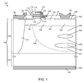
- FIG. 1 is a cross-sectional side view of an example of an n-channel LDMOS device 100 constructed in accordance with an embodiment.
- the device 100 may be configured for operation as an RF LDMOS transistor device.
- the device 100 includes a semiconductor substrate 102 having a first conductivity type, a gate structure 110 supported by a first surface 103 of the semiconductor substrate 102, and source and drain regions 130, 140 (or more generally "current-carrying regions") on either side of the gate structure 110.
- the drain region 140 is laterally separated from the gate structure 110 across the first surface 103, and a drift region 150 of a second (opposite) conductivity type extends laterally from the drain region 140 to the gate structure 110.
- the device 100 also includes one or more buried regions 160, 162 of the second conductivity type disposed in the semiconductor substrate 102 directly below and vertically aligned with the drain region 140, as will be described in more detail below.
- the semiconductor substrate 102 includes a base semiconductor layer 104 and a plurality of epitaxial layers 106.
- the base semiconductor layer 104 may include silicon or another semiconductor material, which is heavily doped with one or more dopants having the first conductivity type to render the base semiconductor layer 104 degenerate (e.g., a doping concentration in a range of about 3x10 18 cm -3 to 2x10 19 cm -3 ), and to provide for conductivity through the base semiconductor layer 104 to a backside contact 180 on a second surface 105 of the substrate 102.
- the dopant concentration for the base semiconductor layer 104 is sufficient to achieve a relatively low substrate resistivity in a range of about 7 ohm-cm to about 11 ohm-cm, although the dopant concentration may be selected to achieve lower or higher resistivity, as well.
- base semiconductor layer 104 may be moderately doped, lightly doped, or undoped.
- the base semiconductor layer 104 may have a silicon-on-insulator (SOI) structure.
- the epitaxial layers 106 also may be doped with dopant(s) of the first conductivity type.
- the epitaxial layers 106 are more lightly doped than the base semiconductor layer 104 (e.g., the epitaxial layers 106 may have a doping concentration in a range of about 1.3x10 15 cm -3 to 1.9x10 15 cm -3 ).
- the semiconductor substrate 102 includes a plurality of moderately doped p-type epitaxial layers 106 (e.g., p or p-) grown on a heavily doped p-type base semiconductor layer 104 (e.g., p+ or p++).
- the base semiconductor layer 104 and the epitaxial layers 106 may be doped with a p-type dopant such as boron (B).
- the device area may include or correspond with one or more active areas of the device 100.
- the device area is defined by one or more doped isolating regions (not shown) in the semiconductor substrate 102 (e.g., in the epitaxial layers 106).
- the doped isolating region(s) may surround the device area. These regions act as a barrier separating the device area from other portions of the substrate 102 (or the base semiconductor layer 104).
- the device area may be further defined via a moderately or heavily doped n-type isolating well laterally surrounding the device area.
- the isolating well may be ring-shaped.
- the device area may alternatively or additionally be defined by one or more isolation regions, such as a shallow trench isolation (STI) region, a deep trench isolation (DTI) region, or a field oxide region (fieldox).
- STI shallow trench isolation
- DTI deep trench isolation
- fieldox field oxide region
- the device 100 includes a well or diffused region 132 in the semiconductor substrate 102.
- a channel or channel region is formed in the well region 132 at a surface 103 of the semiconductor substrate 102.
- the channel is formed under a gate structure 110 of the device 100 via application of a bias voltage to a conductive portion (e.g., polysilicon layer 114) of the gate structure 110.
- the well region 132 may be a region formed by lateral diffusion under the gate structure 110.
- the well region 132 may be considered a body or base region of the device 100.
- the well region 132 has the first conductivity type (e.g., p-type), and is formed in the uppermost epitaxial layer (e.g., epitaxial layer 506, FIG.
- the p-type well region 132 is more heavily doped than the uppermost epitaxial layer (e.g., the well region 132 may have a doping concentration in a range of about 3x10 16 cm -3 to 5x10 17 cm -3 ).
- the well region 132 may be configured to establish a desired threshold voltage and/or other operational parameters of the device 100. For example, the dopant concentration level and the depth of the well region 132 may be configured to set the threshold voltage.
- the gate structure 110 is formed on or above the semiconductor substrate 102 over the well region 132.
- the gate structure 110 includes an oxide or other dielectric layer 112 disposed on the surface 103.
- the dielectric layer 112 may include silicon dioxide (or oxide) deposited or otherwise formed on the surface 103.
- the gate structure 110 may include any number of dielectric layers.
- the dielectric layer spaces a polysilicon or other conductive layer 114 of the gate structure 110 from the well region 132.
- One or more metal interconnect layers 116 may, in turn, be disposed on the polysilicon layer 114.
- the materials, shape, construction, and other characteristics of the gate structure 110 may vary. For example, the lateral extent to which the well region 132 extends under the gate structure 110 may vary from the example shown.
- the gate structure 110 may include additional components.
- the gate structure 110 may include one or more dielectric sidewall spacers disposed along lateral edges 118, 120 of the gate structure 103.
- the sidewall spacers may cover the lateral edges 118, 120 to act as a silicide block to prevent a silicide short along the surface 103.
- the sidewall spacers may provide spacing to separate the conductive components of the gate structure 110 from other structures or components of the device 100.
- One or more of the sidewall spacers may alternatively or additionally be used for alignment purposes in defining an edge of one or more regions of the device 100. The edges of one or more other regions may be aligned with the gate structure 110 as described below.
- the device 100 also includes a heavily doped source region 130 and a drain region 140 of the second conductivity type in the semiconductor substrate 102.
- the source region 130 and drain region 140 may be doped with an n-type dopant such as arsenic (As), phosphorus (P), or antimony (Sb).
- the source region 130 and the drain region 140 are laterally spaced from one another at the surface 103 of the semiconductor substrate 102, and the gate structure 110 is supported by the semiconductor substrate 102 between the source region 130 and the drain region 140.
- the source region 130 may be disposed along or aligned with a first sidewall 120 of the gate structure 110, whereas the drain region 140 is laterally separated across the surface 103 of the substrate 102 from a second, opposite sidewall 118 of the gate structure 110.
- the source region 130 and the drain region 140 may have additional or alternative lateral spacing. Any number of source regions 130 and drain regions 140 may be provided.
- the drain region 140 may be centered or otherwise disposed between, or laterally surrounded by, two portions of the source region 130 or two separate source regions.
- the device 100 may be configured as a single transistor with a dual gate finger configuration.
- the source region 130 and the drain region 140 are n-type doped portions of the uppermost epitaxial layer (e.g., epitaxial layer 506, FIG. 5 ).
- the heavily doped n-type source region 130 is adjacent the well region 132.
- the heavily doped n-type drain region 140 is spaced from the source 130 and the well 132. Such spacing defines a conduction path of the device between the source region 130 and the drain region 140.
- the source region 130 and the drain region 140, or a portion thereof, may have a dopant concentration at a level sufficient to establish ohmic contacts with electrodes or interconnects 136 and 142, for biasing or applying voltages to the source region 130 and the drain region 140, respectively.
- the drain region 140 may be biased or otherwise disposed at a relatively high drain-source voltage (Vds) relative to the source region 130.
- Vds drain-source voltage
- Device 100 also may include a sinker region 134, which extends from the source electrode 136, through the epitaxial layers 106 to the base semiconductor layer 104.
- the sinker region 134 may be configured as a relatively heavily doped region of the first conductivity type (e.g., p-type) to establish an electrical connection between the source electrode 136 (and, thus, the source region 130) and the base semiconductor layer 104.
- the base semiconductor layer 104 is conductive (e.g., heavily doped)
- the sinker region 134 further provides a conductive path to a backside or back surface 105 of the semiconductor substrate 102 on which a backside contact 180 (e.g., formed of metal or other conductive material) is deposited or otherwise disposed.
- the backside contact 180 may form an Ohmic contact with the base semiconductor layer 104 to complete the electrical connection between the source region 130 and the backside contact 180.
- device 100 may include conductive vias ("blind vias") between the top surface 103 of the substrate 102 through epitaxial layers 106 to the base semiconductor substrate 104, where the conductive vias may be electrically connected with the source region 130.
- device 100 may include conductive through substrate vias (TSVs) that extend the entire distance between the top and bottom substrate surfaces 103, 105, and opposite ends of the TSVs may be electrically coupled with the source region 130 and the backside contact 180, respectively.
- TSVs through substrate vias
- charge carriers in some embodiments, electrons; in other embodiments, holes
- charge carriers accumulate in a region at or near the surface 103 under or below the gate structure 110, thereby forming a channel that electrically extends from the source region 130 toward the drain region 140.
- the channel region is located in the well region 132 and other p-type portions of the semiconductor substrate 102 under the gate structure 110.
- the accumulation of charge carriers results in a majority charge carrier inversion in the channel region from the p-type well region 132 (or uppermost epitaxial layer) to an n-type conduction layer or area near the surface 103 of the semiconductor substrate 102.
- charge carriers e.g., electrons
- charge carriers are capable of flowing along a conduction path from the source region 130 to the drain region 140.
- the device 100 also includes a drift region 150 in the semiconductor substrate 102 between the well region 132 and the drain region 140 in accordance with an embodiment.
- the drift region 150 includes a first lateral section 152 adjacent to (e.g., under and/or next to) the drain region 140 and a second lateral section 154 adjacent to (e.g., next to, and either touching or not touching) the well section 132.
- the depth of the lower boundary 155 of the drift region 150 is greater than a depth of the well region 132. In an alternate embodiment, the depth of the lower boundary 155 of the drift region 150 may be less than the depth of the well region 132.
- the drift region 150 is established via the formation of an n-type well.
- the n-type well may be configured for high voltage device operation, and may thus be referred to as an n-type high-voltage (NHV) well.
- the portion of the drift region 150 underlying the drain region 140 may have a dopant concentration lower than the dopant concentration of the source region 130 and the drain region 140 to support high voltage device operation.
- the drift region 150 may support the creation of an accumulation region under the gate structure 110. In this example, the drift region 150 extends up to or under a drain-side portion or sidewall 118 of the gate structure 110.
- the drift region 150 laterally extends from the drain-side sidewall 118 of the gate structure 110 to the drain region 140, which may be formed in or otherwise on the drift region 150.
- the lateral extension of the drift region 150 allows charge carriers (e.g., electrons) in the channel region to reach the drain region 140 during operation.
- the lateral extent of the drift region 150 may vary.
- FIG. 1 illustrates a drift region 150 that abuts the well region 132, in an alternate embodiment, an area of epitaxial layer 106 material may be present between the well region 132 and the drift region 150.
- the depth, size, and other characteristics of the drift region 150 may vary.
- the device 100 may include one or more Faraday or other shield plates 122, 124 disposed along or over a portion of the drift region 150 and a drain-side edge or sidewall 118 of the gate structure 110.
- the device 100 may include one or more passivation layers 170 covering the surface 103.
- the shield plate(s) 122, 124 are disposed between adjacent dielectric or passivation layers 170.
- the shield plate(s) 122, 124 may help protect the dielectric layer 112 of the gate structure 110 from damage or degradation arising from charge carriers accelerated under the electric field arising from the drain-source voltage.
- the shield plate(s) 122, 124 may also help to reduce the maximum electric field in the drift region 150.
- the shield plate(s) 122, 124 may be grounded or otherwise biased to deter injection of such hot carriers into the oxide or other dielectric material under the gate structure 110 and/or the oxide or other dielectric material over the drift region 150.
- the device 100 also includes a shield plate dopant region 156 of the second conductivity type (e.g., n-type) formed in the drift region 150 at a portion of the surface 103 ofthe substrate 102 just below the shield plate(s) 122, 124.
- the shield plate dopant region 156 has a higher dopant concentration than the drift region 150, or more particularly than the second lateral section 154 of the drift region 150.
- the shield plate dopant region 156 may have a doping concentration in a range of about 1x10 16 cm -3 to 9.5x10 16 cm -3 .
- the shield plate dopant region 156 is positioned a gap distance away from the drain-side sidewall 118 of the gate structure 110, which may help to avoid hot carrier injection issues in the device 100.
- the gap distance may be less than half the length of the second lateral section 154 of the drift region 150.
- a width of the shield plate dopant region 156 may be relatively small compared with the length of the second lateral section 154 of the drift region.
- the device 100 also includes one or more buried regions 160, 162 of the second conductivity type underlying the drain region 140.
- the buried regions 160, 162 may have a doping concentration in a range of 1.8x10 15 cm -3 to 2.1x10 15 cm -3 , although the doping concentration may be higher or lower, as well.
- the buried regions 160, 162 may have substantially the same doping concentration, or significantly different doping concentrations from each other.
- a first portion 107 of the semiconductor substrate 102 with the first conductivity type is present between the lowest buried region 160 and the base semiconductor layer 104
- a second portion 108 of the semiconductor substrate 102 with the first conductivity type is present between buried regions 160, 162
- a third portion 109 of the semiconductor substrate 102 with the first conductivity type is present between the uppermost buried region 162 and the drain region 140 (or the first lateral section 152 of the drift region 150).
- the lowest buried region 160 has a width that is greater than a width of the uppermost buried region 162.
- the buried regions 160, 162 may have substantially the same width, or the uppermost buried region 162 may be wider than the lowest buried region 160.
- Buried regions 160, 162 may be electrically floating structures, in an embodiment, meaning that buried regions 160, 162 essentially are electrically isolated from other current carrying structures or regions.
- either or both of buried regions 160, 162 may be contacted by a conductive via or by a sinker region of the second conductivity type, which electrically couples the buried region(s) 160, 162 with the top surface 103 of the substrate 102.
- a bias voltage may be applied to the buried region(s) 160, 162 to actively alter their influence on the operation of device 100.
- the buried regions 160, 162 help to stretch the depletion line (e.g., indicated by line 190) deeper into the semiconductor substrate 102 than may be achieved using a similarly-constructed device that lacks buried regions 160, 162.
- device 100 may have a relatively low drain-to-gate capacitance (Cdg) and drain-to-source capacitance (Cds), when compared with such a device, as well as a relatively high source-to-drain breakdown voltage (BVdss) and relatively low on-state drain-to-source resistance (Rdson).
- Cdg drain-to-gate capacitance
- Cds drain-to-source capacitance
- BVdss source-to-drain breakdown voltage
- Rdson on-state drain-to-source resistance
- device 100 is shown to include two buried regions 160, 162, alternate embodiments may include a single buried region, multiple merged buried regions, or more than two distinct buried regions.
- the device 100 is shown in simplified form in FIG. 1 .
- FIG. 1 does not depict a number of metal layers configured for electric connections with the source region 130, the drain region 140, and the gate structure 110.
- the device 100 may have a number of other structures or components for connectivity, isolation, passivation, and other purposes not shown in FIG. 1 for ease in illustration.
- the device 100 may include any number of isolating regions or layers. Any number of STI regions, DTI regions or fieldox regions may be formed at the surface 103 of the semiconductor substrate 102. Other STI regions may be disposed in the semiconductor substrate 102 within the active device area to isolate or separate various contact regions.
- the device 100 may be configured with one or more lightly or intermediately doped transition regions (e.g., n-type lightly doped drain, or NLDD, regions) at or near the source region 130 and the drain region 140.
- Each transition region may be or include a diffused region formed in connection with the source region 130 and/or the drain region 140 and may thus be referred to herein as a source/drain extension region.
- Such transition regions may assist in controlling the electric field at or near the surface 103, including in areas other than those areas near the source region 130 or the drain region 140.
- the dopant concentrations, thicknesses, and other characteristics of the above-described semiconductor regions in the semiconductor substrate 102 may vary.
- the dopant concentration of the base semiconductor layer 104 may vary considerably.
- the dopant concentrations and/or depths may have values larger or smaller than the values or ranges provided herein.
- FIG. 2 is a flowchart of a method of fabricating a semiconductor device (e.g., device 100) in accordance with an embodiment.
- FIG. 2 should be viewed in conjunction with FIGs 3-6 , which are cross-sectional side views of the device of FIG. 1 during various fabrication stages in accordance with an embodiment.
- the transistor device is fabricated with a semiconductor substrate, the regions or layers of which may have the conductivity types of the n-channel example described above, or a device alternatively may be configured to support a p-channel device.
- the method includes a sequence of acts, only the salient of which are depicted for convenience in illustration. It is to be understood that the relative ordering of some acts shown in the flowchart of FIG.
- the method may begin, in block 202 by forming (or "growing") a p-type epitaxial layer 306 on a p-type base semiconductor layer 104.
- the p-type base semiconductor layer 104 may constitute a portion of a semiconductor wafer with an initial thickness of about 500 microns, although the initial thickness of the base semiconductor layer 104 may be thicker or thinner, as well.
- the base semiconductor layer 104 may include heavily doped p-type semiconductor material (e.g., silicon or another semiconductor material), in an embodiment. In alternate embodiments, the base semiconductor layer 104 may be moderately doped, lightly doped, or un-doped, or may have an SOI or other substrate structure.
- the epitaxial layer 306 may be grown to a thickness 308 in a range of about 5 microns to about 20 microns (e.g., about 13 microns), although the epitaxial layer 306 may be thicker or thinner, as well.
- the epitaxial layer 306 may be moderately or lightly doped p-type in-situ, in an embodiment.
- the epitaxial layer 306 may be deposited un-doped, and may thereafter be doped with a p-type dopant to a desired dopant concentration.
- Blocks 204, 206, and 208 represent a process for forming one or more buried regions (e.g., regions 160, 162). Although block 204 may be performed just a single time to form a single buried region (and blocks 206 and 208 may be excluded), one or more iterations of the sequence of blocks 204, 206, and 208 may be performed to form multiple buried regions, as well. The below description corresponds to performing two iterations of the buried region formation processes, resulting in the formation of two buried regions. As indicated above, in alternate embodiments, only one iteration of block 204 may be performed to form one buried region, or more than two iterations of blocks 204, 206, 208 may be performed to form more than two buried regions.
- a first doped region 160 is formed, according to an embodiment. Although it is not buried at this stage, the first doped region 160 will be referred to as a first "buried" region (or lowest buried region) hereafter for consistency with the rest of the description, and because the first doped region 160 ultimately will be buried under additional epitaxially formed semiconductor material.
- n-type dopant ions 310 are implanted into a portion of the surface of the epitaxial layer 306 that ultimately will align in the vertical direction with a later-formed drain region (e.g., drain region 140, FIG. 1 ). This results in an n-type buried region 160 at the surface of the epitaxial layer 306.
- the dopant ions 310 are implanted so that the first buried region 160 has a dopant concentration in a range of about 1.8x10 15 cm -3 to about 2.1x10 15 cm -3 , and the dopant ions 310 are implanted using an ion energy in a range of about 500 kilo-electron volts (KeV) to about 800 KeV.
- the dopant concentration and/or ion energy may be lower or higher than the above given ranges.
- the first buried region 160 prior to or after further diffusion into the semiconductor substrate 102, has a width 362 in a range of about 1.0 microns to about 7.0 microns, where the width 362 depends on the drift length of the to-be-formed drift region 150 (i.e., the distance from sidewall 118 of the gate structure 110 to the gate-side edge of the to-be-formed drain region 140).
- the width 362 of the first buried region 160 may be determined by a RESURF (REduced SURFace field) charge balance requirement for a particular device voltage rating (e.g., a higher voltage rating may warrant a longer drift length, and thus a relatively-wider width 362).
- RESURF REduced SURFace field
- the first buried region 160 has a thickness 364 in a range of about 0.5 microns to about 1.0 microns after initial implantation.
- the final thickness 364 of the first buried region 160 i.e., after all thermal processes have been completed in conjunction with forming the device 100
- the first buried region 160 may be wider or narrower and/or thicker or thinner, in other embodiments.
- the thickness 364 of the first buried region 160 is less than the thickness 308 of the epitaxial layer 306, in an embodiment, resulting in a first portion 107 of p-type semiconductor material underlying the first buried region 160 (i.e., between the first buried region 160 and the base substrate layer 104).
- the distance between the lower extent of the first buried region 160 and the base substrate layer 104 is in a range of about 30 microns to about 60 microns.
- a thermal process e.g., an annealing step
- the thermal process also may result in diffusion of the n-type dopant from the first buried region 160 into surrounding portions of the first epitaxial layer 306, as indicated by the altered shape of buried region 160 in subsequent figures.
- one or more additional buried regions may be formed, as indicated by decision block 206.
- a second buried region e.g., region 162
- a second (or next) p-type epitaxial layer 406 is formed on the first epitaxial layer 306 in block 208.
- the second epitaxial layer 406 may be thinner than the first epitaxial layer 306.
- the second epitaxial layer 406 may be grown to a thickness 408 in a range of about 3 microns to about 6 microns (e.g., about 4 microns), although the epitaxial layer 406 may be thicker or thinner, as well.
- the epitaxial layer 406 may be moderately or lightly doped p-type in-situ, in an embodiment.
- the epitaxial layer 406 may be deposited un-doped, and may thereafter be doped with a p-type dopant to a desired dopant concentration.
- a second doped region 162 (or upper buried region) is formed, according to an embodiment.
- a portion of the top surface of the epitaxial layer 406 is masked (mask not illustrated), and n-type dopant ions 410 are implanted into a portion of the surface of the epitaxial layer 406 that aligns with the first doped region 160 in the vertical direction, and that also will ultimately align in the vertical direction with a later-formed drain region (e.g., drain region 140, FIG. 1 ). This results in an n-type buried region 162 at the surface of the epitaxial layer 406.
- the dopant ions 410 are implanted so that the second buried region 162 has a dopant concentration in a range of about 1.8x10 15 cm -3 to about 2.1x10 15 cm -3 , and the dopant ions 410 are implanted using an ion energy in a range of about 500 KeV to about 800 KeV.
- the dopant concentration and/or ion energy may be lower or higher than the above given ranges.
- the second buried region 162 prior to or after further diffusion into the semiconductor substrate 102, has a width 462 in a range of about 1.0 microns to about 5 microns, where the width 462 also depends on the drift length of the to-be-formed drift region 150, and may be determined by a RESURF charge balance requirement for a particular device voltage rating.
- the second buried region 162 has a thickness 464 in a range of about 0.5 microns to about 1.0 microns after initial implantation.
- the final thickness 464 of the first buried region 160 i.e., after all thermal processes have been completed
- the second buried region 162 may be wider or narrower and/or thicker or thinner, in other embodiments. As the above-given ranges indicate, the second buried region 162 may be narrower (in the horizontal direction) and thinner (in the vertical direction) than the first buried region 160. Alternatively, the first and second buried regions 160, 162 may have substantially similar dimensions, or the second buried region 162 may be wider and/or thicker than the first buried region 160. In any event, the depth 464 of the second buried region 162 is less than the thickness 408 of the epitaxial layer 406, in an embodiment, resulting in a second portion 108 of p-type semiconductor material underlying the second buried region 162 (i.e., between the first and second buried regions 160, 162).
- the distance between the lower extent of the second buried region 162 and the upper extent of the first buried region 160 is in a range of about 3 microns to about 5 microns.
- a thermal process e.g., an annealing step
- the thermal process also may result in diffusion of the n-type dopant from the second buried region 162 into surrounding portions of the second epitaxial layer 406, and further diffusion of the n-type dopant from the first buried region 160 into surrounding portions of the first and second epitaxial layers 306, 406, as indicated by the altered shapes of buried regions 160, 162 in subsequent figures.
- buried regions 160, 162 are shown to be distinct regions (i.e., with p-type semiconductor material 108 between them), the implantation and thermal processes of block 204 may be carried out so that buried regions 160, 162 merge together, in an alternate embodiment.
- one or more additional (top) p-type epitaxial layers 506 are formed on the second epitaxial layer 406.
- the top epitaxial layer 506 may be grown to a thickness 508 in a range of about 4 microns to about 8 microns (e.g., about 6 microns), although the epitaxial layer 506 may be thicker or thinner, as well.
- the epitaxial layer 506 may be moderately or lightly doped p-type in-situ, in an embodiment.
- the epitaxial layer 506 may be deposited un-doped, and may thereafter be doped with a p-type dopant to a desired dopant concentration.
- the top surface of epitaxial layer 506 corresponds to the top surface 103 of substrate 102.
- a device may include three epitaxial layers 306, 406, 506, those of skill in the art would understand, based on the description herein, that the number of epitaxial layers 306, 406, 506 is not limited to three. In general, the number of epitaxial layers is directly related to the desired BV dss (e.g., the higher the BV dss is, the more epitaxial layers may be included).
- the gate structure 110 and various doped regions 132, 134, 140, 150, 156 extending into the semiconductor substrate 102 from the top surface 103 of the semiconductor substrate 102 are formed.
- formation of the gate structure 110 and the various doped regions 132, 134, 140, 150, 156 are described in a particular order below, the gate structure 110 and the doped regions 132, 134, 140, 150, 156 may be formed in different orders, as well.
- Standard semiconductor processing techniques may be used to form the gate structure 110 and the various doped regions 132, 134, 140, 150, 156, and the details of those standard techniques are not discussed in detail herein.
- the gate structure 110 is formed by sequentially forming a dielectric layer 112, a polysilicon layer 114, and a metal interconnect layer 116 on the top surface 103 of the semiconductor substrate 102, and performing a patterned etching process to define the gate structure 110.
- Semiconductor devices with a conductive gate electrode positioned over a dielectric or other insulator may be considered MOS devices despite the lack of a metal gate electrode and an oxide gate insulator.
- MOS metal-oxide-semiconductor and the abbreviation "MOS” may be used even though such devices may not employ metals or oxides but various combinations of conductive materials (e.g., metals, alloys, silicides, doped semiconductors, etc., instead of simple metals, and insulating materials other than oxides). Accordingly, as used herein, the terms MOS and LDMOS are intended to include such variations.
- sinker region 134 the top semiconductor surface 103 is masked (mask not illustrated) with an opening corresponding to the sinker region location.
- a p-type dopant (not illustrated) is then implanted in the semiconductor surface 103, where the implant process is configured to extend the sinker region 134 through all of the epitaxial layers 106 to reach the base semiconductor layer 104.
- the sinker region 134 may be formed during the epitaxial layer formation processes.
- the sinker region 134 has a dopant concentration in a range of about 1x10 19 cm -3 to about 3x10 19 cm -3 , although the dopant concentration may be larger or smaller, as well.
- the top semiconductor surface 103 again may be masked (mask not illustrated) with an opening at the source-side sidewall 120 of the gate structure 110, and a p-type dopant (not illustrated) is implanted into the semiconductor surface 103 through the opening.
- a drive procedure may then be performed to allow the well region 132 to extend a desired lateral distance under the gate structure 110 via lateral diffusion.
- the well region 132 may be implanted into the semiconductor substrate 102 prior to formation of the gate structure 110.
- the well region 132 has a depth in a range of about 0.6 microns to about 1.2 microns, and a dopant concentration in a range of about 3x10 16 cm -3 to about 5x10 17 cm -3 , although the dopant concentration may be larger or smaller, as well.
- the drift region 150 may be formed using one or multiple masking and implantation processes, which result in a drift region 150 with a desired thickness and shape, in an embodiment.
- the top semiconductor surface 103 may be masked (mask not illustrated) with an opening at the drain-side sidewall 118 of the gate structure 110, and an n-type dopant is implanted into the semiconductor surface 103 through the opening.
- the drain-side sidewall 118 of the gate structure 110 may be used to align the drift region 150 with the gate structure 110, in an embodiment.
- a drive procedure may be performed to achieve a desired depth and dopant concentration profile for the drift region 150.
- the drift region 150 has a depth in a range of about 0.6 microns to about 3 microns, and a dopant concentration in a range of about 2.3x10 15 cm -3 to about 9x10 16 cm 3 , although the dopant concentration may be larger or smaller, as well.
- the thickness 652 of the drift region 150 is less than the thickness 508 of the epitaxial layer 506, in an embodiment, resulting in a third portion 109 of p-type semiconductor material underlying the drift region 150 (i.e., between the drift region 150 and the second buried region 162).
- the distance between the lower extent of the drift region 150 and the upper extent of the second buried region 162 is in a range of about 5 microns to about 8 microns, and the distance between the drain region 140 and the upper extent of the second buried region 162 is in a range of about 8 microns to about 12 microns.
- These distances may depend, for example, on the device voltage rating.
- the above-given ranges may be appropriate for devices with voltage ratings in a range of about 28 volts (V) to about 80 V with a BV dss in a range of about 70 V to about 250 V.
- the voltage ratings may be higher or lower, and accordingly, the distance between the lower extent of the drift region 150 and the upper extent of the second buried region 162 (and/or the distance between the drain region 140 and the upper extend of the second buried region 162) may be greater or smaller than the above-given range.
- One or more additional n-type implant processes are performed to form source, drain, and shield plate dopant regions 130, 140, 156.
- a mask layer (not illustrated) and the source-side sidewall 120 of the gate structure 110 may be used as a mask to align the source region 130 with the gate structure 110.
- One or more additional masks (not illustrated) may be used to define the locations of the drain and shield plate dopant regions 140, 156, and an n-type dopant 610 is implanted into the semiconductor surface 103 through the openings in the mask layer(s).
- One or more drive procedures may be used to achieve desired depths and dopant concentration profiles for the source, drain, and shield plate dopant regions 130, 140, 156.
- the source and drain dopant regions 130, 140 each has a depth in a range of about 0.2 microns to about 0.26 microns, and a dopant concentration in a range of about 1.0x10 20 cm -3 to about 2.0x10 20 cm -3
- the shield plate dopant region 156 has a depth in a range of about 0.2 microns to about 0.26 microns, and a dopant concentration in a range of about 1x10 16 cm -3 to about 9.5x10 16 cm -3 .
- the depths and dopant concentrations of the source, drain, and shield plate dopant regions 130, 140, 156 may be larger or smaller than the above-given ranges, as well.
- a set of one or more shield plates e.g., shield plates 122 and/or 124, and shield plate dielectric 170 are formed.
- forming the set of shield plates 122, 124 includes forming a first dielectric layer of the shield plate dielectric 170 over the gate 110 and portions of the substrate surface 103, forming a lower shield plate 122 over the first dielectric layer, forming a second dielectric layer of the shield plate dielectric 170 over the lower shield plate 122, and forming an upper shield plate 124 over the second dielectric layer.
- shield plate materials include, but are not limited to, doped polysilicon, metal-silicide including a tungsten silicide (e.g., WSi), a metal such as aluminum or copper, an alloy, or any other material or combination of materials that exhibits a desirable electrical conductivity.
- An additional dielectric layer may be formed over the upper shield plate 124, and the dielectric structure may be patterned and etched to complete the shield plate dielectric 170 with embedded shield plates 122, 124.
- At least one of the shield plates 122, 124 has a portion that overlies the shield plate dopant region 156.
- the upper shield plate 124 has an end that extends closer to the drain dopant region 140 than an end of the lower shield plate 122. Consequently, the upper shield plate 124 overlies or extends over a first portion of the drift dopant region 150 that is longer in length than a second portion of the drift dopant region 150 over which the lower shield plate 122 extends.
- the upper 124 and lower 122 shield plates are physically and electrically isolated from each other with a layer of the shield plate dielectric 170.
- conductive contacts 136, 142 are formed.
- contact 136 is formed on the surface 103 to electrically connect to the source dopant region 130 and to the sinker region 134
- contact 142 is formed on the surface 103 to electrically connect to the drain dopant region 140.
- Various additional dielectric layers (not illustrated) and metal layers (not illustrated) are thereafter formed to complete the frontside of the device 100.
- the backside of the substrate 102 is thinned (e.g., using a backgrinding process) and backside contact 180 is formed on the back surface 105.
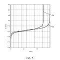
- FIG. 7 shows a plot of drain-source current versus drain-source voltage illustrating breakdown voltages for (a) trace 902: a device that lacks buried regions (e.g., buried regions 160, 162) in the substrate underlying the drain region, and (b) trace 904: a device that includes buried regions (e.g., buried regions 160, 162) in the substrate underlying the drain region, in accordance with an embodiment.
- trace 902 a device that lacks buried regions (e.g., buried regions 160, 162) in the substrate underlying the drain region
- trace 904 a device that includes buried regions (e.g., buried regions 160, 162) in the substrate underlying the drain region, in accordance with an embodiment.
- a device that includes one or more buried regions underlying the drain region in accordance with an embodiment may have a substantially higher breakdown voltage than a device that lacks such buried region(s).
- An embodiment of a semiconductor device includes a semiconductor substrate having a first conductivity type, a first surface, and an opposed second surface, a gate structure supported by the first surface of the semiconductor substrate, and a first current carrying region disposed in the semiconductor substrate at the first surface.
- the first current carrying region is laterally separated from the gate structure.
- the device further includes a drift region of a second conductivity type disposed in the semiconductor substrate at the first surface, where the second conductivity type is opposite the first conductivity type, and the drift region extends laterally from the first current carrying region to the gate structure.
- the device further includes a first buried region of the second conductivity type disposed in the semiconductor substrate below the first current carrying region. The first buried region is vertically aligned with the first current carrying region, and a first portion of the semiconductor substrate with the first conductivity type is present between the first buried region and the first current carrying region.
- the first buried region is electrically floating.
- the semiconductor device further comprises a conductive structure that electrically couples the first buried region with the first surface of the semiconductor substrate.
- the conductive structure is selected from a conductive via and a sinker region of the second conductivity type.
- the semiconductor substrate comprises a base semiconductor layer, a first epitaxial layer in which the first buried region is deposited, and a second epitaxial layer over the first epitaxial layer, wherein a surface of the second epitaxial layer corresponds to the first surface of the semiconductor substrate.
- a distance between the first current carrying region and an upper extent of the first buried region is in a range of 8 microns to 12 microns.
- the semiconductor device further comprises a second buried region of the second conductivity type disposed in the semiconductor substrate below the first buried region.
- the second buried region is vertically aligned with the first buried region and the first current carrying region.
- a second portion of the semiconductor substrate with the first conductivity type is present between the first and second buried regions.
- a thickness of the second portion of the semiconductor substrate between the first and second buried regions is in a range of 3 microns to 5 microns.
- the semiconductor substrate comprises a base semiconductor layer, a first epitaxial layer in which the first buried region is deposited, a second epitaxial layer over the first epitaxial layer and in which the second buried region is deposited, and a third epitaxial layer over the second epitaxial layer.
- a surface of the third epitaxial layer corresponds to the first surface of the semiconductor substrate.
- the first epitaxial layer has a thickness in a range of 9 microns to 13 microns
- the second epitaxial layer has a thickness in a range of 3 microns to 5 microns
- the third epitaxial layer has a thickness in a range of 3 microns to 5 microns.
- the semiconductor device further comprises one or more additional buried regions of the second conductivity type disposed in the semiconductor substrate directly below the first and second buried regions.
- Each of the first, second, and additional buried regions are separated by portions of the semiconductor substrate with the first conductivity type.
- a semiconductor device includes a substrate and a field-effect transistor device disposed in the substrate.
- the field-effect transistor device includes a semiconductor substrate having a first conductivity type, a first surface, and an opposed second surface, a gate structure supported by the first surface of the semiconductor substrate, and a drain region disposed in the semiconductor substrate at the first surface. The drain region is laterally separated from the gate structure.
- the field-effect transistor device further includes a drift region of a second conductivity type disposed in the semiconductor substrate at the first surface, where the second conductivity type is opposite the first conductivity type, and the drift region extends laterally from the drain region to a first edge of the gate structure.
- the field-effect transistor device further includes a first buried region of the second conductivity type disposed in the semiconductor substrate below the drain region.
- the first buried region is vertically aligned with the first drain region, and a first portion of the semiconductor substrate with the first conductivity type is present between the first buried region and the drain region.
- the semiconductor substrate comprises a base semiconductor layer, a first epitaxial layer in which the first buried region is deposited, and a second epitaxial layer over the first epitaxial layer.
- a surface of the second epitaxial layer corresponds to the first surface of the semiconductor substrate.
- the first epitaxial layer has a thickness in a range of 5 microns to 20 microns
- the second epitaxial layer has a thickness in a range of 4 microns to 8 microns.
- the semiconductor device further comprises a second buried region of the second conductivity type disposed in the semiconductor substrate below the first buried region, wherein the second buried region is vertically aligned with the first buried region and the drain region. A second portion of the semiconductor substrate with the first conductivity type is present between the first buried region and the second buried region.
- the semiconductor substrate comprises a base semiconductor layer, a first epitaxial layer in which the first buried region is deposited, a second epitaxial layer over the first epitaxial layer and in which the second buried region is deposited, and a third epitaxial layer over the second epitaxial layer.
- a surface of the third epitaxial layer corresponds to the first surface of the semiconductor substrate.
- the first epitaxial layer has a thickness in a range of 5 microns to 20 microns
- the second epitaxial layer has a thickness in a range of 3 microns to 6 microns
- the third epitaxial layer has a thickness in a range of 4 microns to 8 microns.
- An embodiment of a method of fabricating a semiconductor device includes forming a first epitaxial layer of a first conductivity type over a base semiconductor layer, and forming a first buried region in the first epitaxial layer, where the first buried region has a second conductivity type that is opposite the first conductivity type.
- the method further includes forming a second epitaxial layer of the first conductivity type over the first epitaxial layer, where a surface of the second epitaxial layer corresponds to a first surface of a semiconductor substrate.
- the method further includes forming a gate structure over the first surface of the semiconductor substrate, forming a source region and a drain region in the second epitaxial layer, and forming a drift region of the second conductivity type in the semiconductor substrate.
- the drift region extends laterally from the drain region to the gate structure, a first portion of the second epitaxial layer with the first conductivity type is present between the first buried region and the drift region, and the first buried region is vertically aligned with the drift region.
- the forming the first buried region comprises masking at least a portion of the first epitaxial layer; implanting a dopant having the second conductivity type in at least an unmasked portion of the first epitaxial layer, at least a portion of the unmasked portion being vertically aligned with the drain region; performing a thermal process; and forming the second epitaxial layer over the first epitaxial layer.
- the method further comprises forming a third epitaxial layer of the first conductivity type between the base semiconductor layer and the first epitaxial layer; and forming a second buried region in the third epitaxial layer.
- the second buried region has the second conductivity type, a first portion of the first epitaxial layer with the first conductivity type is present between the first buried region and the second buried region, and the second buried region is vertically aligned with the first buried region and the drift region.
- the method further comprises forming a well region in the semiconductor substrate below the gate structure.
- the well region is configured to form a channel between the source region and the drift region during operation of the semiconductor device.
Landscapes
- Insulated Gate Type Field-Effect Transistor (AREA)
Abstract
Description
- Embodiments relate generally to semiconductor devices, and more specifically to lateral semiconductor devices, such as laterally diffused metal oxide semiconductor (LDMOS) field effect transistors (FETs).
- Integrated circuits (ICs) and other electronic devices often include arrangements of interconnected field-effect transistors (FETs), also called metal-oxide-semiconductor field-effect transistors (MOSFETs), or simply MOS transistors or devices. A typical MOS transistor includes a gate electrode and spaced-apart source and drain electrodes. A control voltage applied to the gate electrode controls the flow of current through a variably conductive channel between the source and drain electrodes.
- Power transistor devices are designed to be tolerant of the high currents and voltages that are present in some applications. Some power transistor devices are also designed to handle radio frequency (RF) signals, such as the devices used in wireless communications and other RF power amplifier applications. One type of RF power transistor device is a laterally diffused metal-oxide-semiconductor (LDMOS) transistor. In an LDMOS device, charge carriers drift through a drift space between a channel region and the drain electrode under the electric field arising from an operating voltage applied between the source and drain electrodes.
- The output power density and linear efficiency of an RF LDMOS transistor is affected by the transistor's drain-source capacitance, (Cds), drain-gate capacitance (Cdg), on-state drain-to-source resistance (Rdson), and source-to-drain breakdown voltage (BVdss). Generally, there is a desire in the industry to develop RF LDMOS transistors with higher power densities and improved linear efficiencies. Accordingly, there is a desire in the industry to develop RF LDMOS transistors with lower Cds, Cdg, and Rdson, and higher BVdss.
- A more complete understanding of the subject matter may be derived by referring to the detailed description and claims when considered in conjunction with the following figures, wherein like reference numbers refer to similar elements throughout the figures.
-
FIG. 1 is a cross-sectional side view of an exemplary semiconductor device in accordance with an embodiment. -
FIG. 2 is a flowchart of a method of fabricating a semiconductor device in accordance with an embodiment. -
FIGs 3-6 are cross-sectional side views of the device ofFIG. 1 during various fabrication stages in accordance with an embodiment. -
FIG. 7 is a plot of drain-source current versus drain-source voltage for devices with and without buried regions in the substrate underlying the drain region. - An embodiment of an LDMOS transistor includes a substrate having a first conductivity type, and at least one buried region having a second conductivity type in a portion of the substrate that is below and vertically aligned with a drain region of the transistor. During device operation, the buried region(s) help to stretch the depletion line deeper into the semiconductor substrate than may be achieved using a conventional device that lacks the aforementioned buried region(s). Because drain-to-gate capacitance (Cdg) and drain-to-source capacitance (Cds) are inversely proportional to depletion depth, LDMOS devices with such buried region(s) may have a relatively low drain-to-gate capacitance (Cdg) and drain-to-source capacitance (Cds), when compared with conventional devices. In addition, LDMOS devices with such buried region(s) also may have a relatively high source-to-drain breakdown voltage (BVdss) and relatively low on-state drain-to-source resistance (Rdson), when compared with conventional devices.
- According to a further embodiment, an LDMOS device also may have a relatively deep high voltage region of a conductivity type opposite the substrate conductivity type (e.g., an n-type or NHV region) buried under the drain contact and extending towards the gate. For example, in an embodiment, a deep high voltage region is merged with a shallow high voltage region in order to form a drift region. The relatively deep, composite high voltage region may enable a conventional scaling plateau between BVdss and drift length to be broken, resulting in a higher BVdss while keeping Rdson relatively low, when compared with conventional devices that lack such a high voltage region.
- According to another further embodiment, an LDMOS device may have an additional high density implant in the NHV drift region below a gate shield plate. This additional implant, referred to herein as a "shield plate dopant region," may increase the charge density in the drift region, thus improving drift region resistance and reducing Rdson. Not only is the implant potentially helpful in reducing Rdson, but the implant also may be effective in increasing BVdss.
- Throughout this description and in the appended claims, the term "buried" as used in reference to a dopant and/or a doped region refers to the dopant or at least a portion of the doped region being present at a depth below a semiconductor substrate surface that is greater than a depth achievable via standard ion implantation. As used herein, the phrase "standard ion implantation" refers to conventional methods known in the industry as of the filing date of this patent application. In some embodiments, the term "buried" describes a depth greater than about 1 micron beneath a top surface of a semiconductor substrate. In some embodiments, the depth is greater than about 3.0 microns, in some embodiments greater than about 6.0 microns, in some embodiments greater than about 9.0 microns, in some embodiments greater than about 12.0 microns, and in some embodiments greater than about 15.0 microns.
- Although described below in connection with n-channel LDMOS transistors, the disclosed devices are not limited to any particular transistor configuration. N-channel LDMOS devices are described and illustrated herein for convenience of description and without any intended limitation. The device embodiments are not limited to n-channel devices, as p-channel and other types of devices may be provided by, for example, substitution of semiconductor regions of opposite conductivity type. Thus, for example, each semiconductor region, layer or other structure in the examples described below may have a conductivity type (e.g., n-type or p-type) opposite to the type identified in the examples below.
-
FIG. 1 is a cross-sectional side view of an example of an n-channel LDMOS device 100 constructed in accordance with an embodiment. Thedevice 100 may be configured for operation as an RF LDMOS transistor device. Thedevice 100 includes asemiconductor substrate 102 having a first conductivity type, agate structure 110 supported by afirst surface 103 of thesemiconductor substrate 102, and source anddrain regions 130, 140 (or more generally "current-carrying regions") on either side of thegate structure 110. Thedrain region 140 is laterally separated from thegate structure 110 across thefirst surface 103, and adrift region 150 of a second (opposite) conductivity type extends laterally from thedrain region 140 to thegate structure 110. According to an embodiment, thedevice 100 also includes one or more buriedregions semiconductor substrate 102 directly below and vertically aligned with thedrain region 140, as will be described in more detail below. - The
semiconductor substrate 102 includes abase semiconductor layer 104 and a plurality ofepitaxial layers 106. Thebase semiconductor layer 104 may include silicon or another semiconductor material, which is heavily doped with one or more dopants having the first conductivity type to render thebase semiconductor layer 104 degenerate (e.g., a doping concentration in a range of about 3x1018cm-3 to 2x1019cm-3), and to provide for conductivity through thebase semiconductor layer 104 to abackside contact 180 on asecond surface 105 of thesubstrate 102. According to an embodiment, the dopant concentration for thebase semiconductor layer 104 is sufficient to achieve a relatively low substrate resistivity in a range of about 7 ohm-cm to about 11 ohm-cm, although the dopant concentration may be selected to achieve lower or higher resistivity, as well. In alternate embodiments,base semiconductor layer 104 may be moderately doped, lightly doped, or undoped. In still another alternate embodiment, thebase semiconductor layer 104 may have a silicon-on-insulator (SOI) structure. - The
epitaxial layers 106 also may be doped with dopant(s) of the first conductivity type. For example, theepitaxial layers 106 are more lightly doped than the base semiconductor layer 104 (e.g., theepitaxial layers 106 may have a doping concentration in a range of about 1.3x1015cm-3 to 1.9x1015cm-3). According to a specific embodiment, thesemiconductor substrate 102 includes a plurality of moderately doped p-type epitaxial layers 106 (e.g., p or p-) grown on a heavily doped p-type base semiconductor layer 104 (e.g., p+ or p++). In such an embodiment, thebase semiconductor layer 104 and theepitaxial layers 106 may be doped with a p-type dopant such as boron (B). - A device area is depicted in
FIG. 1 . The device area may include or correspond with one or more active areas of thedevice 100. In some embodiments, the device area is defined by one or more doped isolating regions (not shown) in the semiconductor substrate 102 (e.g., in the epitaxial layers 106). The doped isolating region(s) may surround the device area. These regions act as a barrier separating the device area from other portions of the substrate 102 (or the base semiconductor layer 104). For example, the device area may be further defined via a moderately or heavily doped n-type isolating well laterally surrounding the device area. The isolating well may be ring-shaped. The device area may alternatively or additionally be defined by one or more isolation regions, such as a shallow trench isolation (STI) region, a deep trench isolation (DTI) region, or a field oxide region (fieldox). - The
device 100 includes a well or diffusedregion 132 in thesemiconductor substrate 102. During operation, a channel or channel region is formed in thewell region 132 at asurface 103 of thesemiconductor substrate 102. The channel is formed under agate structure 110 of thedevice 100 via application of a bias voltage to a conductive portion (e.g., polysilicon layer 114) of thegate structure 110. Thewell region 132 may be a region formed by lateral diffusion under thegate structure 110. Thewell region 132 may be considered a body or base region of thedevice 100. In this example, thewell region 132 has the first conductivity type (e.g., p-type), and is formed in the uppermost epitaxial layer (e.g.,epitaxial layer 506,FIG. 5 ) of thesemiconductor substrate 102. The p-type well region 132 is more heavily doped than the uppermost epitaxial layer (e.g., thewell region 132 may have a doping concentration in a range of about 3x1016cm-3 to 5x1017cm-3). Thewell region 132 may be configured to establish a desired threshold voltage and/or other operational parameters of thedevice 100. For example, the dopant concentration level and the depth of thewell region 132 may be configured to set the threshold voltage. - The
gate structure 110 is formed on or above thesemiconductor substrate 102 over thewell region 132. Thegate structure 110 includes an oxide or otherdielectric layer 112 disposed on thesurface 103. For example, thedielectric layer 112 may include silicon dioxide (or oxide) deposited or otherwise formed on thesurface 103. Thegate structure 110 may include any number of dielectric layers. The dielectric layer spaces a polysilicon or otherconductive layer 114 of thegate structure 110 from thewell region 132. One or more metal interconnect layers 116 may, in turn, be disposed on thepolysilicon layer 114. The materials, shape, construction, and other characteristics of thegate structure 110 may vary. For example, the lateral extent to which thewell region 132 extends under thegate structure 110 may vary from the example shown. Thegate structure 110 may include additional components. For example, thegate structure 110 may include one or more dielectric sidewall spacers disposed alonglateral edges gate structure 103. The sidewall spacers may cover thelateral edges surface 103. Further, the sidewall spacers may provide spacing to separate the conductive components of thegate structure 110 from other structures or components of thedevice 100. One or more of the sidewall spacers may alternatively or additionally be used for alignment purposes in defining an edge of one or more regions of thedevice 100. The edges of one or more other regions may be aligned with thegate structure 110 as described below. - The
device 100 also includes a heavily dopedsource region 130 and adrain region 140 of the second conductivity type in thesemiconductor substrate 102. For example, in an embodiment, thesource region 130 and drainregion 140 may be doped with an n-type dopant such as arsenic (As), phosphorus (P), or antimony (Sb). Thesource region 130 and thedrain region 140 are laterally spaced from one another at thesurface 103 of thesemiconductor substrate 102, and thegate structure 110 is supported by thesemiconductor substrate 102 between thesource region 130 and thedrain region 140. Thesource region 130 may be disposed along or aligned with afirst sidewall 120 of thegate structure 110, whereas thedrain region 140 is laterally separated across thesurface 103 of thesubstrate 102 from a second,opposite sidewall 118 of thegate structure 110. In some embodiments, thesource region 130 and thedrain region 140 may have additional or alternative lateral spacing. Any number ofsource regions 130 anddrain regions 140 may be provided. For example, thedrain region 140 may be centered or otherwise disposed between, or laterally surrounded by, two portions of thesource region 130 or two separate source regions. For example, thedevice 100 may be configured as a single transistor with a dual gate finger configuration. In this example, thesource region 130 and thedrain region 140 are n-type doped portions of the uppermost epitaxial layer (e.g.,epitaxial layer 506,FIG. 5 ). The heavily doped n-type source region 130 is adjacent thewell region 132. The heavily doped n-type drain region 140 is spaced from thesource 130 and thewell 132. Such spacing defines a conduction path of the device between thesource region 130 and thedrain region 140. Thesource region 130 and thedrain region 140, or a portion thereof, may have a dopant concentration at a level sufficient to establish ohmic contacts with electrodes or interconnects 136 and 142, for biasing or applying voltages to thesource region 130 and thedrain region 140, respectively. During operation, thedrain region 140 may be biased or otherwise disposed at a relatively high drain-source voltage (Vds) relative to thesource region 130. -
Device 100 also may include asinker region 134, which extends from thesource electrode 136, through theepitaxial layers 106 to thebase semiconductor layer 104. Thesinker region 134 may be configured as a relatively heavily doped region of the first conductivity type (e.g., p-type) to establish an electrical connection between the source electrode 136 (and, thus, the source region 130) and thebase semiconductor layer 104. In an embodiment in which thebase semiconductor layer 104 is conductive (e.g., heavily doped), thesinker region 134 further provides a conductive path to a backside or backsurface 105 of thesemiconductor substrate 102 on which a backside contact 180 (e.g., formed of metal or other conductive material) is deposited or otherwise disposed. Thebackside contact 180 may form an Ohmic contact with thebase semiconductor layer 104 to complete the electrical connection between thesource region 130 and thebackside contact 180. In an alternate embodiment, rather than relying onsinker region 134 to provide a conductive path from thesource electrode 136 to thebase semiconductor layer 104,device 100 may include conductive vias ("blind vias") between thetop surface 103 of thesubstrate 102 throughepitaxial layers 106 to thebase semiconductor substrate 104, where the conductive vias may be electrically connected with thesource region 130. In still another alternate embodiment,device 100 may include conductive through substrate vias (TSVs) that extend the entire distance between the top and bottom substrate surfaces 103, 105, and opposite ends of the TSVs may be electrically coupled with thesource region 130 and thebackside contact 180, respectively. - When the
gate structure 110 is biased, charge carriers (in some embodiments, electrons; in other embodiments, holes) accumulate in a region at or near thesurface 103 under or below thegate structure 110, thereby forming a channel that electrically extends from thesource region 130 toward thedrain region 140. The channel region is located in thewell region 132 and other p-type portions of thesemiconductor substrate 102 under thegate structure 110. The accumulation of charge carriers (e.g., electrons) results in a majority charge carrier inversion in the channel region from the p-type well region 132 (or uppermost epitaxial layer) to an n-type conduction layer or area near thesurface 103 of thesemiconductor substrate 102. Once a sufficient amount of the charge carriers (e.g., electrons) accumulate in the channel region, charge carriers (e.g., electrons) are capable of flowing along a conduction path from thesource region 130 to thedrain region 140. - The
device 100 also includes adrift region 150 in thesemiconductor substrate 102 between thewell region 132 and thedrain region 140 in accordance with an embodiment. Thedrift region 150 includes a firstlateral section 152 adjacent to (e.g., under and/or next to) thedrain region 140 and a secondlateral section 154 adjacent to (e.g., next to, and either touching or not touching) thewell section 132. In the illustrated embodiment, the depth of thelower boundary 155 of thedrift region 150 is greater than a depth of thewell region 132. In an alternate embodiment, the depth of thelower boundary 155 of thedrift region 150 may be less than the depth of thewell region 132. - According to an embodiment, the
drift region 150 is established via the formation of an n-type well. The n-type well may be configured for high voltage device operation, and may thus be referred to as an n-type high-voltage (NHV) well. For example, the portion of thedrift region 150 underlying thedrain region 140 may have a dopant concentration lower than the dopant concentration of thesource region 130 and thedrain region 140 to support high voltage device operation. Thedrift region 150 may support the creation of an accumulation region under thegate structure 110. In this example, thedrift region 150 extends up to or under a drain-side portion orsidewall 118 of thegate structure 110. Thedrift region 150 laterally extends from the drain-side sidewall 118 of thegate structure 110 to thedrain region 140, which may be formed in or otherwise on thedrift region 150. The lateral extension of thedrift region 150 allows charge carriers (e.g., electrons) in the channel region to reach thedrain region 140 during operation. The lateral extent of thedrift region 150 may vary. For example, althoughFIG. 1 illustrates adrift region 150 that abuts thewell region 132, in an alternate embodiment, an area ofepitaxial layer 106 material may be present between thewell region 132 and thedrift region 150. The depth, size, and other characteristics of thedrift region 150 may vary. - The
device 100 may include one or more Faraday orother shield plates drift region 150 and a drain-side edge orsidewall 118 of thegate structure 110. Thedevice 100 may include one ormore passivation layers 170 covering thesurface 103. In some embodiments, the shield plate(s) 122, 124 are disposed between adjacent dielectric or passivation layers 170. The shield plate(s) 122, 124 may help protect thedielectric layer 112 of thegate structure 110 from damage or degradation arising from charge carriers accelerated under the electric field arising from the drain-source voltage. The shield plate(s) 122, 124 may also help to reduce the maximum electric field in thedrift region 150. The shield plate(s) 122, 124 may be grounded or otherwise biased to deter injection of such hot carriers into the oxide or other dielectric material under thegate structure 110 and/or the oxide or other dielectric material over thedrift region 150. - According to an embodiment, the
device 100 also includes a shieldplate dopant region 156 of the second conductivity type (e.g., n-type) formed in thedrift region 150 at a portion of thesurface 103ofthe substrate 102 just below the shield plate(s) 122, 124. The shieldplate dopant region 156 has a higher dopant concentration than thedrift region 150, or more particularly than the secondlateral section 154 of thedrift region 150. For example, the shieldplate dopant region 156 may have a doping concentration in a range of about 1x1016cm-3 to 9.5x1016cm-3. - According to an embodiment, the shield
plate dopant region 156 is positioned a gap distance away from the drain-side sidewall 118 of thegate structure 110, which may help to avoid hot carrier injection issues in thedevice 100. For example, the gap distance may be less than half the length of the secondlateral section 154 of thedrift region 150. Further, a width of the shieldplate dopant region 156 may be relatively small compared with the length of the secondlateral section 154 of the drift region. - As discussed above, the
device 100 also includes one or more buriedregions drain region 140. For example, the buriedregions regions first portion 107 of thesemiconductor substrate 102 with the first conductivity type is present between the lowest buriedregion 160 and thebase semiconductor layer 104, asecond portion 108 of thesemiconductor substrate 102 with the first conductivity type is present between buriedregions third portion 109 of thesemiconductor substrate 102 with the first conductivity type is present between the uppermostburied region 162 and the drain region 140 (or the firstlateral section 152 of the drift region 150). InFIG. 1 , the lowest buriedregion 160 has a width that is greater than a width of the uppermost buriedregion 162. In alternate embodiments, the buriedregions region 162 may be wider than the lowest buriedregion 160. -
Buried regions regions regions top surface 103 of thesubstrate 102. In such embodiments, a bias voltage may be applied to the buried region(s) 160, 162 to actively alter their influence on the operation ofdevice 100. - During device operation, the buried
regions semiconductor substrate 102 than may be achieved using a similarly-constructed device that lacks buriedregions device 100 may have a relatively low drain-to-gate capacitance (Cdg) and drain-to-source capacitance (Cds), when compared with such a device, as well as a relatively high source-to-drain breakdown voltage (BVdss) and relatively low on-state drain-to-source resistance (Rdson). - Along with a detailed description of an embodiment of a method for forming buried
regions regions FIGs 3-6 . Althoughdevice 100 is shown to include two buriedregions - The
device 100 is shown in simplified form inFIG. 1 . For example,FIG. 1 does not depict a number of metal layers configured for electric connections with thesource region 130, thedrain region 140, and thegate structure 110. Thedevice 100 may have a number of other structures or components for connectivity, isolation, passivation, and other purposes not shown inFIG. 1 for ease in illustration. For instance, thedevice 100 may include any number of isolating regions or layers. Any number of STI regions, DTI regions or fieldox regions may be formed at thesurface 103 of thesemiconductor substrate 102. Other STI regions may be disposed in thesemiconductor substrate 102 within the active device area to isolate or separate various contact regions. - The
device 100 may be configured with one or more lightly or intermediately doped transition regions (e.g., n-type lightly doped drain, or NLDD, regions) at or near thesource region 130 and thedrain region 140. Each transition region may be or include a diffused region formed in connection with thesource region 130 and/or thedrain region 140 and may thus be referred to herein as a source/drain extension region. Such transition regions may assist in controlling the electric field at or near thesurface 103, including in areas other than those areas near thesource region 130 or thedrain region 140. - The dopant concentrations, thicknesses, and other characteristics of the above-described semiconductor regions in the
semiconductor substrate 102 may vary. For example, the dopant concentration of thebase semiconductor layer 104 may vary considerably. The dopant concentrations and/or depths may have values larger or smaller than the values or ranges provided herein. -
FIG. 2 is a flowchart of a method of fabricating a semiconductor device (e.g., device 100) in accordance with an embodiment.FIG. 2 should be viewed in conjunction withFIGs 3-6 , which are cross-sectional side views of the device ofFIG. 1 during various fabrication stages in accordance with an embodiment. The transistor device is fabricated with a semiconductor substrate, the regions or layers of which may have the conductivity types of the n-channel example described above, or a device alternatively may be configured to support a p-channel device. The method includes a sequence of acts, only the salient of which are depicted for convenience in illustration. It is to be understood that the relative ordering of some acts shown in the flowchart ofFIG. 2 is meant to be merely representative rather than limiting, and that alternative sequences may be followed. Moreover, it is likewise to be understood that additional, different, or fewer acts may be provided, and that two or more of these acts may occur sequentially, substantially contemporaneously, and/or in alternative orders. The fabrication method is not limited to any particular doping mechanism, and may include future developed doping techniques. - Referring to both
FIG. 2 and3 , the method may begin, inblock 202 by forming (or "growing") a p-type epitaxial layer 306 on a p-typebase semiconductor layer 104. For example, the p-typebase semiconductor layer 104 may constitute a portion of a semiconductor wafer with an initial thickness of about 500 microns, although the initial thickness of thebase semiconductor layer 104 may be thicker or thinner, as well. As discussed previously, thebase semiconductor layer 104 may include heavily doped p-type semiconductor material (e.g., silicon or another semiconductor material), in an embodiment. In alternate embodiments, thebase semiconductor layer 104 may be moderately doped, lightly doped, or un-doped, or may have an SOI or other substrate structure. - According to an embodiment, the
epitaxial layer 306 may be grown to athickness 308 in a range of about 5 microns to about 20 microns (e.g., about 13 microns), although theepitaxial layer 306 may be thicker or thinner, as well. Theepitaxial layer 306 may be moderately or lightly doped p-type in-situ, in an embodiment. In an alternate embodiment, theepitaxial layer 306 may be deposited un-doped, and may thereafter be doped with a p-type dopant to a desired dopant concentration. -
Blocks regions 160, 162). Althoughblock 204 may be performed just a single time to form a single buried region (and blocks 206 and 208 may be excluded), one or more iterations of the sequence ofblocks block 204 may be performed to form one buried region, or more than two iterations ofblocks - In a first iteration of
block 204, and still referring toFIG. 3 , a firstdoped region 160 is formed, according to an embodiment. Although it is not buried at this stage, the firstdoped region 160 will be referred to as a first "buried" region (or lowest buried region) hereafter for consistency with the rest of the description, and because the firstdoped region 160 ultimately will be buried under additional epitaxially formed semiconductor material. To form the firstburied region 160, a portion of the top surface of theepitaxial layer 306 is masked (mask not illustrated), and n-type dopant ions 310 are implanted into a portion of the surface of theepitaxial layer 306 that ultimately will align in the vertical direction with a later-formed drain region (e.g., drainregion 140,FIG. 1 ). This results in an n-type buriedregion 160 at the surface of theepitaxial layer 306. According to an embodiment, thedopant ions 310 are implanted so that the firstburied region 160 has a dopant concentration in a range of about 1.8x1015cm-3 to about 2.1x1015cm-3, and thedopant ions 310 are implanted using an ion energy in a range of about 500 kilo-electron volts (KeV) to about 800 KeV. In other embodiments, the dopant concentration and/or ion energy may be lower or higher than the above given ranges. - According to an embodiment, prior to or after further diffusion into the
semiconductor substrate 102, the firstburied region 160 has awidth 362 in a range of about 1.0 microns to about 7.0 microns, where thewidth 362 depends on the drift length of the to-be-formed drift region 150 (i.e., the distance fromsidewall 118 of thegate structure 110 to the gate-side edge of the to-be-formed drain region 140). For example, thewidth 362 of the firstburied region 160 may be determined by a RESURF (REduced SURFace field) charge balance requirement for a particular device voltage rating (e.g., a higher voltage rating may warrant a longer drift length, and thus a relatively-wider width 362). According to an embodiment, the firstburied region 160 has athickness 364 in a range of about 0.5 microns to about 1.0 microns after initial implantation. However, thefinal thickness 364 of the first buried region 160 (i.e., after all thermal processes have been completed in conjunction with forming the device 100) may be in a range of about 1.5 microns to about 2.0 microns. The firstburied region 160 may be wider or narrower and/or thicker or thinner, in other embodiments. In any event, thethickness 364 of the firstburied region 160 is less than thethickness 308 of theepitaxial layer 306, in an embodiment, resulting in afirst portion 107 of p-type semiconductor material underlying the first buried region 160 (i.e., between the firstburied region 160 and the base substrate layer 104). According to an embodiment, the distance between the lower extent of the firstburied region 160 and thebase substrate layer 104 is in a range of about 30 microns to about 60 microns. A thermal process (e.g., an annealing step) may be performed after the implantation ofblock 204 in order to prepare the surface of the firstburied region 160 for growth of additional epitaxial material above it. The thermal process also may result in diffusion of the n-type dopant from the firstburied region 160 into surrounding portions of thefirst epitaxial layer 306, as indicated by the altered shape of buriedregion 160 in subsequent figures. - After formation of the first
buried region 160, one or more additional buried regions may be formed, as indicated bydecision block 206. For example, and referring now toFIG. 4 , to form a second buried region (e.g., region 162) over the firstburied region 160, a second (or next) p-type epitaxial layer 406 is formed on thefirst epitaxial layer 306 inblock 208. According to an embodiment, thesecond epitaxial layer 406 may be thinner than thefirst epitaxial layer 306. For example, thesecond epitaxial layer 406 may be grown to athickness 408 in a range of about 3 microns to about 6 microns (e.g., about 4 microns), although theepitaxial layer 406 may be thicker or thinner, as well. Once again, theepitaxial layer 406 may be moderately or lightly doped p-type in-situ, in an embodiment. In an alternate embodiment, theepitaxial layer 406 may be deposited un-doped, and may thereafter be doped with a p-type dopant to a desired dopant concentration. - In a second iteration of
block 204, and still referring toFIG. 4 , a second doped region 162 (or upper buried region) is formed, according to an embodiment. To form the secondburied region 162, a portion of the top surface of theepitaxial layer 406 is masked (mask not illustrated), and n-type dopant ions 410 are implanted into a portion of the surface of theepitaxial layer 406 that aligns with the firstdoped region 160 in the vertical direction, and that also will ultimately align in the vertical direction with a later-formed drain region (e.g., drainregion 140,FIG. 1 ). This results in an n-type buriedregion 162 at the surface of theepitaxial layer 406. According to an embodiment, thedopant ions 410 are implanted so that the secondburied region 162 has a dopant concentration in a range of about 1.8x1015cm-3 to about 2.1x1015cm-3, and thedopant ions 410 are implanted using an ion energy in a range of about 500 KeV to about 800 KeV. In other embodiments, the dopant concentration and/or ion energy may be lower or higher than the above given ranges. - According to an embodiment, prior to or after further diffusion into the
semiconductor substrate 102, the secondburied region 162 has awidth 462 in a range of about 1.0 microns to about 5 microns, where thewidth 462 also depends on the drift length of the to-be-formed drift region 150, and may be determined by a RESURF charge balance requirement for a particular device voltage rating. According to an embodiment, the secondburied region 162 has athickness 464 in a range of about 0.5 microns to about 1.0 microns after initial implantation. However, thefinal thickness 464 of the first buried region 160 (i.e., after all thermal processes have been completed) may be in a range of about 1.0 microns to about 1.5 microns. The secondburied region 162 may be wider or narrower and/or thicker or thinner, in other embodiments. As the above-given ranges indicate, the secondburied region 162 may be narrower (in the horizontal direction) and thinner (in the vertical direction) than the firstburied region 160. Alternatively, the first and second buriedregions buried region 162 may be wider and/or thicker than the firstburied region 160. In any event, thedepth 464 of the secondburied region 162 is less than thethickness 408 of theepitaxial layer 406, in an embodiment, resulting in asecond portion 108 of p-type semiconductor material underlying the second buried region 162 (i.e., between the first and second buriedregions 160, 162). According to an embodiment, the distance between the lower extent of the secondburied region 162 and the upper extent of the firstburied region 160 is in a range of about 3 microns to about 5 microns. A thermal process (e.g., an annealing step) may be performed after the implantation ofblock 204 in order to prepare the surface of the secondburied region 162 for growth of additional epitaxial material above it. The thermal process also may result in diffusion of the n-type dopant from the secondburied region 162 into surrounding portions of thesecond epitaxial layer 406, and further diffusion of the n-type dopant from the firstburied region 160 into surrounding portions of the first and secondepitaxial layers regions regions type semiconductor material 108 between them), the implantation and thermal processes ofblock 204 may be carried out so that buriedregions - In
block 210, and referring toFIG. 5 , one or more additional (top) p-type epitaxial layers 506 (referred to in the singular, below) are formed on thesecond epitaxial layer 406. According to an embodiment, thetop epitaxial layer 506 may be grown to athickness 508 in a range of about 4 microns to about 8 microns (e.g., about 6 microns), although theepitaxial layer 506 may be thicker or thinner, as well. Once again, theepitaxial layer 506 may be moderately or lightly doped p-type in-situ, in an embodiment. In an alternate embodiment, theepitaxial layer 506 may be deposited un-doped, and may thereafter be doped with a p-type dopant to a desired dopant concentration. The top surface ofepitaxial layer 506 corresponds to thetop surface 103 ofsubstrate 102. Although the above description indicates that a device may include threeepitaxial layers epitaxial layers - Referring now to
FIG. 6 and block 212, thegate structure 110 and variousdoped regions semiconductor substrate 102 from thetop surface 103 of thesemiconductor substrate 102 are formed. Although formation of thegate structure 110 and the variousdoped regions gate structure 110 and the dopedregions gate structure 110 and the variousdoped regions - The
gate structure 110 is formed by sequentially forming adielectric layer 112, apolysilicon layer 114, and ametal interconnect layer 116 on thetop surface 103 of thesemiconductor substrate 102, and performing a patterned etching process to define thegate structure 110. Semiconductor devices with a conductive gate electrode positioned over a dielectric or other insulator may be considered MOS devices despite the lack of a metal gate electrode and an oxide gate insulator. Commonly, the terms metal-oxide-semiconductor and the abbreviation "MOS" may be used even though such devices may not employ metals or oxides but various combinations of conductive materials (e.g., metals, alloys, silicides, doped semiconductors, etc., instead of simple metals, and insulating materials other than oxides). Accordingly, as used herein, the terms MOS and LDMOS are intended to include such variations. - To form
sinker region 134, thetop semiconductor surface 103 is masked (mask not illustrated) with an opening corresponding to the sinker region location. A p-type dopant (not illustrated) is then implanted in thesemiconductor surface 103, where the implant process is configured to extend thesinker region 134 through all of theepitaxial layers 106 to reach thebase semiconductor layer 104. In an alternate embodiment, thesinker region 134 may be formed during the epitaxial layer formation processes. According to an embodiment, thesinker region 134 has a dopant concentration in a range of about 1x1019cm-3 to about 3x1019cm-3, although the dopant concentration may be larger or smaller, as well. - To form the
well region 132, thetop semiconductor surface 103 again may be masked (mask not illustrated) with an opening at the source-side sidewall 120 of thegate structure 110, and a p-type dopant (not illustrated) is implanted into thesemiconductor surface 103 through the opening. A drive procedure may then be performed to allow thewell region 132 to extend a desired lateral distance under thegate structure 110 via lateral diffusion. In an alternate embodiment, thewell region 132 may be implanted into thesemiconductor substrate 102 prior to formation of thegate structure 110. According to an embodiment, thewell region 132 has a depth in a range of about 0.6 microns to about 1.2 microns, and a dopant concentration in a range of about 3x1016cm-3 to about 5x1017cm-3, although the dopant concentration may be larger or smaller, as well. - The
drift region 150 may be formed using one or multiple masking and implantation processes, which result in adrift region 150 with a desired thickness and shape, in an embodiment. Again, thetop semiconductor surface 103 may be masked (mask not illustrated) with an opening at the drain-side sidewall 118 of thegate structure 110, and an n-type dopant is implanted into thesemiconductor surface 103 through the opening. The drain-side sidewall 118 of thegate structure 110 may be used to align thedrift region 150 with thegate structure 110, in an embodiment. In addition, a drive procedure may be performed to achieve a desired depth and dopant concentration profile for thedrift region 150. According to an embodiment, thedrift region 150 has a depth in a range of about 0.6 microns to about 3 microns, and a dopant concentration in a range of about 2.3x1015cm-3 to about 9x1016cm3, although the dopant concentration may be larger or smaller, as well. According to an embodiment, thethickness 652 of thedrift region 150 is less than thethickness 508 of theepitaxial layer 506, in an embodiment, resulting in athird portion 109 of p-type semiconductor material underlying the drift region 150 (i.e., between thedrift region 150 and the second buried region 162). According to an embodiment, the distance between the lower extent of thedrift region 150 and the upper extent of the secondburied region 162 is in a range of about 5 microns to about 8 microns, and the distance between thedrain region 140 and the upper extent of the secondburied region 162 is in a range of about 8 microns to about 12 microns. These distances may depend, for example, on the device voltage rating. For example, the above-given ranges may be appropriate for devices with voltage ratings in a range of about 28 volts (V) to about 80 V with a BVdss in a range of about 70 V to about 250 V. In other embodiments, the voltage ratings may be higher or lower, and accordingly, the distance between the lower extent of thedrift region 150 and the upper extent of the second buried region 162 (and/or the distance between thedrain region 140 and the upper extend of the second buried region 162) may be greater or smaller than the above-given range. - One or more additional n-type implant processes are performed to form source, drain, and shield
plate dopant regions side sidewall 120 of thegate structure 110 may be used as a mask to align thesource region 130 with thegate structure 110. One or more additional masks (not illustrated) may be used to define the locations of the drain and shieldplate dopant regions type dopant 610 is implanted into thesemiconductor surface 103 through the openings in the mask layer(s). One or more drive procedures may be used to achieve desired depths and dopant concentration profiles for the source, drain, and shieldplate dopant regions dopant regions plate dopant region 156 has a depth in a range of about 0.2 microns to about 0.26 microns, and a dopant concentration in a range of about 1x1016cm-3 to about 9.5x1016cm-3. The depths and dopant concentrations of the source, drain, and shieldplate dopant regions - Referring again to
FIG. 1 and block 214, a set of one or more shield plates, e.g.,shield plates 122 and/or 124, andshield plate dielectric 170 are formed. In an embodiment, forming the set ofshield plates gate 110 and portions of thesubstrate surface 103, forming alower shield plate 122 over the first dielectric layer, forming a second dielectric layer of the shield plate dielectric 170 over thelower shield plate 122, and forming anupper shield plate 124 over the second dielectric layer. Some example shield plate materials include, but are not limited to, doped polysilicon, metal-silicide including a tungsten silicide (e.g., WSi), a metal such as aluminum or copper, an alloy, or any other material or combination of materials that exhibits a desirable electrical conductivity. An additional dielectric layer may be formed over theupper shield plate 124, and the dielectric structure may be patterned and etched to complete the shield plate dielectric 170 with embeddedshield plates - According to an embodiment, at least one of the
shield plates plate dopant region 156. In the embodiment shown, theupper shield plate 124 has an end that extends closer to thedrain dopant region 140 than an end of thelower shield plate 122. Consequently, theupper shield plate 124 overlies or extends over a first portion of thedrift dopant region 150 that is longer in length than a second portion of thedrift dopant region 150 over which thelower shield plate 122 extends. Additionally, the upper 124 and lower 122 shield plates are physically and electrically isolated from each other with a layer of theshield plate dielectric 170. Although twoshield plates FIG. 1 , a device may include only a single shield plate or more than two shield plates, in other embodiments. - In
block 216,conductive contacts surface 103 to electrically connect to thesource dopant region 130 and to thesinker region 134, and contact 142 is formed on thesurface 103 to electrically connect to thedrain dopant region 140. Various additional dielectric layers (not illustrated) and metal layers (not illustrated) are thereafter formed to complete the frontside of thedevice 100. In addition, the backside of thesubstrate 102 is thinned (e.g., using a backgrinding process) andbackside contact 180 is formed on theback surface 105. -
FIG. 7 shows a plot of drain-source current versus drain-source voltage illustrating breakdown voltages for (a) trace 902: a device that lacks buried regions (e.g., buriedregions 160, 162) in the substrate underlying the drain region, and (b) trace 904: a device that includes buried regions (e.g., buriedregions 160, 162) in the substrate underlying the drain region, in accordance with an embodiment. As shown inFIG. 7 , a device that includes one or more buried regions underlying the drain region in accordance with an embodiment may have a substantially higher breakdown voltage than a device that lacks such buried region(s). - An embodiment of a semiconductor device includes a semiconductor substrate having a first conductivity type, a first surface, and an opposed second surface, a gate structure supported by the first surface of the semiconductor substrate, and a first current carrying region disposed in the semiconductor substrate at the first surface. The first current carrying region is laterally separated from the gate structure. The device further includes a drift region of a second conductivity type disposed in the semiconductor substrate at the first surface, where the second conductivity type is opposite the first conductivity type, and the drift region extends laterally from the first current carrying region to the gate structure. The device further includes a first buried region of the second conductivity type disposed in the semiconductor substrate below the first current carrying region. The first buried region is vertically aligned with the first current carrying region, and a first portion of the semiconductor substrate with the first conductivity type is present between the first buried region and the first current carrying region.
- In an example, the first buried region is electrically floating.
- In an example, the semiconductor device further comprises a conductive structure that electrically couples the first buried region with the first surface of the semiconductor substrate. The conductive structure is selected from a conductive via and a sinker region of the second conductivity type.
- In an example, the semiconductor substrate comprises a base semiconductor layer, a first epitaxial layer in which the first buried region is deposited, and a second epitaxial layer over the first epitaxial layer, wherein a surface of the second epitaxial layer corresponds to the first surface of the semiconductor substrate.
- In an example, a distance between the first current carrying region and an upper extent of the first buried region is in a range of 8 microns to 12 microns.
- In an example, the semiconductor device further comprises a second buried region of the second conductivity type disposed in the semiconductor substrate below the first buried region. The second buried region is vertically aligned with the first buried region and the first current carrying region. A second portion of the semiconductor substrate with the first conductivity type is present between the first and second buried regions.
- The semiconductor device of
claim 6, wherein a thickness of the second portion of the semiconductor substrate between the first and second buried regions is in a range of 3 microns to 5 microns. - In an example, the semiconductor substrate comprises a base semiconductor layer, a first epitaxial layer in which the first buried region is deposited, a second epitaxial layer over the first epitaxial layer and in which the second buried region is deposited, and a third epitaxial layer over the second epitaxial layer. A surface of the third epitaxial layer corresponds to the first surface of the semiconductor substrate.
- In an example, the first epitaxial layer has a thickness in a range of 9 microns to 13 microns, the second epitaxial layer has a thickness in a range of 3 microns to 5 microns, and the third epitaxial layer has a thickness in a range of 3 microns to 5 microns.
- In an example, the semiconductor device further comprises one or more additional buried regions of the second conductivity type disposed in the semiconductor substrate directly below the first and second buried regions. Each of the first, second, and additional buried regions are separated by portions of the semiconductor substrate with the first conductivity type.
- Another embodiment of a semiconductor device includes a substrate and a field-effect transistor device disposed in the substrate. The field-effect transistor device includes a semiconductor substrate having a first conductivity type, a first surface, and an opposed second surface, a gate structure supported by the first surface of the semiconductor substrate, and a drain region disposed in the semiconductor substrate at the first surface. The drain region is laterally separated from the gate structure. The field-effect transistor device further includes a drift region of a second conductivity type disposed in the semiconductor substrate at the first surface, where the second conductivity type is opposite the first conductivity type, and the drift region extends laterally from the drain region to a first edge of the gate structure. The field-effect transistor device further includes a first buried region of the second conductivity type disposed in the semiconductor substrate below the drain region. The first buried region is vertically aligned with the first drain region, and a first portion of the semiconductor substrate with the first conductivity type is present between the first buried region and the drain region.
- In an example, the semiconductor substrate comprises a base semiconductor layer, a first epitaxial layer in which the first buried region is deposited, and a second epitaxial layer over the first epitaxial layer. A surface of the second epitaxial layer corresponds to the first surface of the semiconductor substrate.
- In an example, the first epitaxial layer has a thickness in a range of 5 microns to 20 microns, and the second epitaxial layer has a thickness in a range of 4 microns to 8 microns.
- In an example, the semiconductor device further comprises a second buried region of the second conductivity type disposed in the semiconductor substrate below the first buried region, wherein the second buried region is vertically aligned with the first buried region and the drain region. A second portion of the semiconductor substrate with the first conductivity type is present between the first buried region and the second buried region.
- In an example, the semiconductor substrate comprises a base semiconductor layer, a first epitaxial layer in which the first buried region is deposited, a second epitaxial layer over the first epitaxial layer and in which the second buried region is deposited, and a third epitaxial layer over the second epitaxial layer. A surface of the third epitaxial layer corresponds to the first surface of the semiconductor substrate.
- In an example, the first epitaxial layer has a thickness in a range of 5 microns to 20 microns, the second epitaxial layer has a thickness in a range of 3 microns to 6 microns, and the third epitaxial layer has a thickness in a range of 4 microns to 8 microns.
- An embodiment of a method of fabricating a semiconductor device includes forming a first epitaxial layer of a first conductivity type over a base semiconductor layer, and forming a first buried region in the first epitaxial layer, where the first buried region has a second conductivity type that is opposite the first conductivity type. The method further includes forming a second epitaxial layer of the first conductivity type over the first epitaxial layer, where a surface of the second epitaxial layer corresponds to a first surface of a semiconductor substrate. The method further includes forming a gate structure over the first surface of the semiconductor substrate, forming a source region and a drain region in the second epitaxial layer, and forming a drift region of the second conductivity type in the semiconductor substrate. The drift region extends laterally from the drain region to the gate structure, a first portion of the second epitaxial layer with the first conductivity type is present between the first buried region and the drift region, and the first buried region is vertically aligned with the drift region.
- In an example, the forming the first buried region comprises masking at least a portion of the first epitaxial layer; implanting a dopant having the second conductivity type in at least an unmasked portion of the first epitaxial layer, at least a portion of the unmasked portion being vertically aligned with the drain region; performing a thermal process; and forming the second epitaxial layer over the first epitaxial layer.
- In an example, the method further comprises forming a third epitaxial layer of the first conductivity type between the base semiconductor layer and the first epitaxial layer; and forming a second buried region in the third epitaxial layer. The second buried region has the second conductivity type, a first portion of the first epitaxial layer with the first conductivity type is present between the first buried region and the second buried region, and the second buried region is vertically aligned with the first buried region and the drift region.
- In an example, the method further comprises forming a well region in the semiconductor substrate below the gate structure. The well region is configured to form a channel between the source region and the drift region during operation of the semiconductor device.
- The preceding detailed description is merely illustrative in nature and is not intended to limit the embodiments of the subject matter or the application and uses of such embodiments. As used herein, the word "exemplary" means "serving as an example, instance, or illustration." Any implementation described herein as exemplary is not necessarily to be construed as preferred or advantageous over other implementations. Furthermore, there is no intention to be bound by any expressed or implied theory presented in the preceding technical field, background, or detailed description.
- The connecting lines shown in the various figures contained herein are intended to represent exemplary functional relationships and/or physical couplings between the various elements. It should be noted that many alternative or additional functional relationships or physical connections may be present in an embodiment of the subject matter. In addition, certain terminology may also be used herein for the purpose of reference only, and thus are not intended to be limiting, and the terms "first", "second" and other such numerical terms referring to structures do not imply a sequence or order unless clearly indicated by the context.
- The foregoing description refers to elements or nodes or features being "connected" or "coupled" together. As used herein, unless expressly stated otherwise, "connected" means that one element is directly joined to (or directly communicates with) another element, and not necessarily mechanically. Likewise, unless expressly stated otherwise, "coupled" means that one element is directly or indirectly joined to (or directly or indirectly communicates with, electrically or otherwise) another element, and not necessarily mechanically. Thus, although the schematic shown in the figures depict one exemplary arrangement of elements, additional intervening elements, devices, features, or components may be present in an embodiment of the depicted subject matter.
- While at least one exemplary embodiment has been presented in the foregoing detailed description, it should be appreciated that a vast number of variations exist. It should also be appreciated that the exemplary embodiment or embodiments described herein are not intended to limit the scope, applicability, or configuration of the claimed subject matter in any way. Rather, the foregoing detailed description will provide those skilled in the art with a convenient road map for implementing the described embodiment or embodiments. It should be understood that various changes can be made in the function and arrangement of elements without departing from the scope defined by the claims, which includes known equivalents and foreseeable equivalents at the time of filing this patent application.
Claims (15)
- A semiconductor device comprising:a semiconductor substrate (102) having a first conductivity type, a first surface (103), and an opposed second surface;a gate structure (110) supported by the first surface of the semiconductor substrate;a first current carrying region (130, 140) disposed in the semiconductor substrate at the first surface, wherein the first current carrying region is laterally separated from the gate structure;a drift region (150) of a second conductivity type disposed in the semiconductor substrate at the first surface, wherein the second conductivity type is opposite the first conductivity type, and the drift region extends laterally from the first current carrying region to the gate structure; anda first buried region (160) of the second conductivity type disposed in the semiconductor substrate below the first current carrying region, wherein the first buried region is vertically aligned with the first current carrying region, and a first portion (107) of the semiconductor substrate with the first conductivity type is present between the first buried region and the first current carrying region.
- The semiconductor device of claim 1,wherein the first buried region is electrically floating.
- The semiconductor device of claim 1 or claim 2, further comprising:a conductive structure that electrically couples the first buried region with the first surface of the semiconductor substrate, wherein the conductive structure is selected from a conductive via and a sinker region (134) of the second conductivity type.
- The semiconductor device of any preceding claim,wherein a distance between the first current carrying region and an upper extent of the first buried region is in a range of 8 microns to 12 microns.
- The semiconductor device of any preceding claim,wherein the semiconductor substrate comprises a base semiconductor layer (104), a first epitaxial layer (306) in which the first buried region is deposited, and a second epitaxial layer (406) over the first epitaxial layer, wherein a surface of the second epitaxial layer corresponds to the first surface of the semiconductor substrate.
- The semiconductor device of claim 5,wherein the first epitaxial layer has a thickness in a range of 5 microns to 20 microns, and the second epitaxial layer has a thickness in a range of 4 microns to 8 microns.
- The semiconductor device of any one of the claims 1 to 4, further comprising:a second buried region (162) of the second conductivity type disposed in the semiconductor substrate below the first buried region, wherein the second buried region is vertically aligned with the first buried region and the first current carrying region, and a second portion (108) of the semiconductor substrate with the first conductivity type is present between the first and second buried regions.
- The semiconductor device of claim 7,wherein the semiconductor substrate comprises a base semiconductor layer (104), a first epitaxial layer (306) in which the first buried region is deposited, a second epitaxial layer (406) over the first epitaxial layer and in which the second buried region is deposited, and a third epitaxial layer (506) over the second epitaxial layer, wherein a surface of the third epitaxial layer corresponds to the first surface of the semiconductor substrate.
- The semiconductor device of claim 8,wherein the first epitaxial layer has a thickness in a range of 5 microns to 20 microns, the second epitaxial layer has a thickness in a range of 3 microns to 6 microns, and the third epitaxial layer has a thickness in a range of 4 microns to 8 microns.
- The semiconductor device of claim 7 to 9, further comprising:one or more additional buried regions of the second conductivity type disposed in the semiconductor substrate directly below the first and second buried regions, wherein each of the first, second, and additional buried regions are separated by portions of the semiconductor substrate with the first conductivity type.
- A semiconductor device comprising:a substrate; anda field-effect transistor device disposed in the substrate, wherein the field-effect transistor device is a semiconductor device (100) according to any one of the claims 1 to 10, wherein the first current carrying region is a drain region (140).
- A method of fabricating a semiconductor device, the method comprising:forming (202) a first epitaxial layer (306) of a first conductivity type over a base semiconductor layer (104);forming (204) a first buried region (160) in the first epitaxial layer, wherein the first buried region has a second conductivity type that is opposite the first conductivity type;forming (210) a second epitaxial layer (406) of the first conductivity type over the first epitaxial layer, wherein a surface of the second epitaxial layer corresponds to a first surface of a semiconductor substrate;forming (212) a gate structure (110) over the first surface of the semiconductor substrate;forming (212) a source region (130) and a drain region (140) in the second epitaxial layer; andforming (212) a drift region (150) of the second conductivity type in the semiconductor substrate, the drift region extending laterally from the drain region to the gate structure, wherein a first portion (107) of the second epitaxial layer with the first conductivity type is present between the first buried region and the drift region, and the first buried region is vertically aligned with the drift region.
- The method of claim 12, wherein the forming the first buried region comprises:masking at least a portion of the first epitaxial layer;implanting a dopant having the second conductivity type in at least an unmasked portion of the first epitaxial layer, at least a portion of the unmasked portion being vertically aligned with the drain region;performing a thermal process; andforming the second epitaxial layer (406) over the first epitaxial layer.
- The method of claim 13, further comprising:forming a third epitaxial layer (506) of the first conductivity type between the base semiconductor layer and the first epitaxial layer; andforming a second buried region (162) in the third epitaxial layer, wherein the second buried region has the second conductivity type, a first portion of the first epitaxial layer with the first conductivity type is present between the first buried region and the second buried region, and the second buried region is vertically aligned with the first buried region and the drift region.
- The method of any one ofthe claims 12 to 14, further comprising:forming (212) a well region (132) in the semiconductor substrate below the gate structure, the well region configured to form a channel between the source region and the drift region during operation ofthe semiconductor device.
Applications Claiming Priority (1)
| Application Number | Priority Date | Filing Date | Title |
|---|---|---|---|
| US14/715,706 US9666710B2 (en) | 2015-05-19 | 2015-05-19 | Semiconductor devices with vertical field floating rings and methods of fabrication thereof |
Publications (2)
| Publication Number | Publication Date |
|---|---|
| EP3096356A1 true EP3096356A1 (en) | 2016-11-23 |
| EP3096356B1 EP3096356B1 (en) | 2020-02-19 |
Family
ID=56014895
Family Applications (1)
| Application Number | Title | Priority Date | Filing Date |
|---|---|---|---|
| EP16170099.2A Active EP3096356B1 (en) | 2015-05-19 | 2016-05-18 | Semiconductor devices with vertical field floating rings and methods of fabrication thereof |
Country Status (3)
| Country | Link |
|---|---|
| US (2) | US9666710B2 (en) |
| EP (1) | EP3096356B1 (en) |
| CN (1) | CN106169503B (en) |
Families Citing this family (10)
| Publication number | Priority date | Publication date | Assignee | Title |
|---|---|---|---|---|
| EP3144974B1 (en) * | 2015-09-18 | 2022-01-26 | Ampleon Netherlands B.V. | Semiconductor device |
| US10593796B2 (en) * | 2017-12-13 | 2020-03-17 | Nxp Usa, Inc. | Lateral insulated-gate bipolar transistor and method therefor |
| US20190393339A1 (en) * | 2018-06-26 | 2019-12-26 | Vanguard International Semiconductor Corporation | High-voltage semiconductor devices and methods for manufacturing the same |
| US20200013880A1 (en) * | 2018-07-09 | 2020-01-09 | Silterra Malaysia Sdn. Bhd. | Integrated circuit device with faraday shield |
| CN111986998B (en) * | 2020-09-18 | 2023-03-14 | 上海华虹宏力半导体制造有限公司 | LDMOS device and preparation method thereof |
| CN114242593A (en) * | 2021-12-13 | 2022-03-25 | 上海华虹宏力半导体制造有限公司 | RFLDMOS device and manufacturing method thereof |
| CN114497224A (en) * | 2022-02-11 | 2022-05-13 | 上海华虹宏力半导体制造有限公司 | Lateral diffusion metal oxide semiconductor device structure |
| TWI872448B (en) | 2022-04-07 | 2025-02-11 | 大陸商艾科微電子(深圳)有限公司 | Semiconductor device and fabrication method thereof |
| US12588274B2 (en) | 2022-08-03 | 2026-03-24 | Semiconductor Components Industries, Llc | Semiconductor structures and methods of manufacturing semiconductor structures |
| CN118538757B (en) * | 2024-05-23 | 2025-04-04 | 派德芯能半导体(上海)有限公司 | IGBT device structure with simplified driving circuit and preparation method thereof |
Citations (3)
| Publication number | Priority date | Publication date | Assignee | Title |
|---|---|---|---|---|
| US20040238854A1 (en) * | 2003-03-11 | 2004-12-02 | Infineon Technologies Ag | Field effect transistor |
| US20100006936A1 (en) * | 2008-07-09 | 2010-01-14 | Kabushiki Kaisha Toshiba | Semiconductor device |
| US20110266614A1 (en) * | 2010-04-29 | 2011-11-03 | Khan Tahir A | Ldmos with enhanced safe operating area (soa) and method therefor |
Family Cites Families (16)
| Publication number | Priority date | Publication date | Assignee | Title |
|---|---|---|---|---|
| US5460986A (en) | 1994-08-29 | 1995-10-24 | Motorola, Inc. | Process for making a power MOSFET device and structure |
| US6573562B2 (en) * | 2001-10-31 | 2003-06-03 | Motorola, Inc. | Semiconductor component and method of operation |
| US6825531B1 (en) * | 2003-07-11 | 2004-11-30 | Micrel, Incorporated | Lateral DMOS transistor with a self-aligned drain region |
| JP4618629B2 (en) * | 2004-04-21 | 2011-01-26 | 三菱電機株式会社 | Dielectric isolation type semiconductor device |
| JP5410012B2 (en) * | 2007-09-28 | 2014-02-05 | ローム株式会社 | Semiconductor device |
| US8716792B2 (en) | 2008-09-30 | 2014-05-06 | Infineon Technologies Austria Ag | Semiconductor device with a charge carrier compensation structure and method for the production of a semiconductor device |
| GB0817831D0 (en) * | 2008-09-30 | 2008-11-05 | Cambridge Silicon Radio Ltd | Improved packaging technology |
| US7898026B2 (en) | 2009-03-23 | 2011-03-01 | Force Mos Technology Co., Ltd. | LDMOS with double LDD and trenched drain |
| CN201766079U (en) * | 2010-06-11 | 2011-03-16 | 东南大学 | Silicon carbide high voltage N-type metal oxide semiconductor transistor with floating buried layer |
| US8680615B2 (en) * | 2011-12-13 | 2014-03-25 | Freescale Semiconductor, Inc. | Customized shield plate for a field effect transistor |
| US8592274B2 (en) | 2012-03-27 | 2013-11-26 | Alpha And Omega Semiconductor Incorporated | LDMOS with accumulation enhancement implant |
| US9269806B2 (en) * | 2013-10-03 | 2016-02-23 | Macronix International Co., Ltd. | Semiconductor device and method of fabricating same |
| CN103745996B (en) * | 2013-12-31 | 2016-06-01 | 上海新傲科技股份有限公司 | With lateral power and the making method of part insulation buried regions |
| CN104124274A (en) * | 2014-01-14 | 2014-10-29 | 西安后羿半导体科技有限公司 | Super junction lateral double diffusion metal oxide semiconductor field effect transistor and manufacturing method thereof |
| US20160035822A1 (en) | 2014-07-30 | 2016-02-04 | Freescale Semiconductor, Inc. | High Voltage Semiconductor Devices and Methods for their Fabrication |
| US9437693B2 (en) | 2014-12-17 | 2016-09-06 | Freescale Semiconductor, Inc. | Device having a shield plate dopant region and method of manufacturing same |
-
2015
- 2015-05-19 US US14/715,706 patent/US9666710B2/en active Active
-
2016
- 2016-05-12 CN CN201610313096.6A patent/CN106169503B/en active Active
- 2016-05-18 EP EP16170099.2A patent/EP3096356B1/en active Active
-
2017
- 2017-05-16 US US15/596,525 patent/US10069006B2/en active Active
Patent Citations (3)
| Publication number | Priority date | Publication date | Assignee | Title |
|---|---|---|---|---|
| US20040238854A1 (en) * | 2003-03-11 | 2004-12-02 | Infineon Technologies Ag | Field effect transistor |
| US20100006936A1 (en) * | 2008-07-09 | 2010-01-14 | Kabushiki Kaisha Toshiba | Semiconductor device |
| US20110266614A1 (en) * | 2010-04-29 | 2011-11-03 | Khan Tahir A | Ldmos with enhanced safe operating area (soa) and method therefor |
Also Published As
| Publication number | Publication date |
|---|---|
| US9666710B2 (en) | 2017-05-30 |
| US20170250276A1 (en) | 2017-08-31 |
| US20160343851A1 (en) | 2016-11-24 |
| CN106169503A (en) | 2016-11-30 |
| CN106169503B (en) | 2021-06-29 |
| US10069006B2 (en) | 2018-09-04 |
| EP3096356B1 (en) | 2020-02-19 |
Similar Documents
| Publication | Publication Date | Title |
|---|---|---|
| US10069006B2 (en) | Semiconductor device with vertical field floating rings and methods of fabrication thereof | |
| US9136323B2 (en) | Drain-end drift diminution in semiconductor devices | |
| JP6713453B2 (en) | Method and apparatus for LDMOS devices with cascaded resurf injection and double buffer | |
| US9842925B2 (en) | Insulated gate semiconductor device having a shield electrode structure and method | |
| US9543379B2 (en) | Semiconductor device with peripheral breakdown protection | |
| TWI500114B (en) | Semiconductor component and manufacturing method | |
| CN100524809C (en) | A field effect transistor semiconductor device | |
| CN106972050B (en) | Local Self-Biased Isolation in Semiconductor Devices | |
| CN106887452B (en) | Self-Adjustable Isolation Biasing in Semiconductor Devices | |
| US9490322B2 (en) | Semiconductor device with enhanced 3D resurf | |
| US9660020B2 (en) | Integrated circuits with laterally diffused metal oxide semiconductor structures and methods for fabricating the same | |
| CN104347683B (en) | Semiconductor devices | |
| US9478456B2 (en) | Semiconductor device with composite drift region | |
| KR102068842B1 (en) | Semiconductor power device | |
| US9520367B2 (en) | Trenched Faraday shielding | |
| US9853099B1 (en) | Double diffused metal oxide semiconductor device and manufacturing method thereof | |
| US20140332901A1 (en) | Semiconductor device with notched gate | |
| US9614074B1 (en) | Partial, self-biased isolation in semiconductor devices | |
| US9666671B2 (en) | Semiconductor device with composite drift region and related fabrication method | |
| US10312368B2 (en) | High voltage semiconductor devices and methods for their fabrication | |
| US9831338B1 (en) | Alternating source region arrangement | |
| US7898030B2 (en) | High-voltage NMOS-transistor and associated production method |
Legal Events
| Date | Code | Title | Description |
|---|---|---|---|
| PUAI | Public reference made under article 153(3) epc to a published international application that has entered the european phase |
Free format text: ORIGINAL CODE: 0009012 |
|
| AK | Designated contracting states |
Kind code of ref document: A1 Designated state(s): AL AT BE BG CH CY CZ DE DK EE ES FI FR GB GR HR HU IE IS IT LI LT LU LV MC MK MT NL NO PL PT RO RS SE SI SK SM TR |
|
| AX | Request for extension of the european patent |
Extension state: BA ME |
|
| RAP1 | Party data changed (applicant data changed or rights of an application transferred) |
Owner name: NXP USA, INC. |
|
| STAA | Information on the status of an ep patent application or granted ep patent |
Free format text: STATUS: REQUEST FOR EXAMINATION WAS MADE |
|
| 17P | Request for examination filed |
Effective date: 20170523 |
|
| RBV | Designated contracting states (corrected) |
Designated state(s): AL AT BE BG CH CY CZ DE DK EE ES FI FR GB GR HR HU IE IS IT LI LT LU LV MC MK MT NL NO PL PT RO RS SE SI SK SM TR |
|
| STAA | Information on the status of an ep patent application or granted ep patent |
Free format text: STATUS: EXAMINATION IS IN PROGRESS |
|
| 17Q | First examination report despatched |
Effective date: 20171009 |
|
| GRAP | Despatch of communication of intention to grant a patent |
Free format text: ORIGINAL CODE: EPIDOSNIGR1 |
|
| STAA | Information on the status of an ep patent application or granted ep patent |
Free format text: STATUS: GRANT OF PATENT IS INTENDED |
|
| INTG | Intention to grant announced |
Effective date: 20191112 |
|
| GRAS | Grant fee paid |
Free format text: ORIGINAL CODE: EPIDOSNIGR3 |
|
| GRAA | (expected) grant |
Free format text: ORIGINAL CODE: 0009210 |
|
| STAA | Information on the status of an ep patent application or granted ep patent |
Free format text: STATUS: THE PATENT HAS BEEN GRANTED |
|
| AK | Designated contracting states |
Kind code of ref document: B1 Designated state(s): AL AT BE BG CH CY CZ DE DK EE ES FI FR GB GR HR HU IE IS IT LI LT LU LV MC MK MT NL NO PL PT RO RS SE SI SK SM TR |
|
| REG | Reference to a national code |
Ref country code: CH Ref legal event code: EP |
|
| REG | Reference to a national code |
Ref country code: DE Ref legal event code: R096 Ref document number: 602016029918 Country of ref document: DE |
|
| REG | Reference to a national code |
Ref country code: AT Ref legal event code: REF Ref document number: 1235939 Country of ref document: AT Kind code of ref document: T Effective date: 20200315 |
|
| REG | Reference to a national code |
Ref country code: IE Ref legal event code: FG4D |
|
| REG | Reference to a national code |
Ref country code: NL Ref legal event code: MP Effective date: 20200219 |
|
| PG25 | Lapsed in a contracting state [announced via postgrant information from national office to epo] |
Ref country code: FI Free format text: LAPSE BECAUSE OF FAILURE TO SUBMIT A TRANSLATION OF THE DESCRIPTION OR TO PAY THE FEE WITHIN THE PRESCRIBED TIME-LIMIT Effective date: 20200219 Ref country code: NO Free format text: LAPSE BECAUSE OF FAILURE TO SUBMIT A TRANSLATION OF THE DESCRIPTION OR TO PAY THE FEE WITHIN THE PRESCRIBED TIME-LIMIT Effective date: 20200519 Ref country code: RS Free format text: LAPSE BECAUSE OF FAILURE TO SUBMIT A TRANSLATION OF THE DESCRIPTION OR TO PAY THE FEE WITHIN THE PRESCRIBED TIME-LIMIT Effective date: 20200219 |
|
| REG | Reference to a national code |
Ref country code: LT Ref legal event code: MG4D |
|
| PG25 | Lapsed in a contracting state [announced via postgrant information from national office to epo] |
Ref country code: BG Free format text: LAPSE BECAUSE OF FAILURE TO SUBMIT A TRANSLATION OF THE DESCRIPTION OR TO PAY THE FEE WITHIN THE PRESCRIBED TIME-LIMIT Effective date: 20200519 Ref country code: LV Free format text: LAPSE BECAUSE OF FAILURE TO SUBMIT A TRANSLATION OF THE DESCRIPTION OR TO PAY THE FEE WITHIN THE PRESCRIBED TIME-LIMIT Effective date: 20200219 Ref country code: IS Free format text: LAPSE BECAUSE OF FAILURE TO SUBMIT A TRANSLATION OF THE DESCRIPTION OR TO PAY THE FEE WITHIN THE PRESCRIBED TIME-LIMIT Effective date: 20200619 Ref country code: SE Free format text: LAPSE BECAUSE OF FAILURE TO SUBMIT A TRANSLATION OF THE DESCRIPTION OR TO PAY THE FEE WITHIN THE PRESCRIBED TIME-LIMIT Effective date: 20200219 Ref country code: HR Free format text: LAPSE BECAUSE OF FAILURE TO SUBMIT A TRANSLATION OF THE DESCRIPTION OR TO PAY THE FEE WITHIN THE PRESCRIBED TIME-LIMIT Effective date: 20200219 Ref country code: GR Free format text: LAPSE BECAUSE OF FAILURE TO SUBMIT A TRANSLATION OF THE DESCRIPTION OR TO PAY THE FEE WITHIN THE PRESCRIBED TIME-LIMIT Effective date: 20200520 |
|
| PG25 | Lapsed in a contracting state [announced via postgrant information from national office to epo] |
Ref country code: NL Free format text: LAPSE BECAUSE OF FAILURE TO SUBMIT A TRANSLATION OF THE DESCRIPTION OR TO PAY THE FEE WITHIN THE PRESCRIBED TIME-LIMIT Effective date: 20200219 |
|
| PG25 | Lapsed in a contracting state [announced via postgrant information from national office to epo] |
Ref country code: CZ Free format text: LAPSE BECAUSE OF FAILURE TO SUBMIT A TRANSLATION OF THE DESCRIPTION OR TO PAY THE FEE WITHIN THE PRESCRIBED TIME-LIMIT Effective date: 20200219 Ref country code: RO Free format text: LAPSE BECAUSE OF FAILURE TO SUBMIT A TRANSLATION OF THE DESCRIPTION OR TO PAY THE FEE WITHIN THE PRESCRIBED TIME-LIMIT Effective date: 20200219 Ref country code: ES Free format text: LAPSE BECAUSE OF FAILURE TO SUBMIT A TRANSLATION OF THE DESCRIPTION OR TO PAY THE FEE WITHIN THE PRESCRIBED TIME-LIMIT Effective date: 20200219 Ref country code: LT Free format text: LAPSE BECAUSE OF FAILURE TO SUBMIT A TRANSLATION OF THE DESCRIPTION OR TO PAY THE FEE WITHIN THE PRESCRIBED TIME-LIMIT Effective date: 20200219 Ref country code: SM Free format text: LAPSE BECAUSE OF FAILURE TO SUBMIT A TRANSLATION OF THE DESCRIPTION OR TO PAY THE FEE WITHIN THE PRESCRIBED TIME-LIMIT Effective date: 20200219 Ref country code: EE Free format text: LAPSE BECAUSE OF FAILURE TO SUBMIT A TRANSLATION OF THE DESCRIPTION OR TO PAY THE FEE WITHIN THE PRESCRIBED TIME-LIMIT Effective date: 20200219 Ref country code: SK Free format text: LAPSE BECAUSE OF FAILURE TO SUBMIT A TRANSLATION OF THE DESCRIPTION OR TO PAY THE FEE WITHIN THE PRESCRIBED TIME-LIMIT Effective date: 20200219 Ref country code: PT Free format text: LAPSE BECAUSE OF FAILURE TO SUBMIT A TRANSLATION OF THE DESCRIPTION OR TO PAY THE FEE WITHIN THE PRESCRIBED TIME-LIMIT Effective date: 20200712 Ref country code: DK Free format text: LAPSE BECAUSE OF FAILURE TO SUBMIT A TRANSLATION OF THE DESCRIPTION OR TO PAY THE FEE WITHIN THE PRESCRIBED TIME-LIMIT Effective date: 20200219 |
|
| REG | Reference to a national code |
Ref country code: AT Ref legal event code: MK05 Ref document number: 1235939 Country of ref document: AT Kind code of ref document: T Effective date: 20200219 |
|
| REG | Reference to a national code |
Ref country code: DE Ref legal event code: R097 Ref document number: 602016029918 Country of ref document: DE |
|
| PLBE | No opposition filed within time limit |
Free format text: ORIGINAL CODE: 0009261 |
|
| STAA | Information on the status of an ep patent application or granted ep patent |
Free format text: STATUS: NO OPPOSITION FILED WITHIN TIME LIMIT |
|
| 26N | No opposition filed |
Effective date: 20201120 |
|
| PG25 | Lapsed in a contracting state [announced via postgrant information from national office to epo] |
Ref country code: LI Free format text: LAPSE BECAUSE OF NON-PAYMENT OF DUE FEES Effective date: 20200531 Ref country code: CH Free format text: LAPSE BECAUSE OF NON-PAYMENT OF DUE FEES Effective date: 20200531 Ref country code: MC Free format text: LAPSE BECAUSE OF FAILURE TO SUBMIT A TRANSLATION OF THE DESCRIPTION OR TO PAY THE FEE WITHIN THE PRESCRIBED TIME-LIMIT Effective date: 20200219 Ref country code: AT Free format text: LAPSE BECAUSE OF FAILURE TO SUBMIT A TRANSLATION OF THE DESCRIPTION OR TO PAY THE FEE WITHIN THE PRESCRIBED TIME-LIMIT Effective date: 20200219 Ref country code: IT Free format text: LAPSE BECAUSE OF FAILURE TO SUBMIT A TRANSLATION OF THE DESCRIPTION OR TO PAY THE FEE WITHIN THE PRESCRIBED TIME-LIMIT Effective date: 20200219 |
|
| PG25 | Lapsed in a contracting state [announced via postgrant information from national office to epo] |
Ref country code: PL Free format text: LAPSE BECAUSE OF FAILURE TO SUBMIT A TRANSLATION OF THE DESCRIPTION OR TO PAY THE FEE WITHIN THE PRESCRIBED TIME-LIMIT Effective date: 20200219 Ref country code: SI Free format text: LAPSE BECAUSE OF FAILURE TO SUBMIT A TRANSLATION OF THE DESCRIPTION OR TO PAY THE FEE WITHIN THE PRESCRIBED TIME-LIMIT Effective date: 20200219 |
|
| REG | Reference to a national code |
Ref country code: BE Ref legal event code: MM Effective date: 20200531 |
|
| GBPC | Gb: european patent ceased through non-payment of renewal fee |
Effective date: 20200519 |
|
| PG25 | Lapsed in a contracting state [announced via postgrant information from national office to epo] |
Ref country code: LU Free format text: LAPSE BECAUSE OF NON-PAYMENT OF DUE FEES Effective date: 20200518 |
|
| PG25 | Lapsed in a contracting state [announced via postgrant information from national office to epo] |
Ref country code: GB Free format text: LAPSE BECAUSE OF NON-PAYMENT OF DUE FEES Effective date: 20200519 Ref country code: IE Free format text: LAPSE BECAUSE OF NON-PAYMENT OF DUE FEES Effective date: 20200518 Ref country code: FR Free format text: LAPSE BECAUSE OF NON-PAYMENT OF DUE FEES Effective date: 20200531 |
|
| PG25 | Lapsed in a contracting state [announced via postgrant information from national office to epo] |
Ref country code: BE Free format text: LAPSE BECAUSE OF NON-PAYMENT OF DUE FEES Effective date: 20200531 |
|
| PG25 | Lapsed in a contracting state [announced via postgrant information from national office to epo] |
Ref country code: TR Free format text: LAPSE BECAUSE OF FAILURE TO SUBMIT A TRANSLATION OF THE DESCRIPTION OR TO PAY THE FEE WITHIN THE PRESCRIBED TIME-LIMIT Effective date: 20200219 Ref country code: MT Free format text: LAPSE BECAUSE OF FAILURE TO SUBMIT A TRANSLATION OF THE DESCRIPTION OR TO PAY THE FEE WITHIN THE PRESCRIBED TIME-LIMIT Effective date: 20200219 Ref country code: CY Free format text: LAPSE BECAUSE OF FAILURE TO SUBMIT A TRANSLATION OF THE DESCRIPTION OR TO PAY THE FEE WITHIN THE PRESCRIBED TIME-LIMIT Effective date: 20200219 |
|
| PG25 | Lapsed in a contracting state [announced via postgrant information from national office to epo] |
Ref country code: MK Free format text: LAPSE BECAUSE OF FAILURE TO SUBMIT A TRANSLATION OF THE DESCRIPTION OR TO PAY THE FEE WITHIN THE PRESCRIBED TIME-LIMIT Effective date: 20200219 Ref country code: AL Free format text: LAPSE BECAUSE OF FAILURE TO SUBMIT A TRANSLATION OF THE DESCRIPTION OR TO PAY THE FEE WITHIN THE PRESCRIBED TIME-LIMIT Effective date: 20200219 |
|
| P01 | Opt-out of the competence of the unified patent court (upc) registered |
Effective date: 20230725 |
|
| REG | Reference to a national code |
Ref country code: DE Ref legal event code: R079 Ref document number: 602016029918 Country of ref document: DE Free format text: PREVIOUS MAIN CLASS: H01L0029417000 Ipc: H10D0064230000 |
|
| PGFP | Annual fee paid to national office [announced via postgrant information from national office to epo] |
Ref country code: DE Payment date: 20250423 Year of fee payment: 10 |