EP3096162A1 - Optoelektronischer sensor - Google Patents
Optoelektronischer sensor Download PDFInfo
- Publication number
- EP3096162A1 EP3096162A1 EP16159239.9A EP16159239A EP3096162A1 EP 3096162 A1 EP3096162 A1 EP 3096162A1 EP 16159239 A EP16159239 A EP 16159239A EP 3096162 A1 EP3096162 A1 EP 3096162A1
- Authority
- EP
- European Patent Office
- Prior art keywords
- wall
- elements
- optical module
- open
- optoelectronic sensor
- Prior art date
- Legal status (The legal status is an assumption and is not a legal conclusion. Google has not performed a legal analysis and makes no representation as to the accuracy of the status listed.)
- Granted
Links
Images


Classifications
-
- G—PHYSICS
- G01—MEASURING; TESTING
- G01J—MEASUREMENT OF INTENSITY, VELOCITY, SPECTRAL CONTENT, POLARISATION, PHASE OR PULSE CHARACTERISTICS OF INFRARED, VISIBLE OR ULTRAVIOLET LIGHT; COLORIMETRY; RADIATION PYROMETRY
- G01J1/00—Photometry, e.g. photographic exposure meter
- G01J1/02—Details
- G01J1/0214—Constructional arrangements for removing stray light
-
- G—PHYSICS
- G01—MEASURING; TESTING
- G01V—GEOPHYSICS; GRAVITATIONAL MEASUREMENTS; DETECTING MASSES OR OBJECTS; TAGS
- G01V8/00—Prospecting or detecting by optical means
- G01V8/10—Detecting, e.g. by using light barriers
- G01V8/20—Detecting, e.g. by using light barriers using multiple transmitters or receivers
-
- G—PHYSICS
- G01—MEASURING; TESTING
- G01J—MEASUREMENT OF INTENSITY, VELOCITY, SPECTRAL CONTENT, POLARISATION, PHASE OR PULSE CHARACTERISTICS OF INFRARED, VISIBLE OR ULTRAVIOLET LIGHT; COLORIMETRY; RADIATION PYROMETRY
- G01J1/00—Photometry, e.g. photographic exposure meter
- G01J1/02—Details
- G01J1/04—Optical or mechanical part supplementary adjustable parts
- G01J1/0403—Mechanical elements; Supports for optical elements; Scanning arrangements
-
- G—PHYSICS
- G01—MEASURING; TESTING
- G01J—MEASUREMENT OF INTENSITY, VELOCITY, SPECTRAL CONTENT, POLARISATION, PHASE OR PULSE CHARACTERISTICS OF INFRARED, VISIBLE OR ULTRAVIOLET LIGHT; COLORIMETRY; RADIATION PYROMETRY
- G01J1/00—Photometry, e.g. photographic exposure meter
- G01J1/42—Photometry, e.g. photographic exposure meter using electric radiation detectors
- G01J1/44—Electric circuits
-
- G—PHYSICS
- G01—MEASURING; TESTING
- G01V—GEOPHYSICS; GRAVITATIONAL MEASUREMENTS; DETECTING MASSES OR OBJECTS; TAGS
- G01V8/00—Prospecting or detecting by optical means
- G01V8/10—Detecting, e.g. by using light barriers
Definitions
- the invention relates to an optoelectronic sensor having at least one electronic card, which has light emitter elements and / or light receiving elements, and with at least two optical modules, which can be fastened on the electronic card.
- opto-electronic sensors are used to monitor a working environment of a dangerous machine or access to the working environment of the dangerous machine or to generally detect an object.
- the optoelectronic sensors include, for example, light barriers which operate on the principle of emitting a light beam by means of the light emitter elements, registering in the light receiving elements and evaluating whether the received signal exceeds or falls below a switching threshold.
- a plurality of light barriers are effectively joined together in parallel so that a defined area is illuminated by the light barriers. It is known to construct light grids in a modular fashion, so that cascading of light grids is desired in order to allow a larger defined monitored area.
- a plurality of light grids are connected to one another, wherein a plurality of electronic cards with light emitter elements and / or light receiving elements can be connected to one another.
- a high resolution of the light grids is sought, with a grid of light grids is smaller.
- the light transmitter elements and / or the light receiving elements and in particular the Distances between the light-emitting elements and / or the light-receiving elements smaller.
- a plurality of light emitter elements and / or light receiving elements are simultaneously active to enable a beam angle or reception angle for each light emitter element or light receiving element to be restricted.
- the beam angle of each light-emitting element or the receiving angle of each light-receiving element is restricted by so-called channels. This is usually ensured with light grids with optical modules.
- Each optical module has at least one tube array, wherein the tubes of the tube array form the channels.
- the tubes of the tube array of the optical modules prevent optical crosstalk between the light emitter elements and / or the light receiving elements.
- an optoelectronic sensor having at least one electronic card, which has light transmitter elements and / or light receiving elements, and with at least two optical modules, which can be fastened on the electronic card, each optical module having a tube array, which has a plurality of tubes, an open end and a closed end, wherein the open end of the optical module consists of an open first connection element of a connection of the tube array and comprises wall connection elements, and the closed end of the optical module consists of a closed second connection element of the connection which has an outer wall , which is formed in such a form-fitting manner to the wall connection elements of the open end of the optical module, so that when mating an open end of an optical module and a closed end of another optical Module, the two connecting elements of the compound form a dacasstubus, which is similar to the tubes of Tubusarrays.
- the open first connecting element consists of three side walls of the connecting tube and is open toward the end of the optical module.
- the outer wall of the closed second connecting element forms a fourth side wall of the connecting tube when the first and second connecting element are inserted into one another.
- the wall connecting elements are arranged on opposite connecting walls of the open first connecting element.
- the wall connection elements form a C-shape with the open first connection element. This results in the advantage that in the mated condition of the first and second connection elements of the connection, the wall connection elements optically shield the connecting tube formed. Ie. no light can enter or exit through the gaps between the sidewalls of the first and second connectors.
- the wall connection elements are open on the side directed toward the electronic card, so that the open first connection element can be plugged onto the closed second connection element in the direction of the electronic card.
- the wall connection elements are on the side remote from the electronic card side by means of wall elements closed.
- the connecting tube is advantageously optically shielded also in the direction of an optical axis of the optoeletronic sensor.
- the wall connecting elements each have a groove into which the closed second connecting element can be inserted.
- the groove is provided on an inner side of the respective wall connecting element, so that the grooves are arranged opposite one another.
- the connecting tube has the same geometry and wall surface properties as the tubes of the tube array.
- the connecting tube advantageously has the same optical properties as the tubes of the optical modules.
- the wall connection elements comprise locking elements for locking the optical modules with one another.
- the optoelectronic sensor according to the invention can be configured in a similar manner by further features and shows similar advantages. Such other features are exemplary, but not exhaustive, in which subclaims following the independent claim are described.
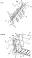
- FIG. 1 is a schematic 3D representation of an optoelectronic sensor S according to the invention shown, wherein the outer housing of the optoelectronic sensor S according to the invention is hidden.
- the optoelectronic sensor S according to the invention has at least one electronic card 1, on which the electronic elements 2 of the optoelectronic sensor S according to the invention are plugged. On the electronic board 1 further light emitter elements and / or light receiving elements of the optoelectronic sensor S according to the invention are plugged, which in the shown FIG. 1 are covered by optical modules 3.1, 3.2, 3.3.
- the illustrated preferred embodiment of the optoelectronic sensor S according to the invention has a single electronic card 1 and three optical modules 3.1, 3.2, 3.3, wherein the three optical modules 3.1, 3.2, 3.3 are locked by means of headband 4 to the electronic board 1.
- the electronic card 1 has a plug 5, with which the electronic card 1 can be electrically connected to further, not shown electronic cards, so that a cascading of the optoelectronic sensor S according to the invention would be possible.
- the illustrated optical modules 3.1, 3.2, 3.3 each comprise a tube array 3a, which has a multiplicity of tubes 3b, in the preferred embodiment shown, 19 tubes 3b.
- Each optical module 3.1, 3.2, 3.3 comprises an open end 6 and a closed end 7.
- connecting tubes 8 explained in more detail below are shown, which are each arranged between two optical modules 3.1, 3.2, 3.3 according to the invention.
- a single inventive optical module 3.1 is in the FIG. 2 shown schematically in 3D.
- the optical module 3.1 according to the invention comprises the tube array 3a with the exemplary 19 tubes 3b, the open end 6 and the closed end 7.
- the open end 6 of the optical module 3.1 according to the invention consists of an open first connecting element 6.1 of a connection of the tube array 3a.
- the open end 6 of the optical module 3.1 according to the invention comprises wall connecting elements 6.2, which preferably form a C-shape at the open end 6 of the optical module 3.1 according to the invention with the open first connecting element 6.1.
- the closed end 7 of the optical module 3.1 consists of a closed second connecting element 7.1 of the connection, wherein the closed second connecting element 7.1 has an outer wall 8d.
- the outer wall of the closed second connecting element 7.1 is formed in such a form-fitting manner to the wall connecting elements 6.2 of the open end 6 of the optical module 3.1 according to the invention, so that when an open end 6 of an optical module according to the invention, for example the module 3.1 in the FIG. 1 , and a closed end 7 of an optical module according to the invention, for example of the module 3.1 in the FIG. 1 , the two connecting elements 6.1 and 7.1 of the compound in the FIG. 1 form gleichsstubus 8 shown, wherein the connecting tube 8 is equal to the 19 tubes 3b of the tube array 3a.
- the connecting tube 8 which is for a light emitting element or light receiving element located at the junction the electronic card 1 can act as a tube.
- the connecting tube 8 has identical geometries and optical properties as the other 19 tubes 3b of the tube array 3a of the optical modules 3.1, 3.2, 3.3 according to the invention.
- FIG. 2A is a 3D detailed representation of the open end 6 and the open first connecting element 6.1 of the optical module 3.1 according to the invention shown.
- the open first connecting element 6.1 consists of three side walls 9a, 9b, 9c of the connecting tube 8 and is open towards the end of the optical module 3.1 according to the invention.
- the three side walls comprise a wide partition wall 8a which separates the first open connection element 6.1 from the inside tube 3b of the tube array 3a and two narrower connection walls 8b and 8c compared to the wide partition 8a.
- a wall connecting element 6.2 is arranged in each case, so that the wall connecting elements 6.2, the connecting walls 8b and 8c, and the partition wall 8a together represent the mentioned C-shape.
- the wall connecting elements 6.2 are open on the side directed towards the electronic card 1, so that when an optical module 3.3 according to the invention is already plugged into the electronic card 1, the first open connecting element 6.1 of the further optical module 3.2 according to the invention is already on the second closed connecting element 7.1 plugged optical module 3.3 according to the invention in the direction of the electronic board 1 can be easily plugged.
- the wall connecting elements 6.2 are closed by means of wall elements 6.3.
- the wall elements 6.3 are used on the one hand when plugging the optical modules 3.1, 3.2, 3.3 as a stop and on the other hand in operation as an optical shield for the kausstubus 8.
- no stray light from / in the kausstubus 8 on / from the / the adjacent tube 3b crosstalk of the infected optical module according to the invention.
- the wall connecting elements 6.2 each have a groove 6.4, which are provided on an inner side of the wall connecting elements 6.2 and are closed at one end by the wall elements 6.3, so that the grooves are arranged opposite 6.4 and the second closed connection element 7.1 in the grooves 6.4 can be inserted.
- the grooves 6.4 guide the second closed connection element 7.1 when mating the optical modules 3.1, 3.2, 3.3 according to the invention, whereby a precise mating is additionally made possible.
- the second closed connection element 7.1 forms the outer wall 8d of the last tube 3b of the optical module 3.1 according to the invention.
- the outer wall 8d is positively connected to the wall connection elements 6.2 of the first open connection element 6.1.
- the geometric dimensions of the outer wall 8d are designed such that in a mated state of the outer wall 8d in the grooves 6.4 of the wall connection elements 6.2, ie mounted state of the first open connection element 6.1 with the second closed connection element 7.1, the connecting tube 8 with identical geometric dimensions how the other tubes 3b of the optical module 3.1, 3.2, 3.3 according to the invention is formed.
- connection tube 8 has the same optical characteristics as the other tubes 3b of the optical module 3.1, 3.2, 3.3 according to the invention.
- the tubes 3b may be matt in the region of the light guide, have a ribbed structure or be provided with a light-absorbing layer, so that the interference signal suppression can be improved.
- the wall connection elements 6.2 of the open end 6 of the optical module 3.1, 3.2, 3.3 according to the invention comprise locking elements which interlock the optical modules 3.1, 3.2, 3.3 according to the invention.
- the locking elements can be, for example, latching hooks.
- the optical modules 3.1, 3.2, 3.3 according to the invention in the assembled state have a high stability, so that the electronic cards 1, on which the assembled optical modules 3.1, 3.2, 3.3 are mounted, can also be mounted stably and precisely to each other.
- On additional holding means or plastic connector means for aligning and holding adjacent electronic cards 1 can be waived accordingly.
Landscapes
- Physics & Mathematics (AREA)
- General Physics & Mathematics (AREA)
- Spectroscopy & Molecular Physics (AREA)
- Life Sciences & Earth Sciences (AREA)
- General Life Sciences & Earth Sciences (AREA)
- Geophysics (AREA)
- Optical Couplings Of Light Guides (AREA)
- Switches Operated By Changes In Physical Conditions (AREA)
Abstract
Description
- Die Erfindung betrifft einen optoelektronischen Sensor mit mindestens einer Elektronikkarte, die Lichtsenderelemente und/oder Lichtempfangselemente aufweist, und mit zumindest zwei optischen Modulen, die auf der Elektronikarte befestigbar sind.
- In der Automatisierungsindustrie werden optoelektronische Sensoren eingesetzt, um eine Arbeitsumgebung einer gefahrbringenden Maschine oder den Zugang zu der Arbeitsumgebung der gefahrbringenden Maschine zu überwachen oder generell ein Objekt zu erfassen.
- Zu den optoelektronischen Sensoren zählen zum Beispiel Lichtschranken, die nach dem Prinzip arbeiten, einen Lichtstrahl mittels der Lichtsenderelementen auszusenden, in den Lichtempfangselementen zu registrieren und zu bewerten, ob das Empfangssignal eine Schaltschwelle über-/unterschreitet oder nicht. In einem solchen Lichtgitter werden effektiv mehrere Lichtschranken parallel zueinander zusammengefügt, so dass ein definierter Bereich durch die Lichtschranken beleuchtet wird. Es ist bekannt, Lichtgitter modular aufzubauen, so dass eine Kaskadierung von Lichtgittern erwünscht ist, um einen größeren definierten überwachten Bereich zu ermöglichen.
- Bei der Kaskadierung werden mehrere Lichtgitter miteinander verbunden, wobei mehrere Elektronikkarten mit Lichtsenderelementen und/oder Lichtempfangselementen miteinander verbunden werden können. Hierbei wird eine hohe Auflösung von den Lichtgittern angestrebt, wobei ein Raster der Lichtgitter kleiner wird. Dadurch werden die Lichtsenderelemente und/oder die Lichtempfangselemente und insbesondere die Abstände zwischen den Lichtsenderelementen und/oder den Lichtempfangselementen kleiner.
- Um gegenseitige Beeinflussung der Lichtstrahlen der Lichtsenderelemente oder Umspiegelungseffekte zu minimieren, die die Messgenauigkeit der Lichtgitter reduziert, und Simultanscan, d. h. mehrere Lichtsenderelemente und/oder Lichtempfangselemente sind gleichzeitig aktiv, zu ermöglichen, muss ein Ausstrahl- bzw. Empfangswinkel für jedes Lichtsenderelement bzw. Lichtempfangselement eingeschränkt werden. D. h. der Ausstrahlwinkel jedes Lichtsenderelement bzw. der Empfangswinkel jedes Lichtempfangselement wird durch sogenannte Kanäle eingeschränkt. Dies wird bei Lichtgittern üblicherweise mit optischen Modulen gewährleistet. Jedes optische Modul weist mindestens ein Tubusarray auf, wobei die Tuben des Tubusarrays die Kanäle bilden.
- Somit verhindern die Tuben des Tubusarrays der optischen Module ein optisches Übersprechen zwischen den Lichtsenderelementen und/oder den Lichtempfangselementen.
- Es ist daher die Aufgabe der vorliegenden Erfindung, einen optoelektronischen Sensor derart zu verbessern, dass eine Kaskadierung einfach und ohne optisches Übersprechen an den Verbindungsstellen erzielbar ist.
- Die Aufgabe wird erfindungsgemäß gelöst durch einen optoelektronischen Sensor mit mindestens einer Elektronikkarte, die Lichtsenderelemente und/oder Lichtempfangselemente aufweist, und mit zumindest zwei optischen Modulen, die auf der Elektronikarte befestigbar sind, wobei jedes optische Modul ein Tubusarray, das eine Vielzahl von Tuben aufweist, ein offenes Ende und ein geschlossenes Ende umfasst, wobei das offene Ende des optischen Moduls aus einem offenen ersten Verbindungselement einer Verbindung des Tubusarrays besteht und Wandverbindungselemente umfasst, und das geschlossene Ende des optischen Moduls aus einem geschlossenen zweiten Verbindungselement der Verbindung besteht, das eine Außenwand aufweist, die derart formschlüssig zu den Wandverbindungselementen des offenen Endes des optischen Moduls ausgebildet ist, so dass bei einem Zusammenstecken eines offenen Endes eines optischen Moduls und eines geschlossenen Endes eines weiteren optischen Moduls die beiden Verbindungselemente der Verbindung einen Verbindungstubus bilden, der den Tuben des Tubusarrays gleicht.
- Gemäß einem bevorzugten Ausführungsbeispiel besteht das offene erste Verbindungselement aus drei Seitenwänden des Verbindungstubus' und ist zum Ende des optischen Moduls hin offen.
- Gemäß einem weiteren bevorzugten Ausführungsbeispiel bildet die Außenwand des geschlossenen zweiten Verbindungselements eine vierte Seitenwand des Verbindungstubus, wenn das erste und zweite Verbindungselement ineinander gesteckt sind.
- Gemäß einem weiteren bevorzugten Ausführungsbeispiel sind die Wandverbindungselemente an gegenüberliegenden Verbindungswänden des offenen ersten Verbindungselements angeordnet.
- Gemäß einem weiteren bevorzugten Ausführungsbeispiel bilden die Wandverbindungselemente mit dem offenen ersten Verbindungselement eine C-Form. Hieraus ergibt sich der Vorteil, dass im zusammengesteckten Zustand der ersten und zweiten Verbindungselemente der Verbindung die Wandverbindungselemente den gebildeten Verbindungstubus optisch abschirmen. D. h. kein Licht kann durch die Spalten zwischen den Seitenwänden des ersten und zweiten Verbindungselements aus- bzw. eintreten.
- Gemäß einem weiteren bevorzugten Ausführungsbeispiel sind die Wandverbindungselemente auf der zu der Elektronikkarte gerichteten Seite offen, so dass das offene erste Verbindungselement auf das geschlossene zweite Verbindungselement in Richtung der Elektronikkarte aufsteckbar ist. Daraus ergibt sich der Vorteil, dass ein präzises Zusammenstecken der optischen Module möglich ist. Ferner wird der Zusammenbau des optoelektronischen Sensors erleichtert, so dass Produktionskosten reduziert werden können.
- Gemäß einem weiteren bevorzugten Ausführungsbeispiel sind die Wandverbindungselemente auf der von der Elektronikkarte abgewandten Seite mittels Wandelemente geschlossen. Hierdurch ist der Verbindungstubus auch in Richtung einer optischen Achse des optoeletronischen Sensors vorteilhafterweise optisch abgeschirmt.
- Gemäß einem weiteren bevorzugten Ausführungsbeispiel weisen die Wandverbindungselemente jeweils eine Nut auf, in die das geschlossene zweite Verbindungselement einschiebbar ist. Es ergibt sich der Vorteil, dass bei der Montage der optischen Module eine genaue Führung der Module gegeben ist.
- Gemäß einem weiteren bevorzugten Ausführungsbeispiel ist die Nut auf einer Innenseite des jeweiligen Wandverbindungselements vorgesehen, so dass die Nuten gegenüberliegend angeordnet sind.
- Gemäß einem weiteren bevorzugten Ausführungsbeispiel weist der Verbindungstubus eine gleiche Geometrie und Wandoberflächenbeschaffenheit wie die Tuben des Tubusarrays auf. Hierdurch hat der Verbindungstubus vorteilhafterweise die gleichen optischen Eigenschaften wie die Tuben der optischen Module.
- Gemäß einem weiteren bevorzugten Ausführungsbeispiel umfassen die Wandverbindungselemente Verriegelungselemente zum Verriegeln der optischen Module untereinander.
- Der erfindungsgemäße optoelektronische Sensor kann auf ähnliche Weise durch weitere Merkmale ausgestaltet werden und zeigt dabei ähnliche Vorteile. Derartige weitere Merkmale sind beispielhaft, aber nicht abschließend, in den sich an dem unabhängigen Anspruch anschließenden Unteransprüchen beschrieben.
- Die Erfindung wird nachstehend auch hinsichtlich weiterer Vorteile und Merkmale unter Bezugnahme auf die beigefügte Zeichnung anhand von Ausführungsbeispielen erläutert. Die Figuren der Zeichnung zeigen in:
- Fig. 1
- eine schematische 3D-Darstellung eines erfindungsgemäßen optoelektronischen Sensors ohne ein Außengehäuse;
- Fig. 2
- eine schematische 3D-Darstellung eines erfindungsgemäßen optischen Moduls;
- Fig. 2A
- eine schematische 3D-Detaildarstellung eines offenen Endes des erfindungsgemäßen optischen Moduls; und
- Fig. 2B
- eine schematische 3D-Detaildarstellung eines geschlossenen Endes des erfindungsgemäßen optischen Moduls.
- In der
Figur 1 ist eine schematische 3D-Darstellung eines erfindungsgemäßen optoelektronischen Sensors S gezeigt, wobei das Außengehäuse des erfindungsgemäßen optoelektronischen Sensors S ausgeblendet ist. - Der erfindungsgemäße optoelektronische Sensors S weist zumindest eine Elektronikkarte 1 auf, auf der die Elektronikelemente 2 des erfindungsgemäßen optoelektronischen Sensors S aufgesteckt sind. Auf die Elektronikkarte 1 sind ferner Lichtsenderelemente und/oder Lichtempfangselemente des erfindungsgemäßen optoelektronischen Sensors S aufgesteckt, die in der gezeigten
Figur 1 durch optische Module 3.1, 3.2, 3.3 überdeckt sind. - Das dargestellte bevorzugte Ausführungsbeispiel des erfindungsgemäßen optoelektronischen Sensors S weist eine einzige Elektronikkarte 1 und drei optische Module 3.1, 3.2, 3.3 auf, wobei die drei optischen Module 3.1, 3.2, 3.3 mittels Haltebügel 4 an die Elektronikkarte 1 arretiert sind. Die Elektronikkarte 1 weist einen Stecker 5 auf, mit dem die Elektronikkarte 1 mit weiteren, nicht-dargestellten Elektronikkarten elektrisch verbunden werden kann, so dass eine Kaskadierung des erfindungsgemäßen optoelektronischen Sensors S möglich wäre.
- Die dargestellten optischen Module 3.1, 3.2, 3.3 umfasst jeweils ein Tubusarray 3a, das eine Vielzahl von Tuben 3b, in dem gezeigten bevorzugten Ausführungsbeispiel 19 Tuben 3b, aufweist. Jedes optische Modul 3.1, 3.2, 3.3 umfasst ein offenes Ende 6 und ein geschlossenes Ende 7.
- Aus der gezeigten
Figur 1 sind das offene Ende 6 des dritten optischen Moduls 3.3 und das geschlossene Ende 7 des ersten optischen Moduls 3.1 zu sehen. - Ferner sind zwei, nachfolgend noch näher erläuterte Verbindungstuben 8 gezeigt, die jeweils zwischen zwei erfindungsgemäßen optischen Module 3.1, 3.2, 3.3 angeordnet sind.
- Ein einzelnes erfindungsgemäßes optisches Modul 3.1 ist in der
Figur 2 schematisch in 3D dargestellt. Das erfindungsgemäße optische Modul 3.1 umfasst das Tubusarray 3a mit den beispielhaften 19 Tuben 3b, das offene Ende 6 und das geschlossene Ende 7. Das offene Ende 6 des erfindungsgemäßen optischen Moduls 3.1 besteht aus einem offenen ersten Verbindungselement 6.1 einer Verbindung des Tubusarrays 3a. Weiterhin umfasst das offene Ende 6 des erfindungsgemäßen optischen Moduls 3.1 Wandverbindungselemente 6.2, die vorzugsweise mit dem offenen ersten Verbindungselement 6.1 eine C-Form an dem offenen Ende 6 des erfindungsgemäßen optischen Moduls 3.1 bilden. - Das geschlossene Ende 7 des erfindungsgemäßen optischen Moduls 3.1 besteht aus einem geschlossenen zweiten Verbindungselement 7.1 der Verbindung, wobei das geschlossene zweite Verbindungselement 7.1 eine Außenwand 8d aufweist.
- Erfindungsgemäß ist die Außenwand des geschlossenen zweiten Verbindungselements 7.1 derart formschlüssig zu den Wandverbindungselementen 6.2 des offenen Endes 6 des erfindungsgemäßen optischen Moduls 3.1 ausgebildet, so dass bei einem Zusammenstecken eines offenen Endes 6 eines erfindungsgemäßen optischen Moduls, zum Beispiel des Moduls 3.1 in der
Figur 1 , und eines geschlossenen Endes 7 eines erfindungsgemäßen optischen Moduls, zum Beispiel des Moduls 3.1 in derFigur 1 , die beiden Verbindungselemente 6.1 und 7.1 der Verbindung einen in derFigur 1 gezeigten Verbindungstubus 8 bilden, wobei der Verbindungstubus 8 den 19 Tuben 3b des Tubusarrays 3a gleicht. - D. h. mit anderen Worten, wenn ein erfindungsgemäßes optisches Modul 3.1 bzw. 3.2 mit einem weiteren erfindungsgemäßen optischen Modul 3.2 bzw. 3.3 zusammengesteckt wird, um eine Kaskadierung zu ermöglichen, bilden das offene Ende 6 des einen erfindungsgemäßen optischen Moduls 3.1 bzw. 3.2 und das geschlossene Ende 7 des anderen erfindungsgemäßen optischen Moduls 3.2 bzw. 3.3 den Verbindungstubus 8, der für ein an der Verbindungsstelle befindliches Lichtsenderelement oder Lichtempfangselement der Elektronikkarte 1 als Tubus fungieren kann. Hierbei weist der Verbindungstubus 8 identische Geometrien und optische Eigenschaften wie die anderen 19 Tuben 3b des Tubusarrays 3a der erfindungsgemäßen optischen Module 3.1, 3.2, 3.3 auf.
- In der
Figur 2A ist eine 3D-Detaildarstellung des offenen Endes 6 bzw. des offenen ersten Verbindungselements 6.1 des erfindungsgemäßen optischen Moduls 3.1 gezeigt. Hierbei besteht das offene erste Verbindungselement 6.1 aus drei Seitenwänden 9a, 9b, 9c des Verbindungstubus 8 und ist zum Ende des erfindungsgemäßen optischen Moduls 3.1 hin offen. Die drei Seitenwände umfassen eine breite Trennwand 8a, die das erste offene Verbindungselement 6.1 von dem innenliegenden Tubus 3b des Tubusarrays 3a trennt, und zwei im Vergleich zu der breiten Trennwand 8a schmaleren Verbindungswände 8b und 8c. - An den Verbindungswänden 8b und 8c ist jeweils ein Wandverbindungselement 6.2 angeordnet, so dass die Wandverbindungselemente 6.2, die Verbindungswände 8b und 8c, und die Trennwand 8a zusammen die erwähnte C-Form darstellen.
- Die Wandverbindungselemente 6.2 sind auf der zu der Elektronikkarte 1 gerichteten Seite offen, so dass, wenn ein erfindungsgemäßes optisches Modul 3.3 bereits auf die Elektronikkarte 1 gesteckt ist, das erste offene Verbindungselement 6.1 des weiteren erfindungsgemäßen optischen Moduls 3.2 auf das zweite geschlossene Verbindungselement 7.1 des bereits gesteckten erfindungsgemäßen optischen Moduls 3.3 in Richtung der Elektronikkarte 1 einfach aufgesteckt werden kann.
- Auf der von der Elektronikkarte 1 abgewandten Seite sind die Wandverbindungselemente 6.2 mittels Wandelemente 6.3 geschlossen. Die Wandelemente 6.3 dienen einerseits beim Zusammenstecken der erfindungsgemäßen optischen Module 3.1, 3.2, 3.3 als Anschlag und andererseits im Betrieb als optische Abschirmung für den gebildeten Verbindungstubus 8. Dadurch kann kein Störlicht aus/in dem Verbindungstubus 8 auf/von den/dem benachbarten Tubus 3b des angesteckten erfindungsgemäßen optischen Moduls übersprechen.
- Zum Erleichtern des Zusammensteckens der beiden Verbindungselementen 6.1 und 7.1 der Verbindung weisen die Wandverbindungselemente 6.2 jeweils eine Nut 6.4 auf, die auf einer Innenseite der Wandverbindungselemente 6.2 vorgesehen sind und an einem Ende durch die Wandelemente 6.3 abgeschlossen sind, so dass die Nuten 6.4 gegenüberliegend angeordnet sind und das zweite geschlossene Verbindungselement 7.1 in die Nuten 6.4 einschiebbar ist.
- Die Nuten 6.4 führen das zweite geschlossene Verbindungselement 7.1 beim Zusammenstecken der erfindungsgemäßen optischen Module 3.1, 3.2, 3.3, wodurch ein präzises Zusammenstecken zusätzlich ermöglicht wird.
- Wie in der
Figur 2B gezeigt, die eine 3D-Detaildarstellung des geschlossenen Endes 7, insbesondere des zweiten geschlossenen Verbindungselements 7.1, des erfindungsgemäßen optischen Moduls 3.1 darstellt, bildet das zweite geschlossene Verbindungselement 7.1 die Außenwand 8d des letzten Tubus 3b des erfindungsgemäßen optischen Moduls 3.1. Hierbei ist die Außenwand 8d formschlüssig zu den Wandverbindungselementen 6.2 des ersten offenen Verbindungselements 6.1. Zusätzlich sind die geometrischen Maße der Außenwand 8d derart ausgelegt, so dass in einem zusammengesteckten Zustand der Außenwand 8d in den Nuten 6.4 der Wandverbindungselemente 6.2, d. h. montierter Zustand des ersten offenen Verbindungselements 6.1 mit dem zweiten geschlossenen Verbindungselement 7.1, der Verbindungstubus 8 mit identischen geometrischen Maßen wie die übrigen Tuben 3b des erfindungsgemäßen optischen Moduls 3.1, 3.2, 3.3 gebildet ist. - Ferner sind die Geometrien und Oberflächen der Innenflächen der ersten offenen und zweiten geschlossenen Verbindungselemente 6.1 und 7.1, d. h. der Trennwand 8a, der Verbindungswände 8b und 8c und der Außenwand 8d, derart ausgebildet, dass der gebildete Verbindungstubus 8 die gleichen optischen Eigenschaften wie die übrigen Tuben 3b des erfindungsgemäßen optischen Moduls 3.1, 3.2, 3.3 aufweist. Hierbei können die Tuben 3b im Bereich der Lichtführung matt sein, eine Rippenstruktur aufweisen oder mit einer lichtabsorbierenden Schicht versehen sein, so dass die Störsignalunterdrückung verbessert werden kann.
- Zusätzlich umfassen die Wandverbindungselemente 6.2 des offenen Endes 6 des erfindungsgemäßen optischen Moduls 3.1, 3.2, 3.3 Verriegelungselemente, die die erfindungsgemäßen optischen Module 3.1, 3.2, 3.3 untereinander verriegeln. Die Verriegelungselemente können beispielweise Rasthaken sein. Hierdurch weisen die erfindungsgemäßen optischen Module 3.1, 3.2, 3.3 im zusammengesteckten Zustand eine hohe Stabilität auf, so dass die Elektronikkarten 1, auf die die zusammengesteckten erfindungsgemäßen optischen Module 3.1, 3.2, 3.3 montiert sind, ebenfalls stabil und präzise zueinander montiert sein können. Auf zusätzliche Haltemittel oder Kunststoffverbindermittel zum Ausrichten und Halten benachbarte Elektronikkarten 1 kann entsprechend verzichtet werden.
-
- 1
- Elektronikkarte
- 2
- Elektronikelemente
- 3.1,3.2, 3.3
- Optische Module
- 3a
- Tubusarray
- 3b
- Tubus/Tuben
- 4
- Haltebügeln
- 5
- Stecker
- 6
- Offenes Ende des optischen Moduls
- 6.1
- Offenes erstes Verbindungselement
- 6.2
- Wandverbindungselement
- 6.3
- Wandelement
- 6.4
- Nut
- 7
- Geschlossenes Ende des optischen Moduls
- 7.1
- Geschlossenes zweites Verbindungselement
- 8
- Verbindungstubus
- 8a
- Trennwand
- 8b, 8c
- Verbindungswand
- 8d
- Außenwand
- S
- Optoelektronischer Sensor
Claims (11)
- Optoelektronischer Sensor (S) mit mindestens einer Elektronikkarte (1), die Lichtsenderelemente und/oder Lichtempfangselemente aufweist, und mit zumindest zwei optischen Modulen (3.1, 3.2, 3.3), die auf der Elektronikarte (1) befestigbar sind,
wobei jedes optische Modul (3.1, 3.2, 3.3) ein Tubusarray (3a), das eine Vielzahl von Tuben (3b) aufweist, ein offenes Ende (6) und ein geschlossenes Ende (7) umfasst,
wobei das offene Ende (6) des optischen Moduls (3.1, 3.2, 3.3) aus einem offenen ersten Verbindungselement (6.1) einer Verbindung des Tubusarrays (3a) besteht und Wandverbindungselemente (6.2) umfasst, und das geschlossene Ende (7) des optischen Moduls (3.1, 3.2, 3.3) aus einem geschlossenen zweiten Verbindungselement (7.1) der Verbindung besteht, das eine Außenwand (8d) aufweist, die derart formschlüssig zu den Wandverbindungselementen (6.2) des offenen Endes (6) des optischen Moduls (3.1, 3.2, 3.3) ausgebildet ist, so dass bei einem Zusammenstecken eines offenen Endes (6) eines optischen Moduls (3.1) und eines geschlossenen Endes (7) eines weiteren optischen Moduls (3.2) die beiden Verbindungselemente (6.1, 7.1) der Verbindung einen Verbindungstubus (8) bilden, der den Tuben (3b) des Tubusarrays (3a) gleicht. - Optoelektronischer Sensor (S) nach Anspruch 1, wobei das offene erste Verbindungselement (6.1) aus drei Seitenwänden des Verbindungstubus (8) besteht und zum Ende des optischen Moduls (3.1, 3.2, 3.3) hin offen ist.
- Optoelektronischer Sensor (S) nach Anspruch 1 oder 2, wobei die Außenwand (8d) des geschlossenen zweiten Verbindungselements (7.1) eine vierte Seitenwand des Verbindungstubus' (8) bildet, wenn das erste und zweite Verbindungselement (6.1, 7.1) ineinander gesteckt sind.
- Optoelektronischer Sensor (S) nach einem der vorhergehenden Ansprüche, wobei die Wandverbindungselemente (6.2) an gegenüberliegenden Verbindungswänden (8b, 8c) des offenen ersten Verbindungselements (6.1) angeordnet sind.
- Optoelektronischer Sensor (S) nach einem der vorhergehenden Ansprüche, wobei die Wandverbindungselemente (6.2) mit dem offenen ersten Verbindungselement (6.1) eine C-Form bilden.
- Optoelektronischer Sensor (S) nach einem der vorhergehenden Ansprüche, wobei die Wandverbindungselemente (6.2) auf der zu der Elektronikkarte (1) gerichteten Seite offen sind, so dass das offene erste Verbindungselement (6.1) auf das geschlossene zweite Verbindungselement (7.1) in Richtung der Elektronikkarte (1) aufsteckbar ist.
- Optoelektronischer Sensor (S) nach einem der vorhergehenden Ansprüche, wobei die Wandverbindungselemente (6.2) auf der von der Elektronikkarte (1) abgewandten Seite mittels Wandelemente (6.3) geschlossen sind.
- Optoelektronischer Sensor (S) nach einem der vorhergehenden Ansprüche, wobei die Wandverbindungselemente (6.2) jeweils eine Nut (6.4) aufweisen, in die (6.4) das geschlossene zweite Verbindungselement (7.1) einschiebbar ist.
- Optoelektronischer Sensor (S) nach Anspruch 8, wobei die Nut (6.4) auf einer Innenseite des jeweiligen Wandverbindungselements (6.2) vorgesehen ist, so dass die Nuten (6.4) gegenüberliegend angeordnet sind.
- Optoelektronischer Sensor (S) nach einem der vorhergehenden Ansprüche, wobei der Verbindungstubus (8) eine gleiche Geometrie und Wandoberflächenbeschaffenheit wie die Tuben (3b) des Tubusarrays (3a) aufweist.
- Optoelektronischer Sensor (S) nach einem der vorhergehenden Ansprüche, wobei die Wandverbindungselemente (6.2) Verriegelungselemente zum Verriegeln der optischen Module (3.1, 3.2, 3.3) untereinander umfassen.
Applications Claiming Priority (1)
| Application Number | Priority Date | Filing Date | Title |
|---|---|---|---|
| DE202015102596.3U DE202015102596U1 (de) | 2015-05-20 | 2015-05-20 | Optoelektronischer Sensor |
Publications (2)
| Publication Number | Publication Date |
|---|---|
| EP3096162A1 true EP3096162A1 (de) | 2016-11-23 |
| EP3096162B1 EP3096162B1 (de) | 2017-08-30 |
Family
ID=55521585
Family Applications (1)
| Application Number | Title | Priority Date | Filing Date |
|---|---|---|---|
| EP16159239.9A Active EP3096162B1 (de) | 2015-05-20 | 2016-03-08 | Optoelektronischer sensor |
Country Status (4)
| Country | Link |
|---|---|
| US (1) | US9874473B2 (de) |
| EP (1) | EP3096162B1 (de) |
| DE (1) | DE202015102596U1 (de) |
| ES (1) | ES2645718T3 (de) |
Families Citing this family (1)
| Publication number | Priority date | Publication date | Assignee | Title |
|---|---|---|---|---|
| DE202019105868U1 (de) | 2019-10-22 | 2019-10-31 | Sick Ag | Optoelektronischer Sensor |
Citations (5)
| Publication number | Priority date | Publication date | Assignee | Title |
|---|---|---|---|---|
| JPH11329179A (ja) * | 1998-05-06 | 1999-11-30 | Keyence Corp | 導体接続部を有する枠体の連結装置 |
| EP1577684A1 (de) * | 2004-03-16 | 2005-09-21 | Sick Ag | Lichtgitter |
| EP1770414A1 (de) * | 2005-09-28 | 2007-04-04 | Sick Ag | Optoelektronische Anordnung |
| EP2511737A1 (de) * | 2011-04-13 | 2012-10-17 | Cedes Safety & Automation AG | Modularer Lichtvorhang und optische Einheit für einen Lichtvorhang |
| DE202013104607U1 (de) * | 2013-10-11 | 2015-01-12 | Sick Ag | Optisches Modul |
Family Cites Families (5)
| Publication number | Priority date | Publication date | Assignee | Title |
|---|---|---|---|---|
| JPH0690900B2 (ja) * | 1988-11-14 | 1994-11-14 | 株式会社キーエンス | 多光軸光電スイッチ |
| US6680469B2 (en) * | 2000-03-10 | 2004-01-20 | Scientific Technologies Incorporated | Segmented light curtain with keyed interfaces |
| JP3927503B2 (ja) * | 2003-01-20 | 2007-06-13 | 株式会社キーエンス | 多光軸光電センサ |
| EP2730952B1 (de) * | 2012-11-09 | 2018-08-29 | Sick Ag | Lichtgitter |
| JP6084522B2 (ja) * | 2013-06-21 | 2017-02-22 | 株式会社キーエンス | 多光軸光電センサ |
-
2015
- 2015-05-20 DE DE202015102596.3U patent/DE202015102596U1/de not_active Expired - Lifetime
-
2016
- 2016-03-08 ES ES16159239.9T patent/ES2645718T3/es active Active
- 2016-03-08 EP EP16159239.9A patent/EP3096162B1/de active Active
- 2016-05-13 US US15/153,893 patent/US9874473B2/en active Active
Patent Citations (5)
| Publication number | Priority date | Publication date | Assignee | Title |
|---|---|---|---|---|
| JPH11329179A (ja) * | 1998-05-06 | 1999-11-30 | Keyence Corp | 導体接続部を有する枠体の連結装置 |
| EP1577684A1 (de) * | 2004-03-16 | 2005-09-21 | Sick Ag | Lichtgitter |
| EP1770414A1 (de) * | 2005-09-28 | 2007-04-04 | Sick Ag | Optoelektronische Anordnung |
| EP2511737A1 (de) * | 2011-04-13 | 2012-10-17 | Cedes Safety & Automation AG | Modularer Lichtvorhang und optische Einheit für einen Lichtvorhang |
| DE202013104607U1 (de) * | 2013-10-11 | 2015-01-12 | Sick Ag | Optisches Modul |
Also Published As
| Publication number | Publication date |
|---|---|
| EP3096162B1 (de) | 2017-08-30 |
| ES2645718T3 (es) | 2017-12-07 |
| US9874473B2 (en) | 2018-01-23 |
| DE202015102596U1 (de) | 2016-08-23 |
| US20160341599A1 (en) | 2016-11-24 |
Similar Documents
| Publication | Publication Date | Title |
|---|---|---|
| DE102004046725B4 (de) | Gehäuse für ein Lichtgitter | |
| EP3961821A1 (de) | Verbindungsvorrichtung mit einem steckverbinder und einem gegensteckverbinder | |
| DE112015000415B4 (de) | Passaufbau für einen optischen Stecker und optischer Stecker | |
| EP2019293B1 (de) | Gehäuse für eine optoelektronische Sensoranordnung | |
| EP4170832A1 (de) | Steckverbinderanordnung zum verbinden von signalleitern | |
| EP3096162B1 (de) | Optoelektronischer sensor | |
| EP2730952B1 (de) | Lichtgitter | |
| EP3008500B1 (de) | Lichtgitterbauteil | |
| DE202008004711U1 (de) | Lichtgitterkaskadierung | |
| EP1978378B1 (de) | Optoelektronische Sensoranordnung | |
| DE202007007290U1 (de) | Optoelektronische Sensoranordnung | |
| DE112016000324T5 (de) | Verbinder | |
| DE202014105530U1 (de) | Steckverbinder | |
| EP2657727B1 (de) | Lichtvorhang | |
| EP2954357B1 (de) | Gerätebuchse | |
| EP3770647B1 (de) | Lichtschrankenanordnung und verfahren zur justage einer lichtschrankenanordnung | |
| DE102014111031B4 (de) | Modul, Koppeleinheit und Steuerungssystem | |
| DE202005010358U1 (de) | Optoelektronisches Lichtgitter | |
| DE202011000608U1 (de) | Montageprofil für ein Lichtgittergehäuse und Lichtgitter | |
| EP3324218A1 (de) | Mehrstrahllichtschranke | |
| DE202007010492U1 (de) | Optoelektronische Sensoranordnung | |
| DE102015213631A1 (de) | Schaltungsplatine | |
| DE102015119312A1 (de) | Lichtgitter und Verfahren zum Erfassen von Objekten | |
| EP2926092B1 (de) | Redundante messung der position einer störung im lichtleiter | |
| EP1312940A1 (de) | Lichtschranke mit Lichtwellenleiter |
Legal Events
| Date | Code | Title | Description |
|---|---|---|---|
| PUAI | Public reference made under article 153(3) epc to a published international application that has entered the european phase |
Free format text: ORIGINAL CODE: 0009012 |
|
| 17P | Request for examination filed |
Effective date: 20161012 |
|
| AK | Designated contracting states |
Kind code of ref document: A1 Designated state(s): AL AT BE BG CH CY CZ DE DK EE ES FI FR GB GR HR HU IE IS IT LI LT LU LV MC MK MT NL NO PL PT RO RS SE SI SK SM TR |
|
| AX | Request for extension of the european patent |
Extension state: BA ME |
|
| GRAP | Despatch of communication of intention to grant a patent |
Free format text: ORIGINAL CODE: EPIDOSNIGR1 |
|
| INTG | Intention to grant announced |
Effective date: 20170407 |
|
| GRAJ | Information related to disapproval of communication of intention to grant by the applicant or resumption of examination proceedings by the epo deleted |
Free format text: ORIGINAL CODE: EPIDOSDIGR1 |
|
| INTC | Intention to grant announced (deleted) | ||
| GRAP | Despatch of communication of intention to grant a patent |
Free format text: ORIGINAL CODE: EPIDOSNIGR1 |
|
| GRAS | Grant fee paid |
Free format text: ORIGINAL CODE: EPIDOSNIGR3 |
|
| GRAA | (expected) grant |
Free format text: ORIGINAL CODE: 0009210 |
|
| INTG | Intention to grant announced |
Effective date: 20170707 |
|
| AK | Designated contracting states |
Kind code of ref document: B1 Designated state(s): AL AT BE BG CH CY CZ DE DK EE ES FI FR GB GR HR HU IE IS IT LI LT LU LV MC MK MT NL NO PL PT RO RS SE SI SK SM TR |
|
| REG | Reference to a national code |
Ref country code: GB Ref legal event code: FG4D Free format text: NOT ENGLISH |
|
| REG | Reference to a national code |
Ref country code: CH Ref legal event code: EP |
|
| REG | Reference to a national code |
Ref country code: AT Ref legal event code: REF Ref document number: 924099 Country of ref document: AT Kind code of ref document: T Effective date: 20170915 |
|
| REG | Reference to a national code |
Ref country code: IE Ref legal event code: FG4D Free format text: LANGUAGE OF EP DOCUMENT: GERMAN |
|
| REG | Reference to a national code |
Ref country code: DE Ref legal event code: R096 Ref document number: 502016000117 Country of ref document: DE |
|
| REG | Reference to a national code |
Ref country code: SE Ref legal event code: TRGR |
|
| REG | Reference to a national code |
Ref country code: ES Ref legal event code: FG2A Ref document number: 2645718 Country of ref document: ES Kind code of ref document: T3 Effective date: 20171207 |
|
| REG | Reference to a national code |
Ref country code: NL Ref legal event code: MP Effective date: 20170830 |
|
| REG | Reference to a national code |
Ref country code: LT Ref legal event code: MG4D |
|
| PG25 | Lapsed in a contracting state [announced via postgrant information from national office to epo] |
Ref country code: NO Free format text: LAPSE BECAUSE OF FAILURE TO SUBMIT A TRANSLATION OF THE DESCRIPTION OR TO PAY THE FEE WITHIN THE PRESCRIBED TIME-LIMIT Effective date: 20171130 Ref country code: HR Free format text: LAPSE BECAUSE OF FAILURE TO SUBMIT A TRANSLATION OF THE DESCRIPTION OR TO PAY THE FEE WITHIN THE PRESCRIBED TIME-LIMIT Effective date: 20170830 Ref country code: LT Free format text: LAPSE BECAUSE OF FAILURE TO SUBMIT A TRANSLATION OF THE DESCRIPTION OR TO PAY THE FEE WITHIN THE PRESCRIBED TIME-LIMIT Effective date: 20170830 Ref country code: FI Free format text: LAPSE BECAUSE OF FAILURE TO SUBMIT A TRANSLATION OF THE DESCRIPTION OR TO PAY THE FEE WITHIN THE PRESCRIBED TIME-LIMIT Effective date: 20170830 |
|
| PG25 | Lapsed in a contracting state [announced via postgrant information from national office to epo] |
Ref country code: RS Free format text: LAPSE BECAUSE OF FAILURE TO SUBMIT A TRANSLATION OF THE DESCRIPTION OR TO PAY THE FEE WITHIN THE PRESCRIBED TIME-LIMIT Effective date: 20170830 Ref country code: LV Free format text: LAPSE BECAUSE OF FAILURE TO SUBMIT A TRANSLATION OF THE DESCRIPTION OR TO PAY THE FEE WITHIN THE PRESCRIBED TIME-LIMIT Effective date: 20170830 Ref country code: GR Free format text: LAPSE BECAUSE OF FAILURE TO SUBMIT A TRANSLATION OF THE DESCRIPTION OR TO PAY THE FEE WITHIN THE PRESCRIBED TIME-LIMIT Effective date: 20171201 Ref country code: BG Free format text: LAPSE BECAUSE OF FAILURE TO SUBMIT A TRANSLATION OF THE DESCRIPTION OR TO PAY THE FEE WITHIN THE PRESCRIBED TIME-LIMIT Effective date: 20171130 Ref country code: IS Free format text: LAPSE BECAUSE OF FAILURE TO SUBMIT A TRANSLATION OF THE DESCRIPTION OR TO PAY THE FEE WITHIN THE PRESCRIBED TIME-LIMIT Effective date: 20171230 |
|
| REG | Reference to a national code |
Ref country code: FR Ref legal event code: PLFP Year of fee payment: 3 |
|
| PG25 | Lapsed in a contracting state [announced via postgrant information from national office to epo] |
Ref country code: NL Free format text: LAPSE BECAUSE OF FAILURE TO SUBMIT A TRANSLATION OF THE DESCRIPTION OR TO PAY THE FEE WITHIN THE PRESCRIBED TIME-LIMIT Effective date: 20170830 |
|
| PG25 | Lapsed in a contracting state [announced via postgrant information from national office to epo] |
Ref country code: DK Free format text: LAPSE BECAUSE OF FAILURE TO SUBMIT A TRANSLATION OF THE DESCRIPTION OR TO PAY THE FEE WITHIN THE PRESCRIBED TIME-LIMIT Effective date: 20170830 Ref country code: PL Free format text: LAPSE BECAUSE OF FAILURE TO SUBMIT A TRANSLATION OF THE DESCRIPTION OR TO PAY THE FEE WITHIN THE PRESCRIBED TIME-LIMIT Effective date: 20170830 Ref country code: CZ Free format text: LAPSE BECAUSE OF FAILURE TO SUBMIT A TRANSLATION OF THE DESCRIPTION OR TO PAY THE FEE WITHIN THE PRESCRIBED TIME-LIMIT Effective date: 20170830 |
|
| PG25 | Lapsed in a contracting state [announced via postgrant information from national office to epo] |
Ref country code: EE Free format text: LAPSE BECAUSE OF FAILURE TO SUBMIT A TRANSLATION OF THE DESCRIPTION OR TO PAY THE FEE WITHIN THE PRESCRIBED TIME-LIMIT Effective date: 20170830 Ref country code: SK Free format text: LAPSE BECAUSE OF FAILURE TO SUBMIT A TRANSLATION OF THE DESCRIPTION OR TO PAY THE FEE WITHIN THE PRESCRIBED TIME-LIMIT Effective date: 20170830 Ref country code: SM Free format text: LAPSE BECAUSE OF FAILURE TO SUBMIT A TRANSLATION OF THE DESCRIPTION OR TO PAY THE FEE WITHIN THE PRESCRIBED TIME-LIMIT Effective date: 20170830 |
|
| REG | Reference to a national code |
Ref country code: DE Ref legal event code: R097 Ref document number: 502016000117 Country of ref document: DE |
|
| PLBE | No opposition filed within time limit |
Free format text: ORIGINAL CODE: 0009261 |
|
| STAA | Information on the status of an ep patent application or granted ep patent |
Free format text: STATUS: NO OPPOSITION FILED WITHIN TIME LIMIT |
|
| 26N | No opposition filed |
Effective date: 20180531 |
|
| PG25 | Lapsed in a contracting state [announced via postgrant information from national office to epo] |
Ref country code: SI Free format text: LAPSE BECAUSE OF FAILURE TO SUBMIT A TRANSLATION OF THE DESCRIPTION OR TO PAY THE FEE WITHIN THE PRESCRIBED TIME-LIMIT Effective date: 20170830 |
|
| PG25 | Lapsed in a contracting state [announced via postgrant information from national office to epo] |
Ref country code: MT Free format text: LAPSE BECAUSE OF FAILURE TO SUBMIT A TRANSLATION OF THE DESCRIPTION OR TO PAY THE FEE WITHIN THE PRESCRIBED TIME-LIMIT Effective date: 20170830 |
|
| PG25 | Lapsed in a contracting state [announced via postgrant information from national office to epo] |
Ref country code: MC Free format text: LAPSE BECAUSE OF FAILURE TO SUBMIT A TRANSLATION OF THE DESCRIPTION OR TO PAY THE FEE WITHIN THE PRESCRIBED TIME-LIMIT Effective date: 20170830 |
|
| REG | Reference to a national code |
Ref country code: BE Ref legal event code: MM Effective date: 20180331 |
|
| REG | Reference to a national code |
Ref country code: IE Ref legal event code: MM4A |
|
| PG25 | Lapsed in a contracting state [announced via postgrant information from national office to epo] |
Ref country code: LU Free format text: LAPSE BECAUSE OF NON-PAYMENT OF DUE FEES Effective date: 20180308 |
|
| PG25 | Lapsed in a contracting state [announced via postgrant information from national office to epo] |
Ref country code: IE Free format text: LAPSE BECAUSE OF NON-PAYMENT OF DUE FEES Effective date: 20180308 |
|
| PG25 | Lapsed in a contracting state [announced via postgrant information from national office to epo] |
Ref country code: BE Free format text: LAPSE BECAUSE OF NON-PAYMENT OF DUE FEES Effective date: 20180331 |
|
| PG25 | Lapsed in a contracting state [announced via postgrant information from national office to epo] |
Ref country code: TR Free format text: LAPSE BECAUSE OF FAILURE TO SUBMIT A TRANSLATION OF THE DESCRIPTION OR TO PAY THE FEE WITHIN THE PRESCRIBED TIME-LIMIT Effective date: 20170830 |
|
| PG25 | Lapsed in a contracting state [announced via postgrant information from national office to epo] |
Ref country code: PT Free format text: LAPSE BECAUSE OF FAILURE TO SUBMIT A TRANSLATION OF THE DESCRIPTION OR TO PAY THE FEE WITHIN THE PRESCRIBED TIME-LIMIT Effective date: 20170830 |
|
| PG25 | Lapsed in a contracting state [announced via postgrant information from national office to epo] |
Ref country code: RO Free format text: LAPSE BECAUSE OF FAILURE TO SUBMIT A TRANSLATION OF THE DESCRIPTION OR TO PAY THE FEE WITHIN THE PRESCRIBED TIME-LIMIT Effective date: 20170830 Ref country code: CY Free format text: LAPSE BECAUSE OF FAILURE TO SUBMIT A TRANSLATION OF THE DESCRIPTION OR TO PAY THE FEE WITHIN THE PRESCRIBED TIME-LIMIT Effective date: 20170830 Ref country code: MK Free format text: LAPSE BECAUSE OF NON-PAYMENT OF DUE FEES Effective date: 20170830 Ref country code: HU Free format text: LAPSE BECAUSE OF FAILURE TO SUBMIT A TRANSLATION OF THE DESCRIPTION OR TO PAY THE FEE WITHIN THE PRESCRIBED TIME-LIMIT; INVALID AB INITIO Effective date: 20160308 |
|
| PG25 | Lapsed in a contracting state [announced via postgrant information from national office to epo] |
Ref country code: AL Free format text: LAPSE BECAUSE OF FAILURE TO SUBMIT A TRANSLATION OF THE DESCRIPTION OR TO PAY THE FEE WITHIN THE PRESCRIBED TIME-LIMIT Effective date: 20170830 |
|
| REG | Reference to a national code |
Ref country code: AT Ref legal event code: MM01 Ref document number: 924099 Country of ref document: AT Kind code of ref document: T Effective date: 20210308 |
|
| PG25 | Lapsed in a contracting state [announced via postgrant information from national office to epo] |
Ref country code: AT Free format text: LAPSE BECAUSE OF NON-PAYMENT OF DUE FEES Effective date: 20210308 |
|
| PGFP | Annual fee paid to national office [announced via postgrant information from national office to epo] |
Ref country code: ES Payment date: 20250416 Year of fee payment: 10 |
|
| PGFP | Annual fee paid to national office [announced via postgrant information from national office to epo] |
Ref country code: IT Payment date: 20250331 Year of fee payment: 10 |
|
| PGFP | Annual fee paid to national office [announced via postgrant information from national office to epo] |
Ref country code: CH Payment date: 20250401 Year of fee payment: 10 |
|
| PGFP | Annual fee paid to national office [announced via postgrant information from national office to epo] |
Ref country code: SE Payment date: 20260323 Year of fee payment: 11 |
|
| PGFP | Annual fee paid to national office [announced via postgrant information from national office to epo] |
Ref country code: GB Payment date: 20260324 Year of fee payment: 11 |
|
| PGFP | Annual fee paid to national office [announced via postgrant information from national office to epo] |
Ref country code: DE Payment date: 20260320 Year of fee payment: 11 |
|
| PGFP | Annual fee paid to national office [announced via postgrant information from national office to epo] |
Ref country code: FR Payment date: 20260324 Year of fee payment: 11 |