EP3091574A1 - Compact self-aligned implantation transistor edge resistor for sram seu mitigation - Google Patents
Compact self-aligned implantation transistor edge resistor for sram seu mitigation Download PDFInfo
- Publication number
- EP3091574A1 EP3091574A1 EP16166509.6A EP16166509A EP3091574A1 EP 3091574 A1 EP3091574 A1 EP 3091574A1 EP 16166509 A EP16166509 A EP 16166509A EP 3091574 A1 EP3091574 A1 EP 3091574A1
- Authority
- EP
- European Patent Office
- Prior art keywords
- resistor
- semiconductor well
- gate
- self
- doped semiconductor
- Prior art date
- Legal status (The legal status is an assumption and is not a legal conclusion. Google has not performed a legal analysis and makes no representation as to the accuracy of the status listed.)
- Granted
Links
Images




Classifications
-
- H—ELECTRICITY
- H10—SEMICONDUCTOR DEVICES; ELECTRIC SOLID-STATE DEVICES NOT OTHERWISE PROVIDED FOR
- H10D—INORGANIC ELECTRIC SEMICONDUCTOR DEVICES
- H10D86/00—Integrated devices formed in or on insulating or conducting substrates, e.g. formed in silicon-on-insulator [SOI] substrates or on stainless steel or glass substrates
- H10D86/201—Integrated devices formed in or on insulating or conducting substrates, e.g. formed in silicon-on-insulator [SOI] substrates or on stainless steel or glass substrates the substrates comprising an insulating layer on a semiconductor body, e.g. SOI
-
- H—ELECTRICITY
- H10—SEMICONDUCTOR DEVICES; ELECTRIC SOLID-STATE DEVICES NOT OTHERWISE PROVIDED FOR
- H10D—INORGANIC ELECTRIC SEMICONDUCTOR DEVICES
- H10D1/00—Resistors, capacitors or inductors
- H10D1/01—Manufacture or treatment
- H10D1/025—Manufacture or treatment of resistors having potential barriers
-
- H—ELECTRICITY
- H10—SEMICONDUCTOR DEVICES; ELECTRIC SOLID-STATE DEVICES NOT OTHERWISE PROVIDED FOR
- H10D—INORGANIC ELECTRIC SEMICONDUCTOR DEVICES
- H10D1/00—Resistors, capacitors or inductors
- H10D1/40—Resistors
- H10D1/43—Resistors having PN junctions
-
- H—ELECTRICITY
- H10—SEMICONDUCTOR DEVICES; ELECTRIC SOLID-STATE DEVICES NOT OTHERWISE PROVIDED FOR
- H10D—INORGANIC ELECTRIC SEMICONDUCTOR DEVICES
- H10D1/00—Resistors, capacitors or inductors
- H10D1/40—Resistors
- H10D1/47—Resistors having no potential barriers
-
- H—ELECTRICITY
- H10—SEMICONDUCTOR DEVICES; ELECTRIC SOLID-STATE DEVICES NOT OTHERWISE PROVIDED FOR
- H10D—INORGANIC ELECTRIC SEMICONDUCTOR DEVICES
- H10D30/00—Field-effect transistors [FET]
- H10D30/60—Insulated-gate field-effect transistors [IGFET]
- H10D30/67—Thin-film transistors [TFT]
- H10D30/6704—Thin-film transistors [TFT] having supplementary regions or layers in the thin films or in the insulated bulk substrates for controlling properties of the device
-
- H—ELECTRICITY
- H10—SEMICONDUCTOR DEVICES; ELECTRIC SOLID-STATE DEVICES NOT OTHERWISE PROVIDED FOR
- H10D—INORGANIC ELECTRIC SEMICONDUCTOR DEVICES
- H10D62/00—Semiconductor bodies, or regions thereof, of devices having potential barriers
- H10D62/10—Shapes, relative sizes or dispositions of the regions of the semiconductor bodies; Shapes of the semiconductor bodies
- H10D62/113—Isolations within a component, i.e. internal isolations
- H10D62/115—Dielectric isolations, e.g. air gaps
-
- H—ELECTRICITY
- H10—SEMICONDUCTOR DEVICES; ELECTRIC SOLID-STATE DEVICES NOT OTHERWISE PROVIDED FOR
- H10D—INORGANIC ELECTRIC SEMICONDUCTOR DEVICES
- H10D62/00—Semiconductor bodies, or regions thereof, of devices having potential barriers
- H10D62/10—Shapes, relative sizes or dispositions of the regions of the semiconductor bodies; Shapes of the semiconductor bodies
- H10D62/17—Semiconductor regions connected to electrodes not carrying current to be rectified, amplified or switched, e.g. channel regions
- H10D62/213—Channel regions of field-effect devices
- H10D62/221—Channel regions of field-effect devices of FETs
- H10D62/235—Channel regions of field-effect devices of FETs of IGFETs
- H10D62/299—Channel regions of field-effect devices of FETs of IGFETs having lateral doping variations
-
- H—ELECTRICITY
- H10—SEMICONDUCTOR DEVICES; ELECTRIC SOLID-STATE DEVICES NOT OTHERWISE PROVIDED FOR
- H10D—INORGANIC ELECTRIC SEMICONDUCTOR DEVICES
- H10D62/00—Semiconductor bodies, or regions thereof, of devices having potential barriers
- H10D62/10—Shapes, relative sizes or dispositions of the regions of the semiconductor bodies; Shapes of the semiconductor bodies
- H10D62/17—Semiconductor regions connected to electrodes not carrying current to be rectified, amplified or switched, e.g. channel regions
- H10D62/213—Channel regions of field-effect devices
- H10D62/221—Channel regions of field-effect devices of FETs
- H10D62/235—Channel regions of field-effect devices of FETs of IGFETs
- H10D62/299—Channel regions of field-effect devices of FETs of IGFETs having lateral doping variations
- H10D62/307—Channel regions of field-effect devices of FETs of IGFETs having lateral doping variations the doping variations being parallel to the channel lengths
-
- H—ELECTRICITY
- H10—SEMICONDUCTOR DEVICES; ELECTRIC SOLID-STATE DEVICES NOT OTHERWISE PROVIDED FOR
- H10D—INORGANIC ELECTRIC SEMICONDUCTOR DEVICES
- H10D84/00—Integrated devices formed in or on semiconductor substrates that comprise only semiconducting layers, e.g. on Si wafers or on GaAs-on-Si wafers
- H10D84/80—Integrated devices formed in or on semiconductor substrates that comprise only semiconducting layers, e.g. on Si wafers or on GaAs-on-Si wafers characterised by the integration of at least one component covered by groups H10D12/00 or H10D30/00, e.g. integration of IGFETs
- H10D84/811—Combinations of field-effect devices and one or more diodes, capacitors or resistors
- H10D84/817—Combinations of field-effect devices and resistors only
-
- H—ELECTRICITY
- H10—SEMICONDUCTOR DEVICES; ELECTRIC SOLID-STATE DEVICES NOT OTHERWISE PROVIDED FOR
- H10P—GENERIC PROCESSES OR APPARATUS FOR THE MANUFACTURE OR TREATMENT OF DEVICES COVERED BY CLASS H10
- H10P90/00—Preparation of wafers not covered by a single main group of this subclass, e.g. wafer reinforcement
- H10P90/19—Preparing inhomogeneous wafers
- H10P90/1904—Preparing vertically inhomogeneous wafers
- H10P90/1906—Preparing SOI wafers
-
- H—ELECTRICITY
- H10—SEMICONDUCTOR DEVICES; ELECTRIC SOLID-STATE DEVICES NOT OTHERWISE PROVIDED FOR
- H10P—GENERIC PROCESSES OR APPARATUS FOR THE MANUFACTURE OR TREATMENT OF DEVICES COVERED BY CLASS H10
- H10P90/00—Preparation of wafers not covered by a single main group of this subclass, e.g. wafer reinforcement
- H10P90/19—Preparing inhomogeneous wafers
- H10P90/1904—Preparing vertically inhomogeneous wafers
- H10P90/1906—Preparing SOI wafers
- H10P90/1908—Preparing SOI wafers using silicon implanted buried insulating layers, e.g. oxide layers [SIMOX]
-
- H—ELECTRICITY
- H10—SEMICONDUCTOR DEVICES; ELECTRIC SOLID-STATE DEVICES NOT OTHERWISE PROVIDED FOR
- H10W—GENERIC PACKAGES, INTERCONNECTIONS, CONNECTORS OR OTHER CONSTRUCTIONAL DETAILS OF DEVICES COVERED BY CLASS H10
- H10W10/00—Isolation regions in semiconductor bodies between components of integrated devices
- H10W10/01—Manufacture or treatment
- H10W10/011—Manufacture or treatment of isolation regions comprising dielectric materials
- H10W10/014—Manufacture or treatment of isolation regions comprising dielectric materials using trench refilling with dielectric materials, e.g. shallow trench isolations
-
- H—ELECTRICITY
- H10—SEMICONDUCTOR DEVICES; ELECTRIC SOLID-STATE DEVICES NOT OTHERWISE PROVIDED FOR
- H10W—GENERIC PACKAGES, INTERCONNECTIONS, CONNECTORS OR OTHER CONSTRUCTIONAL DETAILS OF DEVICES COVERED BY CLASS H10
- H10W10/00—Isolation regions in semiconductor bodies between components of integrated devices
- H10W10/01—Manufacture or treatment
- H10W10/061—Manufacture or treatment using SOI processes together with lateral isolation, e.g. combinations of SOI and shallow trench isolations
-
- H—ELECTRICITY
- H10—SEMICONDUCTOR DEVICES; ELECTRIC SOLID-STATE DEVICES NOT OTHERWISE PROVIDED FOR
- H10W—GENERIC PACKAGES, INTERCONNECTIONS, CONNECTORS OR OTHER CONSTRUCTIONAL DETAILS OF DEVICES COVERED BY CLASS H10
- H10W10/00—Isolation regions in semiconductor bodies between components of integrated devices
- H10W10/10—Isolation regions comprising dielectric materials
- H10W10/17—Isolation regions comprising dielectric materials formed using trench refilling with dielectric materials, e.g. shallow trench isolations
-
- H—ELECTRICITY
- H10—SEMICONDUCTOR DEVICES; ELECTRIC SOLID-STATE DEVICES NOT OTHERWISE PROVIDED FOR
- H10W—GENERIC PACKAGES, INTERCONNECTIONS, CONNECTORS OR OTHER CONSTRUCTIONAL DETAILS OF DEVICES COVERED BY CLASS H10
- H10W10/00—Isolation regions in semiconductor bodies between components of integrated devices
- H10W10/10—Isolation regions comprising dielectric materials
- H10W10/181—Semiconductor-on-insulator [SOI] isolation regions, e.g. buried oxide regions of SOI wafers
-
- H—ELECTRICITY
- H10—SEMICONDUCTOR DEVICES; ELECTRIC SOLID-STATE DEVICES NOT OTHERWISE PROVIDED FOR
- H10D—INORGANIC ELECTRIC SEMICONDUCTOR DEVICES
- H10D84/00—Integrated devices formed in or on semiconductor substrates that comprise only semiconducting layers, e.g. on Si wafers or on GaAs-on-Si wafers
- H10D84/01—Manufacture or treatment
- H10D84/0123—Integrating together multiple components covered by H10D12/00 or H10D30/00, e.g. integrating multiple IGBTs
- H10D84/0126—Integrating together multiple components covered by H10D12/00 or H10D30/00, e.g. integrating multiple IGBTs the components including insulated gates, e.g. IGFETs
- H10D84/0165—Integrating together multiple components covered by H10D12/00 or H10D30/00, e.g. integrating multiple IGBTs the components including insulated gates, e.g. IGFETs the components including complementary IGFETs, e.g. CMOS devices
- H10D84/0167—Manufacturing their channels
-
- H—ELECTRICITY
- H10—SEMICONDUCTOR DEVICES; ELECTRIC SOLID-STATE DEVICES NOT OTHERWISE PROVIDED FOR
- H10D—INORGANIC ELECTRIC SEMICONDUCTOR DEVICES
- H10D84/00—Integrated devices formed in or on semiconductor substrates that comprise only semiconducting layers, e.g. on Si wafers or on GaAs-on-Si wafers
- H10D84/01—Manufacture or treatment
- H10D84/02—Manufacture or treatment characterised by using material-based technologies
- H10D84/03—Manufacture or treatment characterised by using material-based technologies using Group IV technology, e.g. silicon technology or silicon-carbide [SiC] technology
- H10D84/038—Manufacture or treatment characterised by using material-based technologies using Group IV technology, e.g. silicon technology or silicon-carbide [SiC] technology using silicon technology, e.g. SiGe
-
- H—ELECTRICITY
- H10—SEMICONDUCTOR DEVICES; ELECTRIC SOLID-STATE DEVICES NOT OTHERWISE PROVIDED FOR
- H10D—INORGANIC ELECTRIC SEMICONDUCTOR DEVICES
- H10D84/00—Integrated devices formed in or on semiconductor substrates that comprise only semiconducting layers, e.g. on Si wafers or on GaAs-on-Si wafers
- H10D84/80—Integrated devices formed in or on semiconductor substrates that comprise only semiconducting layers, e.g. on Si wafers or on GaAs-on-Si wafers characterised by the integration of at least one component covered by groups H10D12/00 or H10D30/00, e.g. integration of IGFETs
- H10D84/82—Integrated devices formed in or on semiconductor substrates that comprise only semiconducting layers, e.g. on Si wafers or on GaAs-on-Si wafers characterised by the integration of at least one component covered by groups H10D12/00 or H10D30/00, e.g. integration of IGFETs of only field-effect components
- H10D84/83—Integrated devices formed in or on semiconductor substrates that comprise only semiconducting layers, e.g. on Si wafers or on GaAs-on-Si wafers characterised by the integration of at least one component covered by groups H10D12/00 or H10D30/00, e.g. integration of IGFETs of only field-effect components of only insulated-gate FETs [IGFET]
- H10D84/84—Combinations of enhancement-mode IGFETs and depletion-mode IGFETs
-
- H—ELECTRICITY
- H10—SEMICONDUCTOR DEVICES; ELECTRIC SOLID-STATE DEVICES NOT OTHERWISE PROVIDED FOR
- H10P—GENERIC PROCESSES OR APPARATUS FOR THE MANUFACTURE OR TREATMENT OF DEVICES COVERED BY CLASS H10
- H10P30/00—Ion implantation into wafers, substrates or parts of devices
- H10P30/20—Ion implantation into wafers, substrates or parts of devices into semiconductor materials, e.g. for doping
- H10P30/202—Ion implantation into wafers, substrates or parts of devices into semiconductor materials, e.g. for doping characterised by the semiconductor materials
- H10P30/204—Ion implantation into wafers, substrates or parts of devices into semiconductor materials, e.g. for doping characterised by the semiconductor materials into Group IV semiconductors
-
- H—ELECTRICITY
- H10—SEMICONDUCTOR DEVICES; ELECTRIC SOLID-STATE DEVICES NOT OTHERWISE PROVIDED FOR
- H10P—GENERIC PROCESSES OR APPARATUS FOR THE MANUFACTURE OR TREATMENT OF DEVICES COVERED BY CLASS H10
- H10P30/00—Ion implantation into wafers, substrates or parts of devices
- H10P30/20—Ion implantation into wafers, substrates or parts of devices into semiconductor materials, e.g. for doping
- H10P30/21—Ion implantation into wafers, substrates or parts of devices into semiconductor materials, e.g. for doping of electrically active species
-
- H—ELECTRICITY
- H10—SEMICONDUCTOR DEVICES; ELECTRIC SOLID-STATE DEVICES NOT OTHERWISE PROVIDED FOR
- H10P—GENERIC PROCESSES OR APPARATUS FOR THE MANUFACTURE OR TREATMENT OF DEVICES COVERED BY CLASS H10
- H10P30/00—Ion implantation into wafers, substrates or parts of devices
- H10P30/20—Ion implantation into wafers, substrates or parts of devices into semiconductor materials, e.g. for doping
- H10P30/22—Ion implantation into wafers, substrates or parts of devices into semiconductor materials, e.g. for doping using masks
- H10P30/221—Ion implantation into wafers, substrates or parts of devices into semiconductor materials, e.g. for doping using masks characterised by the angle between the ion beam and the mask
-
- H—ELECTRICITY
- H10—SEMICONDUCTOR DEVICES; ELECTRIC SOLID-STATE DEVICES NOT OTHERWISE PROVIDED FOR
- H10P—GENERIC PROCESSES OR APPARATUS FOR THE MANUFACTURE OR TREATMENT OF DEVICES COVERED BY CLASS H10
- H10P30/00—Ion implantation into wafers, substrates or parts of devices
- H10P30/20—Ion implantation into wafers, substrates or parts of devices into semiconductor materials, e.g. for doping
- H10P30/222—Ion implantation into wafers, substrates or parts of devices into semiconductor materials, e.g. for doping characterised by the angle between the ion beam and the crystal planes or the main crystal surface
Definitions
- CMOS complementary metal-oxide-semiconductor
- SOI silicon on insulator
- CMOS integrated circuits may be made in a partially depleted silicon on insulator (SOI) process.
- SOI silicon on insulator
- Certain applications such as electronics for satellites, upper rocket stages, space probes, spaceships, and other applications with radiation-hardened requirements impose special demands such as single event upset (SEU) mitigation, or mitigating electronic state upsets by single radiation-induced events, that are not met by circuit architecture for ordinary consumer electronics.
- SEU single event upset
- SEU single event upset
- RAM random access memory
- SRAM static random access memory
- This disclosure is directed to techniques, methods, and systems for fabricating SRAM cells with resistors formed along the sidewall edges of transistors (e.g., ADE transistors) by self-aligned, angled implantation, which may enable more compact SRAM architecture with SEU mitigation.
- the implantation is done prior to removal of a Shallow Trench Isolation (STI) barrier such as nitride, enabling the implantation to be self-aligned to the sidewall edge of the silicon island.
- STI Shallow Trench Isolation
- the height of the silicon islands may determine the width of the implantation.
- the length of the implantation may be controlled by the gate dimension which may be the most highly controlled dimension in a CMOS process.
- the depth of the implantation may be controlled by implant variables which may also be highly controlled in a CMOS process.
- a self-aligned transistor sidewall edge resistor of this disclosure may thus be precisely formed with very compact size, very high resistance (e.g., approximately 100,000 to over a million ohms), and nominal read-write margin.
- a self-aligned transistor sidewall edge resistor of this disclosure may thus enable a small circuit architecture with reduction or prevention of SEU suitable for specialized applications such as space-based assets, and across a large temperature range and with low supply voltage.
- a complementary metal-oxide semiconductor (CMOS) device includes a first semiconductor well disposed on a first insulator, the first semiconductor well having a first doping type.
- the CMOS device further includes a second insulator disposed in the first semiconductor well.
- the CMOS device further includes a gate disposed on the first semiconductor well.
- the CMOS device further includes a resistor disposed on an edge of the first doped semiconductor well, adjacent to the second insulator and in contact with the gate, the resistor having a second doping type opposite the first doping type.
- a method in another example, includes implanting a dopant into a doped semiconductor well covered by a barrier, wherein the doped semiconductor well is disposed on a buried insulator and wherein the dopant is of opposite doping type to the doped semiconductor well, thereby forming a resistor on an edge of the doped semiconductor well, wherein the resistor has the opposite doping type.
- the method further includes forming a second insulator adjacent to the resistor, removing the barrier, and forming a gate layer on the doped semiconductor well, thereby forming a gate adjacent to the doped semiconductor well and the resistor.
- a self-aligned SRAM cell sidewall edge resistor (“self-aligned edge resistor”) as described herein may minimize effects of turning the transistor off on the resistor value, while enabling the resistance to increase proportionally to source-to-drain bias.
- the gate to source/drain capacitance may be reduced by a factor of two or more relative to typical SRAM cells using Schottky elements, since the extra capacitance associated with the gate next to the Schottky elements is eliminated.
- the dimensions of the self-aligned edge resistor may be controlled by the thickness of the starting top silicon layer on the SOI substrate and the gate masking step, which may be the most highly controlled dimensions in an SOI CMOS process, resulting in the ability to control the resistor value to a high degree of precision relative to previous techniques.
- the improvement in both control and temperature stability enabled by the self-aligned edge resistor may be sufficient to avoid a requirement to turn on the transistor during the read/write cycle, as is typical in previous techniques, thus further minimizing circuit design complexity.
- a self-aligned edge resistor as described herein may be compatible with the minimum-sized transistor available in the technology, and may be compatible with either a p-channel or n-channel transistor, permitting optimization for SRAM cell size.
- a p-channel option (a p-type edge implant in an n-type well) for implementing a self-aligned edge resistor may maximize usable resistance for a given doping level due to approximately three times lower mobility and may balance n-well and p-well area to maximize density.
- the high degree of control for the dimensions of the self-aligned edge resistor may be an advantage over other planar resistor solutions, and the use of an SOI silicon process may provide improved control and temperature effects over polysilicon processes.
- a self-aligned edge resistor may increase resistance with source-to-drain bias which may enable excellent resistor characteristics even when the transistor part is turned off.
- a self-aligned edge resistor may also scale down with successively smaller technology generations, and may directly enable smaller SRAM area using smaller values of active power.
- a self-aligned edge resistor may also enable advantageous implementations in any application requiring a compact resistor with high-precision, high resistance value, including in analog circuits.
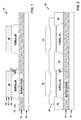
- FIG. 1 shows a lateral cross-section view of a CMOS device 10A including a self-aligned edge resistor 20 in mid-fabrication in a Shallow Trench Isolation (STI) partially depleted silicon on insulator (SOI) process, in one example.
- CMOS device 10A may be in a fabrication state as shown in FIG.
- an STI stack that includes a bulk silicon substrate 30, a buried oxide layer 32 or other type of buried insulator layer (e.g., a buried oxide layer of silicon dioxide) disposed on top of the bulk silicon substrate 30, a silicon device layer 34 disposed on top of the buried oxide layer 32, a pad oxide layer 40 disposed on top of the silicon device layer 34, an STI nitride barrier layer 42 disposed on top of the pad oxide layer 40, and a top oxide layer 48 disposed on top of the STI nitride barrier layer 42.
- a buried oxide layer 32 or other type of buried insulator layer e.g., a buried oxide layer of silicon dioxide
- CMOS device 10A As shown in FIG. 1 , the layers 30-48 of CMOS device 10A have been modified in CMOS STI process steps of patterning, etching, and initial doping, to eliminate portions of silicon device layer 34, pad oxide layer 40, STI nitride barrier layer 42, and top oxide layer 48 to create two silicon islands with first and second semiconductor wells, an n-type well 36 ("n-well 36") and a p-type well 38 ("p-well 38”) topped with STI nitride barrier blocks 44, 46 respectively.
- n-well 36 n-well 36
- p-well 38 p-type well 38
- the patterning and etching steps may include placement of a patterned photoresist mask over CMOS device 10A; etching via sputter, plasma, reactive-ion, or other etching technique; and stripping of the photoresist.
- N-well 36 may be doped with an n-type dopant (e.g., phosphorus) that donates electrons to surrounding silicon
- p-well 38 may be doped with a p-type dopant (e.g., boron) that donates electron holes to (i.e., that accepts electrons from) surrounding silicon.
- P-well 38 thus has opposite doping as N-well 36.
- CMOS device 10A as shown in FIG. 1 may provide electrical isolation between n-well 36 and p-well 38.
- a p-type dopant 22 (e.g., boron) is also implanted via a self-aligned, angled implantation into a compact internal sidewall edge area of n-well 36, resulting in a self-aligned edge resistor 20 along the compact internal sidewall edge area of n-well 36.
- the p-type dopant 22 of self-aligned edge resistor 20 inverts the doping of n-well 36 within the volume of self-aligned edge resistor 20.
- the implantation of p-type dopant 22 is self-aligned and angled around the implantation shadow of STI nitride barrier block 44.
- P-type dopant 22 may be implanted past and around the bulk of STI nitride barrier block 44 or other barrier, which prevents implantation of p-type dopant into the central body of n-well 36.
- Self-aligned edge resistor 20 is thus self-aligned along a compact, precisely controlled volume of the sidewall edge of n-well 36.
- any type of barrier layer may be used in place of STI nitride barrier layer 42 or STI nitride barrier block 44, and dopant ions may be implanted into the sidewall edge area of n-well 36 past the barrier shadow of the barrier layer.
- the p-type dopant 22 may also be incidentally implanted in the sidewall edge of p-well 38, though in this case, the p-type dopant will superimpose on the same p-type doping type as p-well 38 and not create an edge resistor in p-well 38.
- FIG. 2 shows a lateral cross-section view of a CMOS device 10B, corresponding to CMOS device 10A shown in FIG. 1 after additional process steps to deposit or otherwise form a Shallow Trench Isolation (STI) oxide layer 50 or other type of STI insulator layer, to planarize (chemically mechanically polish) STI oxide layer 50, to remove STI nitride barrier layer 42 (including STI nitride barrier blocks 44, 46), and to form a device gate layer 52, in one example.
- CMOS device 10B may thus include a transistor gate in device gate layer 52 over n-well 36 and p-well 38 with a self-aligned edge resistor 20 in the n-well 36.
- Device gate layer 52 may be formed by being deposited or thermally grown, in various examples.
- Self-aligned edge resistor 20 may thus connect a source and a drain (not shown in FIG. 2 ) self-aligned to device gate layer 52, in which the source and drain may also be n-type, as further described below.
- Self-aligned edge resistor 20 with p-type doping may thus enable the resistance between the source and drain to increase proportionally to source-to-drain bias.
- Buried oxide layer 32 and STI oxide layer 50 may thus electrically insulate and isolate n-well 36 and p-well 38 from each other and from other CMOS devices (not shown in FIG. 1 ) formed in the device layer 34, such as other similar n-well and p-well pairs.
- CMOS devices may be formed with an n-type self-aligned edge resistor along a silicon island sidewall edge in p-well 38.
- the process step of removing STI nitride barrier layer 42 (or other barrier layer) may include using a hot phosphoric strip, for example.
- p-type dopant 22 may be deposited via an ion implantation process.
- “implanting” may include any process for embedding, integrating, or depositing p-type dopant 22 into n-well 36.
- p-type dopant 22 may be deposited into the sidewall edge of n-well 36 to form self-aligned edge resistor 20 in multiple implant steps with repositioning of a wafer hosting CMOS device 10A/10B (collectively "CMOS device 10" between each implant step.
- CMOS device 10 CMOS device 10
- p-type dopant 22 may be divided into four equally divided portions to be implanted in four steps, and the wafer may be rotated 90 degrees between each implant step, a process known as quad mode implantation.
- this disclosure presents an STI SOI process to create a self-aligned edge resistor, a self-aligned edge resistor may be created using other types of isolation schemes or patterning and etching steps in other example processes.
- the height of the silicon islands formed by n-well 36 and p-well 38 may determine the width of the implantation of p-type dopant 22 in forming self-aligned edge resistor 20.
- the length of the implantation of p-type dopant 22 to form self-aligned edge resistor 20 may be controlled by the gate dimension which may be the most highly controlled dimension in a CMOS process.
- the depth of the implantation of p-type dopant 22 to form self-aligned edge resistor 20 may be controlled by implant variables which may also be highly controlled in a CMOS process.
- Self-aligned edge resistor 20 may thus be precisely formed with very compact size, very high resistance (e.g., approximately 100,000 to over a million ohms), and nominal read-write margin. Self-aligned edge resistor 20 may thus enable a small circuit architecture with reduction or prevention of SEU suitable for specialized applications such as space-based assets, and across a large temperature range and with low supply voltage.
- FIG. 3 shows lateral cross-section views of section views of various examples of CMOS devices 101, 102, 103, 104, 105, 106 ("CMOS devices 101-106") with respective self-aligned edge resistors 20A, 20B, 20C, 20D, 20E, 20F (collectively, "self-aligned edge resistors 20") implanted with different implant characteristics, in accordance with example two-dimensional simulations.
- CMOS devices 101-106 with respective self-aligned edge resistors 20A, 20B, 20C, 20D, 20E, 20F (collectively, "self-aligned edge resistors 20" implanted with different implant characteristics, in accordance with example two-dimensional simulations.
- CMOS devices 101-106 also have respective n-wells 36A, 36B, 36C, 36D, 36E, 36F (collectively, "n-wells 36") separated from respective self-aligned edge resistors 20A, 20B, 20C, 20D, 20E, 20F by respective inversion boundaries 21A, 21B, 21C, 21D, 21E, 21F.
- FIG. 3 shows sections of each of CMOS devices 101-106 with n-well 36 and self-aligned edge resistor 20 isolated by buried oxide layer 32 and STI oxide layer 50, and with gate layer 52 disposed above.
- Each of the six section views in FIG. 3 is a cross-sectional view of half of a gate, with a perspective in a direction between the source and the drain.
- self-aligned edge resistor 20 may be considered separate from the surrounding n-well 36 along a metallurgical junction where the n-type doping concentration of n-well 36 and the p-type doping concentration of self-aligned edge resistor 20 are balanced.
- FIG. 3 further shows how the different implant variables, in particular, implantation energies and doses in the examples of FIG. 3 , may determine the size, form, and doping concentration of the self-aligned edge resistors 20 in process simulations.
- CMOS device 102 shows a self-aligned edge resistor 20B with a higher implantation energy than self-aligned edge resistor 20A of CMOS device 101
- CMOS device 103 shows a self-aligned edge resistor 20C with a higher implantation energy than self-aligned edge resistor 20B of CMOS device 102.
- CMOS devices 101-103 show implantation energies of 20, 35, and 50 kilo-electronvolts (keV), respectively.
- the energy of implantation may be 10 keV or lower, or 100 keV or higher, depending on specific characteristics of a particular CMOS device, to enable sufficient current to flow through self-aligned edge resistor 20B for it to function as a transistor sidewall edge resistor.
- the resistance of self-aligned edge resistor 20B may thus form a conductive path between the source and the drain through a gate formed by CMOS device 102.
- the resistance of self-aligned edge resistor 20B may be sufficient to enable a current of a selected value to flow through the resistor when a gate bias of the gate is turned on, and a current of a lower value to flow through the resistor when the gate bias of the gate is turned off.
- the dopant may be implanted at a selected implantation dosage and a selected energy of implantation to provide the resistance sufficient to enable the current to flow through the resistor in this way.
- CMOS devices 104-106 show the same implantation energies as CMOS devices 101-103, respectively, but with a higher implantation dosage.
- CMOS devices 101-103 are all shown with an implantation dosage of 3x10 14 ions per square centimeter
- CMOS devices 104-106 are all shown with an implantation dosage of 5x10 14 ions per square centimeter.
- the selected implantation dosage may be 1x10 14 ions per square centimeter or lower, or 1x10 15 ions per square centimeter or higher, depending on the characteristics of the specific CMOS device to enable sufficient current to flow through self-aligned edge resistor 20B.
- the resistance value of self-aligned edge resistor 20 may be determined by the characteristics of the implant, such that the higher the implant dose, the lower the resistance.
- FIG. 4 shows an angled longitudinal/azimuthal cross-section view and cross-sectional views of another example CMOS device, labeled 111A in an angled longitudinal/azimuthal cross-section view (perpendicular to the views of FIGS. 1-3 ), and 111B in a lateral (as in FIGS. 1-3 ) cross-section view, respectively (collectively, "CMOS device 111"), with a self-aligned edge resistor 20G in an example three-dimensional simulation.
- View 111B is a lateral cross-section along vertical reference line 112A in view 111A.
- View 111A shows a lateral distribution of self-aligned edge resistor 20G relative to n-well 36, in one example.
- Self-aligned edge resistor 20G forms a p-type channel with a width of 0.34 micrometers (microns) in this example (and may have a larger or smaller width in other examples).
- Views 111A and 111B both indicate doping concentrations with dashed lines in approximately half-order of magnitude boundaries, such as from - 2.0 * 10 18 at right to + 1.2 * 10 18 at left in view 111B.
- CMOS device 111 in longitudinal/azimuthal view 111A shows a cross-section of an n-well 36 proximate an edge thereof and proximate the junction with self-aligned edge resistor 20G.
- CMOS device in perspective view 111A also shows STI oxide layer 50, and source and drain implants 62 and 64, respectively, on the top of the CMOS device, on either side of gate layer 52; and bulk silicon substrate 30.
- View 111B of CMOS device 111 shows lateral distribution of self-aligned edge resistor 20G relative to n-well 36 in silicon device layer 34, with gate layer 52 disposed above silicon device layer 34. View 111B also shows depletion region boundaries 19 and 23 within self-aligned edge resistor 20G and n-well 36, respectively, on either side of the inversion boundary 21 that defines the boundary between p-type self-aligned edge resistor 20G and n-well 36.
- Depletion region boundaries 19 and 23 as shown in view 111B are the edges of a depletion region between the n-type material in n-well 36 and the p-type material in self-aligned edge resistor 20G when a drain voltage V d of drain implant 64 and source voltage V s of source implant 62 are applied at -1.95 volts, and body voltage V body and gate voltage V gate are zero.
- the major part of the resistance of self-aligned edge resistor 20G in this example is due to the core part of self-aligned edge resistor 20G to the right of depletion region boundary 19 as shown in view 111B, which has a significantly higher ratio of p-type to n-type doping than within the depletion region portion of self-aligned edge resistor 20G between depletion region boundary 19 and inversion boundary 21.
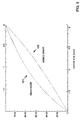
- FIG. 5 shows a graph of source to drain conductivity characteristics of self-aligned edge resistor 20G of FIG. 4 in a drain voltage sweep followed by a source voltage sweep, via drain implant 64 and source implant 62 on opposing sides of the transistor gate as shown in the angled longitudinal/azimuthal cross-section view 111A in FIG. 4 , in one example.
- the left y axis in FIG. 5 shows current from zero to 12 microamps
- the lower x axis shows the source voltage from -1.95 to 0 volts going from left to right
- the upper x axis shows the drain voltage from -1.95 to 0 volts going from right to left.
- Arc 121 shows a drain voltage sweep as drain voltage goes from 0 to -1.95 and current rises from 0 to 12 microamps
- arc 122 shows a subsequent source voltage sweep as source voltage goes from 0 to -1.95 and current drops back from 12 microamps to 0, while body voltage and gate voltage are 0.
- the graph of FIG. 5 shows that self-aligned edge resistor 20G remains conductive under all conditions, and that the source-drain voltage induces a sufficient depletion region to enable conduction through self-aligned edge resistor 20G.
- CMOS device 111 As CMOS device 111 is turned on and off, it can be driven into effective deep depletion equivalent to having a body tie bias on the device. CMOS device 111 is prevented from being turned off if a gate bias voltage or a body bias voltage appears.
- the effective resistance of self-aligned edge resistor 20G may vary proportionally to the source-to-drain bias voltage, and may be approximately in the range of 100,000 to ten million ohms.
- the effective resistance of self-aligned edge resistor 20G when drain-to-source bias voltage is near 0 may vary from about 90,000 to 200,000 ohms as a function of body bias, in this example. 200,000 ohms may occur in a worst case transient resistance in this example when the transistor is turned off and the body goes into deep depletion. In another example, the drain and source voltage may go to -1.2 volts instead of -1.95, and the worst case transient resistance effects may be smaller.
- FIG. 6 shows graphs 131, 132, 133, 134 of examples of current flowing through self-aligned edge resistor 20G as a function of drain voltage V drain in on and off gate bias conditions in three different example CMOS devices, in accordance with experimental results of measurements in example physical implementations of CMOS devices.
- Graphs 131 and 133 show current over voltage, in logarithmic and direct scales, respectively, in each of the three CMOS devices with a doping implantation density of 3x10 14 ions per square centimeter
- graphs 132 and 134 show current over voltage, also in logarithmic and direct scales, respectively, in each of the three CMOS devices with a doping implantation density of 5x10 14 ions per square centimeter.
- Graphs 131-134 all show current in microamps through self-aligned edge resistor 20G along the y axis, and applied drain voltage in volts along the x axis.
- Graphs 131 and 132 are in a logarithmic scale, while graphs 133 and 134 show a detailed section of interest of graphs 131 and 132, respectively, in a linear scale.
- the three different CMOS devices are a high voltage (HV), low voltage (LV), and super low voltage (SLV) versions, and the drain voltage V drain in each case rises from 0 to 1.2 volts.
- the HV version CMOS device may have a 3.3 volt transistor
- the LV version CMOS device may have a 1.8 volt transistor
- the SLV version CMOS device may have a 1.2 volt transistor, in these examples.
- self-aligned edge resistor 20G has a p-type channel with a width of 0.34 microns, as in the example of FIGS. 4 and 5 as described above.
- the current through self-aligned edge resistor 20G varies as voltage over resistance of self-aligned edge resistor 20G, where resistance varies proportionally to drain voltage, and is a function of the halo implantation dose of n-well 36 and the edge implantation dose of self-aligned edge resistor 20G, as shown in FIG. 4 .
- Self-aligned edge resistor 20G may achieve a resistance in the range of approximately 100,000 to one million ohms, in these examples.
- Self-aligned edge resistor 20G may have a p-type doping implantation level tuned to a specified resistance with respect to the voltage of the particular version of the CMOS device, with a relatively low doping level and relatively high resistance for the SLV version, a higher doping level and lower resistance for the LV version, and a still higher doping level and still lower resistance for the HV version.
- the implantation level of self-aligned edge resistor 20G may thus be adjusted relative to the voltage of the CMOS device version to target a specified resistance over the applicable voltage range.
- FIG. 7 depicts a flowchart for an example process 500 for forming a CMOS device with a self-aligned edge resistor, in accordance with illustrative aspects of this disclosure.
- process 500 includes implanting a dopant into a doped semiconductor well covered by a barrier, wherein the doped semiconductor well is disposed on a buried insulator and wherein the dopant is of opposite doping type to the doped semiconductor well, thereby forming a resistor on an edge of the doped semiconductor well, wherein the resistor has the opposite doping type (e.g., implanting a p-type dopant 22 such as boron into a sidewall edge of n-type doped semiconductor well 36 covered by the barrier of STI nitride barrier block 44 of STI nitride barrier layer 42 to form self-aligned edge resistor 20, wherein n-well 36 is disposed on the insulator of buried oxide layer 32, and wherein p-type dopant 22 is of
- Process 500 further includes forming a second insulator adjacent to the resistor (e.g., depositing an STI oxide layer 50 over CMOS device 10, including adjacent to self-aligned edge resistor 20) (504).
- Process 500 further includes removing the barrier (e.g., removing STI nitride barrier block 44) (506).
- Process 500 further includes forming a gate layer on the doped semiconductor well, thereby forming a gate adjacent to the doped semiconductor well and the resistor (e.g., depositing or thermally growing gate layer 52 on CMOS device 10 including n-well 36) (508).
- a self-aligned edge resistor as described herein may be particularly advantageous in radiation hardened circuits, in some examples. Such circuits may use a self-aligned edge resistor as described herein to mitigate ion induced glitching, state changes, or other failure modes. However, it is also contemplated that a self-aligned edge resistor as described herein may also be used where appropriate in various other applications not involving radiation hardened requirements.
- the term "deposited” may generically refer to Chemical Vapor Deposition (CVD), plasma enhanced CVD, and other methods of fabricating dielectric or other semiconductor related films.
Landscapes
- Metal-Oxide And Bipolar Metal-Oxide Semiconductor Integrated Circuits (AREA)
- Semiconductor Memories (AREA)
- Thin Film Transistor (AREA)
Abstract
Description
- This disclosure relates to complementary metal-oxide-semiconductor (CMOS) integrated circuits, and more particularly, to CMOS integrated circuit electronic circuits fabricated in a partially depleted silicon on insulator (SOI) process.
- Some CMOS integrated circuits may be made in a partially depleted silicon on insulator (SOI) process. Certain applications such as electronics for satellites, upper rocket stages, space probes, spaceships, and other applications with radiation-hardened requirements impose special demands such as single event upset (SEU) mitigation, or mitigating electronic state upsets by single radiation-induced events, that are not met by circuit architecture for ordinary consumer electronics. SEU in space is caused by energetic particles traversing circuit nodes and depositing charge sufficient to disrupt operation.
- Space applications typically call for random access memory (RAM) with high performance and low power requirements, as well as protection against radiation effects. Radiation can cause many undesirable effects in circuit operation. For example, radiation can change the conductance of MOS transistors by changing the threshold voltage (Vt). In space, heavy particles from a single cosmic ray are capable of depositing relatively large amounts of deposited charge on a circuit node. There is a direct relationship between the radiation induced upset rate requirements and the performance requirement of radiation hardened static random access memory (SRAM). Radiation can also generate significant levels of transient voltage and current disturbances on internal nodes, including power and ground.
- These internal disturbances can slow circuit performance or even upset circuit operation, e.g., changing the state of a memory cell. For a given node within a memory cell, there exists an amount of deposited charge which the driving transistor and the nodal capacitance cannot absorb without failing to maintain the node in the desired state. Therefore, the radiation induced charge can result in a change in the stored data state. Some specialized circuit architecture technologies have used designs such as back-to-back reverse-biased Schottky resistors as compact high value resistors with an active delay element (ADE) in SRAM cells.
- This disclosure is directed to techniques, methods, and systems for fabricating SRAM cells with resistors formed along the sidewall edges of transistors (e.g., ADE transistors) by self-aligned, angled implantation, which may enable more compact SRAM architecture with SEU mitigation. The implantation is done prior to removal of a Shallow Trench Isolation (STI) barrier such as nitride, enabling the implantation to be self-aligned to the sidewall edge of the silicon island. The height of the silicon islands may determine the width of the implantation. The length of the implantation may be controlled by the gate dimension which may be the most highly controlled dimension in a CMOS process. The depth of the implantation may be controlled by implant variables which may also be highly controlled in a CMOS process. A self-aligned transistor sidewall edge resistor of this disclosure may thus be precisely formed with very compact size, very high resistance (e.g., approximately 100,000 to over a million ohms), and nominal read-write margin. A self-aligned transistor sidewall edge resistor of this disclosure may thus enable a small circuit architecture with reduction or prevention of SEU suitable for specialized applications such as space-based assets, and across a large temperature range and with low supply voltage.
- In one example, a complementary metal-oxide semiconductor (CMOS) device includes a first semiconductor well disposed on a first insulator, the first semiconductor well having a first doping type. The CMOS device further includes a second insulator disposed in the first semiconductor well. The CMOS device further includes a gate disposed on the first semiconductor well. The CMOS device further includes a resistor disposed on an edge of the first doped semiconductor well, adjacent to the second insulator and in contact with the gate, the resistor having a second doping type opposite the first doping type.
- In another example, a method includes implanting a dopant into a doped semiconductor well covered by a barrier, wherein the doped semiconductor well is disposed on a buried insulator and wherein the dopant is of opposite doping type to the doped semiconductor well, thereby forming a resistor on an edge of the doped semiconductor well, wherein the resistor has the opposite doping type. The method further includes forming a second insulator adjacent to the resistor, removing the barrier, and forming a gate layer on the doped semiconductor well, thereby forming a gate adjacent to the doped semiconductor well and the resistor.
- The details of one or more examples are set forth in the accompanying drawings and the description below. Other features, objects, and advantages will be apparent from the description and drawings, and from the claims.
-
-
FIG. 1 shows a lateral cross-section view of a CMOS device including a self-aligned edge resistor in mid-fabrication in a Shallow Trench Isolation (STI) partially depleted silicon on insulator (SOI) process, in one example. -
FIG. 2 shows a lateral cross-section view of a CMOS device corresponding to the CMOS device shown inFIG. 1 after additional process steps to deposit an STI oxide layer, to planarize the STI oxide layer, to remove the STI nitride barrier layer, and to deposit a device gate layer, in one example. -
FIG. 3 shows lateral cross-section views of various examples of CMOS devices with respective self-aligned edge resistors implanted with different implant characteristics, in accordance with example two-dimensional simulations. -
FIG. 4 shows an angled longitudinal/azimuthal cross-section view and lateral cross-section views of another example CMOS device with a self-aligned edge resistor in an example three-dimensional simulation. -
FIG. 5 shows a graph of source to drain conductivity characteristics of the self-aligned edge resistor ofFIG. 4 in a drain voltage sweep followed by a source voltage sweep, via a drain implant and source implant on opposing sides of the transistor gate as shown in the angled longitudinal/azimuthal cross-section view inFIG. 4 , in one example. -
FIG. 6 shows graphs of examples of current flowing through a self-aligned edge resistor as a function of drain voltage in on and off gate bias conditions in three different example CMOS devices, in accordance with experimental results of measurements in example physical implementations of CMOS devices. -
FIG. 7 depicts a flowchart for an example process for forming a CMOS device with a self-aligned edge resistor, in accordance with illustrative aspects of this disclosure. - Various examples are described below directed to techniques, methods, systems, and devices for fabricating SRAM cells with resistors formed along the sidewall edges of transistors (e.g., ADE transistors) by self-aligned, angled implantation. A self-aligned SRAM cell sidewall edge resistor ("self-aligned edge resistor") as described herein may minimize effects of turning the transistor off on the resistor value, while enabling the resistance to increase proportionally to source-to-drain bias. In addition, the gate to source/drain capacitance may be reduced by a factor of two or more relative to typical SRAM cells using Schottky elements, since the extra capacitance associated with the gate next to the Schottky elements is eliminated. The dimensions of the self-aligned edge resistor may be controlled by the thickness of the starting top silicon layer on the SOI substrate and the gate masking step, which may be the most highly controlled dimensions in an SOI CMOS process, resulting in the ability to control the resistor value to a high degree of precision relative to previous techniques. The improvement in both control and temperature stability enabled by the self-aligned edge resistor may be sufficient to avoid a requirement to turn on the transistor during the read/write cycle, as is typical in previous techniques, thus further minimizing circuit design complexity.
- A self-aligned edge resistor as described herein may be compatible with the minimum-sized transistor available in the technology, and may be compatible with either a p-channel or n-channel transistor, permitting optimization for SRAM cell size. For example, a p-channel option (a p-type edge implant in an n-type well) for implementing a self-aligned edge resistor may maximize usable resistance for a given doping level due to approximately three times lower mobility and may balance n-well and p-well area to maximize density.
- The high degree of control for the dimensions of the self-aligned edge resistor may be an advantage over other planar resistor solutions, and the use of an SOI silicon process may provide improved control and temperature effects over polysilicon processes. A self-aligned edge resistor may increase resistance with source-to-drain bias which may enable excellent resistor characteristics even when the transistor part is turned off. A self-aligned edge resistor may also scale down with successively smaller technology generations, and may directly enable smaller SRAM area using smaller values of active power. A self-aligned edge resistor may also enable advantageous implementations in any application requiring a compact resistor with high-precision, high resistance value, including in analog circuits.
-
FIG. 1 shows a lateral cross-section view of a CMOS device 10A including a self-alignededge resistor 20 in mid-fabrication in a Shallow Trench Isolation (STI) partially depleted silicon on insulator (SOI) process, in one example. CMOS device 10A may be in a fabrication state as shown inFIG. 1 after initial process functions performed on an STI stack that includes abulk silicon substrate 30, a buriedoxide layer 32 or other type of buried insulator layer (e.g., a buried oxide layer of silicon dioxide) disposed on top of thebulk silicon substrate 30, asilicon device layer 34 disposed on top of the buriedoxide layer 32, apad oxide layer 40 disposed on top of thesilicon device layer 34, an STI nitride barrier layer 42 disposed on top of thepad oxide layer 40, and a top oxide layer 48 disposed on top of the STI nitride barrier layer 42. - As shown in
FIG. 1 , the layers 30-48 of CMOS device 10A have been modified in CMOS STI process steps of patterning, etching, and initial doping, to eliminate portions ofsilicon device layer 34,pad oxide layer 40, STI nitride barrier layer 42, and top oxide layer 48 to create two silicon islands with first and second semiconductor wells, an n-type well 36 ("n-well 36") and a p-type well 38 ("p-well 38") topped with STInitride barrier blocks well 38 may be doped with a p-type dopant (e.g., boron) that donates electron holes to (i.e., that accepts electrons from) surrounding silicon. P-well 38 thus has opposite doping as N-well 36. CMOS device 10A as shown inFIG. 1 may provide electrical isolation between n-well 36 and p-well 38. - In CMOS device 10A as shown in
FIG. 1 , a p-type dopant 22 (e.g., boron) is also implanted via a self-aligned, angled implantation into a compact internal sidewall edge area of n-well 36, resulting in a self-alignededge resistor 20 along the compact internal sidewall edge area of n-well 36. The p-type dopant 22 of self-alignededge resistor 20 inverts the doping of n-well 36 within the volume of self-alignededge resistor 20. The implantation of p-type dopant 22 is self-aligned and angled around the implantation shadow of STInitride barrier block 44. P-type dopant 22 may be implanted past and around the bulk of STInitride barrier block 44 or other barrier, which prevents implantation of p-type dopant into the central body of n-well 36. Self-alignededge resistor 20 is thus self-aligned along a compact, precisely controlled volume of the sidewall edge of n-well 36. - In other examples, any type of barrier layer may be used in place of STI nitride barrier layer 42 or STI
nitride barrier block 44, and dopant ions may be implanted into the sidewall edge area of n-well 36 past the barrier shadow of the barrier layer. Depending on the dopant implant technique, the p-type dopant 22 may also be incidentally implanted in the sidewall edge of p-well 38, though in this case, the p-type dopant will superimpose on the same p-type doping type as p-well 38 and not create an edge resistor in p-well 38. -
FIG. 2 shows a lateral cross-section view of a CMOS device 10B, corresponding to CMOS device 10A shown inFIG. 1 after additional process steps to deposit or otherwise form a Shallow Trench Isolation (STI)oxide layer 50 or other type of STI insulator layer, to planarize (chemically mechanically polish)STI oxide layer 50, to remove STI nitride barrier layer 42 (including STI nitride barrier blocks 44, 46), and to form adevice gate layer 52, in one example. CMOS device 10B may thus include a transistor gate indevice gate layer 52 over n-well 36 and p-well 38 with a self-alignededge resistor 20 in the n-well 36.Device gate layer 52 may be formed by being deposited or thermally grown, in various examples. Self-alignededge resistor 20 may thus connect a source and a drain (not shown inFIG. 2 ) self-aligned todevice gate layer 52, in which the source and drain may also be n-type, as further described below. Self-alignededge resistor 20 with p-type doping may thus enable the resistance between the source and drain to increase proportionally to source-to-drain bias. -
Buried oxide layer 32 andSTI oxide layer 50 may thus electrically insulate and isolate n-well 36 and p-well 38 from each other and from other CMOS devices (not shown inFIG. 1 ) formed in thedevice layer 34, such as other similar n-well and p-well pairs. In other examples, a CMOS device may be formed with an n-type self-aligned edge resistor along a silicon island sidewall edge in p-well 38. The process step of removing STI nitride barrier layer 42 (or other barrier layer) may include using a hot phosphoric strip, for example. - In some examples, p-
type dopant 22 may be deposited via an ion implantation process. In various examples, "implanting" may include any process for embedding, integrating, or depositing p-type dopant 22 into n-well 36. In some examples, p-type dopant 22 may be deposited into the sidewall edge of n-well 36 to form self-alignededge resistor 20 in multiple implant steps with repositioning of a wafer hosting CMOS device 10A/10B (collectively "CMOS device 10") between each implant step. For example, p-type dopant 22 may be divided into four equally divided portions to be implanted in four steps, and the wafer may be rotated 90 degrees between each implant step, a process known as quad mode implantation. Although this disclosure presents an STI SOI process to create a self-aligned edge resistor, a self-aligned edge resistor may be created using other types of isolation schemes or patterning and etching steps in other example processes. - Thus, the height of the silicon islands formed by n-well 36 and p-well 38 may determine the width of the implantation of p-
type dopant 22 in forming self-alignededge resistor 20. The length of the implantation of p-type dopant 22 to form self-alignededge resistor 20 may be controlled by the gate dimension which may be the most highly controlled dimension in a CMOS process. The depth of the implantation of p-type dopant 22 to form self-alignededge resistor 20 may be controlled by implant variables which may also be highly controlled in a CMOS process. Self-alignededge resistor 20 may thus be precisely formed with very compact size, very high resistance (e.g., approximately 100,000 to over a million ohms), and nominal read-write margin. Self-alignededge resistor 20 may thus enable a small circuit architecture with reduction or prevention of SEU suitable for specialized applications such as space-based assets, and across a large temperature range and with low supply voltage. -
FIG. 3 shows lateral cross-section views of section views of various examples ofCMOS devices edge resistors edge resistors 20") implanted with different implant characteristics, in accordance with example two-dimensional simulations. CMOS devices 101-106 also have respective n-wells wells 36") separated from respective self-alignededge resistors respective inversion boundaries FIG. 3 shows sections of each of CMOS devices 101-106 with n-well 36 and self-alignededge resistor 20 isolated byburied oxide layer 32 andSTI oxide layer 50, and withgate layer 52 disposed above. Each of the six section views inFIG. 3 is a cross-sectional view of half of a gate, with a perspective in a direction between the source and the drain. In each case, self-alignededge resistor 20 may be considered separate from the surrounding n-well 36 along a metallurgical junction where the n-type doping concentration of n-well 36 and the p-type doping concentration of self-alignededge resistor 20 are balanced. -
FIG. 3 further shows how the different implant variables, in particular, implantation energies and doses in the examples ofFIG. 3 , may determine the size, form, and doping concentration of the self-alignededge resistors 20 in process simulations. In particular,CMOS device 102 shows a self-alignededge resistor 20B with a higher implantation energy than self-alignededge resistor 20A ofCMOS device 101, andCMOS device 103 shows a self-alignededge resistor 20C with a higher implantation energy than self-alignededge resistor 20B ofCMOS device 102. In the particular examples shown, CMOS devices 101-103 show implantation energies of 20, 35, and 50 kilo-electronvolts (keV), respectively. In other examples, the energy of implantation may be 10 keV or lower, or 100 keV or higher, depending on specific characteristics of a particular CMOS device, to enable sufficient current to flow through self-alignededge resistor 20B for it to function as a transistor sidewall edge resistor. - The resistance of self-aligned
edge resistor 20B may thus form a conductive path between the source and the drain through a gate formed byCMOS device 102. The resistance of self-alignededge resistor 20B may be sufficient to enable a current of a selected value to flow through the resistor when a gate bias of the gate is turned on, and a current of a lower value to flow through the resistor when the gate bias of the gate is turned off. The dopant may be implanted at a selected implantation dosage and a selected energy of implantation to provide the resistance sufficient to enable the current to flow through the resistor in this way. - CMOS devices 104-106 show the same implantation energies as CMOS devices 101-103, respectively, but with a higher implantation dosage. In particular, CMOS devices 101-103 are all shown with an implantation dosage of 3x10¹⁴ ions per square centimeter, while CMOS devices 104-106 are all shown with an implantation dosage of 5x10¹⁴ ions per square centimeter. In other examples, the selected implantation dosage may be 1x10¹⁴ ions per square centimeter or lower, or 1x10¹⁵ ions per square centimeter or higher, depending on the characteristics of the specific CMOS device to enable sufficient current to flow through self-aligned
edge resistor 20B. The resistance value of self-alignededge resistor 20 may be determined by the characteristics of the implant, such that the higher the implant dose, the lower the resistance. -
FIG. 4 shows an angled longitudinal/azimuthal cross-section view and cross-sectional views of another example CMOS device, labeled 111A in an angled longitudinal/azimuthal cross-section view (perpendicular to the views ofFIGS. 1-3 ), and 111B in a lateral (as inFIGS. 1-3 ) cross-section view, respectively (collectively, "CMOS device 111"), with a self-alignededge resistor 20G in an example three-dimensional simulation.View 111B is a lateral cross-section alongvertical reference line 112A inview 111A.View 111A shows a lateral distribution of self-alignededge resistor 20G relative to n-well 36, in one example. Self-alignededge resistor 20G forms a p-type channel with a width of 0.34 micrometers (microns) in this example (and may have a larger or smaller width in other examples).Views view 111B. CMOS device 111 in longitudinal/azimuthal view 111A shows a cross-section of an n-well 36 proximate an edge thereof and proximate the junction with self-alignededge resistor 20G. CMOS device inperspective view 111A also showsSTI oxide layer 50, and source and drainimplants gate layer 52; andbulk silicon substrate 30. -
View 111B of CMOS device 111 shows lateral distribution of self-alignededge resistor 20G relative to n-well 36 insilicon device layer 34, withgate layer 52 disposed abovesilicon device layer 34.View 111B also showsdepletion region boundaries edge resistor 20G and n-well 36, respectively, on either side of theinversion boundary 21 that defines the boundary between p-type self-alignededge resistor 20G and n-well 36.Depletion region boundaries view 111B are the edges of a depletion region between the n-type material in n-well 36 and the p-type material in self-alignededge resistor 20G when a drain voltage Vd ofdrain implant 64 and source voltage Vs ofsource implant 62 are applied at -1.95 volts, and body voltage Vbody and gate voltage Vgate are zero. The major part of the resistance of self-alignededge resistor 20G in this example is due to the core part of self-alignededge resistor 20G to the right ofdepletion region boundary 19 as shown inview 111B, which has a significantly higher ratio of p-type to n-type doping than within the depletion region portion of self-alignededge resistor 20G betweendepletion region boundary 19 andinversion boundary 21. -
FIG. 5 shows a graph of source to drain conductivity characteristics of self-alignededge resistor 20G ofFIG. 4 in a drain voltage sweep followed by a source voltage sweep, viadrain implant 64 and source implant 62 on opposing sides of the transistor gate as shown in the angled longitudinal/azimuthal cross-section view 111A inFIG. 4 , in one example. The left y axis inFIG. 5 shows current from zero to 12 microamps, the lower x axis shows the source voltage from -1.95 to 0 volts going from left to right, and the upper x axis shows the drain voltage from -1.95 to 0 volts going from right to left.Arc 121 shows a drain voltage sweep as drain voltage goes from 0 to -1.95 and current rises from 0 to 12 microamps, andarc 122 shows a subsequent source voltage sweep as source voltage goes from 0 to -1.95 and current drops back from 12 microamps to 0, while body voltage and gate voltage are 0. - The graph of
FIG. 5 shows that self-alignededge resistor 20G remains conductive under all conditions, and that the source-drain voltage induces a sufficient depletion region to enable conduction through self-alignededge resistor 20G. As CMOS device 111 is turned on and off, it can be driven into effective deep depletion equivalent to having a body tie bias on the device. CMOS device 111 is prevented from being turned off if a gate bias voltage or a body bias voltage appears. The effective resistance of self-alignededge resistor 20G may vary proportionally to the source-to-drain bias voltage, and may be approximately in the range of 100,000 to ten million ohms. The effective resistance of self-alignededge resistor 20G when drain-to-source bias voltage is near 0 may vary from about 90,000 to 200,000 ohms as a function of body bias, in this example. 200,000 ohms may occur in a worst case transient resistance in this example when the transistor is turned off and the body goes into deep depletion. In another example, the drain and source voltage may go to -1.2 volts instead of -1.95, and the worst case transient resistance effects may be smaller. -
FIG. 6 showsgraphs edge resistor 20G as a function of drain voltage Vdrain in on and off gate bias conditions in three different example CMOS devices, in accordance with experimental results of measurements in example physical implementations of CMOS devices.Graphs graphs edge resistor 20G along the y axis, and applied drain voltage in volts along the x axis.Graphs graphs graphs - The three different CMOS devices are a high voltage (HV), low voltage (LV), and super low voltage (SLV) versions, and the drain voltage Vdrain in each case rises from 0 to 1.2 volts. The HV version CMOS device may have a 3.3 volt transistor, the LV version CMOS device may have a 1.8 volt transistor, and the SLV version CMOS device may have a 1.2 volt transistor, in these examples.
- In each example, self-aligned
edge resistor 20G has a p-type channel with a width of 0.34 microns, as in the example ofFIGS. 4 and5 as described above. The current through self-alignededge resistor 20G varies as voltage over resistance of self-alignededge resistor 20G, where resistance varies proportionally to drain voltage, and is a function of the halo implantation dose of n-well 36 and the edge implantation dose of self-alignededge resistor 20G, as shown inFIG. 4 . Self-alignededge resistor 20G may achieve a resistance in the range of approximately 100,000 to one million ohms, in these examples. Self-alignededge resistor 20G may have a p-type doping implantation level tuned to a specified resistance with respect to the voltage of the particular version of the CMOS device, with a relatively low doping level and relatively high resistance for the SLV version, a higher doping level and lower resistance for the LV version, and a still higher doping level and still lower resistance for the HV version. The implantation level of self-alignededge resistor 20G may thus be adjusted relative to the voltage of the CMOS device version to target a specified resistance over the applicable voltage range. While this example is discussed in terms of forming self-alignededge resistor 20G with a p-type dopant implanted into the sidewall edge of an n-type well, other examples may be implemented with a self-aligned edge resistor formed of an n-type doping implantation into an edge of a p-type well. - In graphs 131-134, the higher values of current occur in the drain voltage Vdrain on condition, when the drain voltage in the CMOS device is applied or turned on. In this condition, the current shorts out self-aligned
edge resistor 20G. When the drain voltage is turned off, the resistance remains, and at a high value. Self-alignededge resistor 20G thus enables voltage still to be applied to the body of the CMOS device when the drain voltage of the CMOS device is turned off. Self-alignededge resistor 20G may thus also prevent floating body effects in the CMOS device and mitigate the risk of an SEU in an SRAM cell that includes the CMOS device. -
FIG. 7 depicts a flowchart for anexample process 500 for forming a CMOS device with a self-aligned edge resistor, in accordance with illustrative aspects of this disclosure. In this example,process 500 includes implanting a dopant into a doped semiconductor well covered by a barrier, wherein the doped semiconductor well is disposed on a buried insulator and wherein the dopant is of opposite doping type to the doped semiconductor well, thereby forming a resistor on an edge of the doped semiconductor well, wherein the resistor has the opposite doping type (e.g., implanting a p-type dopant 22 such as boron into a sidewall edge of n-type doped semiconductor well 36 covered by the barrier of STInitride barrier block 44 of STI nitride barrier layer 42 to form self-alignededge resistor 20, wherein n-well 36 is disposed on the insulator of buriedoxide layer 32, and wherein p-type dopant 22 is of opposite doping type to n-type well 36, as described above) (502).Process 500 further includes forming a second insulator adjacent to the resistor (e.g., depositing anSTI oxide layer 50 overCMOS device 10, including adjacent to self-aligned edge resistor 20) (504).Process 500 further includes removing the barrier (e.g., removing STI nitride barrier block 44) (506).Process 500 further includes forming a gate layer on the doped semiconductor well, thereby forming a gate adjacent to the doped semiconductor well and the resistor (e.g., depositing or thermally growinggate layer 52 onCMOS device 10 including n-well 36) (508). - Although various example methods are described above with reference to an STI scheme in an SOI process, other examples may be carried out at other points of an SOI process. A self-aligned edge resistor as described herein may be particularly advantageous in radiation hardened circuits, in some examples. Such circuits may use a self-aligned edge resistor as described herein to mitigate ion induced glitching, state changes, or other failure modes. However, it is also contemplated that a self-aligned edge resistor as described herein may also be used where appropriate in various other applications not involving radiation hardened requirements. The term "deposited" may generically refer to Chemical Vapor Deposition (CVD), plasma enhanced CVD, and other methods of fabricating dielectric or other semiconductor related films.
- Various aspects of the disclosure have been described. These and other aspects are within the scope of the following claims.
Claims (10)
- A complementary metal-oxide semiconductor (CMOS) device (12, 101, 102, 103, 104, 105, 106, 111) comprising:a first semiconductor well (36) disposed on a first insulator (32), the first semiconductor well having a first doping type;a second insulator (50) disposed in the first semiconductor well;a gate (52) disposed on the first semiconductor well; anda resistor (20) disposed on an edge of the first doped semiconductor well, adjacent to the second insulator and in contact with the gate, the resistor having a second doping type opposite the first doping type.
- The CMOS device of claim 1, wherein the resistor is implanted (22) in the edge of the first doped semiconductor well.
- The CMOS device of claim 1, wherein the first doping type is doped with an n-type dopant, and the opposing second doping type is doped with a p-type dopant.
- The CMOS device of claim 1, wherein the resistor is doped with an implantation dosage selected from a range of approximately 1x10¹⁴ to 1x10¹⁵ ions per square centimeter.
- The CMOS device of claim 1, wherein the resistor enables a current to flow through a source and a drain of the gate through the resistor, wherein the resistance of the resistor is sufficient to enable a first current to flow through the resistor when a gate bias of the gate is turned on, and a second current to flow through the resistor when the gate bias of the gate is turned off, wherein the second current is lower than the first current.
- The CMOS device of claim 1, wherein the resistance of the resistor varies proportionally to a current through the resistor.
- The CMOS device of claim 1, further comprising a second semiconductor well (38) disposed on the buried insulator, wherein the second semiconductor well has opposite doping as the first semiconductor well.
- A method (500) comprising:implanting (502, 22) a dopant (20) into a doped semiconductor well (36) covered by a barrier (44, 40, 42, 48), wherein the doped semiconductor well is disposed on a buried insulator (32) and wherein the dopant is of opposite doping type to the doped semiconductor well, thereby forming a resistor (20) on an edge of the doped semiconductor well, wherein the resistor has the opposite doping type;forming (504) a second insulator (50) adjacent to the resistor;removing (506) the barrier; andforming (508) a gate layer (52) on the doped semiconductor well, thereby forming a gate (52) adjacent to the doped semiconductor well and the resistor.
- The method of claim 8, wherein implanting the dopant into the doped semiconductor well comprises implanting the dopant at a selected implantation dosage and a selected energy of implantation to provide a resistance sufficient to enable a current to flow through the resistor,
wherein implanting the dopant into the doped semiconductor well further comprises implanting the dopant at the selected implantation dosage and the selected energy of implantation such that the resistance is sufficient to enable a first current to flow through the resistor when a gate bias of the gate is turned on, and a second current to flow through the resistor when the gate bias of the gate is turned off, where the second current is lower than the first current. - The method of claim 8, wherein the doped semiconductor well comprises an n-type well doped with phosphorus, and the dopant implanted to form the resistor comprises a p-type dopant, wherein the p-type dopant comprises boron, the method further comprising:forming a source and a drain self-aligned to the gate layer, such that the resistor on the edge of the doped semiconductor well provides a conductive path between the source and the drain.
Applications Claiming Priority (1)
| Application Number | Priority Date | Filing Date | Title |
|---|---|---|---|
| US14/705,778 US9773808B2 (en) | 2015-05-06 | 2015-05-06 | Compact self-aligned implantation transistor edge resistor for SRAM SEU mitigation |
Publications (2)
| Publication Number | Publication Date |
|---|---|
| EP3091574A1 true EP3091574A1 (en) | 2016-11-09 |
| EP3091574B1 EP3091574B1 (en) | 2025-03-12 |
Family
ID=55808437
Family Applications (1)
| Application Number | Title | Priority Date | Filing Date |
|---|---|---|---|
| EP16166509.6A Active EP3091574B1 (en) | 2015-05-06 | 2016-04-21 | Compact self-aligned implantation transistor edge resistor for sram seu mitigation |
Country Status (3)
| Country | Link |
|---|---|
| US (1) | US9773808B2 (en) |
| EP (1) | EP3091574B1 (en) |
| JP (1) | JP6746365B2 (en) |
Families Citing this family (1)
| Publication number | Priority date | Publication date | Assignee | Title |
|---|---|---|---|---|
| US10636876B2 (en) * | 2018-07-26 | 2020-04-28 | Globalfoundries Inc. | Devices with channel extension regions |
Citations (4)
| Publication number | Priority date | Publication date | Assignee | Title |
|---|---|---|---|---|
| US4212683A (en) * | 1978-03-27 | 1980-07-15 | Ncr Corporation | Method for making narrow channel FET |
| US5053345A (en) * | 1989-02-06 | 1991-10-01 | Harris Corporation | Method of edge doping SOI islands |
| US5206533A (en) * | 1991-06-24 | 1993-04-27 | Texas Instruments Incorporated | Transistor device with resistive coupling |
| US20110207281A1 (en) * | 2010-02-22 | 2011-08-25 | Kamoshita Junichi | Semiconductor device and method of producing semiconductor device |
Family Cites Families (14)
| Publication number | Priority date | Publication date | Assignee | Title |
|---|---|---|---|---|
| JPS5558575A (en) * | 1978-10-26 | 1980-05-01 | Fujitsu Ltd | Semiconductor device |
| JPS57106234A (en) * | 1980-12-24 | 1982-07-02 | Fujitsu Ltd | Logical operation circuit |
| US5241211A (en) | 1989-12-20 | 1993-08-31 | Nec Corporation | Semiconductor device |
| US5631863A (en) | 1995-02-14 | 1997-05-20 | Honeywell Inc. | Random access memory cell resistant to radiation induced upsets |
| US5665629A (en) | 1995-08-11 | 1997-09-09 | International Business Machines Corporation | Four transistor SRAM process |
| US5578854A (en) | 1995-08-11 | 1996-11-26 | International Business Machines Corporation | Vertical load resistor SRAM cell |
| US7486541B2 (en) | 2003-06-13 | 2009-02-03 | Taiwan Semiconductor Manufacturing Company, Ltd. | Resistive cell structure for reducing soft error rate |
| US7200031B2 (en) | 2005-03-16 | 2007-04-03 | Honeywell International, Inc. | Proton and heavy ion SEU resistant SRAM |
| US7375000B2 (en) | 2005-08-22 | 2008-05-20 | International Business Machines Corporation | Discrete on-chip SOI resistors |
| US7361959B2 (en) * | 2005-11-28 | 2008-04-22 | International Business Machines Corporation | CMOS circuits including a passive element having a low end resistance |
| US7732287B2 (en) | 2006-05-02 | 2010-06-08 | Honeywell International Inc. | Method of forming a body-tie |
| US7965540B2 (en) | 2008-03-26 | 2011-06-21 | International Business Machines Corporation | Structure and method for improving storage latch susceptibility to single event upsets |
| US20100117153A1 (en) * | 2008-11-07 | 2010-05-13 | Honeywell International Inc. | High voltage soi cmos device and method of manufacture |
| JP5525249B2 (en) * | 2009-12-08 | 2014-06-18 | ラピスセミコンダクタ株式会社 | Semiconductor device and manufacturing method thereof |
-
2015
- 2015-05-06 US US14/705,778 patent/US9773808B2/en active Active
-
2016
- 2016-04-21 EP EP16166509.6A patent/EP3091574B1/en active Active
- 2016-04-28 JP JP2016090129A patent/JP6746365B2/en active Active
Patent Citations (4)
| Publication number | Priority date | Publication date | Assignee | Title |
|---|---|---|---|---|
| US4212683A (en) * | 1978-03-27 | 1980-07-15 | Ncr Corporation | Method for making narrow channel FET |
| US5053345A (en) * | 1989-02-06 | 1991-10-01 | Harris Corporation | Method of edge doping SOI islands |
| US5206533A (en) * | 1991-06-24 | 1993-04-27 | Texas Instruments Incorporated | Transistor device with resistive coupling |
| US20110207281A1 (en) * | 2010-02-22 | 2011-08-25 | Kamoshita Junichi | Semiconductor device and method of producing semiconductor device |
Also Published As
| Publication number | Publication date |
|---|---|
| EP3091574B1 (en) | 2025-03-12 |
| JP2017022362A (en) | 2017-01-26 |
| JP6746365B2 (en) | 2020-08-26 |
| US20160329349A1 (en) | 2016-11-10 |
| US9773808B2 (en) | 2017-09-26 |
Similar Documents
| Publication | Publication Date | Title |
|---|---|---|
| US8252642B2 (en) | Fabrication methods for radiation hardened isolation structures | |
| KR101194973B1 (en) | Transistor of semiconductor device and method of forming the same | |
| US8552500B2 (en) | Structure for CMOS ETSOI with multiple threshold voltages and active well bias capability | |
| US8093107B1 (en) | Thyristor semiconductor memory and method of manufacture | |
| JP2965783B2 (en) | Semiconductor device and manufacturing method thereof | |
| US9570465B2 (en) | Dual STI integrated circuit including FDSOI transistors and method for manufacturing the same | |
| CN107425057A (en) | Semiconductor structure of transistor including being provided with gate electrode area in the substrate and forming method thereof | |
| US20160013206A1 (en) | Low leakage dual sti integrated circuit including fdsoi transistors | |
| US10217838B2 (en) | Semiconductor structure with multiple transistors having various threshold voltages | |
| US6730555B2 (en) | Transistors having selectively doped channel regions | |
| TW201822361A (en) | MOS capacitor structure for reducing capacitance variability | |
| US6847065B1 (en) | Radiation-hardened transistor fabricated by modified CMOS process | |
| US9773808B2 (en) | Compact self-aligned implantation transistor edge resistor for SRAM SEU mitigation | |
| WO2005104209A1 (en) | Methods for forming super-steep diffusion region profiles in mos devices and resulting semiconductor topographies | |
| US9536880B2 (en) | Devices having multiple threshold voltages and method of fabricating such devices | |
| US20200295004A1 (en) | Cmos-based integrated circuit products with isolated p-wells for body-biasing transistor devices | |
| US5939757A (en) | Semiconductor device having triple well structure | |
| US5917247A (en) | Static type memory cell structure with parasitic capacitor | |
| US6326247B1 (en) | Method of creating selectively thin silicon/oxide for making fully and partially depleted SOI on same waffer | |
| US20100244145A1 (en) | Semiconductor memory device using hot electron injection | |
| Cham et al. | A study of the trench surface inversion problem in the trench CMOS technology | |
| US7588991B2 (en) | Method for fabricating embedded static random access memory | |
| JPS58153370A (en) | Mos transistor and manufacture thereof | |
| JP2005175447A (en) | Bulk semiconductor device and method of manufacturing the same |
Legal Events
| Date | Code | Title | Description |
|---|---|---|---|
| PUAI | Public reference made under article 153(3) epc to a published international application that has entered the european phase |
Free format text: ORIGINAL CODE: 0009012 |
|
| 17P | Request for examination filed |
Effective date: 20160421 |
|
| AK | Designated contracting states |
Kind code of ref document: A1 Designated state(s): AL AT BE BG CH CY CZ DE DK EE ES FI FR GB GR HR HU IE IS IT LI LT LU LV MC MK MT NL NO PL PT RO RS SE SI SK SM TR |
|
| AX | Request for extension of the european patent |
Extension state: BA ME |
|
| STAA | Information on the status of an ep patent application or granted ep patent |
Free format text: STATUS: EXAMINATION IS IN PROGRESS |
|
| 17Q | First examination report despatched |
Effective date: 20191004 |
|
| P01 | Opt-out of the competence of the unified patent court (upc) registered |
Effective date: 20230421 |
|
| GRAP | Despatch of communication of intention to grant a patent |
Free format text: ORIGINAL CODE: EPIDOSNIGR1 |
|
| STAA | Information on the status of an ep patent application or granted ep patent |
Free format text: STATUS: GRANT OF PATENT IS INTENDED |
|
| INTG | Intention to grant announced |
Effective date: 20241015 |
|
| RIC1 | Information provided on ipc code assigned before grant |
Ipc: H01L 21/265 20060101ALN20241004BHEP Ipc: H01L 21/8238 20060101ALN20241004BHEP Ipc: H01L 27/088 20060101ALN20241004BHEP Ipc: H01L 29/8605 20060101ALI20241004BHEP Ipc: H01L 29/786 20060101ALI20241004BHEP Ipc: H01L 27/12 20060101ALI20241004BHEP Ipc: H01L 29/10 20060101ALI20241004BHEP Ipc: H01L 27/07 20060101AFI20241004BHEP |
|
| RIN1 | Information on inventor provided before grant (corrected) |
Inventor name: FECHNER, PAUL S. |
|
| GRAS | Grant fee paid |
Free format text: ORIGINAL CODE: EPIDOSNIGR3 |
|
| GRAA | (expected) grant |
Free format text: ORIGINAL CODE: 0009210 |
|
| STAA | Information on the status of an ep patent application or granted ep patent |
Free format text: STATUS: THE PATENT HAS BEEN GRANTED |
|
| AK | Designated contracting states |
Kind code of ref document: B1 Designated state(s): AL AT BE BG CH CY CZ DE DK EE ES FI FR GB GR HR HU IE IS IT LI LT LU LV MC MK MT NL NO PL PT RO RS SE SI SK SM TR |
|
| REG | Reference to a national code |
Ref country code: GB Ref legal event code: FG4D |
|
| REG | Reference to a national code |
Ref country code: DE Ref legal event code: R096 Ref document number: 602016091499 Country of ref document: DE |
|
| REG | Reference to a national code |
Ref country code: IE Ref legal event code: FG4D |
|
| PG25 | Lapsed in a contracting state [announced via postgrant information from national office to epo] |
Ref country code: RS Free format text: LAPSE BECAUSE OF FAILURE TO SUBMIT A TRANSLATION OF THE DESCRIPTION OR TO PAY THE FEE WITHIN THE PRESCRIBED TIME-LIMIT Effective date: 20250612 |
|
| PG25 | Lapsed in a contracting state [announced via postgrant information from national office to epo] |
Ref country code: FI Free format text: LAPSE BECAUSE OF FAILURE TO SUBMIT A TRANSLATION OF THE DESCRIPTION OR TO PAY THE FEE WITHIN THE PRESCRIBED TIME-LIMIT Effective date: 20250312 |
|
| PGFP | Annual fee paid to national office [announced via postgrant information from national office to epo] |
Ref country code: DE Payment date: 20250428 Year of fee payment: 10 |
|
| PG25 | Lapsed in a contracting state [announced via postgrant information from national office to epo] |
Ref country code: ES Free format text: LAPSE BECAUSE OF FAILURE TO SUBMIT A TRANSLATION OF THE DESCRIPTION OR TO PAY THE FEE WITHIN THE PRESCRIBED TIME-LIMIT Effective date: 20250312 |
|
| REG | Reference to a national code |
Ref country code: LT Ref legal event code: MG9D |
|
| PG25 | Lapsed in a contracting state [announced via postgrant information from national office to epo] |
Ref country code: NO Free format text: LAPSE BECAUSE OF FAILURE TO SUBMIT A TRANSLATION OF THE DESCRIPTION OR TO PAY THE FEE WITHIN THE PRESCRIBED TIME-LIMIT Effective date: 20250612 |
|
| PG25 | Lapsed in a contracting state [announced via postgrant information from national office to epo] |
Ref country code: HR Free format text: LAPSE BECAUSE OF FAILURE TO SUBMIT A TRANSLATION OF THE DESCRIPTION OR TO PAY THE FEE WITHIN THE PRESCRIBED TIME-LIMIT Effective date: 20250312 |
|
| REG | Reference to a national code |
Ref country code: NL Ref legal event code: MP Effective date: 20250312 |
|
| PG25 | Lapsed in a contracting state [announced via postgrant information from national office to epo] |
Ref country code: LV Free format text: LAPSE BECAUSE OF FAILURE TO SUBMIT A TRANSLATION OF THE DESCRIPTION OR TO PAY THE FEE WITHIN THE PRESCRIBED TIME-LIMIT Effective date: 20250312 |
|
| PGFP | Annual fee paid to national office [announced via postgrant information from national office to epo] |
Ref country code: FR Payment date: 20250424 Year of fee payment: 10 |
|
| PG25 | Lapsed in a contracting state [announced via postgrant information from national office to epo] |
Ref country code: GR Free format text: LAPSE BECAUSE OF FAILURE TO SUBMIT A TRANSLATION OF THE DESCRIPTION OR TO PAY THE FEE WITHIN THE PRESCRIBED TIME-LIMIT Effective date: 20250613 Ref country code: BG Free format text: LAPSE BECAUSE OF FAILURE TO SUBMIT A TRANSLATION OF THE DESCRIPTION OR TO PAY THE FEE WITHIN THE PRESCRIBED TIME-LIMIT Effective date: 20250312 |
|
| REG | Reference to a national code |
Ref country code: AT Ref legal event code: MK05 Ref document number: 1775784 Country of ref document: AT Kind code of ref document: T Effective date: 20250312 |
|
| PG25 | Lapsed in a contracting state [announced via postgrant information from national office to epo] |
Ref country code: NL Free format text: LAPSE BECAUSE OF FAILURE TO SUBMIT A TRANSLATION OF THE DESCRIPTION OR TO PAY THE FEE WITHIN THE PRESCRIBED TIME-LIMIT Effective date: 20250312 |
|
| PG25 | Lapsed in a contracting state [announced via postgrant information from national office to epo] |
Ref country code: SE Free format text: LAPSE BECAUSE OF FAILURE TO SUBMIT A TRANSLATION OF THE DESCRIPTION OR TO PAY THE FEE WITHIN THE PRESCRIBED TIME-LIMIT Effective date: 20250312 |
|
| PG25 | Lapsed in a contracting state [announced via postgrant information from national office to epo] |
Ref country code: SM Free format text: LAPSE BECAUSE OF FAILURE TO SUBMIT A TRANSLATION OF THE DESCRIPTION OR TO PAY THE FEE WITHIN THE PRESCRIBED TIME-LIMIT Effective date: 20250312 |
|
| PG25 | Lapsed in a contracting state [announced via postgrant information from national office to epo] |
Ref country code: PT Free format text: LAPSE BECAUSE OF FAILURE TO SUBMIT A TRANSLATION OF THE DESCRIPTION OR TO PAY THE FEE WITHIN THE PRESCRIBED TIME-LIMIT Effective date: 20250714 |
|
| PG25 | Lapsed in a contracting state [announced via postgrant information from national office to epo] |
Ref country code: IT Free format text: LAPSE BECAUSE OF FAILURE TO SUBMIT A TRANSLATION OF THE DESCRIPTION OR TO PAY THE FEE WITHIN THE PRESCRIBED TIME-LIMIT Effective date: 20250312 Ref country code: PL Free format text: LAPSE BECAUSE OF FAILURE TO SUBMIT A TRANSLATION OF THE DESCRIPTION OR TO PAY THE FEE WITHIN THE PRESCRIBED TIME-LIMIT Effective date: 20250312 |
|
| PG25 | Lapsed in a contracting state [announced via postgrant information from national office to epo] |
Ref country code: AT Free format text: LAPSE BECAUSE OF FAILURE TO SUBMIT A TRANSLATION OF THE DESCRIPTION OR TO PAY THE FEE WITHIN THE PRESCRIBED TIME-LIMIT Effective date: 20250312 |
|
| PG25 | Lapsed in a contracting state [announced via postgrant information from national office to epo] |
Ref country code: EE Free format text: LAPSE BECAUSE OF FAILURE TO SUBMIT A TRANSLATION OF THE DESCRIPTION OR TO PAY THE FEE WITHIN THE PRESCRIBED TIME-LIMIT Effective date: 20250312 Ref country code: CZ Free format text: LAPSE BECAUSE OF FAILURE TO SUBMIT A TRANSLATION OF THE DESCRIPTION OR TO PAY THE FEE WITHIN THE PRESCRIBED TIME-LIMIT Effective date: 20250312 |
|
| PG25 | Lapsed in a contracting state [announced via postgrant information from national office to epo] |
Ref country code: RO Free format text: LAPSE BECAUSE OF FAILURE TO SUBMIT A TRANSLATION OF THE DESCRIPTION OR TO PAY THE FEE WITHIN THE PRESCRIBED TIME-LIMIT Effective date: 20250312 |
|
| PG25 | Lapsed in a contracting state [announced via postgrant information from national office to epo] |
Ref country code: SK Free format text: LAPSE BECAUSE OF FAILURE TO SUBMIT A TRANSLATION OF THE DESCRIPTION OR TO PAY THE FEE WITHIN THE PRESCRIBED TIME-LIMIT Effective date: 20250312 |
|
| PG25 | Lapsed in a contracting state [announced via postgrant information from national office to epo] |
Ref country code: IS Free format text: LAPSE BECAUSE OF FAILURE TO SUBMIT A TRANSLATION OF THE DESCRIPTION OR TO PAY THE FEE WITHIN THE PRESCRIBED TIME-LIMIT Effective date: 20250712 |
|
| REG | Reference to a national code |
Ref country code: CH Ref legal event code: H13 Free format text: ST27 STATUS EVENT CODE: U-0-0-H10-H13 (AS PROVIDED BY THE NATIONAL OFFICE) Effective date: 20251125 |
|
| PG25 | Lapsed in a contracting state [announced via postgrant information from national office to epo] |
Ref country code: LU Free format text: LAPSE BECAUSE OF NON-PAYMENT OF DUE FEES Effective date: 20250421 |
|
| REG | Reference to a national code |
Ref country code: DE Ref legal event code: R097 Ref document number: 602016091499 Country of ref document: DE |
|
| PG25 | Lapsed in a contracting state [announced via postgrant information from national office to epo] |
Ref country code: MC Free format text: LAPSE BECAUSE OF FAILURE TO SUBMIT A TRANSLATION OF THE DESCRIPTION OR TO PAY THE FEE WITHIN THE PRESCRIBED TIME-LIMIT Effective date: 20250312 |
|
| REG | Reference to a national code |
Ref country code: BE Ref legal event code: MM Effective date: 20250430 |
|
| PG25 | Lapsed in a contracting state [announced via postgrant information from national office to epo] |
Ref country code: DK Free format text: LAPSE BECAUSE OF FAILURE TO SUBMIT A TRANSLATION OF THE DESCRIPTION OR TO PAY THE FEE WITHIN THE PRESCRIBED TIME-LIMIT Effective date: 20250312 |
|
| PG25 | Lapsed in a contracting state [announced via postgrant information from national office to epo] |
Ref country code: BE Free format text: LAPSE BECAUSE OF NON-PAYMENT OF DUE FEES Effective date: 20250430 |
|
| PLBE | No opposition filed within time limit |
Free format text: ORIGINAL CODE: 0009261 |
|
| STAA | Information on the status of an ep patent application or granted ep patent |
Free format text: STATUS: NO OPPOSITION FILED WITHIN TIME LIMIT |
|
| PG25 | Lapsed in a contracting state [announced via postgrant information from national office to epo] |
Ref country code: CH Free format text: LAPSE BECAUSE OF NON-PAYMENT OF DUE FEES Effective date: 20250430 |
|
| REG | Reference to a national code |
Ref country code: CH Ref legal event code: L10 Free format text: ST27 STATUS EVENT CODE: U-0-0-L10-L00 (AS PROVIDED BY THE NATIONAL OFFICE) Effective date: 20260121 |
|
| 26N | No opposition filed |
Effective date: 20251215 |
|
| GBPC | Gb: european patent ceased through non-payment of renewal fee |
Effective date: 20250612 |
|
| PG25 | Lapsed in a contracting state [announced via postgrant information from national office to epo] |
Ref country code: GB Free format text: LAPSE BECAUSE OF NON-PAYMENT OF DUE FEES Effective date: 20250612 |
|
| PG25 | Lapsed in a contracting state [announced via postgrant information from national office to epo] |
Ref country code: IE Free format text: LAPSE BECAUSE OF NON-PAYMENT OF DUE FEES Effective date: 20250421 |