EP3088869B1 - Mehrzellige vorrichtung und verfahren für einzelionenadressierung - Google Patents
Mehrzellige vorrichtung und verfahren für einzelionenadressierung Download PDFInfo
- Publication number
- EP3088869B1 EP3088869B1 EP16154696.5A EP16154696A EP3088869B1 EP 3088869 B1 EP3088869 B1 EP 3088869B1 EP 16154696 A EP16154696 A EP 16154696A EP 3088869 B1 EP3088869 B1 EP 3088869B1
- Authority
- EP
- European Patent Office
- Prior art keywords
- laser
- ion
- cell
- laser beam
- emitted
- Prior art date
- Legal status (The legal status is an assumption and is not a legal conclusion. Google has not performed a legal analysis and makes no representation as to the accuracy of the status listed.)
- Active
Links
Images


Classifications
-
- G—PHYSICS
- G01—MEASURING; TESTING
- G01N—INVESTIGATING OR ANALYSING MATERIALS BY DETERMINING THEIR CHEMICAL OR PHYSICAL PROPERTIES
- G01N21/00—Investigating or analysing materials by the use of optical means, i.e. using sub-millimetre waves, infrared, visible or ultraviolet light
- G01N21/62—Systems in which the material investigated is excited whereby it emits light or causes a change in wavelength of the incident light
- G01N21/63—Systems in which the material investigated is excited whereby it emits light or causes a change in wavelength of the incident light optically excited
- G01N21/64—Fluorescence; Phosphorescence
- G01N21/6402—Atomic fluorescence; Laser induced fluorescence
- G01N21/6404—Atomic fluorescence
-
- F—MECHANICAL ENGINEERING; LIGHTING; HEATING; WEAPONS; BLASTING
- F25—REFRIGERATION OR COOLING; COMBINED HEATING AND REFRIGERATION SYSTEMS; HEAT PUMP SYSTEMS; MANUFACTURE OR STORAGE OF ICE; LIQUEFACTION SOLIDIFICATION OF GASES
- F25B—REFRIGERATION MACHINES, PLANTS OR SYSTEMS; COMBINED HEATING AND REFRIGERATION SYSTEMS; HEAT PUMP SYSTEMS
- F25B23/00—Machines, plants or systems, with a single mode of operation not covered by groups F25B1/00 - F25B21/00, e.g. using selective radiation effect
-
- G—PHYSICS
- G01—MEASURING; TESTING
- G01N—INVESTIGATING OR ANALYSING MATERIALS BY DETERMINING THEIR CHEMICAL OR PHYSICAL PROPERTIES
- G01N21/00—Investigating or analysing materials by the use of optical means, i.e. using sub-millimetre waves, infrared, visible or ultraviolet light
- G01N21/62—Systems in which the material investigated is excited whereby it emits light or causes a change in wavelength of the incident light
- G01N21/63—Systems in which the material investigated is excited whereby it emits light or causes a change in wavelength of the incident light optically excited
- G01N21/64—Fluorescence; Phosphorescence
-
- G—PHYSICS
- G01—MEASURING; TESTING
- G01N—INVESTIGATING OR ANALYSING MATERIALS BY DETERMINING THEIR CHEMICAL OR PHYSICAL PROPERTIES
- G01N21/00—Investigating or analysing materials by the use of optical means, i.e. using sub-millimetre waves, infrared, visible or ultraviolet light
- G01N21/62—Systems in which the material investigated is excited whereby it emits light or causes a change in wavelength of the incident light
- G01N21/63—Systems in which the material investigated is excited whereby it emits light or causes a change in wavelength of the incident light optically excited
- G01N21/64—Fluorescence; Phosphorescence
- G01N21/645—Specially adapted constructive features of fluorimeters
- G01N21/6452—Individual samples arranged in a regular 2D-array, e.g. multiwell plates
-
- H—ELECTRICITY
- H01—ELECTRIC ELEMENTS
- H01J—ELECTRIC DISCHARGE TUBES OR DISCHARGE LAMPS
- H01J49/00—Particle spectrometers or separator tubes
- H01J49/26—Mass spectrometers or separator tubes
- H01J49/34—Dynamic spectrometers
- H01J49/42—Stability-of-path spectrometers, e.g. monopole, quadrupole, multipole, farvitrons
- H01J49/4205—Device types
-
- G—PHYSICS
- G01—MEASURING; TESTING
- G01N—INVESTIGATING OR ANALYSING MATERIALS BY DETERMINING THEIR CHEMICAL OR PHYSICAL PROPERTIES
- G01N21/00—Investigating or analysing materials by the use of optical means, i.e. using sub-millimetre waves, infrared, visible or ultraviolet light
- G01N21/62—Systems in which the material investigated is excited whereby it emits light or causes a change in wavelength of the incident light
- G01N21/63—Systems in which the material investigated is excited whereby it emits light or causes a change in wavelength of the incident light optically excited
- G01N21/64—Fluorescence; Phosphorescence
- G01N21/645—Specially adapted constructive features of fluorimeters
- G01N2021/6463—Optics
- G01N2021/6469—Cavity, e.g. ellipsoid
-
- G—PHYSICS
- G01—MEASURING; TESTING
- G01N—INVESTIGATING OR ANALYSING MATERIALS BY DETERMINING THEIR CHEMICAL OR PHYSICAL PROPERTIES
- G01N21/00—Investigating or analysing materials by the use of optical means, i.e. using sub-millimetre waves, infrared, visible or ultraviolet light
- G01N21/62—Systems in which the material investigated is excited whereby it emits light or causes a change in wavelength of the incident light
- G01N21/63—Systems in which the material investigated is excited whereby it emits light or causes a change in wavelength of the incident light optically excited
- G01N21/64—Fluorescence; Phosphorescence
- G01N21/645—Specially adapted constructive features of fluorimeters
- G01N2021/6484—Optical fibres
-
- G—PHYSICS
- G01—MEASURING; TESTING
- G01N—INVESTIGATING OR ANALYSING MATERIALS BY DETERMINING THEIR CHEMICAL OR PHYSICAL PROPERTIES
- G01N2201/00—Features of devices classified in G01N21/00
- G01N2201/06—Illumination; Optics
- G01N2201/067—Electro-optic, magneto-optic, acousto-optic elements
Definitions
- the present disclosure relates to a multi-cell apparatus and method for single ion addressing.
- An ion trap can use a combination of electrical and magnetic fields to trap (e.g., capture) an ion (e.g., a positively or negatively charged atom or molecule).
- an ion trapped in an ion trap is illuminated by a laser (e.g. when a laser beam is focused onto the ion in the trap), the ion may fluoresce light or perform a quantum operation. The light fluoresced from the ion can be detected by a detector.
- each additional ion trap e.g., each additional trapped ion
- additional structure e.g., hardware
- additional lasers e.g., additional lasers
- Barwood G. P. et al. describe a system that includes an ion trap and four different lasers. During operation of the system, beams from the four different lasers are applied to the ion in the ion trap, and the resulting fluorescence level of the ion is read by a counter [ Barwood G. P. et al. "Automatic laser control for a 88Sr+ optical frequency standard", Measurement science and technology, IOP, Bristol, GB, vol. 23, no. 5, 29 March 2012, page 55201 ].
- Noek Rachel et al. describe trapping and cooling ions in a surface trap. During the trapping and cooling process, beams from two different lasers are used to photoionize the ion in the trap, and a charge coupled device detects the photons scattered from the ions during the photoionization of the ion [ Noek Rachel et al.: "Trapping and cooling of 174Yb+ ions in a microfabricated surface trap", Journal of the Korean Physical Society, KR, vol. 63, no. 4, 6 September 2013, pages 907-913 ].
- Patent document number US2006/249670A1 describes a quantum computing apparatus that includes a number of ion traps. During operation of the apparatus, light pulses from two different light sources are provided to the ions in each trap, and the resulting photons emitted by the ions are directed to a detector for measurement.
- Brady G. R. et al. describe an integrated optical system for collecting the fluorescence from a trapped ion that consists of an array of transmissive di-electric micro-optics and an optical fiber array incorporated into an ion-trapping chip [ Brady G. R. et al: "Integration of fluorescence collection optics with a microfabricated surface electrode ion trap", Applied Physics B; Lasers and Optics, Springer, Berlin, DE, vol. 103, no. 4, 3 June 2011, pages 801-808 ].
- Patent document US7859350B1 describes a microfabricated ion frequency standard with a permanently sealed vacuum package containing a source of ytterbium ions and an octupole ion trap.
- previous approaches may not be able to achieve single ion addressing or detecting. That is, previous approaches may not be able to individually address multiple ions such that the light fluoresced from only a single ion at a time can be detected by the detector.
- one or more embodiments include a first cell configured to set a frequency, intensity, and a polarization of a laser and shutter the laser, a second cell configured to align the shuttered laser to an ion in an ion trap such that the ion fluoresces light and/or performs a quantum operation, and a third cell configured to detect the light fluoresced from the ion.
- Embodiments in accordance with the present disclosure can achieve single ion addressing. That is, embodiments in accordance with the present disclosure can individually address multiple ions (e.g., ions trapped in multiple ion traps or zones of a single trap) such that the light fluoresced from only a single ion at a time can be detected by a detector.
- ions e.g., ions trapped in multiple ion traps or zones of a single trap
- embodiments in accordance with the present disclosure may have a non-linear relationship between the number of trapped ions and the number of lasers needed for interacting with the ions.
- a single laser can be used to interact with multiple ions (e.g., a single laser can be used for multiple ions or ion traps).
- embodiments of the present disclosure can realize scalability in achieving single ion addressing.
- embodiments of the present disclosure can achieve single ion addressing without using a significant amount of additional structure (e.g., hardware) and/or space as compared to previous approaches.
- a or "a number of” something can refer to one or more such things.
- a number of lasers can refer to one or more lasers.
- FIG. 1 illustrates an example apparatus 100 for single ion addressing in accordance with one or embodiments of the present disclosure.
- apparatus 100 can include a first cell (e.g., optical cell) 102, a second cell (e.g., optical cell) 104, and a third cell (e.g., optical cell) 106. That is, cells 102, 104, and 106 can be three separate cells.
- Cell 102 can be referred to as a preparation cell
- cell 104 can be referred to as an alignment cell
- cell 106 can be referred to as a detection cell.
- cells 102 and 106 can be outside a vacuum (e.g., vacuum chamber) 108, and cell 104 can be inside vacuum 108.
- a vacuum e.g., vacuum chamber
- Cell 102 (e.g., the preparation cell) can set a frequency, intensity, and a polarization of a laser (e.g., a laser beam), and shutter the laser.
- cell 102 may prepare the state of the laser, and in some embodiments, the state of the laser may already be prepared before the laser enters cell 102, as will be further described herein (e.g., in connection with Figures 2A and 2B ). Cell 102 will be further described herein (e.g., in connection with Figures 2A and 2B ).
- the laser may be a Doppler cooling laser (e.g., a laser used in a Doppler cooling mechanism), and in some embodiments the laser may be a quantum operation laser (e.g., a laser used in a quantum operation, such as Raman cooling, state preparation, photoionization, loading, and/or ion transitions, for instance). In both such embodiments, the laser may be a 369 nanometer (nm) laser for a ytterbium ion.
- embodiments of the present disclosure are not limited to a particular type of laser. For example, embodiments of the present disclosure may include different types or frequencies of lasers for different types of ions or different operations.
- Cell 104 (e.g., the alignment cell) can align the shuttered laser to (e.g., focus the shuttered laser on) an ion trapped in an ion trap for interaction with the ion to cause, for example, the ion to fluoresce (e.g., emit) light and/or perform a quantum operation.
- Cell 104 can receive the light fluoresced from the ion.
- Cell 104 will be further described herein (e.g., in connection with Figure 3 ).
- the ion in the ion trap can be a ytterbium (Yb) ion.
- Yb ytterbium
- embodiments of the present disclosure are not limited to a particular type of ion.
- Cell 106 (e.g., the detection cell) can receive (e.g., collect) the light fluoresced from the ion from cell 104, and detect (e.g., measure) the light fluoresced from the ion.
- cell 106 can include an array of photo-multiplier tubes that can detect the light (e.g., photons) fluoresced from the ion.
- embodiments are not limited to a particular type of detection cell.
- apparatus 100 can include a first fiber bundle 110 and a second fiber bundle 114.
- Fiber bundle 110 can split an incident laser into a plurality of components before the laser enters cell 102.
- fiber bundle 110 can split the laser into a plurality of fibers (e.g., wires) 112-1, 112-2, 112-3, 112-4 (e.g., each laser component can propagate through a different fiber) before the laser (e.g., the laser components) enters cell 102, as illustrated in Figure 1 . That is, the fibers split, and each fiber enters cell 102 separately, as illustrated in Figure 1 .
- the embodiment illustrated in Figure 1 includes four fibers, embodiments of the present disclosure are not limited to a particular number of fibers.
- fiber bundle 114 can bundle (e.g., re-bundle) the plurality of fibers 112-1, 112-2, 112-3, and 112-4 after the laser (e.g., after the fibers) exits cell 102 and before the laser (e.g., before the fibers) enters vacuum 108.
- the laser e.g., the bundled fibers
- the laser can then enter vacuum 108 through fiber bundle 114, as illustrated in Figure 1 .
- fiber bundle 114 can split (e.g., re-split) the plurality of fibers 112-1, 112-2, 112-3, 112-4, as shown in Figure 1 .
- the laser e.g., the re-split fibers
- the laser can then enter cell 104. That is, the fibers re-split, and each fiber enters cell 104 separately, as illustrated in Figure 1 .
- the light fluoresced from the ion can exit cell 104 through one or more of an additional plurality of fibers (e.g., wires) 116-1, 116-2, as illustrated in Figure 1 .
- an additional plurality of fibers e.g., wires
- the embodiment illustrated in Figure 1 includes two such additional fibers, embodiments of the present disclosure are not limited to a particular number of such additional fibers.
- fiber bundle 114 can bundle the additional plurality of fibers 116-1, 116-2, (e.g., thefiber(s) having the light fluoresced from the ion) before the light fluoresced from the ion (e.g., before the fibers) exit vacuum 114.
- fiber bundle 114 can split (e.g., re-split) the additional plurality of fibers 116-1, 116-2, as shown in Figure 1 .
- the light fluoresced from the ion e.g., the re-split fibers
- the number of ions a single laser can individually address using apparatus 100 may depend on three factors: the power of the illuminating laser, the laser power needed at the ion for the desired interaction, and the loss caused by the components within cell 102 that set the frequency, intensity, and polarization of the laser, shutter the laser, and prepare the state of the laser (e.g., the electro-optic modulator (EOM), the acousto-optic modulator (AOM), and the Pockels cell described in connection with Figures 2A and 2B ).
- EOM electro-optic modulator
- AOM acousto-optic modulator
- Pockels cell described in connection with Figures 2A and 2B .
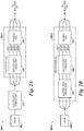
- Figure 2A illustrates a portion of a preparation cell of an apparatus 200-1 for single ion addressing in accordance with one or embodiments of the present disclosure
- Figure 2B illustrates a portion of a preparation cell of an apparatus 200-2 for single ion addressing in accordance with one or embodiments of the present disclosure
- Apparatus 200-1 and/or apparatus 200-2 can be, for example, apparatus 100 previously described in connection with Figure 1 .
- apparatus 200-1 can include preparation cell 202-1
- apparatus 200-2 can include preparation cell 202-2.
- Preparation cell 202-1 and/or preparation cell 202-2 can be, for example, preparation cell 102 previously described in connection with Figure 1 .
- apparatus 200-1 includes a laser (e.g., incident laser) 220-1
- apparatus 200-2 includes a laser (e.g., incident laser) 220-2.
- Laser 220-1 can be a Doppler cooling laser (e.g., a laser used in a Doppler cooling mechanism)
- laser 220-2 can be a quantum operation laser (e.g., a laser used in a quantum operation, such as Raman cooling, state preparation, photoionization, loading, and/or ion transitions, for instance).
- the embodiment illustrated in Figure 2A can include a Doppler cooling laser
- the embodiment illustrated in Figure 2B can include a quantum operation laser.
- the laser may be a 369 nanometer (nm) laser.
- embodiments of the present disclosure are not limited to a particular type of laser.
- apparatuses 200-1 and 200-2 can each include an electro-optic modulator 222.
- electro-optic modulator 220 is separate from (e.g., located outside of) preparation cell 202-1, and in the embodiment illustrated in Figure 2B , electro-optic modulator 220 is included in (e.g., located within) preparation cell 202-2.
- electro-optic modulator 222 may be a 7.37 GHz electro-optic modulator, and in the embodiment illustrated in Figure 2B , electro-optic modulator 222 may be a 2.1 GHz electro-optic modulator.
- embodiments of the present disclosure are not limited to a particular type of electro-optic modulator.
- electro-optic modulator 222 can prepare the state of laser 220-1 (e.g., the state of a laser beam emitted by laser 220-1), and in the embodiment illustrated in Figure 2B , electro-optic modulator 222 can prepare the state of laser 220-2 (e.g., the state of a laser beam emitted by laser 220-2). For example, electro-optic modulator 222 can generate large spacing sidebands for the state preparation, and address hyperfine transitions.
- electro-optic modulator 222 can prepare the state of laser 220-1 before the laser enters preparation cell 202-1. That is, in the embodiment illustrated in Figure 2A , the state of the laser may already be prepared when the laser enters preparation cell 202-1.
- the laser may split into a plurality of components (e.g., fibers) 212-1, 212-2, 212-3, 212-4 that separately enter preparation cell 202-1, as illustrated in Figure 2A . That is, in the embodiment illustrated in Figure 2A , electro-optic modulator 222 may be placed before preparation cell 202-1 and before the fiber split occurs.
- components e.g., fibers
- electro-optic modulator 222 in such a manner can reduce the complexity of apparatus 200-1, as it may mean apparatus 200-1 may need only one electro-optic modulator (e.g., instead of needing a separate electro-optic modulator for each Doppler cooling beam).
- Components 212-1, 212-2, 212-3, and 212-4 can be, for example, fibers 112-1, 112-2, 112-3, 112-2 previously described in connection with Figure 1 .
- Laser 220-1 may be split into components (e.g., fibers) 212-1, 212-2, 212-3, 212-4 by, for example, a fiber bundle (not shown in Figure 2A ), such as, for instance, fiber bundle 110 previously described in connection with Figure 1 .
- a fiber bundle not shown in Figure 2A
- fiber bundle 110 previously described in connection with Figure 1 .
- the embodiment illustrated in Figure 2A includes four fibers, embodiments of the present disclosure are not limited to a particular number of fibers.
- electro-optic modulator 222 can prepare the state of laser 220-2 after the laser enters preparation cell 202-2. That is, in the embodiment illustrated in Figure 2B , preparation cell 202-2 may prepare the state of the laser.
- the laser may split into a plurality of components (e.g., fibers) 212-1, 212-2, 212-3, 212-4 before the laser enters preparation cell 202-2 and before electro-optic modulator 222 prepares the state of the laser, such that each component separately enters preparation cell 202-1 and electro-optic modulator 222, as illustrated in Figure 2B . That is, in the embodiment illustrated in Figure 2B , electro-optic modulator 222 may be placed within preparation cell 202-2 and after the fiber split occurs.
- components e.g., fibers
- preparation cell 202-2 may include a separate electro-optic modulator for each component 212-1, 212-2, 212-3, 212-4 (e.g., component 212-1 may enter a first electro-optic modulator in preparation cell 202-2, component 212-2 may enter a second electro-optic modulator in preparation cell 202-2, etc.).
- each electro-optic modulator may have individual control, and prepare the state, of each beam component, allowing for state preparation of individual quantum and giving each beam component the ability to set and interrogate ytterbium's hyperfine quantum states.
- Components 212-1, 212-2, 212-3, and 212-4 can be, for example, fibers 112-1, 112-2, 112-3, 112-2 previously described in connection with Figure 1 .
- Laser 220-2 may be split into components (e.g., fibers) 212-1, 212-2, 212-3, 212-4 by, for example, a fiber bundle (not shown in Figure 2B ), such as, for instance, fiber bundle 110 previously described in connection with Figure 1 .
- a fiber bundle not shown in Figure 2B
- fiber bundle 110 previously described in connection with Figure 1 .
- the embodiment illustrated in Figure 2B includes four fibers, embodiments of the present disclosure are not limited to a particular number of fibers.
- preparation cells 202-1 and 202-2 can each include an acousto-optic modulator 224.
- preparation cells 202-1 and 202-2 can include an individual (e.g., separate) acousto-optic modulator for each laser component 212-1, 212-2, 212-3, 212-4, in a manner analogous to the separate electro-optic modulators of preparation cell 202-2.
- acousto-optic modulator 224 can be 200 MHz acousto-optic modulator.
- embodiments of the present disclosure are not limited to a particular type of acousto-optic modulator.
- acousto-optic modulator 224 can set the frequency and intensity of laser 220-1 and shutter laser 220-1 (e.g., each separate acousto-optic modulator can set the frequency and intensity of and shutter its respective laser component 212-1, 212-2, 212-3, 212-4) after electro-optic modulator 222 prepares the state of laser 220.
- acousto-optic modulator 224 can set the frequency and intensity of laser 220-2 and shutter laser 220-2 (e.g., each separate acousto-optic modulator can set the frequency and intensity of and shutter its respective laser component 212-1, 212-2, 212-3, 212-4) after electro-optic modulator 222 prepares the state of laser 220 (e.g., after each separate electro-optic modulator prepares the state of its respective laser component 212-1, 212-2, 212-3, 212-4).
- Light leakage from acousto-optic modulator 224 e,g, from the shutter of the acousto-optic modulator
- RF radio-frequency
- preparation cells 202-1 and 202-2 can each include a Pockels cell 226 (e.g., a voltage-controlled wave plate).
- preparation cells 202-1 and 202-2 can include an individual (e.g., separate) Pockels cell for each laser component 212-1, 212-2, 212-3, 212-4, in a manner analogous to the separate electro-optic modulators of preparation cell 202-2.
- Pockels cell 226 can set the polarization of laser 220-1 (e.g., each separate Pockels cell can set the polarization of its respective laser component 212-1, 212-2, 212-3, 212-4) after acousto-optic modulator 224 sets the frequency and intensity of laser 220-1 and shutters laser 220-1.
- Pockels cell 226 can set the polarization of laser 220-2 (e.g., each respective Pockels cell can set the polarization of its respective laser component 212-1, 212-2, 212-3, 212-4) after acousto-optic modulator 224 sets the frequency and intensity of laser 220-2 and shutters laser 220-2.
- Pockels cell 226 can be used to prevent electro-optic modulator 222 and/or acousto-optic modulator 224 from disturbing the polarization state of the laser since it is placed after these two devices.
- laser components 212-1, 212-2, 212-3, 212-4 may bundle (e.g., re-bundle) after exiting preparation cells 202-1 and 202-2, respectively.
- the bundled components e.g., fibers
- the bundled components may then enter a vacuum (e.g., vacuum 108 previously described in connection with Figure 1 ) and travel to an alignment cell (e.g., alignment cell 104 previously described in connection with Figure 1 ).
- Laser components 212-1, 212-2, 212-3, 212-4 may be bundled by, for example, an additional fiber bundle (not shown in Figures 2A and 2B ), such as, for instance, fiber bundle 114 previously described in connection with Figure 1 .
- FIG 3 illustrates a portion of an alignment cell 304 of an apparatus for single ion addressing in accordance with one or embodiments of the present disclosure.
- Alignment cell 304 can be, for example, alignment cell 104 of apparatus 100 previously described in connection with Figure 1 .
- a first component 320-1 and a second component 320-2 of a laser (e.g., laser beam) from a preparation cell can enter alignment cell 304.
- laser component 320-1 can enter (e.g. be input into) alignment cell 304 from a first fiber (e.g., fiber 112-1 previously described in connection with Figure 1 ), and laser component 320-2 can enter alignment cell from a second fiber (e.g., fiber 112-2 previously described in connection with Figure 1 ), as previously described herein (e.g., in connection with Figure 1 ).
- Laser component 320-1 can be a component of laser 220-1 previously described in connection with Figure 2A
- laser component 320-2 can be a component of laser 220-2 previously described in connection with Figure 2B . That is, in the embodiment illustrated in Figure 3 , laser component 320-1 can be a component of a Doppler cooling laser, and laser component 320-2 can be a component of a quantum operation laser.
- embodiments of the present disclosure are not limited to a particular type of laser.
- alignment cell 304 can include a first lens 332-1 and a second lens 332-2.
- Lenses 332-1 and 332-2 can be, for example, ball lenses. Further, the focal length of lenses 332-1 and 332-2 can be set to garner a particular beam waist and location for a given ion operation.
- lens 332-1 can focus laser component 320-1, and direct laser component 320-1 at mirror 334-1 formed (e.g., placed) on the surface of chip (e.g., die) 346.
- Lens 332-2 can focus laser component 320-2, and direct laser component 320-2 at mirror 334-1 formed on the surface of chip 346.
- the distance between the centers of lenses 332-1 and 332-2 and the surface of chip 346 can be, for example, three millimeters (mm).
- mirror 334-1 can direct (e.g., reflect) the focused laser component 320-1 at ion 336-1 trapped in an ion trap formed on chip 346, such that ion 336-1 is illuminated by focused laser component 320-1.
- Mirror 334-2 can direct the focused laser component 320-2 at ion 336-2 that may be trapped in an additional ion trap formed on chip 346, such that ion 336-2 is illuminated by focused laser component 320-2.
- the distance between mirror 334-1 and ion 336-1, and the distance between mirror 334-2 and ion 336-2, can be, for example, 2.5 mm.
- the distance between ion 336-1 and 336-2 can be, for example, 0.5 mm.
- Ions 336-1 and 336-2 can be, for example, Yb ions. However, embodiments of the present disclosure are not limited to a particular type of ion.
- ion 336-2 may fluoresce (e.g., emit) light 338 and/or perform a quantum operation when illuminated by focused laser component 320-2.
- Fluoresced light 338 can be received (e.g., coupled) by lens 340 of alignment cell 304, as illustrated in Figure 3 .
- Lens 340 can be, for example, a ball lens having a diameter of 2 mm. Further, the focal length of lens 340 can be set to couple fluoresced light 338 into a fiber (e.g., output fiber) exiting alignment cell 304.
- fluoresced light 338 can exit alignment cell 304 after being received (e.g., coupled) by lens 340, and travel to a detection cell (e.g., detection cell 106 previously described in connection with Figure 1 ).
- a detection cell e.g., detection cell 106 previously described in connection with Figure 1
- fluoresced light 338 can exit (e.g. be output from) alignment cell 304, and travel to the detection cell, through a fiber (e.g., fiber 116-1 or 116-2 previously described in connection with Figure 1 ), as previously described herein (e.g., in connection with Figure 1 ).
- mirror 342-1 formed on the surface of chip 346 can direct (e.g., reflect) laser component 320-1 at beam dump 344 of alignment cell 304 after laser component 320-1 is aligned to (e.g., focused at), and illuminates, ion 336-1.
- Mirror 342-2 formed on the surface of chip 346 can direct laser component 320-2 at beam dump 344 after laser component 320-2 is aligned to, and illuminates, ion 336-2.
- Laser components 320-1 and 320-2 can terminate at (e.g., upon reaching) beam dump 344. Terminating laser components 320-1 and 320-2 at beam dump 344 can mitigate stray light and/or heating in alignment cell 304.
- Alignment cell 304 may be designed as a unit cell that can be repeated across an array (e.g., a 2D array) of ion traps formed on chip 346. That is, the embodiment illustrated in Figure 3 can be repeated across an array of ion traps formed on chip 346. However, only one alignment cell 304 has been shown in Figure 3 for clarity and so as not to obscure embodiments of the present disclosure.
Landscapes
- Health & Medical Sciences (AREA)
- Physics & Mathematics (AREA)
- Chemical & Material Sciences (AREA)
- Analytical Chemistry (AREA)
- General Physics & Mathematics (AREA)
- Biochemistry (AREA)
- General Health & Medical Sciences (AREA)
- Nuclear Medicine, Radiotherapy & Molecular Imaging (AREA)
- Immunology (AREA)
- Pathology (AREA)
- Life Sciences & Earth Sciences (AREA)
- Engineering & Computer Science (AREA)
- Optics & Photonics (AREA)
- Mechanical Engineering (AREA)
- Thermal Sciences (AREA)
- General Engineering & Computer Science (AREA)
- Optical Modulation, Optical Deflection, Nonlinear Optics, Optical Demodulation, Optical Logic Elements (AREA)
- Lasers (AREA)
- Investigating, Analyzing Materials By Fluorescence Or Luminescence (AREA)
Claims (10)
- Vorrichtung (100, 200-1, 200-2) für Einzelionenadressierung, umfassend:eine erste optische Zelle (102, 202-1, 202-2), die ausgelegt ist zum:Einstellen einer Frequenz, einer Intensität und einer Polarisation eines Laserstrahls, der von einem Einzellaser (220-1, 220-2) abgestrahlt wird; undAbblenden des Laserstrahls, der von dem Einzellaser (220-1, 220-2) abgestrahlt wird;eine zweite optische Zelle (104, 304), die dafür ausgelegt ist, den abgeblendeten Laserstrahl (320-2), der von dem Einzellaser (220-1, 220-2) abgestrahlt wird, auf ein Ion (336-2) in einer Ionenfalle, die auf der Oberfläche eines Chips (346) ausgebildet ist, auszurichten, derart, dass das Ion (336-2) Licht (338) fluoresziert, und/oder eine Quantenoperation durchführt, wenn das Ion (336-2) durch den abgeblendeten Laserstrahl (320-2), der von dem Einzellaser (220-1, 220-2) abgestrahlt wird, beleuchtet wird, wobei die zweite optische Zelle (104, 304) aufweist:einen Chip, der die Oberfläche aufweist, auf der die Ionenfalle ausgebildet ist;eine Linse (332-2), die dafür ausgelegt ist, den abgeblendeten Laserstrahl (320-2), der von dem Einzellaser (220-1, 220-2) abgestrahlt wird, zu fokussieren; undeinen Spiegel (334-2), der auf der Oberfläche des Chips (346) ausgebildet ist, auf dem die Ionenfalle ausgebildet ist, wobei der Spiegel (334-2) dafür ausgelegt ist, den fokussierten, abgeblendeten Laserstrahl (320-2), der von dem Einzellaser (220-1, 220-2) abgestrahlt wird, auf ein Ion (336-2) in der Ionenfalle zu richten, derart, dass das Ion (336-2) durch den fokussierten, abgeblendeten Laserstrahl (320-2) beleuchtet wird; undeine dritte optische Zelle (106), die dafür ausgelegt ist, das Licht (338) zu detektieren, das von dem Ion (336-2) fluoresziert wird, wenn das Ion (336-2) durch den abgeblendeten Laserstrahl (320-2), der von dem Einzellaser (220-1, 220-2) abgestrahlt wird, beleuchtet wird.
- Vorrichtung (100, 200-1, 200-2) nach Anspruch 1, wobei:die zweite optische Zelle (104, 304) in einem Vakuum liegt (108); unddie erste und die dritte optische Zelle (102, 202-1, 202-2, 106) außerhalb des Vakuums (108) liegen.
- Vorrichtung (100, 200-1) nach Anspruch 1, wobei die Vorrichtung (100, 200-1) einen elektrooptischen Modulator (222) aufweist, der von der ersten optischen Zelle (102, 202-1) getrennt und dafür ausgelegt ist, einen Zustand des Laserstrahls, der von dem Einzellaser (220-1) abgestrahlt wird, vorzubereiten, bevor der Laserstrahl in die erste optische Zelle (102, 202-1) eintritt.
- Vorrichtung (100, 200-1, 200-2) nach Anspruch 1, wobei die erste optische Zelle (102, 202-2) einen elektrooptischen Modulator (222) aufweist, der dafür ausgelegt ist, einen Zustand des Laserstrahls, der von dem Einzellaser (220-2) abgestrahlt wird, vorzubereiten.
- Vorrichtung (100, 200-1, 200-2) nach Anspruch 1, wobei die erste optische Zelle (102, 202-1, 202-2) aufweist:einen akustooptischen Modulator (224), der dafür ausgelegt ist, die Frequenz und die Intensität des Laserstrahls, der von dem Einzellaser (220-1, 220-2) abgestrahlt wird, einzustellen und den Laserstrahl, der von dem Einzellaser (220-1, 220-2) abgestrahlt wird, abzublenden; undeine Pockels-Zelle (226), die dafür ausgelegt ist, die Polarisation des Laserstrahls, der von dem Einzellaser (220-1, 220-2) abgestrahlt wird, einzustellen.
- Vorrichtung (100, 200-1, 200-2) nach Anspruch 1, wobei die dritte optische Zelle (106) eine Anordnung von Photovervielfacherröhren aufweist, die dafür ausgelegt ist, das Licht (338) zu detektieren, das von dem Ion (336-2) fluoresziert wird, wenn das Ion (336-2) durch den abgeblendeten Laserstrahl (320-2), der von dem Einzellaser (220-1, 220-2) abgestrahlt wird, beleuchtet wird.
- Vorrichtung (100, 200-1, 200-2) nach Anspruch 1, wobei die erste, die zweite und die dritte optische Zelle (102, 202-1, 202-2, 104, 304, 106) getrennte optische Zellen sind.
- Vorrichtung (100, 200-1, 200-2) nach Anspruch 1, wobei:die zweite optische Zelle (104, 304) dafür ausgelegt ist, das Licht (338) zu empfangen, das von dem Ion (336-2) fluoresziert wird, wenn das Ion (336-2) durch den abgeblendeten Laserstrahl (320-2), der von dem Einzellaser (220-1, 220-2) abgestrahlt wird, beleuchtet wird; unddie dritte optische Zelle (106) dafür ausgelegt ist, das Licht (338) zu empfangen, das von dem Ion (336-2) aus der zweiten optischen Zelle (104, 304) fluoresziert wird.
- Vorrichtung (100, 200-1, 200-2) nach Anspruch 1, wobei der Einzellaser (220-2) ein Quantenbetriebslaser ist.
- Vorrichtung (100, 200-1, 200-2) nach Anspruch 1, wobei der Einzellaser (220-1) ein Doppler-Kühllaser ist.
Applications Claiming Priority (1)
| Application Number | Priority Date | Filing Date | Title |
|---|---|---|---|
| US14/686,553 US9588047B2 (en) | 2015-04-14 | 2015-04-14 | Multi-cell apparatus and method for single ion addressing |
Publications (2)
| Publication Number | Publication Date |
|---|---|
| EP3088869A1 EP3088869A1 (de) | 2016-11-02 |
| EP3088869B1 true EP3088869B1 (de) | 2018-09-05 |
Family
ID=55345717
Family Applications (1)
| Application Number | Title | Priority Date | Filing Date |
|---|---|---|---|
| EP16154696.5A Active EP3088869B1 (de) | 2015-04-14 | 2016-02-08 | Mehrzellige vorrichtung und verfahren für einzelionenadressierung |
Country Status (2)
| Country | Link |
|---|---|
| US (2) | US9588047B2 (de) |
| EP (1) | EP3088869B1 (de) |
Families Citing this family (7)
| Publication number | Priority date | Publication date | Assignee | Title |
|---|---|---|---|---|
| CN106050834A (zh) * | 2016-08-12 | 2016-10-26 | 中山大山摄影器材有限公司 | 快速连接结构 |
| GB201802917D0 (en) | 2018-02-22 | 2018-04-11 | Micromass Ltd | Charge detection mass spectrometry |
| SG10201801853WA (en) * | 2018-03-02 | 2019-10-30 | Delta Electronics Int’L Singapore Pte Ltd | Portable multi-color fluorescence detection device |
| US11842891B2 (en) | 2020-04-09 | 2023-12-12 | Waters Technologies Corporation | Ion detector |
| WO2023111707A1 (en) | 2021-12-15 | 2023-06-22 | Waters Technologies Corporation | An inductive detector with integrated amplifier |
| US11809839B2 (en) | 2022-01-18 | 2023-11-07 | Robert Lyden | Computer language and code for application development and electronic and optical communication |
| GB2625747A (en) * | 2022-12-22 | 2024-07-03 | Universal Quantum Ltd | Improvements in or relating to quantum computing |
Family Cites Families (17)
| Publication number | Priority date | Publication date | Assignee | Title |
|---|---|---|---|---|
| US6753253B1 (en) * | 1986-06-18 | 2004-06-22 | Hitachi, Ltd. | Method of making wiring and logic corrections on a semiconductor device by use of focused ion beams |
| US5527731A (en) * | 1992-11-13 | 1996-06-18 | Hitachi, Ltd. | Surface treating method and apparatus therefor |
| JP3509267B2 (ja) * | 1995-04-03 | 2004-03-22 | 株式会社日立製作所 | イオントラップ質量分析方法および装置 |
| US6489609B1 (en) * | 1999-05-21 | 2002-12-03 | Hitachi, Ltd. | Ion trap mass spectrometry and apparatus |
| WO2000077821A1 (en) * | 1999-06-14 | 2000-12-21 | Isis Pharmaceuticals, Inc. | External shutter for electrospray ionization mass spectrometry |
| AU2001275364A1 (en) * | 2000-06-09 | 2001-12-24 | University Of Delaware | System and method for chemical analysis using laser ablation |
| US6777671B2 (en) * | 2001-04-10 | 2004-08-17 | Science & Engineering Services, Inc. | Time-of-flight/ion trap mass spectrometer, a method, and a computer program product to use the same |
| US8073627B2 (en) * | 2001-06-26 | 2011-12-06 | Ibis Biosciences, Inc. | System for indentification of pathogens |
| GB2414855A (en) * | 2004-03-30 | 2005-12-07 | Thermo Finnigan Llc | Ion fragmentation by electron capture |
| DE102004061820A1 (de) * | 2004-12-22 | 2006-07-06 | Bruker Daltonik Gmbh | Lasersystem für die lonisation durch matrixunterstützte Laserdesorption (MALDI) im ultravioletten Spektralbereich (UV) |
| US7518120B2 (en) | 2005-01-04 | 2009-04-14 | The Regents Of The University Of Michigan | Long-distance quantum communication and scalable quantum computation |
| US7180078B2 (en) | 2005-02-01 | 2007-02-20 | Lucent Technologies Inc. | Integrated planar ion traps |
| US7709807B2 (en) * | 2007-05-31 | 2010-05-04 | United States Of America As Represented By The Secretary Of Commerce, The National Institute Of Standards And Technology | Magneto-optical trap ion source |
| US7859350B1 (en) | 2009-04-28 | 2010-12-28 | Sandia Corporation | Microfabricated ion frequency standard |
| US20100316176A1 (en) * | 2009-06-12 | 2010-12-16 | Wood Mark A | System and method for remotely-inducible variable-element electro-chemical-nuclear disruption |
| GB201208843D0 (en) * | 2012-05-18 | 2012-07-04 | Fasmatech Science And Technology Llc | Improvements in and relating to mass or size measurement of ions |
| US10096458B2 (en) * | 2013-05-31 | 2018-10-09 | Micromass Uk Limited | Compact mass spectrometer |
-
2015
- 2015-04-14 US US14/686,553 patent/US9588047B2/en active Active
-
2016
- 2016-02-08 EP EP16154696.5A patent/EP3088869B1/de active Active
-
2017
- 2017-01-23 US US15/412,857 patent/US10145792B2/en active Active
Also Published As
| Publication number | Publication date |
|---|---|
| EP3088869A1 (de) | 2016-11-02 |
| US9588047B2 (en) | 2017-03-07 |
| US20170122868A1 (en) | 2017-05-04 |
| US20160305879A1 (en) | 2016-10-20 |
| US10145792B2 (en) | 2018-12-04 |
Similar Documents
| Publication | Publication Date | Title |
|---|---|---|
| EP3088869A1 (de) | Mehrzellige vorrichtung und verfahren für einzelionenadressierung | |
| US10340052B2 (en) | Single cell apparatus and method for single ion addressing | |
| JP7432600B2 (ja) | 効率的な広視野蛍光寿命顕微鏡法を可能にする電気光学イメージング | |
| Hannig et al. | Towards a transportable aluminium ion quantum logic optical clock | |
| CN101821607B (zh) | 用于使样本中的用荧光染料标记的结构成像的方法和装置 | |
| Tsai et al. | In vivo two-photon laser scanning microscopy with concurrent plasma-mediated ablation principles and hardware realization | |
| EP2522969A2 (de) | Nichtlineare ramanspektroskopische Vorrichtung mit einer Monomode-Faser zur Erzeugung des Stokes-Strahls | |
| EP3538948B1 (de) | Räumlich-zeitlich inkrementelle gewobbelte faserquelle | |
| US9810966B2 (en) | Random access stimulated emission depletion (STED) microscopy | |
| Görlitz et al. | easySLM‐STED: stimulated emission depletion microscopy with aberration correction, extended field of view and multiple beam scanning | |
| Trokhimchuck | Relaxed Optics: Modelling and Discussions 3 | |
| CN208924248U (zh) | 多通道相干拉曼散射光学系统和成像系统 | |
| CN102902056B (zh) | 基于量子统计的高精度光学成像装置与方法 | |
| JP6058658B2 (ja) | レーザー−電子間の拡張相互作用を介する高フラックス且つ狭帯域のコンプトン光源 | |
| CN103162845A (zh) | 飞秒时域单光子空间多波长探测装置 | |
| US10803996B2 (en) | Plasma diagnosis system using multiple-reciprocating-pass Thompson scattering | |
| CN116148232B (zh) | 一种全谱荧光寿命快速测量装置 | |
| CN108964781A (zh) | 多通道相干拉曼散射光学装置和成像系统 | |
| Fernandez-Gonzalvo et al. | A fully fiber-integrated ion trap for portable quantum technologies | |
| US10866189B2 (en) | Optical measurement apparatus and optical measurement method | |
| WO2021174211A1 (en) | Two-photon fluorescence microscopy at extremely low excitation intensity | |
| EP3081924A1 (de) | Optische aufbereitungszelle und verfahren | |
| WO2020152059A1 (en) | Pulse shaping for stimulated emission depletion microscopy | |
| Fernandez-Gonzalvo et al. | A Fully Fiber-Integrated Ion Trap for Portable Optical Atomic Clocks | |
| He et al. | Wavelength separation tunable 2-color soliton generation and its application to 2-color fluorescence multiphoton microscopy |
Legal Events
| Date | Code | Title | Description |
|---|---|---|---|
| PUAI | Public reference made under article 153(3) epc to a published international application that has entered the european phase |
Free format text: ORIGINAL CODE: 0009012 |
|
| 17P | Request for examination filed |
Effective date: 20160208 |
|
| AK | Designated contracting states |
Kind code of ref document: A1 Designated state(s): AL AT BE BG CH CY CZ DE DK EE ES FI FR GB GR HR HU IE IS IT LI LT LU LV MC MK MT NL NO PL PT RO RS SE SI SK SM TR |
|
| AX | Request for extension of the european patent |
Extension state: BA ME |
|
| STAA | Information on the status of an ep patent application or granted ep patent |
Free format text: STATUS: EXAMINATION IS IN PROGRESS |
|
| 17Q | First examination report despatched |
Effective date: 20170626 |
|
| GRAP | Despatch of communication of intention to grant a patent |
Free format text: ORIGINAL CODE: EPIDOSNIGR1 |
|
| STAA | Information on the status of an ep patent application or granted ep patent |
Free format text: STATUS: GRANT OF PATENT IS INTENDED |
|
| INTG | Intention to grant announced |
Effective date: 20180412 |
|
| GRAS | Grant fee paid |
Free format text: ORIGINAL CODE: EPIDOSNIGR3 |
|
| GRAA | (expected) grant |
Free format text: ORIGINAL CODE: 0009210 |
|
| STAA | Information on the status of an ep patent application or granted ep patent |
Free format text: STATUS: THE PATENT HAS BEEN GRANTED |
|
| AK | Designated contracting states |
Kind code of ref document: B1 Designated state(s): AL AT BE BG CH CY CZ DE DK EE ES FI FR GB GR HR HU IE IS IT LI LT LU LV MC MK MT NL NO PL PT RO RS SE SI SK SM TR |
|
| REG | Reference to a national code |
Ref country code: GB Ref legal event code: FG4D |
|
| REG | Reference to a national code |
Ref country code: CH Ref legal event code: EP |
|
| REG | Reference to a national code |
Ref country code: AT Ref legal event code: REF Ref document number: 1038403 Country of ref document: AT Kind code of ref document: T Effective date: 20180915 |
|
| REG | Reference to a national code |
Ref country code: IE Ref legal event code: FG4D |
|
| REG | Reference to a national code |
Ref country code: DE Ref legal event code: R096 Ref document number: 602016005236 Country of ref document: DE |
|
| REG | Reference to a national code |
Ref country code: NL Ref legal event code: MP Effective date: 20180905 |
|
| REG | Reference to a national code |
Ref country code: LT Ref legal event code: MG4D |
|
| PG25 | Lapsed in a contracting state [announced via postgrant information from national office to epo] |
Ref country code: FI Free format text: LAPSE BECAUSE OF FAILURE TO SUBMIT A TRANSLATION OF THE DESCRIPTION OR TO PAY THE FEE WITHIN THE PRESCRIBED TIME-LIMIT Effective date: 20180905 Ref country code: LT Free format text: LAPSE BECAUSE OF FAILURE TO SUBMIT A TRANSLATION OF THE DESCRIPTION OR TO PAY THE FEE WITHIN THE PRESCRIBED TIME-LIMIT Effective date: 20180905 Ref country code: BG Free format text: LAPSE BECAUSE OF FAILURE TO SUBMIT A TRANSLATION OF THE DESCRIPTION OR TO PAY THE FEE WITHIN THE PRESCRIBED TIME-LIMIT Effective date: 20181205 Ref country code: GR Free format text: LAPSE BECAUSE OF FAILURE TO SUBMIT A TRANSLATION OF THE DESCRIPTION OR TO PAY THE FEE WITHIN THE PRESCRIBED TIME-LIMIT Effective date: 20181206 Ref country code: NO Free format text: LAPSE BECAUSE OF FAILURE TO SUBMIT A TRANSLATION OF THE DESCRIPTION OR TO PAY THE FEE WITHIN THE PRESCRIBED TIME-LIMIT Effective date: 20181205 Ref country code: RS Free format text: LAPSE BECAUSE OF FAILURE TO SUBMIT A TRANSLATION OF THE DESCRIPTION OR TO PAY THE FEE WITHIN THE PRESCRIBED TIME-LIMIT Effective date: 20180905 Ref country code: SE Free format text: LAPSE BECAUSE OF FAILURE TO SUBMIT A TRANSLATION OF THE DESCRIPTION OR TO PAY THE FEE WITHIN THE PRESCRIBED TIME-LIMIT Effective date: 20180905 |
|
| REG | Reference to a national code |
Ref country code: AT Ref legal event code: MK05 Ref document number: 1038403 Country of ref document: AT Kind code of ref document: T Effective date: 20180905 |
|
| PG25 | Lapsed in a contracting state [announced via postgrant information from national office to epo] |
Ref country code: AL Free format text: LAPSE BECAUSE OF FAILURE TO SUBMIT A TRANSLATION OF THE DESCRIPTION OR TO PAY THE FEE WITHIN THE PRESCRIBED TIME-LIMIT Effective date: 20180905 Ref country code: LV Free format text: LAPSE BECAUSE OF FAILURE TO SUBMIT A TRANSLATION OF THE DESCRIPTION OR TO PAY THE FEE WITHIN THE PRESCRIBED TIME-LIMIT Effective date: 20180905 Ref country code: HR Free format text: LAPSE BECAUSE OF FAILURE TO SUBMIT A TRANSLATION OF THE DESCRIPTION OR TO PAY THE FEE WITHIN THE PRESCRIBED TIME-LIMIT Effective date: 20180905 |
|
| PG25 | Lapsed in a contracting state [announced via postgrant information from national office to epo] |
Ref country code: IT Free format text: LAPSE BECAUSE OF FAILURE TO SUBMIT A TRANSLATION OF THE DESCRIPTION OR TO PAY THE FEE WITHIN THE PRESCRIBED TIME-LIMIT Effective date: 20180905 Ref country code: PL Free format text: LAPSE BECAUSE OF FAILURE TO SUBMIT A TRANSLATION OF THE DESCRIPTION OR TO PAY THE FEE WITHIN THE PRESCRIBED TIME-LIMIT Effective date: 20180905 Ref country code: AT Free format text: LAPSE BECAUSE OF FAILURE TO SUBMIT A TRANSLATION OF THE DESCRIPTION OR TO PAY THE FEE WITHIN THE PRESCRIBED TIME-LIMIT Effective date: 20180905 Ref country code: EE Free format text: LAPSE BECAUSE OF FAILURE TO SUBMIT A TRANSLATION OF THE DESCRIPTION OR TO PAY THE FEE WITHIN THE PRESCRIBED TIME-LIMIT Effective date: 20180905 Ref country code: RO Free format text: LAPSE BECAUSE OF FAILURE TO SUBMIT A TRANSLATION OF THE DESCRIPTION OR TO PAY THE FEE WITHIN THE PRESCRIBED TIME-LIMIT Effective date: 20180905 Ref country code: IS Free format text: LAPSE BECAUSE OF FAILURE TO SUBMIT A TRANSLATION OF THE DESCRIPTION OR TO PAY THE FEE WITHIN THE PRESCRIBED TIME-LIMIT Effective date: 20190105 Ref country code: ES Free format text: LAPSE BECAUSE OF FAILURE TO SUBMIT A TRANSLATION OF THE DESCRIPTION OR TO PAY THE FEE WITHIN THE PRESCRIBED TIME-LIMIT Effective date: 20180905 Ref country code: CZ Free format text: LAPSE BECAUSE OF FAILURE TO SUBMIT A TRANSLATION OF THE DESCRIPTION OR TO PAY THE FEE WITHIN THE PRESCRIBED TIME-LIMIT Effective date: 20180905 Ref country code: NL Free format text: LAPSE BECAUSE OF FAILURE TO SUBMIT A TRANSLATION OF THE DESCRIPTION OR TO PAY THE FEE WITHIN THE PRESCRIBED TIME-LIMIT Effective date: 20180905 |
|
| PG25 | Lapsed in a contracting state [announced via postgrant information from national office to epo] |
Ref country code: SK Free format text: LAPSE BECAUSE OF FAILURE TO SUBMIT A TRANSLATION OF THE DESCRIPTION OR TO PAY THE FEE WITHIN THE PRESCRIBED TIME-LIMIT Effective date: 20180905 Ref country code: PT Free format text: LAPSE BECAUSE OF FAILURE TO SUBMIT A TRANSLATION OF THE DESCRIPTION OR TO PAY THE FEE WITHIN THE PRESCRIBED TIME-LIMIT Effective date: 20190105 Ref country code: SM Free format text: LAPSE BECAUSE OF FAILURE TO SUBMIT A TRANSLATION OF THE DESCRIPTION OR TO PAY THE FEE WITHIN THE PRESCRIBED TIME-LIMIT Effective date: 20180905 |
|
| REG | Reference to a national code |
Ref country code: DE Ref legal event code: R097 Ref document number: 602016005236 Country of ref document: DE |
|
| PLBE | No opposition filed within time limit |
Free format text: ORIGINAL CODE: 0009261 |
|
| STAA | Information on the status of an ep patent application or granted ep patent |
Free format text: STATUS: NO OPPOSITION FILED WITHIN TIME LIMIT |
|
| PG25 | Lapsed in a contracting state [announced via postgrant information from national office to epo] |
Ref country code: DK Free format text: LAPSE BECAUSE OF FAILURE TO SUBMIT A TRANSLATION OF THE DESCRIPTION OR TO PAY THE FEE WITHIN THE PRESCRIBED TIME-LIMIT Effective date: 20180905 |
|
| 26N | No opposition filed |
Effective date: 20190606 |
|
| PG25 | Lapsed in a contracting state [announced via postgrant information from national office to epo] |
Ref country code: SI Free format text: LAPSE BECAUSE OF FAILURE TO SUBMIT A TRANSLATION OF THE DESCRIPTION OR TO PAY THE FEE WITHIN THE PRESCRIBED TIME-LIMIT Effective date: 20180905 |
|
| REG | Reference to a national code |
Ref country code: CH Ref legal event code: PL |
|
| PG25 | Lapsed in a contracting state [announced via postgrant information from national office to epo] |
Ref country code: LU Free format text: LAPSE BECAUSE OF NON-PAYMENT OF DUE FEES Effective date: 20190208 Ref country code: MC Free format text: LAPSE BECAUSE OF FAILURE TO SUBMIT A TRANSLATION OF THE DESCRIPTION OR TO PAY THE FEE WITHIN THE PRESCRIBED TIME-LIMIT Effective date: 20180905 |
|
| REG | Reference to a national code |
Ref country code: BE Ref legal event code: MM Effective date: 20190228 |
|
| REG | Reference to a national code |
Ref country code: IE Ref legal event code: MM4A |
|
| PG25 | Lapsed in a contracting state [announced via postgrant information from national office to epo] |
Ref country code: CH Free format text: LAPSE BECAUSE OF NON-PAYMENT OF DUE FEES Effective date: 20190228 Ref country code: LI Free format text: LAPSE BECAUSE OF NON-PAYMENT OF DUE FEES Effective date: 20190228 |
|
| PG25 | Lapsed in a contracting state [announced via postgrant information from national office to epo] |
Ref country code: IE Free format text: LAPSE BECAUSE OF NON-PAYMENT OF DUE FEES Effective date: 20190208 |
|
| PG25 | Lapsed in a contracting state [announced via postgrant information from national office to epo] |
Ref country code: FR Free format text: LAPSE BECAUSE OF NON-PAYMENT OF DUE FEES Effective date: 20190228 Ref country code: BE Free format text: LAPSE BECAUSE OF NON-PAYMENT OF DUE FEES Effective date: 20190228 |
|
| PG25 | Lapsed in a contracting state [announced via postgrant information from national office to epo] |
Ref country code: TR Free format text: LAPSE BECAUSE OF FAILURE TO SUBMIT A TRANSLATION OF THE DESCRIPTION OR TO PAY THE FEE WITHIN THE PRESCRIBED TIME-LIMIT Effective date: 20180905 |
|
| PG25 | Lapsed in a contracting state [announced via postgrant information from national office to epo] |
Ref country code: MT Free format text: LAPSE BECAUSE OF NON-PAYMENT OF DUE FEES Effective date: 20190208 |
|
| PG25 | Lapsed in a contracting state [announced via postgrant information from national office to epo] |
Ref country code: CY Free format text: LAPSE BECAUSE OF FAILURE TO SUBMIT A TRANSLATION OF THE DESCRIPTION OR TO PAY THE FEE WITHIN THE PRESCRIBED TIME-LIMIT Effective date: 20180905 |
|
| PG25 | Lapsed in a contracting state [announced via postgrant information from national office to epo] |
Ref country code: HU Free format text: LAPSE BECAUSE OF FAILURE TO SUBMIT A TRANSLATION OF THE DESCRIPTION OR TO PAY THE FEE WITHIN THE PRESCRIBED TIME-LIMIT; INVALID AB INITIO Effective date: 20160208 |
|
| PG25 | Lapsed in a contracting state [announced via postgrant information from national office to epo] |
Ref country code: MK Free format text: LAPSE BECAUSE OF FAILURE TO SUBMIT A TRANSLATION OF THE DESCRIPTION OR TO PAY THE FEE WITHIN THE PRESCRIBED TIME-LIMIT Effective date: 20180905 |
|
| P01 | Opt-out of the competence of the unified patent court (upc) registered |
Effective date: 20230526 |
|
| REG | Reference to a national code |
Ref country code: GB Ref legal event code: 732E Free format text: REGISTERED BETWEEN 20240125 AND 20240131 |
|
| REG | Reference to a national code |
Ref country code: DE Ref legal event code: R081 Ref document number: 602016005236 Country of ref document: DE Owner name: QUANTINUUM LLC, BROOMFIELD, US Free format text: FORMER OWNER: HONEYWELL INTERNATIONAL INC., MORRIS PLAINS, N.J., US |
|
| PGFP | Annual fee paid to national office [announced via postgrant information from national office to epo] |
Ref country code: GB Payment date: 20260227 Year of fee payment: 11 |
|
| PGFP | Annual fee paid to national office [announced via postgrant information from national office to epo] |
Ref country code: DE Payment date: 20260227 Year of fee payment: 11 |