EP3087595B1 - System and method for non-contact wafer chucking - Google Patents
System and method for non-contact wafer chucking Download PDFInfo
- Publication number
- EP3087595B1 EP3087595B1 EP14875288.4A EP14875288A EP3087595B1 EP 3087595 B1 EP3087595 B1 EP 3087595B1 EP 14875288 A EP14875288 A EP 14875288A EP 3087595 B1 EP3087595 B1 EP 3087595B1
- Authority
- EP
- European Patent Office
- Prior art keywords
- wafer
- wafer chuck
- elements
- chuck
- pressurized gas
- Prior art date
- Legal status (The legal status is an assumption and is not a legal conclusion. Google has not performed a legal analysis and makes no representation as to the accuracy of the status listed.)
- Active
Links
Images



Classifications
-
- H—ELECTRICITY
- H10—SEMICONDUCTOR DEVICES; ELECTRIC SOLID-STATE DEVICES NOT OTHERWISE PROVIDED FOR
- H10P—GENERIC PROCESSES OR APPARATUS FOR THE MANUFACTURE OR TREATMENT OF DEVICES COVERED BY CLASS H10
- H10P72/00—Handling or holding of wafers, substrates or devices during manufacture or treatment thereof
- H10P72/70—Handling or holding of wafers, substrates or devices during manufacture or treatment thereof for supporting or gripping
- H10P72/78—Handling or holding of wafers, substrates or devices during manufacture or treatment thereof for supporting or gripping using vacuum or suction, e.g. Bernoulli chucks
-
- G—PHYSICS
- G01—MEASURING; TESTING
- G01N—INVESTIGATING OR ANALYSING MATERIALS BY DETERMINING THEIR CHEMICAL OR PHYSICAL PROPERTIES
- G01N21/00—Investigating or analysing materials by the use of optical means, i.e. using sub-millimetre waves, infrared, visible or ultraviolet light
- G01N21/84—Systems specially adapted for particular applications
- G01N21/88—Investigating the presence of flaws or contamination
- G01N21/95—Investigating the presence of flaws or contamination characterised by the material or shape of the object to be examined
- G01N21/9501—Semiconductor wafers
- G01N21/9503—Wafer edge inspection
-
- H—ELECTRICITY
- H10—SEMICONDUCTOR DEVICES; ELECTRIC SOLID-STATE DEVICES NOT OTHERWISE PROVIDED FOR
- H10P—GENERIC PROCESSES OR APPARATUS FOR THE MANUFACTURE OR TREATMENT OF DEVICES COVERED BY CLASS H10
- H10P72/00—Handling or holding of wafers, substrates or devices during manufacture or treatment thereof
- H10P72/70—Handling or holding of wafers, substrates or devices during manufacture or treatment thereof for supporting or gripping
- H10P72/76—Handling or holding of wafers, substrates or devices during manufacture or treatment thereof for supporting or gripping using mechanical means, e.g. clamps or pinches
- H10P72/7604—Handling or holding of wafers, substrates or devices during manufacture or treatment thereof for supporting or gripping using mechanical means, e.g. clamps or pinches the wafers being placed on a susceptor, stage or support
- H10P72/7608—Handling or holding of wafers, substrates or devices during manufacture or treatment thereof for supporting or gripping using mechanical means, e.g. clamps or pinches the wafers being placed on a susceptor, stage or support characterised by a plurality of separate clamping members, e.g. clamping fingers
-
- G—PHYSICS
- G01—MEASURING; TESTING
- G01N—INVESTIGATING OR ANALYSING MATERIALS BY DETERMINING THEIR CHEMICAL OR PHYSICAL PROPERTIES
- G01N21/00—Investigating or analysing materials by the use of optical means, i.e. using sub-millimetre waves, infrared, visible or ultraviolet light
- G01N21/84—Systems specially adapted for particular applications
- G01N2021/8461—Investigating impurities in semiconductor, e.g. Silicon
-
- Y—GENERAL TAGGING OF NEW TECHNOLOGICAL DEVELOPMENTS; GENERAL TAGGING OF CROSS-SECTIONAL TECHNOLOGIES SPANNING OVER SEVERAL SECTIONS OF THE IPC; TECHNICAL SUBJECTS COVERED BY FORMER USPC CROSS-REFERENCE ART COLLECTIONS [XRACs] AND DIGESTS
- Y10—TECHNICAL SUBJECTS COVERED BY FORMER USPC
- Y10T—TECHNICAL SUBJECTS COVERED BY FORMER US CLASSIFICATION
- Y10T279/00—Chucks or sockets
- Y10T279/11—Vacuum
-
- Y—GENERAL TAGGING OF NEW TECHNOLOGICAL DEVELOPMENTS; GENERAL TAGGING OF CROSS-SECTIONAL TECHNOLOGIES SPANNING OVER SEVERAL SECTIONS OF THE IPC; TECHNICAL SUBJECTS COVERED BY FORMER USPC CROSS-REFERENCE ART COLLECTIONS [XRACs] AND DIGESTS
- Y10—TECHNICAL SUBJECTS COVERED BY FORMER USPC
- Y10T—TECHNICAL SUBJECTS COVERED BY FORMER US CLASSIFICATION
- Y10T29/00—Metal working
- Y10T29/49—Method of mechanical manufacture
- Y10T29/49998—Work holding
Definitions
- the present invention generally relates to a wafer chuck for use in a wafer characterization system and, in particular, to a non-contact wafer chuck.
- One such review tool includes a wafer inspection tool, such as a wafer edge inspection tool.
- a wafer inspection tool such as a wafer edge inspection tool.
- an associated wafer chuck may be used to rotate the wafer during edge inspection.
- Some wafer chucks may provide an air bearing that elevates the wafer above the wafer chuck surface.
- Such systems suffer from height variations associated with the wafer chuck as the wafer is rotated with respect to the underlying wafer chuck. Therefore, it would be advantageous to provide a system and method that cures the defects identified in the previous art.
- US2007195653 discloses an apparatus for supporting a stationary or moving substantially flat object without physical contact on an fluid-cushion.
- the object floats on a fluid cushion gap, the apparatus aimed for globally or locally adjusting the gap.
- the apparatus includes a wafer chuck.
- the wafer chuck includes one or more pressurized gas elements configured to generate one or more pressurized gas regions across a surface of the wafer chuck suitable for elevating the wafer above the surface of the wafer chuck.
- the wafer chuck further includes one or more vacuum elements configured to generate one or more reduced pressure regions across the surface of the wafer chuck.
- the reduced pressure regions have a pressure lower than the pressurized gas regions.
- the one or more reduced pressure regions are suitable for securing the wafer above the wafer chuck without contact to the wafer chuck.
- the apparatus includes a gripper assembly coupled to a portion of the wafer chuck, wherein the gripper assembly includes a plurality of gripper elements.
- the apparatus includes a rotational drive unit mechanically coupled to the wafer chuck.
- the rotational drive unit is configured to selectively rotate the wafer chuck.
- the gripper assembly includes a cam unit coupled to the gripper assembly, wherein the cam unit is configured to drive one or more of the gripper elements along a radial direction of the wafer chuck so as to selectably engage the gripper assembly with one or more edge portions of the wafer so as to secure the wafer such that the wafer and the gripper assembly rotate synchronously with the wafer chuck during rotation of the wafer chuck by the rotational drive unit.
- the optical system includes a wafer chucking sub-system.
- the optical system includes an illumination source configured to illuminate one or more portions of the wafer secured by the wafer chucking sub-system.
- the optical system includes a detector configured to collect illumination from the illuminated one or more portions of the wafer.
- wafer chucking sub-system includes a wafer chuck.
- the wafer chuck includes one or more pressurized gas elements configured to generate one or more pressurized gas regions across a surface of the wafer chuck suitable for elevating the wafer above the surface of the wafer chuck.
- the wafer chuck further includes one or more vacuum elements configured to generate one or more reduced pressure regions across the surface of the wafer chuck.
- the reduced pressure regions have a pressure lower than the pressurized gas regions.
- the one or more reduced pressure regions are suitable for securing the wafer above the wafer chuck without contact to the wafer chuck.
- the wafer chucking sub-system includes a gripper assembly coupled to a portion of the wafer chuck, wherein the gripper assembly includes a plurality of gripper elements.
- the wafer chucking sub-system includes a rotational drive unit mechanically coupled to the wafer chuck.
- the rotational drive unit is configured to selectively rotate the wafer chuck.
- the gripper assembly includes a cam unit coupled to the gripper assembly, wherein the cam unit is configured to drive one or more of the gripper elements along a radial direction of the wafer chuck so as to selectably engage the gripper assembly with one or more edge portions of the wafer so as to secure the wafer such that the wafer and the gripper assembly rotate synchronously with the wafer chuck during rotation of the wafer chuck by the rotational drive unit.
- the method includes generating one or more pressurized gas regions across a surface of a wafer chuck in order to elevate the wafer above the surface of the wafer chuck.
- the method includes generating one or more reduced pressure regions across the surface of the wafer chuck in order to secure the wafer above the wafer chuck without contact to the wafer chuck.
- the method includes reversibly coupling a gripper assembly to an edge portion of the wafer in order to rotationally secure the wafer with respect to the wafer chuck.
- the method includes synchronously rotating the wafer, gripper assembly and the wafer chuck at a selected rotational velocity.
- FIGS. 1A through 4 a system and method for non-contact chucking of a wafer is described in accordance with the present disclosure.
- the use of a non-contact wafer chuck is described generally in U.S. Patent No. 8,444,126 to Siebert et al., issued on May 21, 2013 .
- Embodiments of the present disclosure are directed to a wafer chuck and gripping device suitable for elevating and securing a wafer, such as a semiconductor wafer (e.g., 200 to 500 mm wafer), above the wafer chuck.
- Embodiments of the present disclosure are further directed to rotating the wafer and wafer chuck synchronously such that during a given scan there is no relative emotion between the wafer and the wafer chuck. Such a configuration aids in avoiding scanning errors caused by height variation and vibration of the wafer chuck.
- the wafer chucking system of the present disclosure may be implemented in a variety of optical measurement contexts, such as, but not limited to, a wafer edge inspection system.
- FIG. 1A illustrates a simplified cross-sectional view of a non-contact wafer chucking system 100, in accordance with one embodiment of the present disclosure.
- the wafer chucking system 100 includes a wafer chuck 100 for securing a wafer 104 above the surface of the wafer chuck 102 without making contact with the wafer chuck 102.
- the wafer chucking system 100 includes gripper assembly 106.
- the wafer chucking system 100 includes a rotational drive unit 116. The rotational drive unit 116 is coupled to the wafer chuck 102 and configured to selectably rotate the wafer chuck 102, the gripper assembly 106 and the wafer 104 during a wafer scanning process.
- the wafer chuck 102 includes one or more pressurized gas elements 103.
- a pressurized gas element 103 generates an associated pressurized region 107 at or near the output of the respective pressurized gas element 103.
- the pressurized region 107 serves to provide an upward force on the wafer 104.
- the one or one or more pressurized gas elements 103 may generate one or more pressurized gas regions 107 across a surface of the wafer chuck 102 suitable for elevating the wafer 104 above the surface of the wafer chuck 102.
- the wafer chuck 102 may include a plurality of pressurized gas elements 103, as depicted in FIG.
- the plurality of pressurized gas elements 103 may generate one or more pressurized gas regions 107 distributed across the surface of the wafer chuck suitable for elevating the wafer 104 above the surface of the wafer chuck 102. It is noted herein that the pressurized gas regions 107 are not necessarily formed in a one-to-one correspondence with the pressurized gas elements 103. For example, two or more gas elements 103 (e.g., gas nozzles, gas channels, multiple gas nozzles, multiple gas channels) may contribute to form a single pressurized gas region 107.
- gas elements 103 e.g., gas nozzles, gas channels, multiple gas nozzles, multiple gas channels
- the one or more pressurized elements 103 of the wafer chuck 102 form a pressurized air pocket for elevating the wafer 104 above the surface of the wafer chuck 102.
- the one or more pressurized elements 103 may form one or more pressurized air pockets (or other gas), which exerts a net upward force on the bottom of the wafer 104, thereby causing the wafer 104 to stabilize vertically at some location above the wafer chuck 104.
- the wafer chuck 102 includes one or more vacuum elements 105.
- a vacuum element 105 generates an associated reduced pressure, or vacuum, region 109 at or near the input of the respective vacuum gas element 105.
- the one or more reduced pressure regions 109 may have a pressure that is lower than the one or more pressurized regions 107.
- the one or more vacuum elements 105 may generate one or more reduced pressure regions 109 across a surface of the wafer chuck 102 suitable for securing the wafer 104 above the surface of the wafer chuck 102 without contact taking place between the wafer 104 and the wafer chuck 102.
- the reduced pressure regions 109 serve to provide a downward force on the wafer 104.
- the combination of the downward forced from the vacuum elements 105 and the upward force from the one or more pressurized gas elements serves to stabilize the vertical position of the wafer 102 at some location above the wafer chuck 102.
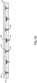
- the wafer chuck 102 may include a plurality of vacuum elements 105, as depicted in FIG. 1B .
- the plurality of vacuum elements 105 may generate one or more reduced pressure regions 109 distributed across the surface of the wafer chuck 102 suitable for securing the wafer 104 above the surface of the wafer chuck 102.
- the reduced pressure regions 109 are not necessarily formed in a one-to-one correspondence with the vacuum elements 105.
- two or more vacuum elements 105 may contribute to form a single reduced pressure region 109.
- some amount of "cross-flow" may exist between the pressurized gas regions 107 and the reduced pressure regions 109.
- gas from the pressurize gas elements 103 associated with regions 107 may flow to the reduced pressure regions 109 and be evacuated by the vacuum elements 105.
- the one or more pressurized gas elements 103 include one or more gas nozzles.
- the one or more pressurized gas elements 103 may include, but are not limited to, one or more gas nozzles configured to direct gas (e.g., air) upward from the surface of the wafer chuck 104 in order to generate the one or more pressurized regions 10.
- a pressurized gas nozzle may include, but is not limited to, a bore hole machined out of the surface (or molded/cast into the surface) of the wafer chuck 102, with one or more gas delivery lines fluidically coupled to the hole, which serve to deliver gas (e.g., air) to the hole.
- the one or more pressurized gas elements 103 include one or more gas channels.
- the one or more pressurized gas elements 103 may include, but are not limited to, one or more gas channels configured to direct gas (e.g., air) upward from the surface of the wafer chuck 104 in order to generate the one or more pressurized regions 107.
- a pressurized gas channel may include, but is not limited to, a recessed region machined out of the surface of the wafer chuck 102, with one or more gas delivery lines fluidically coupled to the recess, which serve to deliver gas (e.g., air) to the recessed channel.
- the one or more vacuum elements 105 include one or more gas nozzles.
- the one or more vacuum elements 105 may include, but are not limited to, one or more gas nozzles configured to evacuate gas (e.g., air) downward from the surface of the wafer chuck 104 in order to generate the one or more reduced pressure regions 109.
- a vacuum nozzle may include, but is not limited to, a bore hole machined out of the surface (or molded/cast into the surface) of the wafer chuck 102, with one or more gas delivery lines fluidically coupled to the hole, which serve to evacuate gas (e.g., air) from the region near the hole.
- the one or more vacuum elements 105 include one or more gas channels.
- the one or more vacuum elements 105 may include, but are not limited to, one or more gas channels configured to evacuate gas (e.g., air) downward from the surface of the wafer chuck 104 in order to generate the one or more reduced pressure regions 109.
- a vacuum gas channel may include, but is not limited to, a recessed region machined out of the surface of the wafer chuck 102, with gas delivery lines fluidically coupled to the recess, which serve to evacuate gas (e.g., air) from the region near the recessed channel.
- the vacuum elements 105 are interleaved with a portion pressurized gas elements 103.
- one or more vacuum elements 105 may be arranged so as to alternate with one or more of the pressurized gas elements 103. It is recognized herein that the pressurized gas elements 103 and the vacuum gas elements 105 may be arranged in any pattern across the surface of the wafer chuck 102. For example, the pressurized gas elements 103 and the vacuum gas element 105 may be arranged in any geometric pattern (or patterns) known in the art.
- the pressurized gas elements 103 and the vacuum gas elements 105 may be arranged in a linear grid, where one or more vacuum elements 105 are alternated, as function of X-Y position, with one or more pressurized gas elements 103.
- the pressurized gas elements 103 and the vacuum gas elements 105 may be arranged in a circular grid, where one or more vacuum gas elements 105 are alternated, as a function of angular position about the wafer chuck 102, with the one or more pressurized gas elements 103.
- the pressurized gas elements 103 and the vacuum elements 105 may be arranged in a concentric radial grid, where concentric rings of one or more vacuum gas elements 105 are alternated, as a function of radial position on the wafer chuck 102, with concentric rings of one or more pressurized gas elements 103.
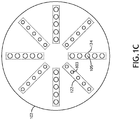
- FIG. 1C illustrates an arrangement of pressurized gas elements 103 and vacuum elements 105, in accordance with one embodiment of the present disclosure.
- the wafer chuck 102 includes multiple sets 122 of pressurized gas elements 103.
- the wafer chuck 102 includes multiple sets 124 of vacuum gas elements 105.
- the sets 122 of pressurized gas elements 103 may be interleaved with the sets 124 of vacuum elements 105. It is noted herein that the arrangement depicted in FIG. 1C is not limiting and is provided merely for illustrative purposes. It is again recognized that the pressurized gas elements (or sets of pressurized gas elements) and the vacuum elements (or sets of pressurized gas elements) may be arranged across the surface of the wafer chuck in any suitable pattern.
- the one or more pressurized gas elements 103 may be in fluidic communication with a gas delivery system and/or network (not shown).
- a gas source may be coupled to the delivery system/network, with gas being delivered to the pressurized gas elements 103 via the delivery system/network.
- the delivery system/network may include one or more gas pumps for pumping gas, such as air, to the pressurized gas elements 103.
- the delivery system/network may include one or more gas filters, such as an air filter, in order to filter the given gas prior to it being outputted through the pressurized gas elements 103.
- the one or more vacuum elements 105 may be in fluidic communication with a vacuum system and/or network (not shown).
- a gas pump may be fluidically coupled to the vacuum elements 105 and configured to evacuate gas through the vacuum elements 105 and to an external reservoir (e.g., gas container, ambient atmosphere and the like).
- an external reservoir e.g., gas container, ambient atmosphere and the like.
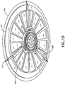
- FIG. 1D illustrates a schematic bottom view of the wafer chuck 102 and gripper assembly 106, in accordance with one or more embodiments of the present disclosure.
- the gripper elements 108 of the gripper assembly 106 act to laterally secure the wafer 104.
- the cam unit 114 is mechanically coupled to the wafer chuck 102 and is used to drive the motion of the gripper elements 108 in securing the wafer 104.
- the gripper elements of the gripper assembly 106 rotate the wafer 104 synchronously with the wafer chuck 102 as the wafer chuck 102 is rotated by the rotation drive unit 114 (not shown in FIG. 1D ).
- FIG. 1D illustrates a schematic bottom view of the wafer chuck 102 and gripper assembly 106, in accordance with one or more embodiments of the present disclosure.
- the gripper elements 108 of the gripper assembly 106 act to laterally secure the wafer 104.
- the cam unit 114 is mechanically coupled to the wafer chuck 102
- the wafer chuck 102 may include a set rows, aligned radially, of pressurized gas elements 103.
- the wafer chuck 102 may include a set of rows, aligned radially, of vacuum elements 105.
- the gripper assembly 106 is mechanically coupled to a portion the wafer chuck 102.
- the gripper assembly 106 is reversibly couplable to one or more edge portions of the wafer 104.
- the gripper assembly 106 may laterally secure the wafer 104.
- the gripper assembly 106 may serve to secure the wafer 104 along the horizontal direction without applying a significant contact force in the vertical direction.
- the gripper assembly 106 may laterally and rotationally secure (relative to the wafer chuck 102) the wafer 104 such that when the wafer chuck 102 and the gripper assembly 106 are rotated by the rotational drive unit 116 the wafer 104 is also rotated.
- the wafer 104 rotates relative to an outside reference frame, the wafer 104 does not move significantly with respect to the surface of the wafer chuck 102 during a wafer scanning process.
- the gripper assembly 106 may serve to adjust the lateral position of the wafer 104 in order to substantially center the wafer 104 prior to rotation of the wafer 104 during a scanning process.
- the gripper assembly 106 of the wafer chucking system 100 includes one or more gripper elements 108.
- the gripper elements 108 of the gripper assembly 106 include one or more connection arms, or rods, 110 and one or more gripper heads 112.
- the one or more gripper heads 112 may include any mechanism known in the art suitable for securing the wafer 104.
- the one or more gripper heads 112 may include, but is not limited to, a spring loaded device for securing the wafer.
- the one or more gripper heads 112 may include, but is not limited to, a frictional portion configured to secure the wafer 104 via friction.
- the gripper assembly 106 may include, but is not limited to, two or more gripper elements 108 (e.g., 2, 3, 4, 5 and so on).
- the gripper assembly 106 may include three gripper elements 108.
- the gripper assembly 106 may include four gripper elements 108.
- the gripper assembly 106 includes a cam unit 114.
- the cam unit 114 is mechanically coupled to the gripper assembly 106.
- the cam unit is configured to drive the linear motion of one or more gripper elements 108 of the gripper assembly 106.
- the cam unit 114 may selectably engage and/or disengage the gripper elements 108 with one or more portions of the wafer 104.
- the cam unit 114 may cause the gripper elements 108 to move into an expanded, or disengaged, state.
- Such a configuration allows for a user (or robotic arm) to load a wafer 104 onto the wafer chuck 102 prior to a rotational scanning process.
- the cam unit 114 may be placed in a disengaged state when the user or robotic arm (not shown) unloads the wafer 104 from the chuck 102.
- the cam unit 114 may cause the gripper elements 108 to move into a retracted, or engaged state.
- Such a configuration serves to laterally secure the wafer 102, while the chuck 102 secures the wafer above the chuck 102, during a rotational scanning process.
- the wafer chuck 102 (and the connected gripper assembly 106) are supported by a shaft 116, or spindle, of the rotational drive unit 117.
- the shaft 117 may be connected to a motor 119.
- the motor 119 may be configured to rotate the shaft 117 at a selected rotational velocity, thereby rotating the wafer chuck 102, the gripper assembly 106 and the wafer 104 about an axis perpendicular to the surface of the wafer chuck 102.
- the wafer chuck 102, the gripper assembly 106 and the wafer 104 may be rotated at speeds greater than 1,000 revolutions per minute (rpm) (e.g., 1,000 to 10,000 rpm).
- FIGS. 2A and 2B illustrate high-level block diagram views of inspection systems 200, 210 equipped with the non-contact wafer chucking system 100, in accordance with one or more embodiments of the present disclosure.
- the wafer inspection systems 200, 210 of the present disclosure may include the non-contact wafer chucking system 100, as described previously herein.
- the inspection systems 200, 210 further include least one light source 202 (e.g., one or more lasers, one or more broadband light sources and etc.) configured to illuminate an area on the surface of the wafer 104.
- the inspection systems 200, 210 include one or more detectors 204, or cameras, suitable for detecting light reflected, diffracted or scattered from the area illuminated by the light source 202.
- the one or more detectors 204 may include, but are not limited to, a CCD or TDI-CCD detector, or a photomultiplier detector.
- the inspection systems 200, 210 may include a set of optical elements (e.g., illumination optics, collection optics, beam splitters 206, filters and the like) configured for directing (and focusing) illumination from the light source 202 onto the surface of the wafer 104 and, in turn, directing illumination from the surface of the wafer 104 to the imaging portion of the detector 204 of the inspection systems 200, 210.
- optical elements e.g., illumination optics, collection optics, beam splitters 206, filters and the like
- the set of optical elements for the systems 200, 210 may include, but is not limited to, a primary imaging lens suitable for imaging the illuminated area of the wafer onto a collection portion(s) of the detector 204.
- the imaging detector 204 may be communicatively coupled to an image processing computer which may identify and store imagery data acquired from the detector 204.
- the inspection systems 200, 210 of the present disclosure may be configured as any inspection system known in the art.
- the inspection system 200 of the present invention may be configured as a bright field (BF) inspection system.
- the inspection system 210 may be configured as a dark field (DF) inspection system.
- BF bright field
- DF dark field
- the inspection systems 200, 210 of the present disclosure may include any set of imaging and optical elements suitable for imaging the surface of the wafer 104. Examples of wafer inspection tools are described in detail in U.S. Pat. No. 7,092,082 , U.S. Pat. No. 6,702,302 , U.S. Pat. No. 6,621,570 and U.S. Pat. No. 5,805,278 .
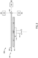
- FIG. 3 illustrate high-level block diagram views of an edge inspection 300 equipped with the non-contact wafer chucking system 100, in accordance with one or more embodiments of the present disclosure.
- an edge inspection system 300 may include a detector 304 suitable for collecting imagery data from the edge region 302 of the wafer 104. It is further recognized that the inspection system 300 allows for various portions of the edge 302 to be inspected using the detector 304. For example, as shown in FIG.
- the detector 304 may collect imagery data at a location A at the top portion of the edge 302 of the wafer 104 (e.g., top portion of wafer bevel).
- the detector 304 may collect imagery data at a location B at the center portion of the edge 302 of the wafer 104 (e.g., center of wafer bevel).
- the detector 304 may collect imagery data at a location C at the bottom portion of the edge 302 of the wafer 104 (e.g., bottom portion of wafer bevel).
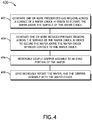
- FIG 4 illustrates a flow diagram depicting the steps of a method 400 for non-contact chucking of a wafer, in accordance with one or more embodiments of the present disclosure.
- step 402 one or more pressurized gas regions are generated across a surface of a wafer chuck in order to elevate the wafer above the surface of the wafer chuck.
- step 404 one or more reduced pressure regions are generated across the surface of the wafer chuck in order to secure the wafer above the wafer chuck without contact to the wafer chuck.
- one or more gripper elements are reversibly coupled, or attached, to an edge portion of the wafer in order to rotationally secure the wafer with respect to the wafer chuck.
- step 408 the wafer, the plurality of gripper elements and the wafer chuck are synchronously rotated at a selected rotational velocity.
- any two components herein combined to achieve a particular functionality can be seen as “associated with” each other such that the desired functionality is achieved, irrespective of architectures or intermedial components.
- any two components so associated can also be viewed as being “connected”, or “coupled”, to each other to achieve the desired functionality, and any two components capable of being so associated can also be viewed as being “couplable”, to each other to achieve the desired functionality.
- Specific examples of couplable include but are not limited to physically mateable and/or physically interacting components and/or wirelessly interactable and/or wirelessly interacting components and/or logically interacting and/or logically interactable components.
Landscapes
- Immunology (AREA)
- Pathology (AREA)
- Life Sciences & Earth Sciences (AREA)
- Chemical & Material Sciences (AREA)
- Analytical Chemistry (AREA)
- Biochemistry (AREA)
- Health & Medical Sciences (AREA)
- General Health & Medical Sciences (AREA)
- Physics & Mathematics (AREA)
- General Physics & Mathematics (AREA)
- Container, Conveyance, Adherence, Positioning, Of Wafer (AREA)
- Testing Or Measuring Of Semiconductors Or The Like (AREA)
- Investigating Materials By The Use Of Optical Means Adapted For Particular Applications (AREA)
- Length Measuring Devices By Optical Means (AREA)
- Engineering & Computer Science (AREA)
- Mechanical Engineering (AREA)
Description
- The present application claims the benefit under 35 U.S.C. § 119(e) of
U.S. Provisional Application Serial Number 61/920,456, filed December 23, 2013 - The present invention generally relates to a wafer chuck for use in a wafer characterization system and, in particular, to a non-contact wafer chuck.
- As tolerances on semiconductor device fabrication processes continue to narrow, the demand for improved semiconductor wafer review tools continues to increase. One such review tool includes a wafer inspection tool, such as a wafer edge inspection tool. In such an optical system, an associated wafer chuck may be used to rotate the wafer during edge inspection. Some wafer chucks may provide an air bearing that elevates the wafer above the wafer chuck surface. Such systems, however, suffer from height variations associated with the wafer chuck as the wafer is rotated with respect to the underlying wafer chuck. Therefore, it would be advantageous to provide a system and method that cures the defects identified in the previous art.
-
US2007195653 discloses an apparatus for supporting a stationary or moving substantially flat object without physical contact on an fluid-cushion. The object floats on a fluid cushion gap, the apparatus aimed for globally or locally adjusting the gap. - An apparatus for non-contact chucking a wafer is disclosed, in accordance with an illustrative embodiment of the present invention. In one illustrative embodiment, the apparatus includes a wafer chuck. In one illustrative embodiment, the wafer chuck includes one or more pressurized gas elements configured to generate one or more pressurized gas regions across a surface of the wafer chuck suitable for elevating the wafer above the surface of the wafer chuck. In another illustrative embodiment, the wafer chuck further includes one or more vacuum elements configured to generate one or more reduced pressure regions across the surface of the wafer chuck. In one illustrative embodiment, the reduced pressure regions have a pressure lower than the pressurized gas regions. In another illustrative embodiment, the one or more reduced pressure regions are suitable for securing the wafer above the wafer chuck without contact to the wafer chuck. In another illustrative embodiment, the apparatus includes a gripper assembly coupled to a portion of the wafer chuck, wherein the gripper assembly includes a plurality of gripper elements. In another illustrative embodiment, the apparatus includes a rotational drive unit mechanically coupled to the wafer chuck. In another illustrative embodiment, the rotational drive unit is configured to selectively rotate the wafer chuck. In another illustrative embodiment, the gripper assembly includes a cam unit coupled to the gripper assembly, wherein the cam unit is configured to drive one or more of the gripper elements along a radial direction of the wafer chuck so as to selectably engage the gripper assembly with one or more edge portions of the wafer so as to secure the wafer such that the wafer and the gripper assembly rotate synchronously with the wafer chuck during rotation of the wafer chuck by the rotational drive unit.
- An optical system is disclosed, in accordance with an illustrative embodiment of the present invention. In one illustrative embodiment, the optical system includes a wafer chucking sub-system. In another illustrative embodiment, the optical system includes an illumination source configured to illuminate one or more portions of the wafer secured by the wafer chucking sub-system. In another illustrative embodiment, the optical system includes a detector configured to collect illumination from the illuminated one or more portions of the wafer. In one illustrative embodiment, wafer chucking sub-system includes a wafer chuck. In one illustrative embodiment, the wafer chuck includes one or more pressurized gas elements configured to generate one or more pressurized gas regions across a surface of the wafer chuck suitable for elevating the wafer above the surface of the wafer chuck. In another illustrative embodiment, the wafer chuck further includes one or more vacuum elements configured to generate one or more reduced pressure regions across the surface of the wafer chuck. In one illustrative embodiment, the reduced pressure regions have a pressure lower than the pressurized gas regions. In another illustrative embodiment, the one or more reduced pressure regions are suitable for securing the wafer above the wafer chuck without contact to the wafer chuck. In another illustrative embodiment, the wafer chucking sub-system includes a gripper assembly coupled to a portion of the wafer chuck, wherein the gripper assembly includes a plurality of gripper elements. In another illustrative embodiment, the wafer chucking sub-system includes a rotational drive unit mechanically coupled to the wafer chuck. In another illustrative embodiment, the rotational drive unit is configured to selectively rotate the wafer chuck. In another illustrative embodiment, the gripper assembly includes a cam unit coupled to the gripper assembly, wherein the cam unit is configured to drive one or more of the gripper elements along a radial direction of the wafer chuck so as to selectably engage the gripper assembly with one or more edge portions of the wafer so as to secure the wafer such that the wafer and the gripper assembly rotate synchronously with the wafer chuck during rotation of the wafer chuck by the rotational drive unit.
- An apparatus for non-contact chucking of a wafer is disclosed, in accordance with an illustrative embodiment of the present invention. In one illustrative embodiment, the method includes generating one or more pressurized gas regions across a surface of a wafer chuck in order to elevate the wafer above the surface of the wafer chuck. In another illustrative embodiment, the method includes generating one or more reduced pressure regions across the surface of the wafer chuck in order to secure the wafer above the wafer chuck without contact to the wafer chuck. In another illustrative embodiment, the method includes reversibly coupling a gripper assembly to an edge portion of the wafer in order to rotationally secure the wafer with respect to the wafer chuck. In another illustrative embodiment, the method includes synchronously rotating the wafer, gripper assembly and the wafer chuck at a selected rotational velocity.
- It is to be understood that both the foregoing general description and the following detailed description are exemplary and explanatory only and are not necessarily restrictive of the invention as claimed. The accompanying drawings, which are incorporated in and constitute a part of the specification, illustrate embodiments of the invention and together with the general description, serve to explain the principles of the invention.
- The numerous advantages of the disclosure may be better understood by those skilled in the art by reference to the accompanying figures in which:
-
FIG. 1A is a cross-sectional view of a non-contact wafer chucking system, in accordance with one embodiment of the present disclosure. -
FIG. 1B is a cross-sectional view of a wafer chuck of a non-contact wafer chucking system, in accordance with one embodiment of the present disclosure. -
FIG. 1C is a top view of a wafer chuck of a non-contact wafer chucking system, in accordance with one embodiment of the present disclosure. -
FIG. 1D is a schematic bottom view of a non-contact wafer chucking system, in accordance with one embodiment of the present disclosure. -
FIG. 1E is a schematic top view of a non-contact wafer chucking system, in accordance with one embodiment of the present disclosure. -
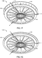
FIG. 1F is a schematic bottom view of a non-contact wafer chucking system having a gripper assembly in a disengaged state, in accordance with one embodiment of the present disclosure. -
FIG. 1G is a schematic bottom view of a non-contact wafer chucking system having a gripper assembly in an engaged state, in accordance with one embodiment of the present disclosure. -
FIG. 2A is a simplified schematic view of a wafer inspection system equipped with a non-contact wafer chucking system, in accordance with one embodiment of the present disclosure. -
FIG. 2B is a simplified schematic view of a wafer inspection system equipped with a non-contact wafer chucking system, in accordance with one embodiment of the present disclosure. -
FIG. 3 is a simplified schematic view of a wafer edge inspection system equipped with a non-contact wafer chucking system, in accordance with one embodiment of the present disclosure. -
FIG. 4 is flow diagram of depicting a method for non-contact chucking of a wafer, in accordance with one embodiment of the present disclosure. - Reference will now be made in detail to the subject matter disclosed, which is illustrated in the accompanying drawings.
- Referring generally to
FIGS. 1A through 4 , a system and method for non-contact chucking of a wafer is described in accordance with the present disclosure. The use of a non-contact wafer chuck is described generally inU.S. Patent No. 8,444,126 to Siebert et al., issued on May 21, 2013 . - Embodiments of the present disclosure are directed to a wafer chuck and gripping device suitable for elevating and securing a wafer, such as a semiconductor wafer (e.g., 200 to 500 mm wafer), above the wafer chuck. Embodiments of the present disclosure are further directed to rotating the wafer and wafer chuck synchronously such that during a given scan there is no relative emotion between the wafer and the wafer chuck. Such a configuration aids in avoiding scanning errors caused by height variation and vibration of the wafer chuck. It is further noted that the wafer chucking system of the present disclosure may be implemented in a variety of optical measurement contexts, such as, but not limited to, a wafer edge inspection system.
-
FIG. 1A illustrates a simplified cross-sectional view of a non-contactwafer chucking system 100, in accordance with one embodiment of the present disclosure. In one embodiment, thewafer chucking system 100 includes awafer chuck 100 for securing awafer 104 above the surface of thewafer chuck 102 without making contact with thewafer chuck 102. In another embodiment, thewafer chucking system 100 includesgripper assembly 106. In another embodiment, thewafer chucking system 100 includes arotational drive unit 116. Therotational drive unit 116 is coupled to thewafer chuck 102 and configured to selectably rotate thewafer chuck 102, thegripper assembly 106 and thewafer 104 during a wafer scanning process. - In one embodiment, as shown in
FIGS. 1A-1B , thewafer chuck 102 includes one or morepressurized gas elements 103. In one embodiment, apressurized gas element 103 generates an associatedpressurized region 107 at or near the output of the respectivepressurized gas element 103. Thepressurized region 107 serves to provide an upward force on thewafer 104. In this regard, the one or one or morepressurized gas elements 103 may generate one or morepressurized gas regions 107 across a surface of thewafer chuck 102 suitable for elevating thewafer 104 above the surface of thewafer chuck 102. In one embodiment, thewafer chuck 102 may include a plurality ofpressurized gas elements 103, as depicted inFIG. 1B . In this regard, the plurality ofpressurized gas elements 103 may generate one or morepressurized gas regions 107 distributed across the surface of the wafer chuck suitable for elevating thewafer 104 above the surface of thewafer chuck 102. It is noted herein that thepressurized gas regions 107 are not necessarily formed in a one-to-one correspondence with thepressurized gas elements 103. For example, two or more gas elements 103 (e.g., gas nozzles, gas channels, multiple gas nozzles, multiple gas channels) may contribute to form a singlepressurized gas region 107. - In one embodiment, the one or more
pressurized elements 103 of thewafer chuck 102 form a pressurized air pocket for elevating thewafer 104 above the surface of thewafer chuck 102. In this regard, the one or morepressurized elements 103 may form one or more pressurized air pockets (or other gas), which exerts a net upward force on the bottom of thewafer 104, thereby causing thewafer 104 to stabilize vertically at some location above thewafer chuck 104. - In another embodiment, as shown in
FIGS. 1A-B , thewafer chuck 102 includes one ormore vacuum elements 105. In one embodiment, avacuum element 105 generates an associated reduced pressure, or vacuum,region 109 at or near the input of the respectivevacuum gas element 105. For example, the one or morereduced pressure regions 109 may have a pressure that is lower than the one or morepressurized regions 107. The one ormore vacuum elements 105 may generate one or morereduced pressure regions 109 across a surface of thewafer chuck 102 suitable for securing thewafer 104 above the surface of thewafer chuck 102 without contact taking place between thewafer 104 and thewafer chuck 102. In this regard, the reducedpressure regions 109 serve to provide a downward force on thewafer 104. The combination of the downward forced from thevacuum elements 105 and the upward force from the one or more pressurized gas elements serves to stabilize the vertical position of thewafer 102 at some location above thewafer chuck 102. - In one embodiment, the
wafer chuck 102 may include a plurality ofvacuum elements 105, as depicted inFIG. 1B . In this regard, the plurality ofvacuum elements 105 may generate one or morereduced pressure regions 109 distributed across the surface of thewafer chuck 102 suitable for securing thewafer 104 above the surface of thewafer chuck 102. It is noted herein that the reducedpressure regions 109 are not necessarily formed in a one-to-one correspondence with thevacuum elements 105. For example, two ormore vacuum elements 105 may contribute to form a single reducedpressure region 109. It is further noted herein that some amount of "cross-flow" may exist between thepressurized gas regions 107 and the reducedpressure regions 109. In this regard, gas from thepressurize gas elements 103 associated withregions 107 may flow to the reducedpressure regions 109 and be evacuated by thevacuum elements 105. - In one embodiment, the one or more
pressurized gas elements 103 include one or more gas nozzles. For example, the one or morepressurized gas elements 103 may include, but are not limited to, one or more gas nozzles configured to direct gas (e.g., air) upward from the surface of thewafer chuck 104 in order to generate the one or more pressurized regions 10. For instance, a pressurized gas nozzle may include, but is not limited to, a bore hole machined out of the surface (or molded/cast into the surface) of thewafer chuck 102, with one or more gas delivery lines fluidically coupled to the hole, which serve to deliver gas (e.g., air) to the hole. - In one embodiment, the one or more
pressurized gas elements 103 include one or more gas channels. For example, the one or morepressurized gas elements 103 may include, but are not limited to, one or more gas channels configured to direct gas (e.g., air) upward from the surface of thewafer chuck 104 in order to generate the one or morepressurized regions 107. For instance, a pressurized gas channel may include, but is not limited to, a recessed region machined out of the surface of thewafer chuck 102, with one or more gas delivery lines fluidically coupled to the recess, which serve to deliver gas (e.g., air) to the recessed channel. - In one embodiment, the one or
more vacuum elements 105 include one or more gas nozzles. For example, the one ormore vacuum elements 105 may include, but are not limited to, one or more gas nozzles configured to evacuate gas (e.g., air) downward from the surface of thewafer chuck 104 in order to generate the one or morereduced pressure regions 109. For instance, a vacuum nozzle may include, but is not limited to, a bore hole machined out of the surface (or molded/cast into the surface) of thewafer chuck 102, with one or more gas delivery lines fluidically coupled to the hole, which serve to evacuate gas (e.g., air) from the region near the hole. - In one embodiment, the one or
more vacuum elements 105 include one or more gas channels. For example, the one ormore vacuum elements 105 may include, but are not limited to, one or more gas channels configured to evacuate gas (e.g., air) downward from the surface of thewafer chuck 104 in order to generate the one or morereduced pressure regions 109. For instance, a vacuum gas channel may include, but is not limited to, a recessed region machined out of the surface of thewafer chuck 102, with gas delivery lines fluidically coupled to the recess, which serve to evacuate gas (e.g., air) from the region near the recessed channel. - In one embodiment, as shown in
FIG. 1B , at least a portion of thevacuum elements 105 are interleaved with a portion pressurizedgas elements 103. In this regard, one ormore vacuum elements 105 may be arranged so as to alternate with one or more of thepressurized gas elements 103. It is recognized herein that thepressurized gas elements 103 and thevacuum gas elements 105 may be arranged in any pattern across the surface of thewafer chuck 102. For example, thepressurized gas elements 103 and thevacuum gas element 105 may be arranged in any geometric pattern (or patterns) known in the art. - For instance, the
pressurized gas elements 103 and thevacuum gas elements 105 may be arranged in a linear grid, where one ormore vacuum elements 105 are alternated, as function of X-Y position, with one or morepressurized gas elements 103. In another instance, thepressurized gas elements 103 and thevacuum gas elements 105 may be arranged in a circular grid, where one or morevacuum gas elements 105 are alternated, as a function of angular position about thewafer chuck 102, with the one or morepressurized gas elements 103. In another instance, thepressurized gas elements 103 and thevacuum elements 105 may be arranged in a concentric radial grid, where concentric rings of one or morevacuum gas elements 105 are alternated, as a function of radial position on thewafer chuck 102, with concentric rings of one or morepressurized gas elements 103. -
FIG. 1C illustrates an arrangement ofpressurized gas elements 103 andvacuum elements 105, in accordance with one embodiment of the present disclosure. In one embodiment, thewafer chuck 102 includesmultiple sets 122 ofpressurized gas elements 103. In another embodiment, thewafer chuck 102 includesmultiple sets 124 ofvacuum gas elements 105. As shown inFIG. 1C , thesets 122 ofpressurized gas elements 103 may be interleaved with thesets 124 ofvacuum elements 105. It is noted herein that the arrangement depicted inFIG. 1C is not limiting and is provided merely for illustrative purposes. It is again recognized that the pressurized gas elements (or sets of pressurized gas elements) and the vacuum elements (or sets of pressurized gas elements) may be arranged across the surface of the wafer chuck in any suitable pattern. - It is noted herein that the one or more
pressurized gas elements 103 may be in fluidic communication with a gas delivery system and/or network (not shown). In this regard, a gas source may be coupled to the delivery system/network, with gas being delivered to thepressurized gas elements 103 via the delivery system/network. In one embodiment, the delivery system/network may include one or more gas pumps for pumping gas, such as air, to thepressurized gas elements 103. In another embodiment, the delivery system/network may include one or more gas filters, such as an air filter, in order to filter the given gas prior to it being outputted through thepressurized gas elements 103. It is further noted herein that the one ormore vacuum elements 105 may be in fluidic communication with a vacuum system and/or network (not shown). In this regard, a gas pump may be fluidically coupled to thevacuum elements 105 and configured to evacuate gas through thevacuum elements 105 and to an external reservoir (e.g., gas container, ambient atmosphere and the like). Those skilled in the art should recognize that there are a variety of gas delivery and gas vacuum mechanisms suitable for implementation in thesystem 100 of the present disclosure. -
FIG. 1D illustrates a schematic bottom view of thewafer chuck 102 andgripper assembly 106, in accordance with one or more embodiments of the present disclosure. As shown inFIG. 1D , thegripper elements 108 of thegripper assembly 106 act to laterally secure thewafer 104. Further, thecam unit 114 is mechanically coupled to thewafer chuck 102 and is used to drive the motion of thegripper elements 108 in securing thewafer 104. Once secure, the gripper elements of thegripper assembly 106 rotate thewafer 104 synchronously with thewafer chuck 102 as thewafer chuck 102 is rotated by the rotation drive unit 114 (not shown inFIG. 1D ).FIG. 1E illustrates a schematic top view of thewafer chuck 102 securing thewafer 104, in accordance with one or more embodiments of the present disclosure. As shown inFIG. 1E , thewafer chuck 102 may include a set rows, aligned radially, ofpressurized gas elements 103. In addition, thewafer chuck 102 may include a set of rows, aligned radially, ofvacuum elements 105. - Referring again to
FIG. 1A , in one embodiment, thegripper assembly 106 is mechanically coupled to a portion thewafer chuck 102. In one embodiment, thegripper assembly 106 is reversibly couplable to one or more edge portions of thewafer 104. In this regard, thegripper assembly 106 may laterally secure thewafer 104. For example, as shown inFIG. 1A , thegripper assembly 106 may serve to secure thewafer 104 along the horizontal direction without applying a significant contact force in the vertical direction. In another embodiment, thegripper assembly 106 may laterally and rotationally secure (relative to the wafer chuck 102) thewafer 104 such that when thewafer chuck 102 and thegripper assembly 106 are rotated by therotational drive unit 116 thewafer 104 is also rotated. In this regard, while thewafer 104 rotates relative to an outside reference frame, thewafer 104 does not move significantly with respect to the surface of thewafer chuck 102 during a wafer scanning process. - In another embodiment, the
gripper assembly 106 may serve to adjust the lateral position of thewafer 104 in order to substantially center thewafer 104 prior to rotation of thewafer 104 during a scanning process. - In one embodiment, the
gripper assembly 106 of thewafer chucking system 100 includes one or moregripper elements 108. In another embodiment, thegripper elements 108 of thegripper assembly 106 include one or more connection arms, or rods, 110 and one or more gripper heads 112. In another embodiment, the one or more gripper heads 112 may include any mechanism known in the art suitable for securing thewafer 104. For example, the one or more gripper heads 112 may include, but is not limited to, a spring loaded device for securing the wafer. By way of another example, the one or more gripper heads 112 may include, but is not limited to, a frictional portion configured to secure thewafer 104 via friction. - In one embodiment, the
gripper assembly 106 may include, but is not limited to, two or more gripper elements 108 (e.g., 2, 3, 4, 5 and so on). For example, as shown inFIG. 1D and1E , thegripper assembly 106 may include threegripper elements 108. In another instance, although not shown, thegripper assembly 106 may include fourgripper elements 108. - In another embodiment, the
gripper assembly 106 includes acam unit 114. In one embodiment, thecam unit 114 is mechanically coupled to thegripper assembly 106. In one embodiment, as shown inFIGS. 1F and 1G , the cam unit is configured to drive the linear motion of one or moregripper elements 108 of thegripper assembly 106. In this regard, thecam unit 114 may selectably engage and/or disengage thegripper elements 108 with one or more portions of thewafer 104. For example, as shown inFIG. 1F , thecam unit 114 may cause thegripper elements 108 to move into an expanded, or disengaged, state. Such a configuration allows for a user (or robotic arm) to load awafer 104 onto thewafer chuck 102 prior to a rotational scanning process. In addition, thecam unit 114 may be placed in a disengaged state when the user or robotic arm (not shown) unloads thewafer 104 from thechuck 102. By way of further example, as shown inFIG. 1G , thecam unit 114 may cause thegripper elements 108 to move into a retracted, or engaged state. Such a configuration serves to laterally secure thewafer 102, while thechuck 102 secures the wafer above thechuck 102, during a rotational scanning process. - Referring again to
FIG. 1A , the wafer chuck 102 (and the connected gripper assembly 106) are supported by ashaft 116, or spindle, of therotational drive unit 117. For example, theshaft 117 may be connected to amotor 119. In this regard, themotor 119 may be configured to rotate theshaft 117 at a selected rotational velocity, thereby rotating thewafer chuck 102, thegripper assembly 106 and thewafer 104 about an axis perpendicular to the surface of thewafer chuck 102. For instance, thewafer chuck 102, thegripper assembly 106 and thewafer 104 may be rotated at speeds greater than 1,000 revolutions per minute (rpm) (e.g., 1,000 to 10,000 rpm). -
FIGS. 2A and 2B illustrate high-level block diagram views ofinspection systems wafer chucking system 100, in accordance with one or more embodiments of the present disclosure. In one embodiment, thewafer inspection systems wafer chucking system 100, as described previously herein. In one embodiment, theinspection systems wafer 104. In another embodiment, theinspection systems more detectors 204, or cameras, suitable for detecting light reflected, diffracted or scattered from the area illuminated by thelight source 202. In one embodiment, the one ormore detectors 204 may include, but are not limited to, a CCD or TDI-CCD detector, or a photomultiplier detector. In addition, theinspection systems beam splitters 206, filters and the like) configured for directing (and focusing) illumination from thelight source 202 onto the surface of thewafer 104 and, in turn, directing illumination from the surface of thewafer 104 to the imaging portion of thedetector 204 of theinspection systems systems detector 204. Further, theimaging detector 204 may be communicatively coupled to an image processing computer which may identify and store imagery data acquired from thedetector 204. - The
inspection systems FIG. 2A , theinspection system 200 of the present invention may be configured as a bright field (BF) inspection system. Alternatively, as shown inFIG. 2B , theinspection system 210 may be configured as a dark field (DF) inspection system. Applicant notes that the optical configurations depicted inFIGS. 2A and 2B are provided merely for illustrative purposes and should not be interpreted as limiting. In a general sense, theinspection systems wafer 104. Examples of wafer inspection tools are described in detail inU.S. Pat. No. 7,092,082 ,U.S. Pat. No. 6,702,302 ,U.S. Pat. No. 6,621,570 andU.S. Pat. No. 5,805,278 . -
FIG. 3 illustrate high-level block diagram views of anedge inspection 300 equipped with the non-contactwafer chucking system 100, in accordance with one or more embodiments of the present disclosure. For purposes of clarity, thegripper assembly 106 is not depicted inFIG. 3 , even though it is recognized herein that thegripper assembly 106 is present in such an edge inspection setting. As shown inFIG. 3 , anedge inspection system 300 may include adetector 304 suitable for collecting imagery data from theedge region 302 of thewafer 104. It is further recognized that theinspection system 300 allows for various portions of theedge 302 to be inspected using thedetector 304. For example, as shown inFIG. 3 , thedetector 304 may collect imagery data at a location A at the top portion of theedge 302 of the wafer 104 (e.g., top portion of wafer bevel). By way of another example, as shown inFIG. 3 , thedetector 304 may collect imagery data at a location B at the center portion of theedge 302 of the wafer 104 (e.g., center of wafer bevel). By way of another example, as shown inFIG. 3 , thedetector 304 may collect imagery data at a location C at the bottom portion of theedge 302 of the wafer 104 (e.g., bottom portion of wafer bevel). -
FIG 4 illustrates a flow diagram depicting the steps of amethod 400 for non-contact chucking of a wafer, in accordance with one or more embodiments of the present disclosure. Instep 402, one or more pressurized gas regions are generated across a surface of a wafer chuck in order to elevate the wafer above the surface of the wafer chuck. Instep 404, one or more reduced pressure regions are generated across the surface of the wafer chuck in order to secure the wafer above the wafer chuck without contact to the wafer chuck. Instep 406, one or more gripper elements are reversibly coupled, or attached, to an edge portion of the wafer in order to rotationally secure the wafer with respect to the wafer chuck. Instep 408, the wafer, the plurality of gripper elements and the wafer chuck are synchronously rotated at a selected rotational velocity. - The herein described subject matter sometimes illustrates different components contained within, or connected with, other components. It is to be understood that such depicted architectures are merely exemplary, and that in fact many other architectures can be implemented which achieve the same functionality. In a conceptual sense, any arrangement of components to achieve the same functionality is effectively "associated" such that the desired functionality is achieved. Hence, any two components herein combined to achieve a particular functionality can be seen as "associated with" each other such that the desired functionality is achieved, irrespective of architectures or intermedial components. Likewise, any two components so associated can also be viewed as being "connected", or "coupled", to each other to achieve the desired functionality, and any two components capable of being so associated can also be viewed as being "couplable", to each other to achieve the desired functionality. Specific examples of couplable include but are not limited to physically mateable and/or physically interacting components and/or wirelessly interactable and/or wirelessly interacting components and/or logically interacting and/or logically interactable components.
- It is believed that the present disclosure and many of its attendant advantages will be understood by the foregoing description, and it will be apparent that various changes may be made in the form, construction and arrangement of the components without departing from the disclosed subject matter or without sacrificing all of its material advantages. The form described is merely explanatory, and it is the intention of the following claims to encompass and include such changes. Furthermore, it is to be understood that the invention is defined by the appended claims.
Claims (14)
- An apparatus for non-contact chucking of a wafer (100) comprising:a wafer chuck (102), the wafer chuck (102) including one or more pressurized gas elements (103) configured to generate one or more pressurized gas regions (107) across a surface of the wafer chuck (102) suitable for elevating the wafer (104) above the surface of the wafer chuck (102), the wafer chuck (102) further including one or more vacuum elements (105) configured to generate one or more reduced pressure regions (109) across the surface of the wafer chuck (102), the reduced pressure regions (109) having a pressure lower than the pressurized gas regions (107), the one or more reduced pressure regions (109) suitable for securing the wafer (104) above the wafer chuck (102) without contact to the wafer chuck (102);a gripper assembly (106) coupled to a portion of the wafer chuck (102), wherein the gripper assembly (106) includes a plurality of gripper elements (108); anda rotational drive unit (117) mechanically coupled to the wafer chuck (102),wherein the rotational drive unit (117) is configured to selectively rotate the wafer chuck (102),characterized in that the gripper assembly (106) includes a cam unit (114), wherein the cam unit (114) is configured to drive one or more of the gripper elements (108) along a radial direction of the wafer chuck (102) so as to selectably engage the gripper assembly (106) with one or more edge portions of the wafer (104) so as to secure the wafer (104) such that the wafer (104) and the gripper assembly (106) rotate synchronously with the wafer chuck (102) during rotation of the wafer chuck (102) by the rotational drive unit (117).
- The apparatus of claim 1, wherein the one or more pressurized gas elements (103) comprise:(a) one or more pressurized gas nozzles configured to direct gas upward from the surface of the wafer chuck (102) in order to generate the one or more pressurized regions (107); or(b) one or more pressurized gas channels configured to direct gas upward from the surface of the wafer chuck (102) in order to generate the one or more pressurized regions (107); or(c) a plurality of pressurized gas elements.
- The apparatus of claim 1, wherein the one or more pressurized elements (103) of the wafer chuck (102) form a pressurized air pocket for elevating the wafer (104) above the surface of the wafer chuck (102).
- The apparatus of claim 1, wherein the one or more vacuum elements (105) comprise:(a) one or more vacuum nozzles configured to evacuate gas from the surface of the wafer chuck (102) in order to generate the one or more reduced pressure regions (109); or(b) one or more vacuum channels configured to evacuate gas from the surface of the wafer chuck in order to generate the one or more reduced pressure regions (109).
- The apparatus of claim 2 when dependent on option (c), wherein the one or more vacuum elements (105) comprise:a plurality of vacuum elements, ora plurality of vacuum elements, wherein at least some of the plurality of vacuum elements are interleaved with at least some of the plurality of pressurized gas elements (103).
- The apparatus of claim 1, wherein the one or more pressurized gas elements (103) comprise:
a plurality of sets of pressurized gas elements. - The apparatus of claim 6, wherein the one or more vacuum elements (105) comprise:
a plurality of sets of vacuum elements. - The apparatus of claim 7, wherein at least some of the plurality of sets of vacuum elements (105) are interleaved with at least some of the plurality of sets of pressurized gas elements (103).
- The apparatus of claim 1, wherein the one or more pressurized regions (107):(a) are proximate to the one or more reduced pressure regions (109); or(b) are adjacent to the one or more reduced pressure regions (109); or(c) alternate with the one or more reduced pressure regions (109).
- The apparatus of claim 1:wherein the plurality of gripper elements (108) comprises three or more gripper elements (108); orwherein at least some of the gripper elements (108) are couplable to an edge portion of the wafer (104).
- The apparatus of claim 1, wherein the gripper assembly (106) is configured to:(a) selectably disengage from the edge portion of the wafer (104); or(b) laterally position the wafer (104) on the wafer chuck (102).
- The apparatus of claim 1, wherein the rotational drive unit (117) comprises:a spindle; anda motor.
- An optical system (200, 210) comprising:a wafer chucking sub-system including an apparatus for non-contact chucking of a wafer (100) as claimed in claim 1; andan illumination source (202) configured to illuminate one or more portions of the wafer (104) secured by the wafer chucking sub-system (100); anda detector (204) configured to collect illumination from the illuminated one or more portions of the wafer (104).
- A method for non-contact chucking of a wafer (400) comprising:generating one or more pressurized gas regions across a surface of a wafer chuck (402) in order to elevate the wafer above the surface of the wafer chuck;generating one or more reduced pressure regions across the surface of the wafer chuck (404) in order to secure the wafer above the wafer chuck without contact to the wafer chuck;driving one or more gripper elements of a gripper assembly along a radial direction of the wafer chuck so as to selectably engage the gripper assembly with one or more edge portions of the wafer (406) in order to rotationally secure the wafer with respect to the wafer chuck, wherein the gripper assembly comprises a cam unit (114); andsynchronously rotating the wafer, gripper assembly and the wafer chuck (408) at a selected rotational velocity.
Applications Claiming Priority (3)
| Application Number | Priority Date | Filing Date | Title |
|---|---|---|---|
| US201361920456P | 2013-12-23 | 2013-12-23 | |
| US14/571,000 US9653338B2 (en) | 2013-12-23 | 2014-12-15 | System and method for non-contact wafer chucking |
| PCT/US2014/071478 WO2015100162A1 (en) | 2013-12-23 | 2014-12-19 | System and method for non-contact wafer chucking |
Publications (3)
| Publication Number | Publication Date |
|---|---|
| EP3087595A1 EP3087595A1 (en) | 2016-11-02 |
| EP3087595A4 EP3087595A4 (en) | 2017-07-26 |
| EP3087595B1 true EP3087595B1 (en) | 2021-08-11 |
Family
ID=53400839
Family Applications (1)
| Application Number | Title | Priority Date | Filing Date |
|---|---|---|---|
| EP14875288.4A Active EP3087595B1 (en) | 2013-12-23 | 2014-12-19 | System and method for non-contact wafer chucking |
Country Status (7)
| Country | Link |
|---|---|
| US (1) | US9653338B2 (en) |
| EP (1) | EP3087595B1 (en) |
| JP (1) | JP6566424B2 (en) |
| KR (1) | KR102179365B1 (en) |
| CN (1) | CN106463444B (en) |
| TW (1) | TWI631656B (en) |
| WO (1) | WO2015100162A1 (en) |
Cited By (1)
| Publication number | Priority date | Publication date | Assignee | Title |
|---|---|---|---|---|
| WO2023034162A1 (en) * | 2021-08-30 | 2023-03-09 | Kla Corporation | Quick swap chuck with vacuum holding interchangeable top plate |
Families Citing this family (32)
| Publication number | Priority date | Publication date | Assignee | Title |
|---|---|---|---|---|
| EP2843695B9 (en) * | 2013-08-28 | 2021-04-14 | Mechatronic Systemtechnik GmbH | Device, in particular end effector |
| US9911640B2 (en) * | 2015-09-01 | 2018-03-06 | Boris Kesil | Universal gripping and suction chuck |
| KR101812209B1 (en) * | 2016-02-16 | 2017-12-26 | 주식회사 이오테크닉스 | Laser marking apparatus and laser marking method |
| US10373858B2 (en) | 2016-04-06 | 2019-08-06 | Lam Research Corporation | Chuck for edge bevel removal and method for centering a wafer prior to edge bevel removal |
| KR102749376B1 (en) * | 2016-11-02 | 2025-01-06 | 삼성전자주식회사 | apparatus for bonding substrate and manufacturing method of semiconductor device using the same |
| US10468290B2 (en) * | 2016-11-02 | 2019-11-05 | Ultratech, Inc. | Wafer chuck apparatus with micro-channel regions |
| CN106679597B (en) * | 2017-01-03 | 2019-02-05 | 武刚 | The support board of coating detection |
| JP6887280B2 (en) * | 2017-03-27 | 2021-06-16 | 株式会社Screenホールディングス | Substrate processing equipment, substrate processing method and program recording medium |
| US10083852B1 (en) * | 2017-05-12 | 2018-09-25 | Kla-Tencor Corporation | Floating wafer chuck |
| US11081383B2 (en) * | 2017-11-24 | 2021-08-03 | Taiwan Semiconductor Manufacturing Co., Ltd. | Substrate table with vacuum channels grid |
| KR20190119803A (en) * | 2018-04-13 | 2019-10-23 | 주식회사 넥서스원 | Apparatus for inspecting edge area of wafer and method using the same |
| US10811299B2 (en) * | 2018-05-04 | 2020-10-20 | Lam Research Corporation | Wafer chuck assembly |
| CN109244027B (en) * | 2018-09-19 | 2021-03-05 | 上海新创达智能科技有限公司 | Wafer grabbing device and control method |
| CN111326466A (en) * | 2018-12-17 | 2020-06-23 | 武汉新芯集成电路制造有限公司 | Chuck device for wafer bonding and wafer bonding method and system |
| CN113519047B (en) * | 2019-03-25 | 2026-01-09 | 科磊股份有限公司 | Vacuum clamping equipment for planarizing bent semiconductor wafers |
| US11037809B2 (en) * | 2019-07-17 | 2021-06-15 | Taiwan Semiconductor Manufacturing Co., Ltd. | Transfer device and method for transferring substrate without unexpected rotation |
| US20210247178A1 (en) * | 2019-12-26 | 2021-08-12 | Nanjing LiAn Semiconductor Limited | Tool architecture for wafer geometry measurement in semiconductor industry |
| CN111170001B (en) * | 2020-02-18 | 2025-01-03 | 浙江大学 | Turntable mechanism |
| CN111360283A (en) * | 2020-04-07 | 2020-07-03 | 王永奇 | Disc type vertical multi-spindle numerical control lathe |
| CN111468749A (en) * | 2020-04-22 | 2020-07-31 | 钟金梅 | Numerical control vertical lathe |
| CN111633583B (en) * | 2020-05-25 | 2021-09-07 | 嘉兴跃华节能科技有限公司 | Rapid clamping and positioning device and method for glass processing |
| KR102136084B1 (en) * | 2020-06-16 | 2020-08-13 | 주식회사 넥서스원 | System for inspecting edge area of wafer |
| KR102136085B1 (en) * | 2020-06-16 | 2020-07-23 | 주식회사 넥서스원 | Apparatus for inspecting edge area of wafer |
| KR102826478B1 (en) * | 2020-08-25 | 2025-06-30 | 주식회사 제우스 | Wafer processing apparatus and wafer processing method |
| KR102897586B1 (en) | 2020-11-30 | 2025-12-10 | 삼성전자주식회사 | Substrate transfer apparatus |
| KR102766915B1 (en) * | 2020-12-16 | 2025-02-13 | 에이씨엠 리서치 (상하이), 인코포레이티드 | Substrate support device |
| US11652080B2 (en) * | 2021-05-27 | 2023-05-16 | Intel Corporation | Thermal compression bonder nozzle with vacuum relief features |
| KR20230051377A (en) * | 2021-10-08 | 2023-04-18 | 삼성전자주식회사 | Substrate transfer apparatus and method of using the same |
| KR20240060970A (en) | 2022-10-31 | 2024-05-08 | 삼성전자주식회사 | Non-contact type gripper |
| WO2024176279A1 (en) * | 2023-02-20 | 2024-08-29 | 株式会社日立ハイテク | Substrate-holding device and optical inspection device having same |
| US20250062274A1 (en) * | 2023-08-18 | 2025-02-20 | Taiwan Semiconductor Manufacturing Co., Ltd. | Bonding apparatus and method of manufacturing an integrated circuit package using the apparatus |
| WO2025210813A1 (en) * | 2024-04-04 | 2025-10-09 | 株式会社日立ハイテク | Wafer inspection device and wafer inspection method |
Family Cites Families (31)
| Publication number | Priority date | Publication date | Assignee | Title |
|---|---|---|---|---|
| US3523706A (en) | 1967-10-27 | 1970-08-11 | Ibm | Apparatus for supporting articles without structural contact and for positioning the supported articles |
| US5805278A (en) | 1995-02-09 | 1998-09-08 | Inspex, Inc. | Particle detection method and apparatus |
| JPH11237345A (en) * | 1998-02-24 | 1999-08-31 | Hitachi Ltd | Surface measurement device |
| US6217034B1 (en) * | 1998-09-24 | 2001-04-17 | Kla-Tencor Corporation | Edge handling wafer chuck |
| US6621570B1 (en) | 1999-03-04 | 2003-09-16 | Inspex Incorporated | Method and apparatus for inspecting a patterned semiconductor wafer |
| JP4108941B2 (en) * | 2000-10-31 | 2008-06-25 | 株式会社荏原製作所 | Substrate gripping apparatus, processing apparatus, and gripping method |
| US6781684B1 (en) * | 2000-11-07 | 2004-08-24 | Donald L. Ekhoff | Workpiece levitation using alternating positive and negative pressure flows |
| JP4488646B2 (en) * | 2001-04-23 | 2010-06-23 | 株式会社トプコン | Wafer holding device |
| TWI222423B (en) * | 2001-12-27 | 2004-10-21 | Orbotech Ltd | System and methods for conveying and transporting levitated articles |
| JP2003303876A (en) * | 2002-04-10 | 2003-10-24 | Seiko Instruments Inc | Semiconductor wafer holding mechanism on sample stage |
| TWI307526B (en) * | 2002-08-06 | 2009-03-11 | Nikon Corp | Supporting device and the mamufacturing method thereof, stage device and exposure device |
| JP4087220B2 (en) * | 2002-10-30 | 2008-05-21 | シーケーディ株式会社 | Non-contact support device |
| DE102004036435B4 (en) | 2003-08-07 | 2007-08-30 | Nanophotonics Ag | Holding device for disc-shaped objects |
| US7092082B1 (en) | 2003-11-26 | 2006-08-15 | Kla-Tencor Technologies Corp. | Method and apparatus for inspecting a semiconductor wafer |
| CN101421822B (en) * | 2004-03-17 | 2010-08-18 | 科福罗科学解决方案有限公司 | Non-contact heating platform |
| WO2005099350A2 (en) * | 2004-04-14 | 2005-10-27 | Coreflow Scientific Solutions Ltd. | Non-contact support platforms for distance adjustment |
| DE202004011907U1 (en) | 2004-07-30 | 2004-12-02 | Innolas Gmbh | Semiconductor wafer alignment device, has a rotating plate with supports on its outer edge on which the edges or edge regions of the wafer are supported during wafer rotation and alignment |
| DE102005000665B4 (en) | 2005-01-04 | 2009-05-20 | Nanophotonics Ag | Gripper for holding and positioning a disc-shaped or plate-shaped object and method for holding and positioning a disc-shaped or plate-shaped object |
| US7374391B2 (en) | 2005-12-22 | 2008-05-20 | Applied Materials, Inc. | Substrate gripper for a substrate handling robot |
| JP4835175B2 (en) * | 2006-01-31 | 2011-12-14 | 株式会社Sumco | Single wafer etching method of wafer |
| JP2007303853A (en) * | 2006-05-09 | 2007-11-22 | Nikon Corp | Edge inspection device |
| DE102006045866B4 (en) | 2006-09-28 | 2010-08-12 | Nanophotonics Ag | Holding and rotating device for touch-sensitive flat objects |
| US7607647B2 (en) | 2007-03-20 | 2009-10-27 | Kla-Tencor Technologies Corporation | Stabilizing a substrate using a vacuum preload air bearing chuck |
| JP2008258484A (en) * | 2007-04-06 | 2008-10-23 | Tatsumo Kk | Wafer clamp device |
| US7682933B1 (en) | 2007-09-26 | 2010-03-23 | The United States Of America As Represented By The Secretary Of The Air Force | Wafer alignment and bonding |
| JP5007979B2 (en) | 2008-05-22 | 2012-08-22 | 独立行政法人産業技術総合研究所 | Defect inspection method and defect inspection apparatus |
| US8443863B2 (en) * | 2008-10-23 | 2013-05-21 | Corning Incorporated | High temperature sheet handling system and methods |
| JP5414602B2 (en) * | 2010-03-31 | 2014-02-12 | 株式会社日立ハイテクノロジーズ | Inspection device |
| NL2006514A (en) | 2010-05-11 | 2011-11-14 | Asml Netherlands Bv | Apparatus and method for contactless handling of an object. |
| US20130309874A1 (en) | 2012-05-15 | 2013-11-21 | Lam Research Ag | Method and apparatus for liquid treatment of wafer-shaped articles |
| JP5657039B2 (en) * | 2013-01-28 | 2015-01-21 | 株式会社日立ハイテクノロジーズ | Sample loading device |
-
2014
- 2014-12-15 US US14/571,000 patent/US9653338B2/en active Active
- 2014-12-19 KR KR1020167020025A patent/KR102179365B1/en active Active
- 2014-12-19 JP JP2016542706A patent/JP6566424B2/en active Active
- 2014-12-19 WO PCT/US2014/071478 patent/WO2015100162A1/en not_active Ceased
- 2014-12-19 EP EP14875288.4A patent/EP3087595B1/en active Active
- 2014-12-19 CN CN201480070711.4A patent/CN106463444B/en active Active
- 2014-12-23 TW TW103145079A patent/TWI631656B/en active
Non-Patent Citations (1)
| Title |
|---|
| None * |
Cited By (2)
| Publication number | Priority date | Publication date | Assignee | Title |
|---|---|---|---|---|
| WO2023034162A1 (en) * | 2021-08-30 | 2023-03-09 | Kla Corporation | Quick swap chuck with vacuum holding interchangeable top plate |
| US11794314B2 (en) | 2021-08-30 | 2023-10-24 | Kla Corporation | Quick swap chuck with vacuum holding interchangeable top plate |
Also Published As
| Publication number | Publication date |
|---|---|
| KR20160102277A (en) | 2016-08-29 |
| US20150179495A1 (en) | 2015-06-25 |
| TWI631656B (en) | 2018-08-01 |
| KR102179365B1 (en) | 2020-11-16 |
| CN106463444B (en) | 2018-06-29 |
| WO2015100162A1 (en) | 2015-07-02 |
| EP3087595A4 (en) | 2017-07-26 |
| US9653338B2 (en) | 2017-05-16 |
| TW201530689A (en) | 2015-08-01 |
| EP3087595A1 (en) | 2016-11-02 |
| JP2017504199A (en) | 2017-02-02 |
| JP6566424B2 (en) | 2019-08-28 |
| CN106463444A (en) | 2017-02-22 |
Similar Documents
| Publication | Publication Date | Title |
|---|---|---|
| US9653338B2 (en) | System and method for non-contact wafer chucking | |
| KR102745888B1 (en) | Substrate processing device and substrate processing method | |
| KR102745886B1 (en) | Substrate processing device and substrate processing method | |
| KR100361962B1 (en) | Apparatus for inspecting the defects on the wafer periphery and method of inspection | |
| KR102851263B1 (en) | Periphery removing apparatus and periphery removing method | |
| CN116642894B (en) | An AOI detection equipment | |
| KR20220027751A (en) | Machining apparatus | |
| JP5922342B2 (en) | Wafer chamfer removal device | |
| JP6935257B2 (en) | Wafer processing method and auxiliary tools used for wafer processing | |
| TW202144125A (en) | Grinding device capable of preventing the grinding wheel from being attached | |
| KR200188365Y1 (en) | Apparatus for inspecting the defects on the wafer periphery | |
| JP7202169B2 (en) | Rotary head, component mounting device | |
| CN105336654B (en) | A kind of prealignment device for adapting to kinds of processes type silicon chip | |
| US20130038866A1 (en) | Air flow management in a system with high speed spinning chuck | |
| JP2017157748A (en) | Cutting equipment | |
| JP6115543B2 (en) | Alignment apparatus, exposure apparatus, and alignment method | |
| TW202327779A (en) | Grinding device | |
| CN121368374B (en) | A variable diameter wafer chuck device | |
| JP2021143990A (en) | Inspection device and processor | |
| EP1707314B1 (en) | Polishing apparatus | |
| JP2022036448A (en) | Article holding head and placing device | |
| JP7855356B2 (en) | processing equipment | |
| KR102901042B1 (en) | Method and apparatus for grinding workpiece configured as bonded transparent or semi-transparent members | |
| JPWO2012165142A1 (en) | Alignment apparatus and alignment method | |
| CN108237468A (en) | Thickness reduction device and thickness reduction method |
Legal Events
| Date | Code | Title | Description |
|---|---|---|---|
| PUAI | Public reference made under article 153(3) epc to a published international application that has entered the european phase |
Free format text: ORIGINAL CODE: 0009012 |
|
| 17P | Request for examination filed |
Effective date: 20160603 |
|
| AK | Designated contracting states |
Kind code of ref document: A1 Designated state(s): AL AT BE BG CH CY CZ DE DK EE ES FI FR GB GR HR HU IE IS IT LI LT LU LV MC MK MT NL NO PL PT RO RS SE SI SK SM TR |
|
| AX | Request for extension of the european patent |
Extension state: BA ME |
|
| DAX | Request for extension of the european patent (deleted) | ||
| A4 | Supplementary search report drawn up and despatched |
Effective date: 20170626 |
|
| RIC1 | Information provided on ipc code assigned before grant |
Ipc: G01N 21/84 20060101ALI20170620BHEP Ipc: H01L 21/687 20060101ALI20170620BHEP Ipc: G01N 21/95 20060101ALI20170620BHEP Ipc: H01L 21/683 20060101AFI20170620BHEP |
|
| GRAP | Despatch of communication of intention to grant a patent |
Free format text: ORIGINAL CODE: EPIDOSNIGR1 |
|
| STAA | Information on the status of an ep patent application or granted ep patent |
Free format text: STATUS: GRANT OF PATENT IS INTENDED |
|
| INTG | Intention to grant announced |
Effective date: 20201021 |
|
| GRAJ | Information related to disapproval of communication of intention to grant by the applicant or resumption of examination proceedings by the epo deleted |
Free format text: ORIGINAL CODE: EPIDOSDIGR1 |
|
| STAA | Information on the status of an ep patent application or granted ep patent |
Free format text: STATUS: REQUEST FOR EXAMINATION WAS MADE |
|
| GRAP | Despatch of communication of intention to grant a patent |
Free format text: ORIGINAL CODE: EPIDOSNIGR1 |
|
| STAA | Information on the status of an ep patent application or granted ep patent |
Free format text: STATUS: GRANT OF PATENT IS INTENDED |
|
| INTC | Intention to grant announced (deleted) | ||
| INTG | Intention to grant announced |
Effective date: 20210401 |
|
| GRAS | Grant fee paid |
Free format text: ORIGINAL CODE: EPIDOSNIGR3 |
|
| GRAA | (expected) grant |
Free format text: ORIGINAL CODE: 0009210 |
|
| STAA | Information on the status of an ep patent application or granted ep patent |
Free format text: STATUS: THE PATENT HAS BEEN GRANTED |
|
| AK | Designated contracting states |
Kind code of ref document: B1 Designated state(s): AL AT BE BG CH CY CZ DE DK EE ES FI FR GB GR HR HU IE IS IT LI LT LU LV MC MK MT NL NO PL PT RO RS SE SI SK SM TR |
|
| REG | Reference to a national code |
Ref country code: CH Ref legal event code: EP |
|
| REG | Reference to a national code |
Ref country code: DE Ref legal event code: R096 Ref document number: 602014079442 Country of ref document: DE |
|
| REG | Reference to a national code |
Ref country code: IE Ref legal event code: FG4D Ref country code: AT Ref legal event code: REF Ref document number: 1420263 Country of ref document: AT Kind code of ref document: T Effective date: 20210915 |
|
| REG | Reference to a national code |
Ref country code: LT Ref legal event code: MG9D |
|
| REG | Reference to a national code |
Ref country code: NL Ref legal event code: FP |
|
| REG | Reference to a national code |
Ref country code: AT Ref legal event code: MK05 Ref document number: 1420263 Country of ref document: AT Kind code of ref document: T Effective date: 20210811 |
|
| PG25 | Lapsed in a contracting state [announced via postgrant information from national office to epo] |
Ref country code: HR Free format text: LAPSE BECAUSE OF FAILURE TO SUBMIT A TRANSLATION OF THE DESCRIPTION OR TO PAY THE FEE WITHIN THE PRESCRIBED TIME-LIMIT Effective date: 20210811 Ref country code: RS Free format text: LAPSE BECAUSE OF FAILURE TO SUBMIT A TRANSLATION OF THE DESCRIPTION OR TO PAY THE FEE WITHIN THE PRESCRIBED TIME-LIMIT Effective date: 20210811 Ref country code: SE Free format text: LAPSE BECAUSE OF FAILURE TO SUBMIT A TRANSLATION OF THE DESCRIPTION OR TO PAY THE FEE WITHIN THE PRESCRIBED TIME-LIMIT Effective date: 20210811 Ref country code: LT Free format text: LAPSE BECAUSE OF FAILURE TO SUBMIT A TRANSLATION OF THE DESCRIPTION OR TO PAY THE FEE WITHIN THE PRESCRIBED TIME-LIMIT Effective date: 20210811 Ref country code: BG Free format text: LAPSE BECAUSE OF FAILURE TO SUBMIT A TRANSLATION OF THE DESCRIPTION OR TO PAY THE FEE WITHIN THE PRESCRIBED TIME-LIMIT Effective date: 20211111 Ref country code: AT Free format text: LAPSE BECAUSE OF FAILURE TO SUBMIT A TRANSLATION OF THE DESCRIPTION OR TO PAY THE FEE WITHIN THE PRESCRIBED TIME-LIMIT Effective date: 20210811 Ref country code: NO Free format text: LAPSE BECAUSE OF FAILURE TO SUBMIT A TRANSLATION OF THE DESCRIPTION OR TO PAY THE FEE WITHIN THE PRESCRIBED TIME-LIMIT Effective date: 20211111 Ref country code: PT Free format text: LAPSE BECAUSE OF FAILURE TO SUBMIT A TRANSLATION OF THE DESCRIPTION OR TO PAY THE FEE WITHIN THE PRESCRIBED TIME-LIMIT Effective date: 20211213 Ref country code: ES Free format text: LAPSE BECAUSE OF FAILURE TO SUBMIT A TRANSLATION OF THE DESCRIPTION OR TO PAY THE FEE WITHIN THE PRESCRIBED TIME-LIMIT Effective date: 20210811 Ref country code: FI Free format text: LAPSE BECAUSE OF FAILURE TO SUBMIT A TRANSLATION OF THE DESCRIPTION OR TO PAY THE FEE WITHIN THE PRESCRIBED TIME-LIMIT Effective date: 20210811 |
|
| PG25 | Lapsed in a contracting state [announced via postgrant information from national office to epo] |
Ref country code: PL Free format text: LAPSE BECAUSE OF FAILURE TO SUBMIT A TRANSLATION OF THE DESCRIPTION OR TO PAY THE FEE WITHIN THE PRESCRIBED TIME-LIMIT Effective date: 20210811 Ref country code: LV Free format text: LAPSE BECAUSE OF FAILURE TO SUBMIT A TRANSLATION OF THE DESCRIPTION OR TO PAY THE FEE WITHIN THE PRESCRIBED TIME-LIMIT Effective date: 20210811 Ref country code: GR Free format text: LAPSE BECAUSE OF FAILURE TO SUBMIT A TRANSLATION OF THE DESCRIPTION OR TO PAY THE FEE WITHIN THE PRESCRIBED TIME-LIMIT Effective date: 20211112 |
|
| PG25 | Lapsed in a contracting state [announced via postgrant information from national office to epo] |
Ref country code: DK Free format text: LAPSE BECAUSE OF FAILURE TO SUBMIT A TRANSLATION OF THE DESCRIPTION OR TO PAY THE FEE WITHIN THE PRESCRIBED TIME-LIMIT Effective date: 20210811 |
|
| REG | Reference to a national code |
Ref country code: DE Ref legal event code: R097 Ref document number: 602014079442 Country of ref document: DE |
|
| PG25 | Lapsed in a contracting state [announced via postgrant information from national office to epo] |
Ref country code: SM Free format text: LAPSE BECAUSE OF FAILURE TO SUBMIT A TRANSLATION OF THE DESCRIPTION OR TO PAY THE FEE WITHIN THE PRESCRIBED TIME-LIMIT Effective date: 20210811 Ref country code: SK Free format text: LAPSE BECAUSE OF FAILURE TO SUBMIT A TRANSLATION OF THE DESCRIPTION OR TO PAY THE FEE WITHIN THE PRESCRIBED TIME-LIMIT Effective date: 20210811 Ref country code: RO Free format text: LAPSE BECAUSE OF FAILURE TO SUBMIT A TRANSLATION OF THE DESCRIPTION OR TO PAY THE FEE WITHIN THE PRESCRIBED TIME-LIMIT Effective date: 20210811 Ref country code: EE Free format text: LAPSE BECAUSE OF FAILURE TO SUBMIT A TRANSLATION OF THE DESCRIPTION OR TO PAY THE FEE WITHIN THE PRESCRIBED TIME-LIMIT Effective date: 20210811 Ref country code: CZ Free format text: LAPSE BECAUSE OF FAILURE TO SUBMIT A TRANSLATION OF THE DESCRIPTION OR TO PAY THE FEE WITHIN THE PRESCRIBED TIME-LIMIT Effective date: 20210811 Ref country code: AL Free format text: LAPSE BECAUSE OF FAILURE TO SUBMIT A TRANSLATION OF THE DESCRIPTION OR TO PAY THE FEE WITHIN THE PRESCRIBED TIME-LIMIT Effective date: 20210811 |
|
| PLBE | No opposition filed within time limit |
Free format text: ORIGINAL CODE: 0009261 |
|
| STAA | Information on the status of an ep patent application or granted ep patent |
Free format text: STATUS: NO OPPOSITION FILED WITHIN TIME LIMIT |
|
| 26N | No opposition filed |
Effective date: 20220512 |
|
| PG25 | Lapsed in a contracting state [announced via postgrant information from national office to epo] |
Ref country code: MC Free format text: LAPSE BECAUSE OF FAILURE TO SUBMIT A TRANSLATION OF THE DESCRIPTION OR TO PAY THE FEE WITHIN THE PRESCRIBED TIME-LIMIT Effective date: 20210811 Ref country code: IT Free format text: LAPSE BECAUSE OF FAILURE TO SUBMIT A TRANSLATION OF THE DESCRIPTION OR TO PAY THE FEE WITHIN THE PRESCRIBED TIME-LIMIT Effective date: 20210811 |
|
| REG | Reference to a national code |
Ref country code: CH Ref legal event code: PL |
|
| GBPC | Gb: european patent ceased through non-payment of renewal fee |
Effective date: 20211219 |
|
| PG25 | Lapsed in a contracting state [announced via postgrant information from national office to epo] |
Ref country code: SI Free format text: LAPSE BECAUSE OF FAILURE TO SUBMIT A TRANSLATION OF THE DESCRIPTION OR TO PAY THE FEE WITHIN THE PRESCRIBED TIME-LIMIT Effective date: 20210811 |
|
| REG | Reference to a national code |
Ref country code: BE Ref legal event code: MM Effective date: 20211231 |
|
| PG25 | Lapsed in a contracting state [announced via postgrant information from national office to epo] |
Ref country code: LU Free format text: LAPSE BECAUSE OF NON-PAYMENT OF DUE FEES Effective date: 20211219 Ref country code: IE Free format text: LAPSE BECAUSE OF NON-PAYMENT OF DUE FEES Effective date: 20211219 Ref country code: GB Free format text: LAPSE BECAUSE OF NON-PAYMENT OF DUE FEES Effective date: 20211219 |
|
| PG25 | Lapsed in a contracting state [announced via postgrant information from national office to epo] |
Ref country code: FR Free format text: LAPSE BECAUSE OF NON-PAYMENT OF DUE FEES Effective date: 20211231 Ref country code: BE Free format text: LAPSE BECAUSE OF NON-PAYMENT OF DUE FEES Effective date: 20211231 |
|
| PG25 | Lapsed in a contracting state [announced via postgrant information from national office to epo] |
Ref country code: LI Free format text: LAPSE BECAUSE OF NON-PAYMENT OF DUE FEES Effective date: 20211231 Ref country code: CH Free format text: LAPSE BECAUSE OF NON-PAYMENT OF DUE FEES Effective date: 20211231 |
|
| PG25 | Lapsed in a contracting state [announced via postgrant information from national office to epo] |
Ref country code: HU Free format text: LAPSE BECAUSE OF FAILURE TO SUBMIT A TRANSLATION OF THE DESCRIPTION OR TO PAY THE FEE WITHIN THE PRESCRIBED TIME-LIMIT; INVALID AB INITIO Effective date: 20141219 |
|
| PG25 | Lapsed in a contracting state [announced via postgrant information from national office to epo] |
Ref country code: CY Free format text: LAPSE BECAUSE OF FAILURE TO SUBMIT A TRANSLATION OF THE DESCRIPTION OR TO PAY THE FEE WITHIN THE PRESCRIBED TIME-LIMIT Effective date: 20210811 |
|
| P01 | Opt-out of the competence of the unified patent court (upc) registered |
Effective date: 20230525 |
|
| PG25 | Lapsed in a contracting state [announced via postgrant information from national office to epo] |
Ref country code: MK Free format text: LAPSE BECAUSE OF FAILURE TO SUBMIT A TRANSLATION OF THE DESCRIPTION OR TO PAY THE FEE WITHIN THE PRESCRIBED TIME-LIMIT Effective date: 20210811 |
|
| PG25 | Lapsed in a contracting state [announced via postgrant information from national office to epo] |
Ref country code: MT Free format text: LAPSE BECAUSE OF FAILURE TO SUBMIT A TRANSLATION OF THE DESCRIPTION OR TO PAY THE FEE WITHIN THE PRESCRIBED TIME-LIMIT Effective date: 20210811 |
|
| REG | Reference to a national code |
Ref country code: DE Ref legal event code: R079 Ref document number: 602014079442 Country of ref document: DE Free format text: PREVIOUS MAIN CLASS: H01L0021683000 Ipc: H10P0072700000 |
|
| PG25 | Lapsed in a contracting state [announced via postgrant information from national office to epo] |
Ref country code: TR Free format text: LAPSE BECAUSE OF FAILURE TO SUBMIT A TRANSLATION OF THE DESCRIPTION OR TO PAY THE FEE WITHIN THE PRESCRIBED TIME-LIMIT Effective date: 20210811 |
|
| PGFP | Annual fee paid to national office [announced via postgrant information from national office to epo] |
Ref country code: NL Payment date: 20251226 Year of fee payment: 12 |
|
| PGFP | Annual fee paid to national office [announced via postgrant information from national office to epo] |
Ref country code: DE Payment date: 20251229 Year of fee payment: 12 |