EP3086377A1 - Led driver circuit and method for controlling led driver circuit - Google Patents
Led driver circuit and method for controlling led driver circuit Download PDFInfo
- Publication number
- EP3086377A1 EP3086377A1 EP13899599.8A EP13899599A EP3086377A1 EP 3086377 A1 EP3086377 A1 EP 3086377A1 EP 13899599 A EP13899599 A EP 13899599A EP 3086377 A1 EP3086377 A1 EP 3086377A1
- Authority
- EP
- European Patent Office
- Prior art keywords
- led
- terminal
- voltage
- switch element
- circuit
- Prior art date
- Legal status (The legal status is an assumption and is not a legal conclusion. Google has not performed a legal analysis and makes no representation as to the accuracy of the status listed.)
- Granted
Links
Images

Classifications
-
- H—ELECTRICITY
- H05—ELECTRIC TECHNIQUES NOT OTHERWISE PROVIDED FOR
- H05B—ELECTRIC HEATING; ELECTRIC LIGHT SOURCES NOT OTHERWISE PROVIDED FOR; CIRCUIT ARRANGEMENTS FOR ELECTRIC LIGHT SOURCES, IN GENERAL
- H05B45/00—Circuit arrangements for operating light-emitting diodes [LED]
- H05B45/40—Details of LED load circuits
- H05B45/44—Details of LED load circuits with an active control inside an LED matrix
- H05B45/46—Details of LED load circuits with an active control inside an LED matrix having LEDs disposed in parallel lines
-
- H—ELECTRICITY
- H05—ELECTRIC TECHNIQUES NOT OTHERWISE PROVIDED FOR
- H05B—ELECTRIC HEATING; ELECTRIC LIGHT SOURCES NOT OTHERWISE PROVIDED FOR; CIRCUIT ARRANGEMENTS FOR ELECTRIC LIGHT SOURCES, IN GENERAL
- H05B45/00—Circuit arrangements for operating light-emitting diodes [LED]
- H05B45/10—Controlling the intensity of the light
-
- H—ELECTRICITY
- H05—ELECTRIC TECHNIQUES NOT OTHERWISE PROVIDED FOR
- H05B—ELECTRIC HEATING; ELECTRIC LIGHT SOURCES NOT OTHERWISE PROVIDED FOR; CIRCUIT ARRANGEMENTS FOR ELECTRIC LIGHT SOURCES, IN GENERAL
- H05B45/00—Circuit arrangements for operating light-emitting diodes [LED]
- H05B45/50—Circuit arrangements for operating light-emitting diodes [LED] responsive to malfunctions or undesirable behaviour of LEDs; responsive to LED life; Protective circuits
- H05B45/54—Circuit arrangements for operating light-emitting diodes [LED] responsive to malfunctions or undesirable behaviour of LEDs; responsive to LED life; Protective circuits in a series array of LEDs
Definitions
- the present invention relates to an LED driver circuit and a method of controlling the LED driver circuit.
- a conventional LED driver circuit that drives an LED circuit has a plurality of LED elements connected in series with each other (see Japanese Patent Laid-Open No. 2008-218457 , for example).
- a conventional LED driver circuit 100a includes a first constant-current power supply (a voltage boosting circuit or a voltage lowering circuit, for example) Ia that supplies a constant current for turning on an LED element to a first LED circuit "LC1a” via a high-side terminal "TIa”, a second constant-current power supply (a voltage boosting circuit or a voltage lowering circuit, for example) "Ib” that supplies a constant current for turning on an LED element to a second LED circuit "LC2a” via a low-side terminal "TIb”, a controlling part “Xa” that controls the first and second constant-current power supplies "Ia” and “Ib”, and a power supply “Sa” that supplies an electric power to the first and second constant-current power supplies "Ia” and “Ib” and the controlling part “Xa” (see Figure 2 ).
- Ia a constant-current power supply
- Ib a voltage boosting circuit or a voltage lowering circuit, for example
- Ib that supplies a constant current for turning on an LED
- a positive electrode of a battery “Ba” is connected to the power supply “Sa” via a main switch “MSWa” and a battery terminal “TBa”.
- a negative electrode of the battery “Ba” is connected to the controlling part "Xa” via a ground terminal "TGa”.
- the positive electrode of the battery “Ba” is connected to one end of a load “LOa” via a relay "REa", and the negative electrode of the battery “Ba” is connected to another end of the load "LOa”.
- a first LED switch "LS1a” capable of being turned on and off by a user is connected in series with the first LED circuit “LC1a” between the high-side terminal "TIa” (an output of the first constant-current power supply “Ia”) and the ground terminal "TGa”.
- a second LED switch "LS2a” capable of being turned on and off by a user is connected in series with the second LED circuit "LC2a" between the low-side terminal "TIb” (an output of the second constant-current power supply “Ib") and the ground terminal "TGa”.
- the first LED circuit "LC1a”, the second LED circuit “LC2a”, the first LED switch “LS1a” and the second LED switch “LS2a” form a head lamp unit 101a.
- a switch detecting part “Da” detects states (on or off) of the first and second LED switches “LS1a” and “LS2a” switched by the user and outputs the detection result to the controlling part "Xa” via switching information terminals "TD1" and "TD2".
- the controlling part "Xa” performs a control to make the first and second constant-current power supplies "Ia” and “Ib” supply a constant current to the LED elements, based on the detection result (an external signal) from the switch detecting part “Da” that is indicative of the states (on/off) of the first and second LED switches “LS1a” and “LS2a” switched by the user.
- the controlling part “Xa” controls current supply as described above, thereby performing switching between a high beam and a low beam of the head lamp unit 101a (that is, a control to turn on and off the first and second LED circuits "LC1a” and “LC2a”).
- a conventional overheat protection circuit protects a transistor that controls an output of a constant-current power supply from overheating (see Japanese Patent Laid-Open No. 2010-277226 , for example).
- the conventional LED driver circuit requires the first and second constant-current power supplies, such as a voltage boosting circuit or a voltage lowering circuit.
- the conventional LED driver circuit 100a requires the switch detecting part "Da” and requires information (an external signal) on switching (on/off) of the first and second LED switches “LS1a” and “LS2a” connected in series with the first and second LED circuits “LC1a” and “LC2a”, respectively.
- the conventional LED driver circuit 100a requires a terminal and wiring for the external signal.
- the conventional LED driver circuit 100a has a problem that the circuit footprint is large, and the manufacturing cost is high.
- the overheat protection circuit described above is not designed to protect the transistor in accordance with the voltage of the LED elements.
- An LED driver circuit is an LED driver circuit that drives a first LED circuit and a second LED circuit, the first LED circuit having one LED element or a plurality of LED elements connected in series with each other and being connected to a positive electrode of a battery at an anode side thereof, and the second LED circuit having one LED element or a plurality of LED elements connected in series with each other and being connected to the positive electrode of the battery at an anode side thereof, the LED driver circuit comprising:
- the LED driver circuit further comprising:
- the controlling part turns off the first switch element if the first potential difference is equal to or lower than a third predefined value lower than the first predefined value, and turns off the second switch element if the second potential difference is equal to or lower than a fourth predefined value lower than the second predefined value.
- the controlling part determines that a breakage has occurred in an LED element of the first LED circuit if the first terminal voltage is equal to or lower than a preset first determination value, and determines that a breakage has occurred in an LED element of the second LED circuit if the second terminal voltage is equal to or lower than a preset second determination value.
- the first determination value and the second determination value are the ground voltage.
- the first on-duty ratio and the third on-duty ratio are an on-duty ratio of 100%.
- a second LED switch capable of being turned on and off by a user is connected in series with the second LED circuit between the positive electrode of the battery and the second LED terminal.
- a first end of a relay is connected to the positive electrode of the battery, and a second end of the relay is connected to the anode side of the first LED circuit and the anode side of the second LED circuit, a load is connected between the second end of the relay and the negative electrode of the battery, the first LED circuit and the second LED circuit are LEDs of a headlamp of a motorcycle, and the load is an ignition device of an engine of the motorcycle.
- the first switch element is a first MOS transistor that is connected between the first LED terminal and the ground terminal and whose gate voltage is controlled by the controlling part
- the second switch element is a second MOS transistor that is connected between the second LED terminal and the ground terminal and whose gate voltage is controlled by the controlling pa rt
- the LED driver circuit further comprises:
- a method of controlling an LED driver circuit is a method of controlling an LED driver circuit, the LED driver circuit that drives a first LED circuit and a second LED circuit, the first LED circuit having one LED element or a plurality of LED elements connected in series with each other and being connected to a positive electrode of a battery at an anode side thereof, the second LED circuit having one LED element or a plurality of LED elements connected in series with each other and being connected to the positive electrode of the battery at an anode side thereof, and the LED driver circuit comprising a first LED terminal to which a cathode side of the first LED circuit is connected, a second LED terminal to which a cathode side of the second LED circuit is connected, a ground terminal connected to a negative electrode of the battery, a first switch element connected between the first LED terminal and the ground terminal, a second switch element connected between the second LED terminal and the ground terminal, a first voltage detecting circuit that detects a first terminal voltage at the first LED terminal, a second voltage detecting circuit that detects a second
- An LED driver circuit includes a first switch element connected between a first LED terminal and a ground terminal, a second switch element connected between a second LED terminal and the ground terminal, a first voltage detecting circuit that detects a first terminal voltage at the first LED terminal, a second voltage detecting circuit that detects a second terminal voltage at the second LED terminal, and a controlling part that controls the first switch element and the second switch element in accordance with the first terminal voltage and the second terminal voltage.
- a first LED switch capable of being turned on and off by a user is connected in series with the first LED circuit between a positive electrode of a battery and the first LED terminal.
- the controlling part controls the first switch element with a first on-duty ratio if the first terminal voltage is lower than a preset first upper limit value, controls the first switch element with a second on-duty ratio smaller than the first on-duty ratio if the first terminal voltage reaches the first upper limit value, controls the second switch element with a third on-duty ratio if the second terminal voltage is lower than a preset second upper limit value, and controls the second switch element with a fourth on-duty ratio smaller than the third on-duty ratio if the second terminal voltage reaches the second upper limit value.
- the LED driver circuit according to the present invention requires no information on switching of the switches and therefore requires no external signal.
- the LED driver circuit requires no constant-current power supply.
- the number of terminals, wires and the like of the LED driver circuit can be reduced.
- the LED driver circuit according to the present invention can reduce heat generation of the MOS transistors and prevent the LED elements from suddenly going out, although the light intensity of the LED elements decreases.
- the controlling part lowers the on-duty ratio of the first switch element. If a second potential difference between the battery voltage and the second terminal voltage is equal to or lower than a second predefined value, the controlling part lowers the on-duty ratio of the second switch element.
- the on-duty ratio of the switch element (MOS transistor) can be lowered to reduce heat generation of the switch element (MOS transistor).
- the controlling part determines that a breakage has occurred in an LED element of the first LED circuit if the first terminal voltage is equal to or lower than a preset first determination value, and determines that a breakage has occurred in an LED element of the second LED circuit if the second terminal voltage is equal to or lower than a preset second determination value.
- a breakage of an LED element for the high beam and the low beam can be detected.
- an LED driver circuit 100 is configured to drive a first LED circuit "LC1" and a second LED circuit “LC2" that have one LED element or a plurality of LED elements connected in series with each other ( Figure 1 ).
- a positive electrode “BP” of the battery “B” is connected to a controlling part “X” via a main switch “MSW” and a battery terminal “TB".
- a negative electrode “BN” of the battery “B” is connected to the controlling part “X” via a ground terminal "TG”. That is, the controlling part “X” is connected between the battery terminal “TB” and the ground terminal "TG” and is driven by an electric power supplied from the battery "B".
- the first LED circuit “LC1” has one LED element or a plurality of LED elements connected in series with each other and is connected to the positive electrode “BP" of the battery “B” at an anode side thereof.
- the second LED circuit “LC2” has one LED element or a plurality of LED elements connected in series with each other and is connected to the positive electrode “BP" of the battery “B” at an anode side thereof.
- the first LED circuit “LC1” and the second LED circuit “LC2” are LEDs of a headlamp of a motorcycle, for example.
- the LED elements of the first LED circuit “LC1” are LED elements for a low beam
- the LED elements of the second LED circuit “LC2” are LED elements for a high beam.
- a first LED switch "LS1" capable of being turned on and off by a user is connected in series with the first LED circuit “LC1" between the positive electrode "BP" of the battery "B” and a first LED terminal "TL1".
- first LED switch "LS1" If the first LED switch "LS1" is turned on by the user, a current can flow to the first LED circuit "LC1". On the other hand, if the first LED switch "LS1" is turned off by the user, the current flowing to the first LED circuit "LC1" is interrupted.
- a second LED switch "LS2" capable of being turned on and off by the user is connected in series with the second LED circuit "LC2" between the positive electrode "BP" of the battery "B” and a second LED terminal "TL2".
- the first LED circuit "LC1”, the second LED circuit “LC2”, the first LED switch “LS1" and the second LED switch “LS2" form a headlamp unit 101 for a motorcycle.
- the main switch "MSW” is capable of being turned on and off by the user.
- a relay “RE” is connected between the positive electrode “BP” of the battery “B” and the anode sides of the first LED circuit “LC1” and the second LED circuit “LC2". More specifically, the relay “RE” is connected to the positive electrode “BP” of the battery at one end thereof and to the anode sides of the first LED circuit “LC1” and the second LED circuit “LC2" at another end thereof.
- a load “LO” is connected between the relay “RE” and the negative electrode “BN" of the battery "B".
- the load “LO” is an ignition device of an engine of a motorcycle, for example.
- the LED driver circuit 100 drives the first LED circuit “LC1” that has one LED element or a plurality of LED elements connected in series with each other and is connected to the positive electrode “BP" of the battery “B” at the anode side thereof, and the second LED circuit “LC2” that has one LED element or a plurality of LED elements connected in series with each other and is connected to the positive electrode "BP" of the battery “B” at the anode side thereof.
- the LED driver circuit 100 includes the first LED terminal "TL1”, to which a cathode side of the first LED circuit “LC1” is connected, and the second LED terminal "TL2", to which a cathode side of the second LED circuit "LC2" is connected.
- the LED driver circuit 100 includes the ground terminal "TG” that is connected to the negative electrode “BN” of the battery “B”, the battery terminal “TB” that is connected to the positive electrode “BP” of the battery “B” via the main switch "MSW”, and a voltage detecting terminal “TD” that is connected to the positive electrode “BP” of the battery “B” via the relay "RE".
- the LED driver circuit 100 includes a first switch element “SW1” that is connected between the first LED terminal “TL1” and the ground terminal "TG”, and a second switch element “SW2" that is connected between the second LED terminal "TL2" and the ground terminal "TG”.
- the LED driver circuit 100 includes a first voltage detecting circuit "VD1" that detects a first terminal voltage at the first LED terminal "TL1”, a second voltage detecting circuit “VD2” that detects a second terminal voltage at the second LED terminal “TL2”, and a battery voltage detecting circuit “VDB” that detects a battery voltage of the battery "B”.
- VD1 first voltage detecting circuit
- VD2 second voltage detecting circuit
- VDB battery voltage detecting circuit
- the battery voltage detecting circuit "VDB” detects the battery voltage of the battery “B” by detecting the voltage at the voltage detecting terminal "TD", for example.
- the voltage detecting terminal "TD” is connected to the positive electrode “BP" of the battery “B” via the relay "RE". Therefore, when the relay "RE” is turned on, the battery voltage of the battery “B” is supplied to the voltage detecting terminal "TD". Therefore, the battery voltage detecting circuit "VDB" can detect the battery voltage of the battery “B” by detecting the voltage at the voltage detecting terminal "TD".
- the LED driver circuit 100 includes the controlling part “X” that controls the first switch element “SW1” and the second switch element “SW2” in accordance with the first terminal voltage and the second terminal voltage.
- the controlling part “X” is connected between the battery terminal "TB” and the ground terminal "TG” and operates on the electric power that is supplied from the battery "B” when the main switch "MSW” is turned on.
- the first switch element “SW1” is a first MOS transistor “M1” that is connected between the first LED terminal “TL1” and the ground terminal “TG” and whose gate voltage is controlled by the controlling part "X”.
- the second switch element “SW2” is a second MOS transistor “M2” that is connected between the second LED terminal “TL2” and the ground terminal “TG” and whose gate voltage is controlled by the controlling part "X”.
- the LED driver circuit 100 includes a first reference voltage circuit "VR1” that outputs a first reference voltage controlled by the controlling part "X”, and a first detecting resistor “R1” connected between the first switch element “SW1” and the ground terminal "TG”.
- the LED driver circuit 100 includes a first comparator "CON1” that compares the first reference voltage with a first detection voltage between the first switch element “SW1” and the first detecting resistor “R1” and outputs a first controlling signal that makes the first MOS transistor “M1" operate to make the first detection voltage and the first reference voltage equal to each other, and a first controlling resistor “Ra” connected between an output of the first comparator "CON1" and a gate of the first MOS transistor “M1".
- the controlling part "X” controls the first reference voltage described above based on the first terminal voltage, thereby controlling the first controlling signal output from the first comparator "CON1" and supplied to the gate of the first MOS transistor "M1". In other words, the controlling part “X” controls the gate voltage of the first MOS transistor "M1" by controlling the first reference voltage.
- the LED driver circuit 100 includes a second reference voltage circuit "VR2" that outputs a second reference voltage controlled by the controlling part "X”, and a second detecting resistor “R2" connected between the second switch element “SW2" and the ground terminal "TG”.
- the LED driver circuit 100 includes a second comparator "CON2” that compares the second reference voltage with a second detection voltage between the second switch element “SW2” and the second detecting resistor “R2” and outputs a second controlling signal that makes the second MOS transistor “M2" operate to make the second detection voltage and the second reference voltage equal to each other, and a second controlling resistor “Rb” connected between an output of the second comparator "CON2" and a gate of the second MOS transistor "M2".
- the controlling part "X” controls the second reference voltage described above based on the second terminal voltage, thereby controlling the second controlling signal output from the second comparator "CON2" and supplied to the gate of the second MOS transistor "M2". In other words, the controlling part “X” controls the gate voltage of the second MOS transistor "M2" by controlling the second reference voltage.
- the controlling part "X" controls the first reference voltage to control the first switch element "SW1" with a first on-duty ratio with the first controlling signal.
- the first on-duty ratio is an on-duty ratio of 100%, for example.
- the controlling part "X" controls the first reference voltage to control the first switch element "SW1" with a second on-duty ratio smaller than the first on-duty ratio described above with the first controlling signal.
- the controlling part "X" controls the second reference voltage to control the second switch element "SW2" with a third on-duty ratio with the second controlling signal.
- the third on-duty ratio is an on-duty ratio of 100%, for example.
- the controlling part "X" controls the second reference voltage to control the second switch element "SW2" with a fourth on-duty ratio smaller than the third on-duty ratio described above with the second controlling signal.
- the LED driver circuit 100 requires no information on switching of the switches and therefore requires no external signal.
- the LED driver circuit 100 requires no constant-current power supply.
- the number of terminals, wires and the like of the LED driver circuit 100 can be reduced.
- the LED driver circuit 100 can reduce heat generation of the MOS transistors and prevent the LED elements from suddenly going out, although the light intensity of the LED elements decreases.
- the controlling part "X" controls the first reference voltage to lower the on-duty ratio of the first switch element "SW1".
- the first predefined value is set to be the potential difference between the first LED terminal “TL1” and the voltage detecting terminal “TD” at the time when the first LED switch "LS1" is in the on state and any of the LED elements of the first LED circuit “LC1" is short-circuited, for example.
- the controlling part "X" controls the second reference voltage to lower the on-duty ratio of the second switch element "SW2".
- the second predefined value is set to be the potential difference between the second LED terminal "TL2" and the voltage detecting terminal “TD” at the time when the second LED switch "LS2" is in the on state and any of the LED elements of the second LED circuit "LC2" is short-circuited, for example.
- the on-duty ratio of the switch element can be lowered to reduce heat generation of the switch element (the MOS transistor).
- controlling part “X” may turn off the first switch element “SW1" when the first potential difference described above is equal to or lower than the third predefined value lower than the first predefined value.
- controlling part "X" may turn off the second switch element "SW2" when the second potential difference described above is equal to or lower than the fourth predefined value lower than the second predefined value.
- the switch element (the MOS transistor) can be turned off to reduce heat generation of the switch element (the MOS transistor) with higher reliability.
- the controlling part "X” determines that a breakage has occurred in an LED element of the first LED circuit "LC1" if the first terminal voltage described above is equal to or lower than a preset first determination value.
- the first determination value is the ground voltage (the voltage at the negative electrode "BN" of the battery "B"), for example.
- the controlling part "X” determines that a breakage has occurred in an LED element of the second LED circuit "LC2" if the second terminal voltage described above is equal to or lower than a preset second determination value.
- the second determination value is the ground voltage (the voltage at the negative electrode "BN" of the battery "B"), for example.
- the controlling part "X" can detect a breakage of the LED elements based on the first terminal voltage and the second terminal voltage. That is, the LED driver circuit 100 can detect a breakage of any of the LED elements for the high beam and the low beam of the headlamp of the motorcycle, for example.
- the controlling part "X" is made to operate (that is, activated) by an electric power supplied from the battery "B".
- the first terminal voltage then becomes equal to the ground voltage or, in other words, becomes lower than the first upper limit value.
- the second terminal voltage becomes equal to the ground voltage or, in other words, becomes lower than the second upper limit value.
- the controlling part "X" controls the first reference voltage to control the first switch element "SW1" with the first on-duty ratio (an on-duty ratio of 100%, for example) with the first controlling signal.
- the controlling part "X" controls the second reference voltage to control the second switch element "SW2" with the third on-duty ratio (an on-duty ratio of 100%, for example) with the second controlling signal.
- the user then turns on the first LED switch "LS1", for example.
- the first switch element "SW1" is controlled with the first on-duty ratio, a predetermined amount of current flows to the first LED circuit "LC1", and the LED elements emit light.
- the LED driver circuit 100 requires no information on switching of the switches and therefore requires no external signal. In addition, the LED driver circuit 100 requires no constant-current power supply.
- the first terminal voltage reaches the first upper limit value
- the second terminal voltage reaches the second upper limit value
- the controlling part "X" controls the first reference voltage to control the first switch element "SW1" with the second on-duty ratio smaller than the first on-duty ratio with the first controlling signal.
- the controlling part "X" controls the second reference voltage to control the second switch element "SW2" with the fourth on-duty ratio smaller than the third on-duty ratio with the second controlling signal.
- the LED driver circuit 100 can reduce heat generation of the switch elements (the MOS transistors) and prevent the LED elements from suddenly going out, although the light intensity of the LED elements decreases.
- the controlling part "X" controls the first reference voltage to lower the on-duty ratio of the first switch element "SW1".
- the controlling part "X" controls the second reference voltage to lower the on-duty ratio of the second switch element "SW2".
- the LED driver circuit 100 includes the first switch element “SW1” that is connected between the first LED terminal “TL1” and the ground terminal "TG”, the second switch element “SW2” that is connected between the second LED terminal “TL2” and the ground terminal “TG”, the first voltage detecting circuit “VD1” that detects the first terminal voltage at the first LED terminal "TL1”, the second voltage detecting circuit “VD2” that detects the second terminal voltage at the second LED terminal “TL2”, and the controlling part “X” that controls the first switch element "SW1” and the second switch element “SW2” based on the first terminal voltage and the second terminal voltage.
- the first LED switch capable of being turned on and off by the user is connected in series with the first LED circuit "LC1" between the positive electrode "BP" of the battery and the first LED terminal "TL1".
- the controlling part “X” controls the first switch element “SW1” with the first on-duty ratio. If the first terminal voltage reaches the first upper limit value, the controlling part “X” controls the first switch element “SW1” with the second on-duty ratio smaller than the first on-duty ratio. If the second terminal voltage is lower than the preset second upper limit value, the controlling part “X” controls the second switch element “SW2” with the third on-duty ratio. If the second terminal voltage reaches the second upper limit value, the controlling part “X” controls the second switch element "SW2" with the fourth on-duty ratio smaller than the third on-duty ratio.
- the LED driver circuit 100 requires no information on switching of the switches and therefore requires no external signal.
- the LED driver circuit 100 requires no constant-current power supply.
- the number of terminals, wires and the like of the LED driver circuit 100 can be reduced.
- the LED driver circuit 100 can reduce heat generation of the MOS transistors and prevent the LED elements from suddenly going out, although the light intensity of the LED elements decreases.
- the controlling part "X" lowers the on-duty ratio of the first switch element "SW1". If the second potential difference between the battery voltage and the second terminal voltage is equal to or lower than the second predefined value, the controlling part "X" lowers the on-duty ratio of the second switch element "SW2".
- the on-duty ratio of the switch element can be lowered to reduce heat generation of the switch element (the MOS transistor).
- the controlling part "X" determines that a breakage has occurred in an LED element of the first LED circuit "LC1". If the second terminal voltage is equal to or lower than the preset second determination value, the controlling part "X" determines that a breakage has occurred in an LED element of the second LED circuit "LC2".
- the voltage at an LED terminal for the low beam or high beam is zero (equal to or lower than the determination value), it can be determined that a breakage has occurred in the LED element for the low beam or high beam.
- the LED driver circuit 100 can detect a breakage of any of the LED elements for the high beam and the low beam of a headlamp of a motorcycle, for example.
Landscapes
- Circuit Arrangement For Electric Light Sources In General (AREA)
- Led Devices (AREA)
Abstract
Description
- The present invention relates to an LED driver circuit and a method of controlling the LED driver circuit.
- A conventional LED driver circuit that drives an LED circuit has a plurality of LED elements connected in series with each other (see Japanese Patent Laid-Open No.
2008-218457 - For example, a conventional
LED driver circuit 100a includes a first constant-current power supply (a voltage boosting circuit or a voltage lowering circuit, for example) Ia that supplies a constant current for turning on an LED element to a first LED circuit "LC1a" via a high-side terminal "TIa", a second constant-current power supply (a voltage boosting circuit or a voltage lowering circuit, for example) "Ib" that supplies a constant current for turning on an LED element to a second LED circuit "LC2a" via a low-side terminal "TIb", a controlling part "Xa" that controls the first and second constant-current power supplies "Ia" and "Ib", and a power supply "Sa" that supplies an electric power to the first and second constant-current power supplies "Ia" and "Ib" and the controlling part "Xa" (seeFigure 2 ). - A positive electrode of a battery "Ba" is connected to the power supply "Sa" via a main switch "MSWa" and a battery terminal "TBa". A negative electrode of the battery "Ba" is connected to the controlling part "Xa" via a ground terminal "TGa".
- The positive electrode of the battery "Ba" is connected to one end of a load "LOa" via a relay "REa", and the negative electrode of the battery "Ba" is connected to another end of the load "LOa".
- A first LED switch "LS1a" capable of being turned on and off by a user is connected in series with the first LED circuit "LC1a" between the high-side terminal "TIa" (an output of the first constant-current power supply "Ia") and the ground terminal "TGa".
- Similarly, a second LED switch "LS2a" capable of being turned on and off by a user is connected in series with the second LED circuit "LC2a" between the low-side terminal "TIb" (an output of the second constant-current power supply "Ib") and the ground terminal "TGa".
- The first LED circuit "LC1a", the second LED circuit "LC2a", the first LED switch "LS1a" and the second LED switch "LS2a" form a
head lamp unit 101a. - A switch detecting part "Da" detects states (on or off) of the first and second LED switches "LS1a" and "LS2a" switched by the user and outputs the detection result to the controlling part "Xa" via switching information terminals "TD1" and "TD2".
- In the conventional
LED driver circuit 100a, the controlling part "Xa" performs a control to make the first and second constant-current power supplies "Ia" and "Ib" supply a constant current to the LED elements, based on the detection result (an external signal) from the switch detecting part "Da" that is indicative of the states (on/off) of the first and second LED switches "LS1a" and "LS2a" switched by the user. - The controlling part "Xa" controls current supply as described above, thereby performing switching between a high beam and a low beam of the
head lamp unit 101a (that is, a control to turn on and off the first and second LED circuits "LC1a" and "LC2a"). - Furthermore, a conventional overheat protection circuit protects a transistor that controls an output of a constant-current power supply from overheating (see Japanese Patent Laid-Open No.
2010-277226 - As described above, the conventional LED driver circuit requires the first and second constant-current power supplies, such as a voltage boosting circuit or a voltage lowering circuit. In addition, the conventional
LED driver circuit 100a requires the switch detecting part "Da" and requires information (an external signal) on switching (on/off) of the first and second LED switches "LS1a" and "LS2a" connected in series with the first and second LED circuits "LC1a" and "LC2a", respectively. In short, the conventionalLED driver circuit 100a requires a terminal and wiring for the external signal. - As can be seen from the above description, the conventional
LED driver circuit 100a has a problem that the circuit footprint is large, and the manufacturing cost is high. - Furthermore, the overheat protection circuit described above is not designed to protect the transistor in accordance with the voltage of the LED elements.
- An LED driver circuit according to the present invention is an LED driver circuit that drives a first LED circuit and a second LED circuit, the first LED circuit having one LED element or a plurality of LED elements connected in series with each other and being connected to a positive electrode of a battery at an anode side thereof, and the second LED circuit having one LED element or a plurality of LED elements connected in series with each other and being connected to the positive electrode of the battery at an anode side thereof, the LED driver circuit comprising:
- a first LED terminal to which a cathode side of the first LED circuit is connected;
- a second LED terminal to which a cathode side of the second LED circuit is connected;
- a ground terminal connected to a negative electrode of the battery;
- a first switch element connected between the first LED terminal and the ground terminal;
- a second switch element connected between the second LED terminal and the ground terminal;
- a first voltage detecting circuit that detects a first terminal voltage at the first LED terminal;
- a second voltage detecting circuit that detects a second terminal voltage at the second LED terminal; and
- a controlling part that controls the first switch element and the second switch element in accordance with the first terminal voltage and the second terminal voltage,
- wherein a first LED switch capable of being turned on and off by a user is connected in series with the first LED circuit between the positive electrode of the battery and the first LED terminal, and
- the controlling part
- controls the first switch element with a first on-duty ratio if the first terminal voltage is lower than a preset first upper limit value,
- controls the first switch element with a second on-duty ratio smaller than the first on-duty ratio if the first terminal voltage reaches the first upper limit value,
- controls the second switch element with a third on-duty ratio if the second terminal voltage is lower than a preset second upper limit value, and
- controls the second switch element with a fourth on-duty ratio smaller than the third on-duty ratio if the second terminal voltage reaches the second upper limit value.
- In the LED driver circuit, the LED driver circuit further comprising:
- a battery voltage detecting circuit that detects a battery voltage of the battery,
- wherein the controlling part
- lowers the on-duty ratio of the first switch element if a first potential difference between the battery voltage and the first terminal voltage is equal to or lower than a first predefined value, and
- lowers the on-duty ratio of the second switch element if a second potential difference between the battery voltage and the second terminal voltage is equal to or lower than a second predefined value.
- In the LED driver circuit,
the controlling part
turns off the first switch element if the first potential difference is equal to or lower than a third predefined value lower than the first predefined value, and
turns off the second switch element if the second potential difference is equal to or lower than a fourth predefined value lower than the second predefined value. - In the LED driver circuit,
the controlling part
determines that a breakage has occurred in an LED element of the first LED circuit if the first terminal voltage is equal to or lower than a preset first determination value, and
determines that a breakage has occurred in an LED element of the second LED circuit if the second terminal voltage is equal to or lower than a preset second determination value. - In the LED driver circuit,
the first determination value and the second determination value are the ground voltage. - In the LED driver circuit,
the first on-duty ratio and the third on-duty ratio are an on-duty ratio of 100%. - In the LED driver circuit,
a second LED switch capable of being turned on and off by a user is connected in series with the second LED circuit between the positive electrode of the battery and the second LED terminal. - In the LED driver circuit,
a first end of a relay is connected to the positive electrode of the battery, and a second end of the relay is connected to the anode side of the first LED circuit and the anode side of the second LED circuit,
a load is connected between the second end of the relay and the negative electrode of the battery,
the first LED circuit and the second LED circuit are LEDs of a headlamp of a motorcycle, and
the load is an ignition device of an engine of the motorcycle. - In the LED driver circuit,
the first switch element is a first MOS transistor that is connected between the first LED terminal and the ground terminal and whose gate voltage is controlled by the controlling part,
the second switch element is a second MOS transistor that is connected between the second LED terminal and the ground terminal and whose gate voltage is controlled by the controlling pa rt,
the LED driver circuit further comprises: - a first reference voltage circuit that outputs a first reference voltage controlled by the controlling part;
- a first detecting resistor connected between the first switch element and the ground terminal;
- a first comparator that compares the first reference voltage with a first detection voltage between the first switch element and the first detecting resistor and outputs a first controlling signal that makes the first MOS transistor operate to make the first reference voltage and the first detection voltage equal to each other;
- a first controlling resistor connected between an output of the first comparator and a gate of the first MOS transistor;
- a second reference voltage circuit that outputs a second reference voltage controlled by the controlling part;
- a second detecting resistor connected between the second switch element and the ground terminal;
- a second comparator that compares the second reference voltage with a second detection voltage between the second switch element and the second detecting resistor and outputs a second controlling signal that makes the second MOS transistor operate to make the second reference voltage and the second detection voltage equal to each other; and
- a second controlling resistor connected between an output of the second comparator and a gate of the second MOS transistor, and
- the controlling part
- controls the first reference voltage to make the first switch element operate with the first on-duty ratio with the first controlling signal if the first terminal voltage is lower than the first upper limit value,
- controls the first reference voltage to make the first switch element operate with the second on-duty ratio with the first controlling signal if the first terminal voltage reaches the first upper limit value,
- controls the second reference voltage to make the second switch element operate with the third on-duty ratio with the second controlling signal if the second terminal voltage is lower than the second upper limit value, and
- controls the second reference voltage to make the second switch element operate with the fourth on-duty ratio with the second controlling signal if the second terminal voltage reaches the second upper limit value.
- A method of controlling an LED driver circuit according to the present invention is a method of controlling an LED driver circuit, the LED driver circuit that drives a first LED circuit and a second LED circuit, the first LED circuit having one LED element or a plurality of LED elements connected in series with each other and being connected to a positive electrode of a battery at an anode side thereof, the second LED circuit having one LED element or a plurality of LED elements connected in series with each other and being connected to the positive electrode of the battery at an anode side thereof, and the LED driver circuit comprising a first LED terminal to which a cathode side of the first LED circuit is connected, a second LED terminal to which a cathode side of the second LED circuit is connected, a ground terminal connected to a negative electrode of the battery, a first switch element connected between the first LED terminal and the ground terminal, a second switch element connected between the second LED terminal and the ground terminal, a first voltage detecting circuit that detects a first terminal voltage at the first LED terminal, a second voltage detecting circuit that detects a second terminal voltage at the second LED terminal, and a controlling part that controls the first switch element and the second switch element in accordance with the first terminal voltage and the second terminal voltage,
wherein a first LED switch capable of being turned on and off by a user is connected in series with the first LED circuit between the positive electrode of the battery and the first LED terminal, and
the controlling part
controls the first switch element with a first on-duty ratio if the first terminal voltage is lower than a preset first upper limit value,
controls the first switch element with a second on-duty ratio smaller than the first on-duty ratio if the first terminal voltage reaches the first upper limit value,
controls the second switch element with a third on-duty ratio if the second terminal voltage is lower than a preset second upper limit value, and
controls the second switch element with a fourth on-duty ratio smaller than the third on-duty ratio if the second terminal voltage reaches the second upper limit value. - An LED driver circuit according to an aspect of the present invention includes a first switch element connected between a first LED terminal and a ground terminal, a second switch element connected between a second LED terminal and the ground terminal, a first voltage detecting circuit that detects a first terminal voltage at the first LED terminal, a second voltage detecting circuit that detects a second terminal voltage at the second LED terminal, and a controlling part that controls the first switch element and the second switch element in accordance with the first terminal voltage and the second terminal voltage.
- A first LED switch capable of being turned on and off by a user is connected in series with the first LED circuit between a positive electrode of a battery and the first LED terminal.
- The controlling part controls the first switch element with a first on-duty ratio if the first terminal voltage is lower than a preset first upper limit value, controls the first switch element with a second on-duty ratio smaller than the first on-duty ratio if the first terminal voltage reaches the first upper limit value, controls the second switch element with a third on-duty ratio if the second terminal voltage is lower than a preset second upper limit value, and controls the second switch element with a fourth on-duty ratio smaller than the third on-duty ratio if the second terminal voltage reaches the second upper limit value.
- With such a configuration, the LED driver circuit according to the present invention requires no information on switching of the switches and therefore requires no external signal. In addition, the LED driver circuit requires no constant-current power supply.
- That is, the number of terminals, wires and the like of the LED driver circuit can be reduced.
- Furthermore, when a battery abnormality or the like occurs and an overvoltage occurs, the LED driver circuit according to the present invention can reduce heat generation of the MOS transistors and prevent the LED elements from suddenly going out, although the light intensity of the LED elements decreases.
- If a first potential difference between the battery voltage and the first terminal voltage is equal to or lower than a first predefined value, the controlling part lowers the on-duty ratio of the first switch element. If a second potential difference between the battery voltage and the second terminal voltage is equal to or lower than a second predefined value, the controlling part lowers the on-duty ratio of the second switch element.
- In this way, when the potential difference between the battery voltage and the voltage at an LED terminal is equal to or lower than a predefined value (specifically, when at least any of the LED elements is short-circuited), the on-duty ratio of the switch element (MOS transistor) can be lowered to reduce heat generation of the switch element (MOS transistor).
- Furthermore, the controlling part determines that a breakage has occurred in an LED element of the first LED circuit if the first terminal voltage is equal to or lower than a preset first determination value, and determines that a breakage has occurred in an LED element of the second LED circuit if the second terminal voltage is equal to or lower than a preset second determination value.
- In this way, if the voltage at an LED terminal for the low beam or high beam is zero (equal to or lower than the determination value), it can be determined that a breakage has occurred in the LED element for the low beam or high beam.
- As described above, in a headlamp of a motorcycle, for example, a breakage of an LED element for the high beam and the low beam can be detected.
-
-
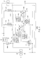
Figure 1 is a diagram showing an example of a circuit configuration of asystem 1000 including anLED driver circuit 100 according to a first embodiment; and -
Figure 2 is a diagram showing an example of a circuit configuration of asystem 1000a including a conventionalLED driver circuit 100a. - In the following, an embodiment of the present invention will be described with reference to the drawings.
- In a
system 1000 according to a first embodiment, anLED driver circuit 100 is configured to drive a first LED circuit "LC1" and a second LED circuit "LC2" that have one LED element or a plurality of LED elements connected in series with each other (Figure 1 ). - A positive electrode "BP" of the battery "B" is connected to a controlling part "X" via a main switch "MSW" and a battery terminal "TB". A negative electrode "BN" of the battery "B" is connected to the controlling part "X" via a ground terminal "TG". That is, the controlling part "X" is connected between the battery terminal "TB" and the ground terminal "TG" and is driven by an electric power supplied from the battery "B".
- The first LED circuit "LC1" has one LED element or a plurality of LED elements connected in series with each other and is connected to the positive electrode "BP" of the battery "B" at an anode side thereof.
- The second LED circuit "LC2" has one LED element or a plurality of LED elements connected in series with each other and is connected to the positive electrode "BP" of the battery "B" at an anode side thereof.
- The first LED circuit "LC1" and the second LED circuit "LC2" are LEDs of a headlamp of a motorcycle, for example. For example, the LED elements of the first LED circuit "LC1" are LED elements for a low beam, and the LED elements of the second LED circuit "LC2" are LED elements for a high beam.
- A first LED switch "LS1" capable of being turned on and off by a user is connected in series with the first LED circuit "LC1" between the positive electrode "BP" of the battery "B" and a first LED terminal "TL1".
- If the first LED switch "LS1" is turned on by the user, a current can flow to the first LED circuit "LC1". On the other hand, if the first LED switch "LS1" is turned off by the user, the current flowing to the first LED circuit "LC1" is interrupted.
- A second LED switch "LS2" capable of being turned on and off by the user is connected in series with the second LED circuit "LC2" between the positive electrode "BP" of the battery "B" and a second LED terminal "TL2".
- If the second LED switch "LS2" is turned on by the user, a current can flow to the second LED circuit "LC2". On the other hand, if the second LED switch "LS2" is turned off by the user, the current flowing to the second LED circuit "LC2" is interrupted.
- The first LED circuit "LC1", the second LED circuit "LC2", the first LED switch "LS1" and the second LED switch "LS2" form a headlamp unit 101 for a motorcycle.
- The main switch "MSW" is capable of being turned on and off by the user.
- A relay "RE" is connected between the positive electrode "BP" of the battery "B" and the anode sides of the first LED circuit "LC1" and the second LED circuit "LC2". More specifically, the relay "RE" is connected to the positive electrode "BP" of the battery at one end thereof and to the anode sides of the first LED circuit "LC1" and the second LED circuit "LC2" at another end thereof.
- If the main switch "MSW" is turned on, a current flows to a coil of the relay "RE" to turn on the relay "RE".
- A load "LO" is connected between the relay "RE" and the negative electrode "BN" of the battery "B". The load "LO" is an ignition device of an engine of a motorcycle, for example.
- As shown in
Figure 1 , theLED driver circuit 100 drives the first LED circuit "LC1" that has one LED element or a plurality of LED elements connected in series with each other and is connected to the positive electrode "BP" of the battery "B" at the anode side thereof, and the second LED circuit "LC2" that has one LED element or a plurality of LED elements connected in series with each other and is connected to the positive electrode "BP" of the battery "B" at the anode side thereof. - The
LED driver circuit 100 includes the first LED terminal "TL1", to which a cathode side of the first LED circuit "LC1" is connected, and the second LED terminal "TL2", to which a cathode side of the second LED circuit "LC2" is connected. - The
LED driver circuit 100 includes the ground terminal "TG" that is connected to the negative electrode "BN" of the battery "B", the battery terminal "TB" that is connected to the positive electrode "BP" of the battery "B" via the main switch "MSW", and a voltage detecting terminal "TD" that is connected to the positive electrode "BP" of the battery "B" via the relay "RE". - The
LED driver circuit 100 includes a first switch element "SW1" that is connected between the first LED terminal "TL1" and the ground terminal "TG", and a second switch element "SW2" that is connected between the second LED terminal "TL2" and the ground terminal "TG". - The
LED driver circuit 100 includes a first voltage detecting circuit "VD1" that detects a first terminal voltage at the first LED terminal "TL1", a second voltage detecting circuit "VD2" that detects a second terminal voltage at the second LED terminal "TL2", and a battery voltage detecting circuit "VDB" that detects a battery voltage of the battery "B". - The battery voltage detecting circuit "VDB" detects the battery voltage of the battery "B" by detecting the voltage at the voltage detecting terminal "TD", for example.
- As described above, the voltage detecting terminal "TD" is connected to the positive electrode "BP" of the battery "B" via the relay "RE". Therefore, when the relay "RE" is turned on, the battery voltage of the battery "B" is supplied to the voltage detecting terminal "TD". Therefore, the battery voltage detecting circuit "VDB" can detect the battery voltage of the battery "B" by detecting the voltage at the voltage detecting terminal "TD".
- The
LED driver circuit 100 includes the controlling part "X" that controls the first switch element "SW1" and the second switch element "SW2" in accordance with the first terminal voltage and the second terminal voltage. The controlling part "X" is connected between the battery terminal "TB" and the ground terminal "TG" and operates on the electric power that is supplied from the battery "B" when the main switch "MSW" is turned on. - As shown in
Figure 1 , the first switch element "SW1" is a first MOS transistor "M1" that is connected between the first LED terminal "TL1" and the ground terminal "TG" and whose gate voltage is controlled by the controlling part "X". As shown inFigure 1 , the second switch element "SW2" is a second MOS transistor "M2" that is connected between the second LED terminal "TL2" and the ground terminal "TG" and whose gate voltage is controlled by the controlling part "X". - The
LED driver circuit 100 includes a first reference voltage circuit "VR1" that outputs a first reference voltage controlled by the controlling part "X", and a first detecting resistor "R1" connected between the first switch element "SW1" and the ground terminal "TG". TheLED driver circuit 100 includes a first comparator "CON1" that compares the first reference voltage with a first detection voltage between the first switch element "SW1" and the first detecting resistor "R1" and outputs a first controlling signal that makes the first MOS transistor "M1" operate to make the first detection voltage and the first reference voltage equal to each other, and a first controlling resistor "Ra" connected between an output of the first comparator "CON1" and a gate of the first MOS transistor "M1". - The controlling part "X" controls the first reference voltage described above based on the first terminal voltage, thereby controlling the first controlling signal output from the first comparator "CON1" and supplied to the gate of the first MOS transistor "M1". In other words, the controlling part "X" controls the gate voltage of the first MOS transistor "M1" by controlling the first reference voltage.
- The
LED driver circuit 100 includes a second reference voltage circuit "VR2" that outputs a second reference voltage controlled by the controlling part "X", and a second detecting resistor "R2" connected between the second switch element "SW2" and the ground terminal "TG". TheLED driver circuit 100 includes a second comparator "CON2" that compares the second reference voltage with a second detection voltage between the second switch element "SW2" and the second detecting resistor "R2" and outputs a second controlling signal that makes the second MOS transistor "M2" operate to make the second detection voltage and the second reference voltage equal to each other, and a second controlling resistor "Rb" connected between an output of the second comparator "CON2" and a gate of the second MOS transistor "M2". - The controlling part "X" controls the second reference voltage described above based on the second terminal voltage, thereby controlling the second controlling signal output from the second comparator "CON2" and supplied to the gate of the second MOS transistor "M2". In other words, the controlling part "X" controls the gate voltage of the second MOS transistor "M2" by controlling the second reference voltage.
- If the first terminal voltage is lower than a preset first upper limit value, the controlling part "X" controls the first reference voltage to control the first switch element "SW1" with a first on-duty ratio with the first controlling signal. The first on-duty ratio is an on-duty ratio of 100%, for example.
- If the first terminal voltage reaches the first upper limit value, the controlling part "X" controls the first reference voltage to control the first switch element "SW1" with a second on-duty ratio smaller than the first on-duty ratio described above with the first controlling signal.
- If the second terminal voltage is lower than a preset second upper limit value, the controlling part "X" controls the second reference voltage to control the second switch element "SW2" with a third on-duty ratio with the second controlling signal. The third on-duty ratio is an on-duty ratio of 100%, for example.
- If the second terminal voltage reaches the second upper limit value, the controlling part "X" controls the second reference voltage to control the second switch element "SW2" with a fourth on-duty ratio smaller than the third on-duty ratio described above with the second controlling signal.
- Thus, the
LED driver circuit 100 requires no information on switching of the switches and therefore requires no external signal. In addition, theLED driver circuit 100 requires no constant-current power supply. - That is, the number of terminals, wires and the like of the
LED driver circuit 100 can be reduced. - Furthermore, when a battery abnormality or the like occurs and an overvoltage occurs, for example, the
LED driver circuit 100 can reduce heat generation of the MOS transistors and prevent the LED elements from suddenly going out, although the light intensity of the LED elements decreases. - If a first potential difference between the battery voltage and the first terminal voltage is equal to or lower than a first predefined value, the controlling part "X" controls the first reference voltage to lower the on-duty ratio of the first switch element "SW1".
- The first predefined value is set to be the potential difference between the first LED terminal "TL1" and the voltage detecting terminal "TD" at the time when the first LED switch "LS1" is in the on state and any of the LED elements of the first LED circuit "LC1" is short-circuited, for example.
- If a second potential difference between the battery voltage and the second terminal voltage is equal to or lower than a second predefined value, the controlling part "X" controls the second reference voltage to lower the on-duty ratio of the second switch element "SW2".
- The second predefined value is set to be the potential difference between the second LED terminal "TL2" and the voltage detecting terminal "TD" at the time when the second LED switch "LS2" is in the on state and any of the LED elements of the second LED circuit "LC2" is short-circuited, for example.
- In this way, when the potential difference between the battery voltage and the voltage at an LED terminal is equal to or lower than a predefined value (specifically, when at least any of the LED elements is short-circuited, for example), the on-duty ratio of the switch element (the MOS transistor) can be lowered to reduce heat generation of the switch element (the MOS transistor).
- In particular, the controlling part "X" may turn off the first switch element "SW1" when the first potential difference described above is equal to or lower than the third predefined value lower than the first predefined value.
- Similarly, the controlling part "X" may turn off the second switch element "SW2" when the second potential difference described above is equal to or lower than the fourth predefined value lower than the second predefined value.
- In this way, when the potential difference between the battery voltage and the voltage at an LED terminal is equal to or lower than a predefined value (specifically, when at least any of the LED elements is short-circuited, for example), the switch element (the MOS transistor) can be turned off to reduce heat generation of the switch element (the MOS transistor) with higher reliability.
- If a breakage occurs in an LED element of the first LED circuit "LC1", the connection between the positive electrode "BP" of the battery "B" and the first LED terminal "TL1" is interrupted. That is, the first terminal voltage at the first LED terminal "TL1" becomes equal to the voltage (the ground voltage) at the negative electrode "BN" of the battery "B".
- The controlling part "X" determines that a breakage has occurred in an LED element of the first LED circuit "LC1" if the first terminal voltage described above is equal to or lower than a preset first determination value. The first determination value is the ground voltage (the voltage at the negative electrode "BN" of the battery "B"), for example.
- Similarly, if a breakage occurs in an LED element of the second LED circuit "LC2", the connection between the positive electrode "BP" of the battery "B" and the second LED terminal "TL2" is interrupted. That is, the second terminal voltage at the second LED terminal "TL2" becomes equal to the voltage (the ground voltage) at the negative electrode "BN" of the battery "B".
- The controlling part "X" determines that a breakage has occurred in an LED element of the second LED circuit "LC2" if the second terminal voltage described above is equal to or lower than a preset second determination value. The second determination value is the ground voltage (the voltage at the negative electrode "BN" of the battery "B"), for example.
- In this way, the controlling part "X" can detect a breakage of the LED elements based on the first terminal voltage and the second terminal voltage. That is, the
LED driver circuit 100 can detect a breakage of any of the LED elements for the high beam and the low beam of the headlamp of the motorcycle, for example. - Next, an example of a method of controlling the
LED driver circuit 100 configured as described above will be described. - First, in response to the user turning on the main switch "MSW", for example, the controlling part "X" is made to operate (that is, activated) by an electric power supplied from the battery "B".
- Once the main switch "MSW" is turned on, the relay "RE" is turned on. As a result, an electric power can be supplied from the battery "B" to the headlamp unit 101. At this point in time, if the first and second LED switches "LS1", "LS2" are in the off state, no current flows to the first LED circuit "LC1" and the second LED circuit "LC2".
- The first terminal voltage then becomes equal to the ground voltage or, in other words, becomes lower than the first upper limit value. In addition, the second terminal voltage becomes equal to the ground voltage or, in other words, becomes lower than the second upper limit value.
- Since the first terminal voltage is lower than the preset first upper limit value, the controlling part "X" controls the first reference voltage to control the first switch element "SW1" with the first on-duty ratio (an on-duty ratio of 100%, for example) with the first controlling signal.
- Furthermore, since the second terminal voltage is lower than the preset second upper limit value, the controlling part "X" controls the second reference voltage to control the second switch element "SW2" with the third on-duty ratio (an on-duty ratio of 100%, for example) with the second controlling signal.
- Suppose that the user then turns on the first LED switch "LS1", for example. In that case, since the first switch element "SW1" is controlled with the first on-duty ratio, a predetermined amount of current flows to the first LED circuit "LC1", and the LED elements emit light.
- On the other hand, suppose that the user turns on the second LED switch "LS2". In that case, since the second switch element "SW2" is controlled with the third on-duty ratio, a predetermined amount of current flows to the second LED circuit "LC2", and the LED elements emit light.
- As can be seen from the above description, the
LED driver circuit 100 requires no information on switching of the switches and therefore requires no external signal. In addition, theLED driver circuit 100 requires no constant-current power supply. - After that, if a battery abnormality or the like occurs and an overvoltage occurs, for example, the first terminal voltage reaches the first upper limit value, and the second terminal voltage reaches the second upper limit value.
- Since the first terminal voltage has reached the first upper limit value, the controlling part "X" controls the first reference voltage to control the first switch element "SW1" with the second on-duty ratio smaller than the first on-duty ratio with the first controlling signal.
- As a result, the amount of current flowing to the first switch element "SW1" (the first MOS transistor "M1") is limited, and heat generation of the first switch element "SW1" is reduced.
- Furthermore, since the second terminal voltage has reached the second upper limit value, the controlling part "X" controls the second reference voltage to control the second switch element "SW2" with the fourth on-duty ratio smaller than the third on-duty ratio with the second controlling signal.
- As a result, the amount of current flowing to the second switch element "SW2" (the second MOS transistor "M2") is limited, and heat generation of the second switch element "SW2" is reduced.
- In this way, when a battery abnormality or the like occurs and an overvoltage occurs, the
LED driver circuit 100 can reduce heat generation of the switch elements (the MOS transistors) and prevent the LED elements from suddenly going out, although the light intensity of the LED elements decreases. - If any of the LED elements of the first LED circuit "LC1" is short-circuited, for example, the first potential difference between the battery voltage and the first terminal voltage becomes equal to or lower than the first predefined value. Since the first potential difference between the battery voltage and the first terminal voltage is equal to or lower than the first predefined value, the controlling part "X" controls the first reference voltage to lower the on-duty ratio of the first switch element "SW1".
- If any of the LED elements of the second LED circuit "LC2" is short-circuited, for example, the second potential difference between the battery voltage and the second terminal voltage becomes equal to or lower than the second predefined value. Since the second potential difference between the battery voltage and the second terminal voltage is equal to or lower than the second predefined value, the controlling part "X" controls the second reference voltage to lower the on-duty ratio of the second switch element "SW2".
- In this way, heat generation of the switch elements (the MOS transistors) can be reduced.
- The same operation is then repeated.
- As described above, the
LED driver circuit 100 according to an aspect of the present invention includes the first switch element "SW1" that is connected between the first LED terminal "TL1" and the ground terminal "TG", the second switch element "SW2" that is connected between the second LED terminal "TL2" and the ground terminal "TG", the first voltage detecting circuit "VD1" that detects the first terminal voltage at the first LED terminal "TL1", the second voltage detecting circuit "VD2" that detects the second terminal voltage at the second LED terminal "TL2", and the controlling part "X" that controls the first switch element "SW1" and the second switch element "SW2" based on the first terminal voltage and the second terminal voltage. - The first LED switch capable of being turned on and off by the user is connected in series with the first LED circuit "LC1" between the positive electrode "BP" of the battery and the first LED terminal "TL1".
- If the first terminal voltage is lower than the preset first upper limit value, the controlling part "X" controls the first switch element "SW1" with the first on-duty ratio. If the first terminal voltage reaches the first upper limit value, the controlling part "X" controls the first switch element "SW1" with the second on-duty ratio smaller than the first on-duty ratio. If the second terminal voltage is lower than the preset second upper limit value, the controlling part "X" controls the second switch element "SW2" with the third on-duty ratio. If the second terminal voltage reaches the second upper limit value, the controlling part "X" controls the second switch element "SW2" with the fourth on-duty ratio smaller than the third on-duty ratio.
- Thus, the
LED driver circuit 100 according to the present invention requires no information on switching of the switches and therefore requires no external signal. In addition, theLED driver circuit 100 requires no constant-current power supply. - That is, the number of terminals, wires and the like of the
LED driver circuit 100 can be reduced. - Furthermore, when a battery abnormality or the like occurs and an overvoltage occurs, the
LED driver circuit 100 according to the present invention can reduce heat generation of the MOS transistors and prevent the LED elements from suddenly going out, although the light intensity of the LED elements decreases. - If the first potential difference between the battery voltage and the first terminal voltage is equal to or lower than the first predefined value, the controlling part "X" lowers the on-duty ratio of the first switch element "SW1". If the second potential difference between the battery voltage and the second terminal voltage is equal to or lower than the second predefined value, the controlling part "X" lowers the on-duty ratio of the second switch element "SW2".
- In this way, when the potential difference between the battery voltage and the voltage at an LED terminal is equal to or lower than a predefined value (specifically, when at least any of the LED elements is short-circuited, for example), the on-duty ratio of the switch element (the MOS transistor) can be lowered to reduce heat generation of the switch element (the MOS transistor).
- Furthermore, if the first terminal voltage is equal to or lower than the preset first determination value, the controlling part "X" determines that a breakage has occurred in an LED element of the first LED circuit "LC1". If the second terminal voltage is equal to or lower than the preset second determination value, the controlling part "X" determines that a breakage has occurred in an LED element of the second LED circuit "LC2".
- Thus, if the voltage at an LED terminal for the low beam or high beam is zero (equal to or lower than the determination value), it can be determined that a breakage has occurred in the LED element for the low beam or high beam.
- As described above, the
LED driver circuit 100 can detect a breakage of any of the LED elements for the high beam and the low beam of a headlamp of a motorcycle, for example. - Although an embodiment of the present invention has been described, the embodiment is shown for illustrative purposes and is not intended to limit the scope of the present invention. Various other embodiments are also possible, and various omissions, replacements and modifications can be made to the embodiment without departing from the spirit of the present invention. The embodiment and variations thereof are included in the scope and spirit of the present invention and included in the scope of the present invention described in the claims and equivalents thereof.
Claims (10)
- An LED driver circuit that drives a first LED circuit and a second LED circuit, the first LED circuit having one LED element or a plurality of LED elements connected in series with each other and being connected to a positive electrode of a battery at an anode side thereof, and the second LED circuit having one LED element or a plurality of LED elements connected in series with each other and being connected to the positive electrode of the battery at an anode side thereof, the LED driver circuit comprising:a first LED terminal to which a cathode side of the first LED circuit is connected;a second LED terminal to which a cathode side of the second LED circuit is connected;a ground terminal connected to a negative electrode of the battery;a first switch element connected between the first LED terminal and the ground terminal;a second switch element connected between the second LED terminal and the ground terminal;a first voltage detecting circuit that detects a first terminal voltage at the first LED terminal;a second voltage detecting circuit that detects a second terminal voltage at the second LED terminal; anda controlling part that controls the first switch element and the second switch element in accordance with the first terminal voltage and the second terminal voltage,wherein a first LED switch capable of being turned on and off by a user is connected in series with the first LED circuit between the positive electrode of the battery and the first LED terminal, andthe controlling partcontrols the first switch element with a first on-duty ratio if the first terminal voltage is lower than a preset first upper limit value,controls the first switch element with a second on-duty ratio smaller than the first on-duty ratio if the first terminal voltage reaches the first upper limit value,controls the second switch element with a third on-duty ratio if the second terminal voltage is lower than a preset second upper limit value, andcontrols the second switch element with a fourth on-duty ratio smaller than the third on-duty ratio if the second terminal voltage reaches the second upper limit value.
- The LED driver circuit according to claim 1, further comprising:a battery voltage detecting circuit that detects a battery voltage of the battery,wherein the controlling partlowers the on-duty ratio of the first switch element if a first potential difference between the battery voltage and the first terminal voltage is equal to or lower than a first predefined value, andlowers the on-duty ratio of the second switch element if a second potential difference between the battery voltage and the second terminal voltage is equal to or lower than a second predefined value.
- The LED driver circuit according to claim 2, wherein the controlling part
turns off the first switch element if the first potential difference is equal to or lower than a third predefined value lower than the first predefined value, and
turns off the second switch element if the second potential difference is equal to or lower than a fourth predefined value lower than the second predefined value. - The LED driver circuit according to claim 1, wherein the controlling part
determines that a breakage has occurred in an LED element of the first LED circuit if the first terminal voltage is equal to or lower than a preset first determination value, and
determines that a breakage has occurred in an LED element of the second LED circuit if the second terminal voltage is equal to or lower than a preset second determination value. - The LED driver circuit according to claim 4, wherein the first determination value and the second determination value are the ground voltage.
- The LED driver circuit according to claim 1, wherein the first on-duty ratio and the third on-duty ratio are an on-duty ratio of 100%.
- The LED driver circuit according to claim 1, wherein a second LED switch capable of being turned on and off by a user is connected in series with the second LED circuit between the positive electrode of the battery and the second LED terminal.
- The LED driver circuit according to claim 1, wherein a first end of a relay is connected to the positive electrode of the battery, and a second end of the relay is connected to the anode side of the first LED circuit and the anode side of the second LED circuit,
a load is connected between the second end of the relay and the negative electrode of the battery,
the first LED circuit and the second LED circuit are LEDs of a headlamp of a motorcycle, and
the load is an ignition device of an engine of the motorcycle. - The LED driver circuit according to claim 1, wherein the first switch element is a first MOS transistor that is connected between the first LED terminal and the ground terminal and whose gate voltage is controlled by the controlling part,
the second switch element is a second MOS transistor that is connected between the second LED terminal and the ground terminal and whose gate voltage is controlled by the controlling part,
the LED driver circuit further comprises:a first reference voltage circuit that outputs a first reference voltage controlled by the controlling part;a first detecting resistor connected between the first switch element and the ground terminal;a first comparator that compares the first reference voltage with a first detection voltage between the first switch element and the first detecting resistor and outputs a first controlling signal that makes the first MOS transistor operate to make the first reference voltage and the first detection voltage equal to each other;a first controlling resistor connected between an output of the first comparator and a gate of the first MOS transistor;a second reference voltage circuit that outputs a second reference voltage controlled by the controlling part;a second detecting resistor connected between the second switch element and the ground terminal;a second comparator that compares the second reference voltage with a second detection voltage between the second switch element and the second detecting resistor and outputs a second controlling signal that makes the second MOS transistor operate to make the second reference voltage and the second detection voltage equal to each other; anda second controlling resistor connected between an output of the second comparator and a gate of the second MOS transistor, andthe controlling part
controls the first reference voltage to make the first switch element operate with the first on-duty ratio with the first controlling signal if the first terminal voltage is lower than the first upper limit value,
controls the first reference voltage to make the first switch element operate with the second on-duty ratio with the first controlling signal if the first terminal voltage reaches the first upper limit value,
controls the second reference voltage to make the second switch element operate with the third on-duty ratio with the second controlling signal if the second terminal voltage is lower than the second upper limit value, and
controls the second reference voltage to make the second switch element operate with the fourth on-duty ratio with the second controlling signal if the second terminal voltage reaches the second upper limit value. - A method of controlling an LED driver circuit, the LED driver circuit that drives a first LED circuit and a second LED circuit, the first LED circuit having one LED element or a plurality of LED elements connected in series with each other and being connected to a positive electrode of a battery at an anode side thereof, the second LED circuit having one LED element or a plurality of LED elements connected in series with each other and being connected to the positive electrode of the battery at an anode side thereof, and the LED driver circuit comprising a first LED terminal to which a cathode side of the first LED circuit is connected, a second LED terminal to which a cathode side of the second LED circuit is connected, a ground terminal connected to a negative electrode of the battery, a first switch element connected between the first LED terminal and the ground terminal, a second switch element connected between the second LED terminal and the ground terminal, a first voltage detecting circuit that detects a first terminal voltage at the first LED terminal, a second voltage detecting circuit that detects a second terminal voltage at the second LED terminal, and a controlling part that controls the first switch element and the second switch element in accordance with the first terminal voltage and the second terminal voltage,
wherein a first LED switch capable of being turned on and off by a user is connected in series with the first LED circuit between the positive electrode of the battery and the first LED terminal, and
the controlling part
controls the first switch element with a first on-duty ratio if the first terminal voltage is lower than a preset first upper limit value,
controls the first switch element with a second on-duty ratio smaller than the first on-duty ratio if the first terminal voltage reaches the first upper limit value,
controls the second switch element with a third on-duty ratio if the second terminal voltage is lower than a preset second upper limit value, and
controls the second switch element with a fourth on-duty ratio smaller than the third on-duty ratio if the second terminal voltage reaches the second upper limit value.
Applications Claiming Priority (1)
| Application Number | Priority Date | Filing Date | Title |
|---|---|---|---|
| PCT/JP2013/083706 WO2015092864A1 (en) | 2013-12-17 | 2013-12-17 | Led driver circuit and method for controlling led driver circuit |
Publications (3)
| Publication Number | Publication Date |
|---|---|
| EP3086377A1 true EP3086377A1 (en) | 2016-10-26 |
| EP3086377A4 EP3086377A4 (en) | 2017-08-02 |
| EP3086377B1 EP3086377B1 (en) | 2019-08-14 |
Family
ID=53402260
Family Applications (1)
| Application Number | Title | Priority Date | Filing Date |
|---|---|---|---|
| EP13899599.8A Active EP3086377B1 (en) | 2013-12-17 | 2013-12-17 | Led driver circuit and method of controlling led driver circuit |
Country Status (3)
| Country | Link |
|---|---|
| EP (1) | EP3086377B1 (en) |
| JP (1) | JP5897768B2 (en) |
| WO (1) | WO2015092864A1 (en) |
Cited By (1)
| Publication number | Priority date | Publication date | Assignee | Title |
|---|---|---|---|---|
| EP3255959A1 (en) * | 2016-06-07 | 2017-12-13 | ZKW Group GmbH | Motor vehicle lighting device |
Families Citing this family (1)
| Publication number | Priority date | Publication date | Assignee | Title |
|---|---|---|---|---|
| WO2019009232A1 (en) | 2017-07-04 | 2019-01-10 | ローム株式会社 | Load drive device |
Family Cites Families (5)
| Publication number | Priority date | Publication date | Assignee | Title |
|---|---|---|---|---|
| JP2008218457A (en) | 2007-02-28 | 2008-09-18 | Stanley Electric Co Ltd | Light control circuit for LED vehicle lamp |
| JP4918929B2 (en) * | 2009-01-30 | 2012-04-18 | 日本テキサス・インスツルメンツ株式会社 | Light-emitting diode controller |
| JP2010277226A (en) | 2009-05-27 | 2010-12-09 | Sharp Corp | DC stabilized power supply device and electronic device including the same |
| DE102011003519A1 (en) * | 2011-02-02 | 2012-08-02 | Robert Bosch Gmbh | Method for controlling flow of current through LED-strands for background lighting of thin film transistor-LED in motor vehicle, involves determining reference value for control loop for controlling flow of current through elements |
| JP2013021117A (en) * | 2011-07-11 | 2013-01-31 | Rohm Co Ltd | Led drive device, luminaire, and liquid crystal display device |
-
2013
- 2013-12-17 WO PCT/JP2013/083706 patent/WO2015092864A1/en not_active Ceased
- 2013-12-17 EP EP13899599.8A patent/EP3086377B1/en active Active
- 2013-12-17 JP JP2015511849A patent/JP5897768B2/en active Active
Cited By (1)
| Publication number | Priority date | Publication date | Assignee | Title |
|---|---|---|---|---|
| EP3255959A1 (en) * | 2016-06-07 | 2017-12-13 | ZKW Group GmbH | Motor vehicle lighting device |
Also Published As
| Publication number | Publication date |
|---|---|
| EP3086377A4 (en) | 2017-08-02 |
| WO2015092864A1 (en) | 2015-06-25 |
| JP5897768B2 (en) | 2016-03-30 |
| JPWO2015092864A1 (en) | 2017-03-16 |
| EP3086377B1 (en) | 2019-08-14 |
Similar Documents
| Publication | Publication Date | Title |
|---|---|---|
| JP4400880B2 (en) | Lighting control circuit for vehicular lamp | |
| JP4714701B2 (en) | LED vehicle lighting control circuit | |
| US9162607B2 (en) | Vehicular lamp | |
| JP6302748B2 (en) | LED lamp, LED lighting device, and LED lighting system using the same | |
| JP5301976B2 (en) | Control device for vehicular lamp | |
| EP3261413B1 (en) | Power supply circuit for led lighting | |
| JP6775189B2 (en) | Lighting device and vehicle | |
| US8330375B2 (en) | Vehicle lamp lighting control device | |
| JP2006210219A (en) | Lighting control circuit for vehicular lamp | |
| JP2006103404A (en) | Lighting control circuit for vehicular lamp | |
| US9345075B2 (en) | Vehicular headlamp | |
| JP2014170880A (en) | Light-emitting element switch-on device and light source device | |
| JP6302706B2 (en) | VEHICLE LIGHT AND DRIVE DEVICE THEREOF | |
| US9107271B2 (en) | LED driving circuit | |
| US8324839B2 (en) | Lamp control system | |
| EP3086377B1 (en) | Led driver circuit and method of controlling led driver circuit | |
| WO2014171015A1 (en) | Lamp drive power supply and method for controlling lamp drive power supply | |
| CN111225478A (en) | Switch module protection circuit | |
| JP7340383B2 (en) | dimmer circuit | |
| JP5187756B2 (en) | Light emitting device for vehicle lamp | |
| US10869375B2 (en) | Vehicle lighting device | |
| KR20160110799A (en) | Circuit and method for detecting short circuit in LED lamp | |
| JP7163486B2 (en) | load driver | |
| WO2015092863A1 (en) | Led driver circuit and method for controlling led driver circuit | |
| JP6558062B2 (en) | LED module |
Legal Events
| Date | Code | Title | Description |
|---|---|---|---|
| PUAI | Public reference made under article 153(3) epc to a published international application that has entered the european phase |
Free format text: ORIGINAL CODE: 0009012 |
|
| 17P | Request for examination filed |
Effective date: 20150713 |
|
| AK | Designated contracting states |
Kind code of ref document: A1 Designated state(s): AL AT BE BG CH CY CZ DE DK EE ES FI FR GB GR HR HU IE IS IT LI LT LU LV MC MK MT NL NO PL PT RO RS SE SI SK SM TR |
|
| AX | Request for extension of the european patent |
Extension state: BA ME |
|
| DAX | Request for extension of the european patent (deleted) | ||
| REG | Reference to a national code |
Ref country code: DE Ref legal event code: R079 Ref document number: 602013059339 Country of ref document: DE Free format text: PREVIOUS MAIN CLASS: H01L0033000000 Ipc: H05B0033080000 |
|
| A4 | Supplementary search report drawn up and despatched |
Effective date: 20170629 |
|
| RIC1 | Information provided on ipc code assigned before grant |
Ipc: H05B 33/08 20060101AFI20170623BHEP |
|
| GRAP | Despatch of communication of intention to grant a patent |
Free format text: ORIGINAL CODE: EPIDOSNIGR1 |
|
| STAA | Information on the status of an ep patent application or granted ep patent |
Free format text: STATUS: GRANT OF PATENT IS INTENDED |
|
| INTG | Intention to grant announced |
Effective date: 20190409 |
|
| RIN1 | Information on inventor provided before grant (corrected) |
Inventor name: KOBAYASHI, KEISUKE Inventor name: OKAMOTO, AKIHIRO |
|
| GRAS | Grant fee paid |
Free format text: ORIGINAL CODE: EPIDOSNIGR3 |
|
| GRAA | (expected) grant |
Free format text: ORIGINAL CODE: 0009210 |
|
| STAA | Information on the status of an ep patent application or granted ep patent |
Free format text: STATUS: THE PATENT HAS BEEN GRANTED |
|
| AK | Designated contracting states |
Kind code of ref document: B1 Designated state(s): AL AT BE BG CH CY CZ DE DK EE ES FI FR GB GR HR HU IE IS IT LI LT LU LV MC MK MT NL NO PL PT RO RS SE SI SK SM TR |
|
| REG | Reference to a national code |
Ref country code: GB Ref legal event code: FG4D |
|
| REG | Reference to a national code |
Ref country code: CH Ref legal event code: EP Ref country code: AT Ref legal event code: REF Ref document number: 1168581 Country of ref document: AT Kind code of ref document: T Effective date: 20190815 |
|
| REG | Reference to a national code |
Ref country code: IE Ref legal event code: FG4D |
|
| REG | Reference to a national code |
Ref country code: DE Ref legal event code: R096 Ref document number: 602013059339 Country of ref document: DE |
|
| REG | Reference to a national code |
Ref country code: DE Ref legal event code: R079 Ref document number: 602013059339 Country of ref document: DE Free format text: PREVIOUS MAIN CLASS: H05B0033080000 Ipc: H05B0045000000 |
|
| REG | Reference to a national code |
Ref country code: NL Ref legal event code: MP Effective date: 20190814 |
|
| REG | Reference to a national code |
Ref country code: LT Ref legal event code: MG4D |
|
| PG25 | Lapsed in a contracting state [announced via postgrant information from national office to epo] |
Ref country code: NO Free format text: LAPSE BECAUSE OF FAILURE TO SUBMIT A TRANSLATION OF THE DESCRIPTION OR TO PAY THE FEE WITHIN THE PRESCRIBED TIME-LIMIT Effective date: 20191114 Ref country code: BG Free format text: LAPSE BECAUSE OF FAILURE TO SUBMIT A TRANSLATION OF THE DESCRIPTION OR TO PAY THE FEE WITHIN THE PRESCRIBED TIME-LIMIT Effective date: 20191114 Ref country code: SE Free format text: LAPSE BECAUSE OF FAILURE TO SUBMIT A TRANSLATION OF THE DESCRIPTION OR TO PAY THE FEE WITHIN THE PRESCRIBED TIME-LIMIT Effective date: 20190814 Ref country code: NL Free format text: LAPSE BECAUSE OF FAILURE TO SUBMIT A TRANSLATION OF THE DESCRIPTION OR TO PAY THE FEE WITHIN THE PRESCRIBED TIME-LIMIT Effective date: 20190814 Ref country code: FI Free format text: LAPSE BECAUSE OF FAILURE TO SUBMIT A TRANSLATION OF THE DESCRIPTION OR TO PAY THE FEE WITHIN THE PRESCRIBED TIME-LIMIT Effective date: 20190814 Ref country code: LT Free format text: LAPSE BECAUSE OF FAILURE TO SUBMIT A TRANSLATION OF THE DESCRIPTION OR TO PAY THE FEE WITHIN THE PRESCRIBED TIME-LIMIT Effective date: 20190814 Ref country code: PT Free format text: LAPSE BECAUSE OF FAILURE TO SUBMIT A TRANSLATION OF THE DESCRIPTION OR TO PAY THE FEE WITHIN THE PRESCRIBED TIME-LIMIT Effective date: 20191216 Ref country code: HR Free format text: LAPSE BECAUSE OF FAILURE TO SUBMIT A TRANSLATION OF THE DESCRIPTION OR TO PAY THE FEE WITHIN THE PRESCRIBED TIME-LIMIT Effective date: 20190814 |
|
| REG | Reference to a national code |
Ref country code: AT Ref legal event code: MK05 Ref document number: 1168581 Country of ref document: AT Kind code of ref document: T Effective date: 20190814 |
|
| PG25 | Lapsed in a contracting state [announced via postgrant information from national office to epo] |
Ref country code: GR Free format text: LAPSE BECAUSE OF FAILURE TO SUBMIT A TRANSLATION OF THE DESCRIPTION OR TO PAY THE FEE WITHIN THE PRESCRIBED TIME-LIMIT Effective date: 20191115 Ref country code: LV Free format text: LAPSE BECAUSE OF FAILURE TO SUBMIT A TRANSLATION OF THE DESCRIPTION OR TO PAY THE FEE WITHIN THE PRESCRIBED TIME-LIMIT Effective date: 20190814 Ref country code: AL Free format text: LAPSE BECAUSE OF FAILURE TO SUBMIT A TRANSLATION OF THE DESCRIPTION OR TO PAY THE FEE WITHIN THE PRESCRIBED TIME-LIMIT Effective date: 20190814 Ref country code: IS Free format text: LAPSE BECAUSE OF FAILURE TO SUBMIT A TRANSLATION OF THE DESCRIPTION OR TO PAY THE FEE WITHIN THE PRESCRIBED TIME-LIMIT Effective date: 20191214 Ref country code: RS Free format text: LAPSE BECAUSE OF FAILURE TO SUBMIT A TRANSLATION OF THE DESCRIPTION OR TO PAY THE FEE WITHIN THE PRESCRIBED TIME-LIMIT Effective date: 20190814 Ref country code: ES Free format text: LAPSE BECAUSE OF FAILURE TO SUBMIT A TRANSLATION OF THE DESCRIPTION OR TO PAY THE FEE WITHIN THE PRESCRIBED TIME-LIMIT Effective date: 20190814 |
|
| PG25 | Lapsed in a contracting state [announced via postgrant information from national office to epo] |
Ref country code: TR Free format text: LAPSE BECAUSE OF FAILURE TO SUBMIT A TRANSLATION OF THE DESCRIPTION OR TO PAY THE FEE WITHIN THE PRESCRIBED TIME-LIMIT Effective date: 20190814 |
|
| PG25 | Lapsed in a contracting state [announced via postgrant information from national office to epo] |
Ref country code: DK Free format text: LAPSE BECAUSE OF FAILURE TO SUBMIT A TRANSLATION OF THE DESCRIPTION OR TO PAY THE FEE WITHIN THE PRESCRIBED TIME-LIMIT Effective date: 20190814 Ref country code: EE Free format text: LAPSE BECAUSE OF FAILURE TO SUBMIT A TRANSLATION OF THE DESCRIPTION OR TO PAY THE FEE WITHIN THE PRESCRIBED TIME-LIMIT Effective date: 20190814 Ref country code: PL Free format text: LAPSE BECAUSE OF FAILURE TO SUBMIT A TRANSLATION OF THE DESCRIPTION OR TO PAY THE FEE WITHIN THE PRESCRIBED TIME-LIMIT Effective date: 20190814 Ref country code: AT Free format text: LAPSE BECAUSE OF FAILURE TO SUBMIT A TRANSLATION OF THE DESCRIPTION OR TO PAY THE FEE WITHIN THE PRESCRIBED TIME-LIMIT Effective date: 20190814 Ref country code: RO Free format text: LAPSE BECAUSE OF FAILURE TO SUBMIT A TRANSLATION OF THE DESCRIPTION OR TO PAY THE FEE WITHIN THE PRESCRIBED TIME-LIMIT Effective date: 20190814 |
|
| PG25 | Lapsed in a contracting state [announced via postgrant information from national office to epo] |
Ref country code: CZ Free format text: LAPSE BECAUSE OF FAILURE TO SUBMIT A TRANSLATION OF THE DESCRIPTION OR TO PAY THE FEE WITHIN THE PRESCRIBED TIME-LIMIT Effective date: 20190814 Ref country code: SK Free format text: LAPSE BECAUSE OF FAILURE TO SUBMIT A TRANSLATION OF THE DESCRIPTION OR TO PAY THE FEE WITHIN THE PRESCRIBED TIME-LIMIT Effective date: 20190814 Ref country code: SM Free format text: LAPSE BECAUSE OF FAILURE TO SUBMIT A TRANSLATION OF THE DESCRIPTION OR TO PAY THE FEE WITHIN THE PRESCRIBED TIME-LIMIT Effective date: 20190814 Ref country code: IS Free format text: LAPSE BECAUSE OF FAILURE TO SUBMIT A TRANSLATION OF THE DESCRIPTION OR TO PAY THE FEE WITHIN THE PRESCRIBED TIME-LIMIT Effective date: 20200224 |
|
| REG | Reference to a national code |
Ref country code: DE Ref legal event code: R097 Ref document number: 602013059339 Country of ref document: DE |
|
| REG | Reference to a national code |
Ref country code: DE Ref legal event code: R119 Ref document number: 602013059339 Country of ref document: DE |
|
| PLBE | No opposition filed within time limit |
Free format text: ORIGINAL CODE: 0009261 |
|
| STAA | Information on the status of an ep patent application or granted ep patent |
Free format text: STATUS: NO OPPOSITION FILED WITHIN TIME LIMIT |
|
| PG2D | Information on lapse in contracting state deleted |
Ref country code: IS |
|
| REG | Reference to a national code |
Ref country code: CH Ref legal event code: PL |
|
| 26N | No opposition filed |
Effective date: 20200603 |
|
| REG | Reference to a national code |
Ref country code: BE Ref legal event code: MM Effective date: 20191231 |
|
| PG25 | Lapsed in a contracting state [announced via postgrant information from national office to epo] |
Ref country code: SI Free format text: LAPSE BECAUSE OF FAILURE TO SUBMIT A TRANSLATION OF THE DESCRIPTION OR TO PAY THE FEE WITHIN THE PRESCRIBED TIME-LIMIT Effective date: 20190814 Ref country code: MC Free format text: LAPSE BECAUSE OF FAILURE TO SUBMIT A TRANSLATION OF THE DESCRIPTION OR TO PAY THE FEE WITHIN THE PRESCRIBED TIME-LIMIT Effective date: 20190814 |
|
| GBPC | Gb: european patent ceased through non-payment of renewal fee |
Effective date: 20191217 |
|
| PG25 | Lapsed in a contracting state [announced via postgrant information from national office to epo] |
Ref country code: IE Free format text: LAPSE BECAUSE OF NON-PAYMENT OF DUE FEES Effective date: 20191217 Ref country code: LU Free format text: LAPSE BECAUSE OF NON-PAYMENT OF DUE FEES Effective date: 20191217 Ref country code: DE Free format text: LAPSE BECAUSE OF NON-PAYMENT OF DUE FEES Effective date: 20200701 Ref country code: FR Free format text: LAPSE BECAUSE OF NON-PAYMENT OF DUE FEES Effective date: 20191231 Ref country code: GB Free format text: LAPSE BECAUSE OF NON-PAYMENT OF DUE FEES Effective date: 20191217 |
|
| PG25 | Lapsed in a contracting state [announced via postgrant information from national office to epo] |
Ref country code: BE Free format text: LAPSE BECAUSE OF NON-PAYMENT OF DUE FEES Effective date: 20191231 Ref country code: CH Free format text: LAPSE BECAUSE OF NON-PAYMENT OF DUE FEES Effective date: 20191231 Ref country code: LI Free format text: LAPSE BECAUSE OF NON-PAYMENT OF DUE FEES Effective date: 20191231 |
|
| PG25 | Lapsed in a contracting state [announced via postgrant information from national office to epo] |
Ref country code: CY Free format text: LAPSE BECAUSE OF FAILURE TO SUBMIT A TRANSLATION OF THE DESCRIPTION OR TO PAY THE FEE WITHIN THE PRESCRIBED TIME-LIMIT Effective date: 20190814 |
|
| PG25 | Lapsed in a contracting state [announced via postgrant information from national office to epo] |
Ref country code: MT Free format text: LAPSE BECAUSE OF FAILURE TO SUBMIT A TRANSLATION OF THE DESCRIPTION OR TO PAY THE FEE WITHIN THE PRESCRIBED TIME-LIMIT Effective date: 20190814 Ref country code: HU Free format text: LAPSE BECAUSE OF FAILURE TO SUBMIT A TRANSLATION OF THE DESCRIPTION OR TO PAY THE FEE WITHIN THE PRESCRIBED TIME-LIMIT; INVALID AB INITIO Effective date: 20131217 |
|
| PG25 | Lapsed in a contracting state [announced via postgrant information from national office to epo] |
Ref country code: MK Free format text: LAPSE BECAUSE OF FAILURE TO SUBMIT A TRANSLATION OF THE DESCRIPTION OR TO PAY THE FEE WITHIN THE PRESCRIBED TIME-LIMIT Effective date: 20190814 |
|
| PGFP | Annual fee paid to national office [announced via postgrant information from national office to epo] |
Ref country code: IT Payment date: 20251223 Year of fee payment: 13 |