EP3079158A1 - High-frequency electrical wire and coil - Google Patents
High-frequency electrical wire and coil Download PDFInfo
- Publication number
- EP3079158A1 EP3079158A1 EP14867830.3A EP14867830A EP3079158A1 EP 3079158 A1 EP3079158 A1 EP 3079158A1 EP 14867830 A EP14867830 A EP 14867830A EP 3079158 A1 EP3079158 A1 EP 3079158A1
- Authority
- EP
- European Patent Office
- Prior art keywords
- copper
- wire
- frequency
- coating
- outer layer
- Prior art date
- Legal status (The legal status is an assumption and is not a legal conclusion. Google has not performed a legal analysis and makes no representation as to the accuracy of the status listed.)
- Withdrawn
Links
- RYGMFSIKBFXOCR-UHFFFAOYSA-N Copper Chemical compound [Cu] RYGMFSIKBFXOCR-UHFFFAOYSA-N 0.000 claims abstract description 223
- 239000010949 copper Substances 0.000 claims abstract description 90
- 239000004020 conductor Substances 0.000 claims abstract description 83
- 229910052802 copper Inorganic materials 0.000 claims abstract description 76
- 239000000463 material Substances 0.000 claims abstract description 39
- 230000035699 permeability Effects 0.000 claims abstract description 17
- 239000010410 layer Substances 0.000 claims description 176
- 239000011248 coating agent Substances 0.000 claims description 82
- 238000000576 coating method Methods 0.000 claims description 82
- 238000009413 insulation Methods 0.000 claims description 13
- 239000011247 coating layer Substances 0.000 claims description 9
- 230000000052 comparative effect Effects 0.000 description 60
- 229910001120 nichrome Inorganic materials 0.000 description 40
- 239000004411 aluminium Substances 0.000 description 36
- 229910052782 aluminium Inorganic materials 0.000 description 36
- XAGFODPZIPBFFR-UHFFFAOYSA-N aluminium Chemical compound [Al] XAGFODPZIPBFFR-UHFFFAOYSA-N 0.000 description 36
- 238000004364 calculation method Methods 0.000 description 36
- 238000010586 diagram Methods 0.000 description 36
- 229910000831 Steel Inorganic materials 0.000 description 33
- 239000010959 steel Substances 0.000 description 33
- 230000000694 effects Effects 0.000 description 30
- 238000009826 distribution Methods 0.000 description 19
- WABPQHHGFIMREM-UHFFFAOYSA-N lead(0) Chemical compound [Pb] WABPQHHGFIMREM-UHFFFAOYSA-N 0.000 description 17
- 238000000611 regression analysis Methods 0.000 description 13
- PXHVJJICTQNCMI-UHFFFAOYSA-N Nickel Chemical compound [Ni] PXHVJJICTQNCMI-UHFFFAOYSA-N 0.000 description 11
- 230000002500 effect on skin Effects 0.000 description 11
- 230000008901 benefit Effects 0.000 description 9
- 229910045601 alloy Inorganic materials 0.000 description 8
- 239000000956 alloy Substances 0.000 description 8
- XEEYBQQBJWHFJM-UHFFFAOYSA-N Iron Chemical compound [Fe] XEEYBQQBJWHFJM-UHFFFAOYSA-N 0.000 description 7
- 230000009467 reduction Effects 0.000 description 7
- 230000005611 electricity Effects 0.000 description 6
- 238000004519 manufacturing process Methods 0.000 description 6
- 238000004458 analytical method Methods 0.000 description 5
- 238000000034 method Methods 0.000 description 5
- 229910052759 nickel Inorganic materials 0.000 description 5
- 238000010992 reflux Methods 0.000 description 5
- 229910000838 Al alloy Inorganic materials 0.000 description 4
- 238000012886 linear function Methods 0.000 description 4
- 238000004804 winding Methods 0.000 description 4
- 238000005491 wire drawing Methods 0.000 description 4
- 229910052742 iron Inorganic materials 0.000 description 3
- 229910052751 metal Inorganic materials 0.000 description 3
- 239000002184 metal Substances 0.000 description 3
- 238000004088 simulation Methods 0.000 description 3
- 239000002356 single layer Substances 0.000 description 3
- 229910000906 Bronze Inorganic materials 0.000 description 2
- 229910000640 Fe alloy Inorganic materials 0.000 description 2
- 229910000990 Ni alloy Inorganic materials 0.000 description 2
- XUIMIQQOPSSXEZ-UHFFFAOYSA-N Silicon Chemical compound [Si] XUIMIQQOPSSXEZ-UHFFFAOYSA-N 0.000 description 2
- 239000010974 bronze Substances 0.000 description 2
- KUNSUQLRTQLHQQ-UHFFFAOYSA-N copper tin Chemical compound [Cu].[Sn] KUNSUQLRTQLHQQ-UHFFFAOYSA-N 0.000 description 2
- 230000005684 electric field Effects 0.000 description 2
- 239000002320 enamel (paints) Substances 0.000 description 2
- 238000010438 heat treatment Methods 0.000 description 2
- 230000006698 induction Effects 0.000 description 2
- 239000000696 magnetic material Substances 0.000 description 2
- NRNCYVBFPDDJNE-UHFFFAOYSA-N pemoline Chemical compound O1C(N)=NC(=O)C1C1=CC=CC=C1 NRNCYVBFPDDJNE-UHFFFAOYSA-N 0.000 description 2
- 229910052710 silicon Inorganic materials 0.000 description 2
- 239000010703 silicon Substances 0.000 description 2
- 229910052709 silver Inorganic materials 0.000 description 2
- 239000004332 silver Substances 0.000 description 2
- 239000000126 substance Substances 0.000 description 2
- WFKWXMTUELFFGS-UHFFFAOYSA-N tungsten Chemical compound [W] WFKWXMTUELFFGS-UHFFFAOYSA-N 0.000 description 2
- 229910052721 tungsten Inorganic materials 0.000 description 2
- 239000010937 tungsten Substances 0.000 description 2
- 238000003466 welding Methods 0.000 description 2
- 229910018464 Al—Mg—Si Inorganic materials 0.000 description 1
- 229910000952 Be alloy Inorganic materials 0.000 description 1
- 229910001369 Brass Inorganic materials 0.000 description 1
- OKTJSMMVPCPJKN-UHFFFAOYSA-N Carbon Chemical compound [C] OKTJSMMVPCPJKN-UHFFFAOYSA-N 0.000 description 1
- VYZAMTAEIAYCRO-UHFFFAOYSA-N Chromium Chemical compound [Cr] VYZAMTAEIAYCRO-UHFFFAOYSA-N 0.000 description 1
- 229910000881 Cu alloy Inorganic materials 0.000 description 1
- VGGSQFUCUMXWEO-UHFFFAOYSA-N Ethene Chemical compound C=C VGGSQFUCUMXWEO-UHFFFAOYSA-N 0.000 description 1
- 239000005977 Ethylene Substances 0.000 description 1
- FYYHWMGAXLPEAU-UHFFFAOYSA-N Magnesium Chemical compound [Mg] FYYHWMGAXLPEAU-UHFFFAOYSA-N 0.000 description 1
- 241001676573 Minium Species 0.000 description 1
- OAICVXFJPJFONN-UHFFFAOYSA-N Phosphorus Chemical compound [P] OAICVXFJPJFONN-UHFFFAOYSA-N 0.000 description 1
- 239000004962 Polyamide-imide Substances 0.000 description 1
- 239000004698 Polyethylene Substances 0.000 description 1
- 239000004642 Polyimide Substances 0.000 description 1
- 229910000676 Si alloy Inorganic materials 0.000 description 1
- RTAQQCXQSZGOHL-UHFFFAOYSA-N Titanium Chemical compound [Ti] RTAQQCXQSZGOHL-UHFFFAOYSA-N 0.000 description 1
- 230000015572 biosynthetic process Effects 0.000 description 1
- 239000010951 brass Substances 0.000 description 1
- 229910052799 carbon Inorganic materials 0.000 description 1
- 229910052804 chromium Inorganic materials 0.000 description 1
- 239000011651 chromium Substances 0.000 description 1
- 239000002131 composite material Substances 0.000 description 1
- 238000010411 cooking Methods 0.000 description 1
- 210000003298 dental enamel Anatomy 0.000 description 1
- 238000006073 displacement reaction Methods 0.000 description 1
- 229920001971 elastomer Polymers 0.000 description 1
- 230000020169 heat generation Effects 0.000 description 1
- 239000011777 magnesium Substances 0.000 description 1
- 229910052749 magnesium Inorganic materials 0.000 description 1
- 230000004048 modification Effects 0.000 description 1
- 238000012986 modification Methods 0.000 description 1
- 229910000623 nickel–chromium alloy Inorganic materials 0.000 description 1
- 239000004033 plastic Substances 0.000 description 1
- 229920003023 plastic Polymers 0.000 description 1
- 238000007747 plating Methods 0.000 description 1
- 229920003055 poly(ester-imide) Polymers 0.000 description 1
- 229920002312 polyamide-imide Polymers 0.000 description 1
- 229920000728 polyester Polymers 0.000 description 1
- -1 polyethylene Polymers 0.000 description 1
- 229920000573 polyethylene Polymers 0.000 description 1
- 229920001721 polyimide Polymers 0.000 description 1
- 229920002635 polyurethane Polymers 0.000 description 1
- 239000004814 polyurethane Substances 0.000 description 1
- 239000011347 resin Substances 0.000 description 1
- 229920005989 resin Polymers 0.000 description 1
- 229910001220 stainless steel Inorganic materials 0.000 description 1
- 230000001629 suppression Effects 0.000 description 1
- 239000010936 titanium Substances 0.000 description 1
- 229910052719 titanium Inorganic materials 0.000 description 1
Images









Classifications
-
- H—ELECTRICITY
- H01—ELECTRIC ELEMENTS
- H01B—CABLES; CONDUCTORS; INSULATORS; SELECTION OF MATERIALS FOR THEIR CONDUCTIVE, INSULATING OR DIELECTRIC PROPERTIES
- H01B7/00—Insulated conductors or cables characterised by their form
- H01B7/0009—Details relating to the conductive cores
-
- H—ELECTRICITY
- H01—ELECTRIC ELEMENTS
- H01B—CABLES; CONDUCTORS; INSULATORS; SELECTION OF MATERIALS FOR THEIR CONDUCTIVE, INSULATING OR DIELECTRIC PROPERTIES
- H01B7/00—Insulated conductors or cables characterised by their form
- H01B7/30—Insulated conductors or cables characterised by their form with arrangements for reducing conductor losses when carrying alternating current, e.g. due to skin effect
-
- H—ELECTRICITY
- H01—ELECTRIC ELEMENTS
- H01B—CABLES; CONDUCTORS; INSULATORS; SELECTION OF MATERIALS FOR THEIR CONDUCTIVE, INSULATING OR DIELECTRIC PROPERTIES
- H01B5/00—Non-insulated conductors or conductive bodies characterised by their form
- H01B5/02—Single bars, rods, wires, or strips
-
- H—ELECTRICITY
- H01—ELECTRIC ELEMENTS
- H01B—CABLES; CONDUCTORS; INSULATORS; SELECTION OF MATERIALS FOR THEIR CONDUCTIVE, INSULATING OR DIELECTRIC PROPERTIES
- H01B7/00—Insulated conductors or cables characterised by their form
- H01B7/02—Disposition of insulation
-
- H—ELECTRICITY
- H01—ELECTRIC ELEMENTS
- H01B—CABLES; CONDUCTORS; INSULATORS; SELECTION OF MATERIALS FOR THEIR CONDUCTIVE, INSULATING OR DIELECTRIC PROPERTIES
- H01B7/00—Insulated conductors or cables characterised by their form
- H01B7/17—Protection against damage caused by external factors, e.g. sheaths or armouring
-
- H—ELECTRICITY
- H01—ELECTRIC ELEMENTS
- H01F—MAGNETS; INDUCTANCES; TRANSFORMERS; SELECTION OF MATERIALS FOR THEIR MAGNETIC PROPERTIES
- H01F27/00—Details of transformers or inductances, in general
- H01F27/28—Coils; Windings; Conductive connections
- H01F27/2823—Wires
-
- H—ELECTRICITY
- H01—ELECTRIC ELEMENTS
- H01F—MAGNETS; INDUCTANCES; TRANSFORMERS; SELECTION OF MATERIALS FOR THEIR MAGNETIC PROPERTIES
- H01F5/00—Coils
-
- H—ELECTRICITY
- H01—ELECTRIC ELEMENTS
- H01F—MAGNETS; INDUCTANCES; TRANSFORMERS; SELECTION OF MATERIALS FOR THEIR MAGNETIC PROPERTIES
- H01F5/00—Coils
- H01F5/06—Insulation of windings
Definitions
- the inner layer 1 is desirably formed of a homogeneous material.
- the inner layer 1 may be formed of a composite material which is formed from a plurality of materials.
- conductivity also referred to as electrical conductivity
- the outer layer 2 is formed of copper. It is desirable that the cross-section area of the outer layer 2 be equal to or less than 50% with respect to the cross-section area of the entirety of the conductor portion 11 obtained by combining the inner layer 1 and the outer layer 2. Such a cross-sectional area ratio (cross-sectional area ratio of the outer layer 2 to the cross-section area of the entirety of the conductor portion 11) may be set to be 5% to 50%, for example. The cross-sectional area ratio of the outer layer 2 is set to be in the above range, and thus the cross-sectional area ratio of the outer layer 2 contributes to reduction of AC resistance.
- H 0 ⁇ I
- Relative magnetic permeability of copper was set to 1
- the relative magnetic permeability of alloy aluminium was set to 1
- the relative magnetic permeability of steel was set to 100
- the relative magnetic permeability of nichrome was set to 1.
- FIG. 5 is a diagram illustrating a ratio (Examples 1 to 3/Comparative Example 1) of D p between Examples 1 to 3 and Comparative Example 1 (copper wire), for easy understanding of the calculation result illustrated in FIG. 2 . The following are understood based on FIG. 5 .
- the current density distribution was calculated by multiplying conductivity by Expression (11).
- FIGS. 10A to 10C respectively illustrate results of cases where the outer diameter is 0.1 mm, 1.0 mm, and 3.2 mm.
- the "copper wire which functions as a reference” includes a conductor portion formed from pure copper (formed only by pure copper). It is preferable that the copper wire have a wire diameter the same as that of the two-layer structure conductor. However, the copper wire may have a different wire diameter.
- the base material obtained by inserting the inner layer body formed by aluminium alloys and the like into a copper tube is subjected to wire drawing through a wire drawing die having a plurality of stages, and thus the wire 10 which includes the inner layer 1 and the outer layer 2 may be obtained.
- the copper tube is manufactured by using a general tube manufacturing method.
Landscapes
- Engineering & Computer Science (AREA)
- Power Engineering (AREA)
- Non-Insulated Conductors (AREA)
- Insulated Conductors (AREA)
- Communication Cables (AREA)
- Coils Of Transformers For General Uses (AREA)
Abstract
Description
- The present invention relates to a high-frequency wire and a coil, for example, a high-frequency wire which is utilized in winding, a cable, and the like of various types of high-frequency equipment and a coil.
- Priority is claimed on Japanese Patent Application No.
2013-249685, filed December 02, 2013 - In winding and cables of equipment conducting AC currents, an eddy current is generated inside a conductor by a magnetic field generated by the AC current. As a result thereof, there are cases where AC resistance increases due to a skin effect or proximity effect, thereby causing heat generation or an increase of electricity consumption.
- As countermeasures for suppressing occurrence of the skin effect and the proximity effect, the diameter of an element wire is reduced and a litz wire in which each element wire is subjected to insulation coating is employed (for example, refer to
PTL 1 to PTL 3). - However, even when the litz wire is employed, suppression of the occurrence of the skin effect and the proximity effect by reducing the diameter of an element wire has a limit. In addition, solving a problem in that an increase of resistance is easily caused by the proximity effect at a high frequency is not possible.
- As countermeasures for reducing the proximity effect or the skin effect, which focuses on an element wire, for example, a method in which the surface of a copper wire is coated with silver having electrical conductivity higher than that of copper is included.
The abovementioned method uses concentration of a current on the surface of the copper wire due to the skin effect. A wire material of which reduction of resistance is achieved by coating with silver, or a cable using the wire material is commercially available in the market. However, the reduction countermeasures have a drawback in that the cost is high. - In
PTL 5, a coil using an element wire formed from a material having lower electrical conductivity than that of copper is proposed as a coil in which AC resistance can be reduced more than that of a copper wire. However, the coil allows reduction of the proximity effect, but resistance is increased. Thus, application of the coil is limited only to a case where the proximity effect is large. - In
PTL 4,NPL 1, andNPL 2, a structure in which the copper wire is formed so as to cause a magnetic layer to be coated with the copper wire, and thereby application of a magnetic field into the copper wire is suppressed and the proximity effect is reduced is proposed. However, in this structure, a current is concentrated on the magnetic layer, and thus there is a problem in that the skin effect is increased at a high frequency. -
PTL 6 discloses a copper-coated aluminium wire. However, in the copper-coated aluminium wire, reduction of AC resistance is difficult in comparison to a copper wire having the same wire diameter as the copper-coated aluminium wire. -
- [PTL 1] Japanese Unexamined Patent Application, First Publication No.
2009-129550 - [PTL 2] Japanese Unexamined Patent Application, First Publication No.
S62-76216 - [PTL 3] Japanese Unexamined Patent Application, First Publication No.
2005-108654 - [PTL 4]
PCT International Publication No. WO2006/046358 - [PTL 5]
PCT International Publication No. WO2012/023378 - [PTL 6] Japanese Unexamined Patent Application, First Publication No.
2003-147583 -
- [NPL 1] MIZONO Tsutomu, and 7 others, "Reduction in Eddy Current Loss in Conductor Using Magnetoplated Wire", Journal A of The Institute of Electrical Engineering, 2007, Volume No. 127, No. 10, p.611-620
- [NPL 2] MIZONO Tsutomu, and 7 others, "Reduction of eddy current loss in magnetoplated wire"; The international Journal computation and mathematics in electrical and electronic engineering, 2009, Volume No. 28, No. 1, p.57-66
- The present invention has been made in consideration of the above-referenced circumstances, and an object thereof is to provide a high-frequency wire and a coil in which the occurrence of the skin effect and the proximity effect can be suppressed and AC resistance can be reduced with low cost.
- The present inventor completed the present invention focusing on the fact that a lower limit value and an upper limit value of a frequency region in which AC resistance Rac due to the skin effect and the proximity effect is smaller than AC resistance Rac of a copper wire are determined so as to be associated with the skin thickness δ of the copper wire, which is set as a reference. That is, the present invention includes the following configurations.
- According to a first aspect of the present invention, a high-frequency wire including a conductor portion is provided. The conductor portion includes an inner layer formed of a material having lower conductivity than copper, and an outer layer which coats the inner layer and is formed of copper. In a frequency range of an AC current for using the high-frequency wire, in a case where a skin thickness δ [m] of a copper wire including a conductor portion formed of pure copper is defined as δ=√(2/ωσµ), a thickness t [m] of the outer layer satisfies 1.1δ<t<2.7δ. Here, ω indicates an angular frequency of a current, which is represented by 2πf, µ indicates magnetic permeability [H/m] of the copper wire, σ indicates conductivity [Ω-1m-1] of copper, and f indicates a frequency [Hz].
- The thickness t of the outer layer may satisfy 1.3δ<t<2.7δ.
- The thickness t of the outer layer may satisfy 2.0δ<t<2.7δ.
- An insulation coating layer may be provided on an outer circumferential surface of the conductor portion.
- According to a second aspect of the present invention, a high-frequency coil including the high-frequency wire according to the first aspect is provided.
- According to a third aspect of the present invention, a litz wire including a plurality of the twisted high-frequency wires according to the first aspect is provided.
- According to a fourth aspect of the present invention, a cable including the litz wire according to the third aspect, which is subjected to insulation coating, is provided.
- According to a fifth aspect of the present invention, a coil including the litz wire according to the third aspect or the cable according to the fourth aspect is provided.
- According to the aspects of the present invention, the thickness of the outer layer is in a predetermined range. Therefore, AC resistance thereof is lower than AC resistance of the copper wire. Accordingly, it is possible to improve a Q value of the coil.
-
-
FIG. 1 is a diagram illustrating a calculation example relating to resistance. -
FIG. 2 is a diagram illustrating a calculation example relating to a proximity effect. -
FIG. 3 is a diagram illustrating a calculation example relating to internal inductance. -
FIG. 4 is a diagram illustrating a calculation example relating to the resistance. -
FIG. 5 is a diagram illustrating a calculation example relating to the proximity effect. -
FIG. 6 is a diagram illustrating a calculation example relating to the internal inductance. -
FIG. 7A is a diagram illustrating a calculation example relating to the resistance, the proximity effect, and the internal inductance. -
FIG. 7B is a diagram illustrating a calculation example relating to the resistance, the proximity effect, and the internal inductance. -
FIG. 7C is a diagram illustrating a calculation example relating to the resistance, the proximity effect, and the internal inductance. -
FIG. 8A is a diagram illustrating a calculation example relating to current density distribution. -
FIG. 8B is a diagram illustrating a calculation example relating to current density distribution. -
FIG. 8C is a diagram illustrating a calculation example relating to current density distribution. -
FIG. 9A is a diagram illustrating a calculation example relating to eddy current density distribution. -
FIG. 9B is a diagram illustrating a calculation example relating to eddy current density distribution. -
FIG. 9C is a diagram illustrating a calculation example relating to eddy current density distribution. -
FIG. 10A is a diagram illustrating a calculation example relating to a frequency region which causes resistance to be reduced in comparison to a copper wire. -
FIG. 10B is a diagram illustrating a calculation example relating to a frequency region which causes the resistance to be reduced in comparison to the copper wire. -
FIG. 10C is a diagram illustrating a calculation example relating to a frequency region which causes the resistance to be reduced in comparison to the copper wire. -
FIG. 11A is a diagram illustrating a calculation example relating to a frequency region which causes the resistance and the proximity effect to be reduced in comparison to the copper wire. -
FIG. 11B is a diagram illustrating a calculation example relating to a frequency region which causes the resistance and the proximity effect to be reduced in comparison to the copper wire. -
FIG. 11C is a diagram illustrating a calculation example relating to a frequency region which causes the resistance and the proximity effect to be reduced in comparison to the copper wire. -
FIG. 12A is a diagram illustrating a calculation example relating to a frequency region which causes the resistance and the proximity effect to be reduced in comparison to the copper wire, and causes internal inductance to be increased in comparison to the copper wire. -
FIG. 12B is a diagram illustrating a calculation example relating to a frequency region which causes the resistance and the proximity effect to be reduced in comparison to the copper wire, and causes the internal inductance to be increased in comparison to the copper wire. -
FIG. 12C is a diagram illustrating a calculation example relating to a frequency region which causes the resistance and the proximity effect to be reduced in comparison to the copper wire, and causes the internal inductance to be increased in comparison to the copper wire. -
FIG. 13 is a diagram illustrating an analysis result. -
FIG. 14 is a diagram illustrating an analysis result. -
FIG. 15 is a diagram illustrating an analysis result. -
FIG. 16A is a schematic diagram illustrating an analysis model of a high-frequency wire. -
FIG. 16B is a schematic diagram illustrating an analysis model of the high-frequency wire. -
FIG. 17 is a cross-sectional view illustrating a high-frequency wire according to an embodiment of the present invention. -
FIG. 18 is a cross-sectional view illustrating a high-frequency wire including an insulation coating layer. -
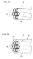
FIG. 19 is a perspective view illustrating an example of a litz wire. -
FIG. 20 is a perspective view illustrating an example of a high-frequency coil. -
FIG. 21 is a perspective view illustrating an example of a high-frequency coil. -
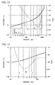
FIG. 22 is a diagram illustrating a test result. -
FIG. 23 is a diagram illustrating a test result. -
FIG. 17 is a cross-sectional view illustrating a high-frequency wire 10 (referred to as awire 10 below) according to an embodiment of the present invention. - The
wire 10 illustrated herein is a wire used for a specific frequency band. Thewire 10 includes aconductor portion 11. Theconductor portion 11 is formed from a two-layer structure conductor in which aninner layer 1 and anouter layer 2 are included. Theouter layer 2 is formed so as to cause an outer circumferential surface of theinner layer 1 to be coated with theouter layer 2. - The
inner layer 1 is formed of a material (material having volume resistivity higher than copper) which has lower conductivity than copper. As the material of theinner layer 1, metal having lower conductivity than copper may be used. The material of theinner layer 1 may be an insulating body. The material of theinner layer 1 may be a magnetic material or a non-magnetic material. Theinner layer 1 may have a cross-section shape which is circular. - The cross-section in the embodiment is referred to as a surface perpendicular to an axis direction of the
conductor portion 11. - As the material of the
inner layer 1, specifically, for example, an aluminium-containing material, an iron-containing material, a nickel-containing material, and the like are appropriate. - The
inner layer 1 is desirably formed of a homogeneous material. Theinner layer 1 may be formed of a composite material which is formed from a plurality of materials. However, in this case, conductivity (also referred to as electrical conductivity) may be obtained based on a cross-sectional area ratio of the plurality of materials. - As the aluminium-containing material, aluminium (Al) and aluminium alloys may be used. For example, aluminium for an electric use (EC aluminium), Al-Mg-Si-based alloys (within
JIS 6000 to 6999), and the like may be used. - A two-layer structure conductor in which the inner layer is formed from an aluminium wire, and the outer layer is formed from copper is referred to as a copper-coating aluminium wire.
- As the iron-containing material, iron (Fe) and iron alloys may be used. An example of the iron alloys includes a material containing one or more substances among carbon, silicon, nickel, tungsten, and chromium. For example, a steel wire, a stainless steel wire, or the like may be appropriately used as the
inner layer 1. - A two-layer structure conductor in which the inner layer is formed from a steel wire, and the outer layer is formed from copper is referred to as a copper-coating steel wire.
- As the nickel-containing material, nickel, nickel alloys, and the like may be used.
- As the nickel alloys, a nickel-chromium alloy is exemplified. In this case, for example, a nichrome wire may be used as the
inner layer 10. - A two-layer structure conductor in which the inner layer is formed from a nichrome wire, and the outer layer is formed from copper is referred to as a copper-coating nichrome wire.
- The
inner layer 1 is not limited to the exemplified materials. Pure metal such as magnesium, tungsten, titanium, and iron may be used for theinner layer 1. Copper alloys such as brass, phosphor bronze, silicon bronze, copper·beryllium alloys, and copper·nickel·silicon alloys may be used. In addition, an insulating body such as rubber and plastic may be used. - The
outer layer 2 is formed of copper. It is desirable that the cross-section area of theouter layer 2 be equal to or less than 50% with respect to the cross-section area of the entirety of theconductor portion 11 obtained by combining theinner layer 1 and theouter layer 2. Such a cross-sectional area ratio (cross-sectional area ratio of theouter layer 2 to the cross-section area of the entirety of the conductor portion 11) may be set to be 5% to 50%, for example. The cross-sectional area ratio of theouter layer 2 is set to be in the above range, and thus the cross-sectional area ratio of theouter layer 2 contributes to reduction of AC resistance. - The
outer layer 2 may have a constant thickness. - The diameter of the entirety of the wire 10 (diameter of the conductor portion 11) may be set to be 0.05 mm to 3.2 mm, for example.
- In the high-frequency wire according to the embodiment, in addition to the inner layer and the outer layer, one or more insulating layers of resin, ethylene, or the like may be formed on an outer circumferential side of the outer layer.
- Next, in order to describe a skin effect, electricity consumption in a case where an AC current is applied to the two-layer structure conductor is analyzed.
- As illustrated in
FIG. 16A , a two-layer structure conductor is modeled. In the two-layer structure conductor, the cross-section is circular, and layers are configured from materials different from each other, and are uniformly extended in a z-axis direction. An outer diameter of the i-th layer from the inside of the two-layer structure conductor is set as 2ri, conductivity thereof is set as σi, and relative magnetic permeability thereof is set as µi. A time factor is set as ejωt. µ0 indicates magnetic permeability in a vacuum. i is a natural number. j indicates an imaginary unit, and ω indicates an angular frequency defined as ω=2πf when f is set to indicate a frequency. - As illustrated in
FIG. 16B , when a current having amplitude of I flows in a z-axis direction of the lead wire, a z component Ez of an electric field satisfies the following wave equation.
- Since Expression (1) is the 0-th order Bessel equation, Expression (1) has the following solution.

- ki 2 is represented by the following expression.
- ki 2=-jωµ0µiσi
- Jn and Yn are respectively set to be the n-th order Bessel function and the n-th order Neumann function. Ai and Bi are constants determined by the following boundary conditions.
- A magnetic field is represented by the following expression, based on the Maxwell equation. The magnetic field Hθ indicates a component of a θ direction.

- A time average of electricity consumption of the lead wire having a length I is equal to a value obtained by integrating a pointing vector flowing from the surface of the lead wire, with the surface S of the lead wire. Thus, the time average is represented as follows.

P s : time average Li : internal inductance of unit length of conductor )
ζ is indicated by ζ=k2r2. - Resistance Rs and internal inductance Li when an AC current is applied to the two-layer structure conductor having a unit length are represented by the following expression.
- It is desirable that the frequency of the AC current be a frequency in a specific frequency region which is defined (set) as a range in which the wire (product) is used.

- When σ1=σ2 and µ1=µ2, A2=1 and B2=0 are set and Rs in Expression (5) is represented by the following expression.

- The layers are magnetic substances. In a case where magnetic loss is indicated by magnetic hysteresis and the like, the loss may be indicated by introducing an imaginary part into magnetic permeability. For example, the following expression is established.

- Next, in order to describe a proximity effect, electricity consumption in a case where an AC magnetic field is uniformly applied to the two-layer structure conductor from the outside is analyzed.
- As illustrated in
FIG. 16A , if a vector potential satisfying H=∇×A is introduced, the vector potential A2=H0rsinθ in the z-axis direction is applied to a magnetic field having uniform amplitude H0 from an x-axis direction. - When the magnetic field is caused to react with the lead wire, Az satisfies the following wave equation.

- Expression (8) has the following solution.

- Ci and Di are constants determined by the following boundary conditions.

- The magnetic field and the electric field are represented by the following expression by using Expression (9).

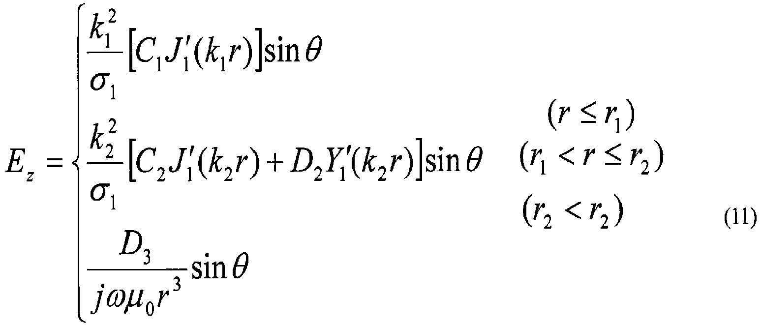
- At this time, since electricity consumption in the lead wire is equal to a real part of a value obtained by integrating a pointing vector flowing from the surface of the lead wire, with the surface S of the lead wire, when the magnetic field having amplitude H0 is caused to react, the time average of eddy current loss occurring in the lead wire having a length I is represented by the following expression.


P p :time average Lm :mutual internal inductance of unit length of conductor) - Since a near magnetic field of a coil is generated by a current I flowing in the coil, the amplitude H0 of the magnetic field is proportional to the amplitude of I. If the proportional coefficient is set as α, H0 is represented as follows.

- Thus, resistance Rp by the proximity effect is represented as follows.

- Dp is represented as follows.

- When σ1=σ2 and µ1=µ2 are set, C2=1 and D2=0 are set, and Expression (15) is represented by the following expression.

- AC resistance Rac of the coil or the cable is represented as the sum of resistance Rs by electrification and resistance Rp by the proximity effect.

- In this manner, Rs and Dp are formulated, and thus a lead wire which is a two-layer structure conductor of which the outer layer is configured by copper, and a lead wire (copper wire) formed from copper are compared to each other regarding the skin effect and the proximity effect.
- Regarding a two-layer structure conductor (copper-coating aluminium wire) (Example 1), a two-layer structure conductor (copper-coating steel wire) (Example 2), and a two-layer structure conductor (copper-coating nichrome wire) (Example 3), the following calculation was performed. In the copper-coating aluminium wire (Example 1), the inner layer was formed by an alloy aluminium wire, and the outer layer was formed by copper.
In the copper-coating steel wire (Example 2), the inner layer was formed by a steel wire and the outer layer was formed by copper. In the copper-coating nichrome wire (Example 3), the inner layer was formed by a nickel wire, and the outer layer was formed by copper. - For comparison, similar calculation was performed on a copper wire having a single-layer structure (one-layer structure) (Comparative Example 1). The copper wire may have a cross-section which is circular. The single-layer structure is referred to as a structure formed from a homogeneous material.
- In the following descriptions, the two-layer structure conductor or the copper wire may be singly referred to as a "lead wire". In addition, alloy aluminium may be singly referred to as "aluminium".
- The outer diameter of the lead wires (Examples 1 to 3 and Comparative Example 1) was set to 1.0 mm. In Examples 1 to 3 (two-layer structure conductors), the cross-sectional area ratio of the outer layer to the entirety of the lead wire was set to 25%.
- Regarding the two-layer structure conductors in Examples 1 to 3 and Comparative Example 1, resistance Rs and internal inductance Li shown in the abovementioned Expression (5) were obtained by calculation. Dp shown in the abovementioned Expression (15) was obtained by calculation.
- With the calculation, volume resistivity (20°C) of copper was set to 1.72×10⁻⁸ [Ω·m], volume resistivity (20°C) of alloy aluminium was set to 3.02×10⁻⁸ [Ω·m], volume resistivity (20°C) of steel was set to 1.57×10⁻⁷ [Ω·m], and volume resistivity (20°C) of nichrome was set to 1.50×10⁻⁶ [Ω·m]. The volume resistivity of alloy aluminium referred to an I-aluminium alloy wire (JEC-3405, standard of Electrical Standards Committee in Institute of Electrical Engineering). The conductivity (20°C) of copper was set to 5.8×10⁷ [Ω-1·m-1], the conductivity (20°C) of alloy aluminium was set to 3.3×10⁷ [Ω·m-1], the conductivity (20°C) of steel was set to 6.4×10⁶ [Ω-1·m-1], and the conductivity (20°C) of nichrome was set to 6.6×10⁶ [Ω-1·m-1].
- Relative magnetic permeability of copper was set to 1, the relative magnetic permeability of alloy aluminium was set to 1, the relative magnetic permeability of steel was set to 100, and the relative magnetic permeability of nichrome was set to 1.
-
FIG. 1 illustrates a calculation result of the resistance Rs. The resistance Rs in Examples 1 to 3 (two-layer structure conductors) was lower than that in Comparative Example 1 (copper wire), in a range in which a frequency was higher than a first frequency (about 1.2 MHz) and less than a second frequency (about 7.1 MHz) which was higher than the first frequency. - That is, the resistance Rs in Examples 1 to 3 (two-layer structure conductors) was higher than the resistance Rs in Comparative Example 1 (copper wire) on a lower frequency side than the first frequency. The resistance Rs in Examples 1 to 3 and the resistance Rs in Comparative Example 1 matched each other at the first frequency. The resistance Rs in Examples 1 to 3 was lower than the resistance Rs in Comparative Example 1, in a range in which a frequency was on a higher frequency side than the first frequency and was less than the second frequency. The resistance Rs in Examples 1 to 3 and the resistance Rs in Comparative Example 1 matched each other again at the second frequency. The resistance Rs in Examples 1 to 3 was higher than the resistance Rs in Comparative Example 1, on a higher frequency side than the second frequency.
-
FIG. 2 illustrates a calculation result of Dp. Dp in Examples 1 to 3 (two-layer structure conductors) was lower than Dp in Comparative Example 1 (copper wire), in a range in which a frequency was higher than a first frequency (about 1.5 MHz) and less than a second frequency (about 7.1 MHz) which was higher than the first frequency. - That is, Dp in Examples 1 to 3 (two-layer structure conductors) was higher than Dp in Comparative Example 1 (copper wire) on a lower frequency side than the first frequency. Dp in Examples 1 to 3 and Dp in Comparative Example 1 matched each other at the first frequency. Dp in Examples 1 to 3 was lower than Dp in Comparative Example 1, in a range in which a frequency was on a higher frequency side than the first frequency and was less than the second frequency. Dp in Examples 1 to 3 and Dp in Comparative Example 1 matched each other again at the second frequency. Dp in Examples 1 to 3 was higher than Dp in Comparative Example 1, on a higher frequency side than the second frequency.
-
FIG. 3 illustrates a calculation result of the internal inductance Li. Li in Examples 1 to 3 (two-layer structure conductors) was higher than Li in Comparative Example 1 (copper wire), in a range in which a frequency was on a higher frequency than a first frequency (about 3.6 MHz) and less than a second frequency (about 10 MHz) which was higher than the first frequency. - That is, the internal inductance Li in Examples 1 to 3 (two-layer structure conductors) was lower than Li in Comparative Example 1 (copper wire) on a lower frequency side than the first frequency. Li in Examples 1 to 3 and Li in Comparative Example 1 matched each other at the first frequency. Li in Examples 1 to 3 was higher than Li in Comparative Example 1, in a range in which a frequency was on the higher frequency side than the first frequency and was less than the second frequency. Li in Examples 1 to 3 and Li in Comparative Example 1 matched each other again at the second frequency. Li in Examples 1 to 3 was lower than Li in Comparative Example 1, on a higher frequency side than the second frequency.
-
FIG. 4 is a diagram illustrating a ratio (Examples 1 to 3/Comparative Example 1) of the resistance Rs between Examples 1 to 3 and Comparative Example 1 (copper wire), for easy understanding of the calculation result illustrated inFIG. 1 . The following are understood based onFIG. 4 . - In Example 1 (copper-coating aluminium wire), the resistance Rs could be reduced by about 1%, which was the maximum, in comparison to Comparative Example 1 (copper wire).
- In Example 2 (copper-coating steel wire), the resistance Rs could be reduced by approximately 7%, which was the maximum, in comparison to Comparative Example 1 (copper wire).
- In Example 3 (copper-coating nichrome wire), the resistance Rs could be reduced by approximately 7%, which was the maximum, in comparison to Comparative Example 1 (copper wire).
-
FIG. 5 is a diagram illustrating a ratio (Examples 1 to 3/Comparative Example 1) of Dp between Examples 1 to 3 and Comparative Example 1 (copper wire), for easy understanding of the calculation result illustrated inFIG. 2 . The following are understood based onFIG. 5 . - In Example 1 (copper-coating aluminium wire), Dp could be reduced by about 1%, which was the maximum, in comparison to Comparative Example 1 (copper wire).
- In Example 2 (copper-coating steel wire), Dp could be reduced by approximately 7%, which was the maximum, in comparison to Comparative Example 1 (copper wire).
- In Example 3 (copper-coating nichrome wire), Dp could be reduced by approximately 7%, which was the maximum, in comparison to Comparative Example 1 (copper wire).
-
FIG. 6 is a diagram illustrating a ratio (Examples 1 to 3/Comparative Example 1) of the internal inductance Li between Examples 1 to 3 and Comparative Example 1 (copper wire), for easy understanding of the calculation result illustrated inFIG. 3 . The following are understood based onFIG. 6 . - In Example 1 (copper-coating aluminium wire), the internal inductance Li could be increased by approximately 0.3%, which was the maximum, in comparison to Comparative Example 1 (copper wire).
- In Example 2 (copper-coating steel wire), the internal inductance Li could be increased by approximately 2%, which was the maximum, in comparison to Comparative Example 1 (copper wire).
- In Example 3 (copper-coating steel wire), the internal inductance Li could be increased by approximately 2%, which was the maximum, in comparison to Comparative Example 1 (copper wire).
- A two-layer structure conductor (copper-coating steel wire) was similar to that in Example 2 except that the cross-sectional area ratio of the outer layer was set to 75%. Regarding the two-layer structure conductor (copper-coating steel wire), the ratio of Rs, the ratio of Dp, and the ratio of Li to Rs, Dp, and Li in Comparative Example 1 (copper wire) were obtained.
FIG. 7A illustrates a result. - In
FIG. 7A , the ratio of Rs to Rs in Comparative Example 1 (copper wire) was marked as "Rs (75%CS/Cu)", the ratio of Dp to Dp in Comparative Example 1 (copper wire) was marked as "Dp (75%CS/Cu)", and the ratio of Li to Li in in Comparative Example 1 (copper wire) was marked as "Li (75%CS/Cu)". - Regarding Example 2, the ratio of Rs, the ratio of Dp, and the ratio of Li to Rs, Dp, and Li in Comparative Example 1 (copper wire) were also obtained.
FIG. 7A illustrates a result. - In
FIG. 7A , the ratio of Rs to Rs in Comparative Example 1 (copper wire) was marked as "Rs (25%CS/Cu)", the ratio of Dp to Dp in Comparative Example 1 (copper wire) was marked as "Dp (25%CS/Cu)", and the ratio of Li to Li in in Comparative Example 1 (copper wire) was marked as "Li (25%CS/Cu)". - A two-layer structure conductor (copper-coating steel wire) was similar to that in Example 2 except that the cross-sectional area ratio of the outer layer was set to 5%. Regarding the two-layer structure conductor (copper-coating steel wire), the ratio of Rs, the ratio of Dp, and the ratio of Li to Rs, Dp, and Li in Comparative Example 1 (copper wire) were obtained.
FIG. 7A illustrates a result. - In
FIG. 7A , the ratio of Rs to Rs in Comparative Example 1 (copper wire) was marked as "Rs (5%CS/Cu)", the ratio of Dp to Dp in Comparative Example 1 (copper wire) was marked as "Dp (5%CS/Cu)", and the ratio of Li to Li in in Comparative Example 1 (copper wire) was marked as "Li (5%CS/Cu)". - As illustrated in
FIG. 7A , Rs in Example 4 (copper-coating steel wire) is smaller than Rs in Comparative Example 1 (copper wire), in a frequency region A1. For this reason, Example 4 has an advantage of Rs over Comparative Example 1 in the frequency region A1. - Since Dp in Example 4 is smaller than Dp in Comparative Example 1 in the frequency region A1, Example 4 has an advantage of Dp over Comparative Example 1 in the frequency region A1.
- In a frequency region B1, which is a region in the frequency region A1 and is narrower than the frequency region A1, since Li in Example 4 is greater than Li in Comparative Example 1, Example 4 has an advantage of Li over Comparative Example 1 in the frequency region A1.
- As described above, Example 4 has advantages of Rs and Dp in the frequency region A1, and also has an advantage of Li in the frequency region B1, which is narrower than the region A1.
- As illustrated in
FIG. 7B , Example 2 has advantages of Rs and Dp in a frequency region A2, and also has an advantage of Li in a frequency region B2, which is narrower than the region A2. - As illustrated in
FIG. 7C , Example 5 has advantages of Rs and Dp in a frequency region A3, and also has an advantage of Li in a frequency region B3, which is narrower than the region A3. - The result of Rs, Dp, and Li may be considered as follows.
-
FIGS. 8A to 8C are diagrams illustrating a real part of current density distribution in a radial direction of a copper-coating nichrome wire when a current having a frequency of 1 kHz (FIG. 8A ), 3 MHz (FIG. 8B ), or10 MHz (FIG. 8C ) flows into the copper-coating nichrome wire (Example 3, cross-sectional area ratio of outer layer: 25%, outer diameter: 1.0 mm). - The current density distribution for Comparative Example 1 (copper wire) was similarly calculated.
- The current density distribution was calculated by multiplying conductivity by Expression (2).
- In
FIG. 8A , the current uniformly flows in a positive direction, at 1 kHz, and most of the current flows only into the outer layer (copper) of the copper-coating nichrome wire. For this reason, it is understood that the effective cross-section area in which the current flows in the copper-coating nichrome wire is smaller than that in the copper wire, and the current distribution has large deviation. - Since the loss has a square function of a current, the loss is increased as the deviation of the current distribution becomes larger. For this reason, the copper-coating nichrome wire has larger resistance than the copper wire.
- In
FIG. 8B , it is understood that a portion of the current flowing the copper wire flows into the inside thereof in a negative direction (that is, reflux is caused) at 3 MHz, but, in the copper-coating nichrome wire, the reflux is not caused. - Since the reflux is caused in the copper wire, the current in the positive direction is largely deviated, and thus the resistance is larger than that of the copper-coating nichrome wire.
- In
FIG. 8C , the reflux is also caused in the outer layer of a copper-nichrome wire, at 10 MHz. The current density distribution of the copper-nichrome wire is approximate to the current density distribution of the copper wire. - It is understood that the reflux is caused in the copper wire in a frequency region including 3 MHz, and the current is concentrated on a portion corresponding to the outer layer, and thus the loss in the copper-nichrome wire is smaller than the loss in the copper wire, based on the results.
- As described above, in the two-layer structure conductor in which the inner layer is formed from a material having lower conductivity than copper, and the outer layer is formed from copper, it is possible to suppress an increase of resistance in a specific frequency region, in comparison to that of the copper wire. Accordingly, it is possible to improve the Q value of a coil.
-
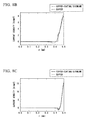
FIGS. 9A to 9C are diagrams illustrating an absolute value of eddy current density on a surface which is perpendicular to an external magnetic field and passes through the center of a lead wire (copper-coating nichrome wire) when a uniform magnetic field is applied to the copper-coating nichrome wire (Example 3, cross-sectional area ratio of outer layer: 25%, outer diameter: 1.0 mm) from the outside thereof. -
FIG. 9A illustrates an absolute value of eddy current density in a case where the frequency of the magnetic field is 500 kHz.FIG. 9B illustrates an absolute value of eddy current density in a case where the frequency of the magnetic field is 2 MHz.FIG. 9C illustrates an absolute value of eddy current density in a case where the frequency of the magnetic field is 10 MHz. - The absolute value of the eddy current density for Comparative Example 1 (copper wire) was similarly calculated.
- The current density distribution was calculated by multiplying conductivity by Expression (11).
- In
FIG. 9A , it is understood that an eddy current in the copper-coating nichrome wire flows into the outer layer at 500 kHz, and thus the current density distribution in the copper-coating nichrome wire is deviated larger than that of the copper wire. - In
FIG. 9B , it is understood that the current density of the copper wire on the surface of the lead wire is denser than that of the copper-coating nichrome wire, at 2 MHz, and thus the current density distribution in the copper wire is deviated larger than that in the copper-coating nichrome wire. - In
FIG. 9C , it is understood that the current density distribution of the copper-nichrome wire is approximate to the current density distribution of the copper wire at 10 MHz. - It is understood that deviation of the eddy current in the copper wire is larger than deviation of the eddy current in the copper-coating nichrome wire in a frequency region including 2 MHz, and thus the loss in the copper-nichrome wire is smaller than the loss in the copper wire, based on the results.
- As described above, in the two-layer structure conductor in which the outer layer is formed from copper and the inner layer is configured by a material having lower conductivity than copper (material having high volume resistivity), it is possible to suppress an increase of eddy current loss in a specific frequency region, in comparison to that of the copper wire.
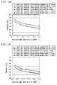
- In a copper-coating aluminium wire (Example 6), a copper-coating steel wire (Example 7), and a copper-coating nichrome wire (Example 8) which were two-layer structure conductors having an outer diameter of 0.1 mm, 1.0 mm, or 3.2 mm, a frequency region in which the resistance Rs was smaller than the resistance Rs of the copper wire was obtained by simulation.
- The cross-sectional area ratio of the outer layer was set to 5%, 15%, 25%, and 50%.
-
FIGS. 10A to 10C illustrate the lower limit value and the upper limit value of the obtained frequency region. -
FIGS. 10A to 10C respectively illustrate results of cases where the outer diameter is 0.1 mm, 1.0 mm, and 3.2 mm. - As illustrated in
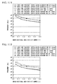
FIGS. 10A to 10C , if the cross-sectional area ratio of the outer layer (copper) is changed, the frequency region in which Rs of the two-layer structure conductor is smaller than Rs of the copper wire is changed. For this reason, it is possible to reduce the resistance of the two-layer structure conductor in comparison to that of the copper wire in a wide frequency region by adjusting the cross-sectional area ratio of the outer layer (copper). Accordingly, it is possible to improve the Q value of a coil. - In the copper-coating aluminium wire (Example 6), the copper-coating steel wire (Example 7), and the copper-coating nichrome wire (Example 8), a frequency region in which the resistance Rs was smaller than the resistance Rs of the copper wire and Dp was smaller than Dp of the copper wire was obtained by simulation.
-
FIGS. 11A to 11C illustrate the lower limit value and the upper limit value of the obtained frequency region. -
FIGS. 11A to 11C respectively illustrate results of cases where the outer diameter is 0.1 mm, 1.0 mm, and 3.2 mm. - As illustrated in
FIGS. 11A to 11C , if the cross-sectional area ratio of the outer layer (copper) is changed, the frequency region in which the resistance Rs of the two-layer structure conductor is smaller than the resistance Rs of the copper wire and Dp of the two-layer structure conductor is smaller than Dp of the copper wire is changed. For this reason, it is possible to reduce the resistance and the proximity effect of the two-layer structure conductor in comparison to those of the copper wire in a wide frequency region by adjusting the cross-sectional area ratio of the outer layer (copper). Accordingly, it is possible to improve the Q value of a coil. - In the copper-coating aluminium wire (Example 6), the copper-coating steel wire (Example 7), and the copper-coating nichrome wire (Example 8), a frequency region in which Rs was smaller than Rs of the copper wire and Dp was smaller than Dp of the copper wire, but the internal inductance Li was larger than the internal inductance Li of the copper wire was obtained by simulation.
-
FIGS. 12A to 12C illustrate the lower limit value and the upper limit value of the obtained frequency region. -
FIGS. 12A to 12C respectively illustrate results of cases where the outer diameter is 0.1 mm, 1.0 mm, and 3.2 mm. - As illustrated in
FIGS. 12A to 12C , if the cross-sectional area ratio of the outer layer (copper) is changed, the frequency region in which Rs is smaller than Rs of the copper wire and Dp is smaller than Dp of the copper wire, but Li is larger than Li of the copper wire is changed. - For this reason, it is possible to reduce the resistance and the proximity effect of the two-layer structure conductor and to increase the internal inductance of the two-layer structure conductor, in comparison to those of the copper wire in a wide frequency region by adjusting the cross-sectional area ratio of the outer layer (copper).
- Accordingly, it is possible to improve the Q value of a coil.
- Table 1 to Table 3 show (1) the lower limit value and the upper limit value of a frequency region in which the resistance Rs is smaller than the resistance Rs of the copper wire, (2) the lower limit value and the upper limit value of a frequency region in which Rs is smaller than Rs of the copper wire and Dp is smaller than Dp of the copper wire, and (3) the lower limit value and the upper limit value of a frequency region in which Rs is smaller than Rs of the copper wire and Dp is smaller than Dp of the copper wire, but the internal inductance Li is larger than the internal inductance Li of the copper wire, regarding the copper-coating aluminium wire (Example 6), the copper-coating steel wire (Example 7), and the copper-coating nichrome wire (Example 8).
- [Table 1]
Wire diameter 0.1 mmφ 0.4 mmφ Wire type Copper-coating aluminium wire Copper-coating steel wire Copper-coating nichrome wire Copper-coating aluminium wire Copper-coating steel wire Copper-coating nichrome wire Coverage of copper Lower limit frequency [kHz] Upper limit frequency [kHz] Lower limit frequency [kHz] Upper limit frequency [kHz] Lower limit frequency [kHz] Upper limit frequency [kHz] Lower limit frequency [kHz] Upper limit frequency [kHz] Lower limit frequency [kHz] Upper limit frequency [kHz] Lower limit frequency [kHz] Upper limit frequency [kHz] Only Rs 0.5 19600 137000 27300 152000 26500 148000 1220 8590 1700 9500 1650 9290 0.25 126000 665000 127000 724000 119000 712000 7970 41600 8000 45200 7510 44500 0.15 385000 1960000 375000 2130000 355000 2110000 24000 123000 23400 133000 22100 132000 0.05 3740000 20500000 3560000 20600000 3550000 20500000 233000 1280000 222000 1280000 221000 1280000 Rs and Dp 0.5 33600 137000 35000 152000 42400 148000 2100 8590 2180 9500 2650 9290 0.25 143000 665000 142000 724000 153000 712000 8990 41600 8980 45200 9630 44500 0.15 411000 1960000 402000 2130000 407000 2110000 25600 123000 25100 133000 25400 132000 0.05 3820000 20500000 3640000 20600000 3640000 20500000 238000 1280000 227000 1280000 227000 1280000 Rs, Dp, and Li 0.5 75200 137000 79700 152000 77700 148000 4700 8590 4980 9500 4850 9290 0.25 369000 665000 377000 724000 364000 712000 23000 41600 23500 45200 22700 44500 0.15 1090000 1960000 1100000 2130000 1090000 2110000 68700 123000 69500 133000 68600 132000 0.05 10600000 20500000 10600000 20600000 10600000 20500000 658000 1280000 660000 1280000 657000 1280000 -
Wire diameter 1.0 mmφ 1.8 mmφ Wire type Copper-coating minium wire Copper-coating steel wire Copper-coating nichrome wire Copper-coating aluminium wire Copper-coating steel wire Copper-coating nichrome wire Coverage of copper Lower limit frequency [kHz] Upper limit frequency [kHz] Lower limit frequency [kHz] Upper limit frequency [kHz] Lower limit frequency [kHz] Upper limit frequency [kHz] Lower limit frequency [kHz] Upper limit frequency [kHz] Lower limit frequency [kHz] Upper limit frequency [kHz] Lower limit frequency [kHz] Upper limit frequency [kHz] Only Rs 0.5 196 1380 216 1450 265 1480 60.8 424 84.4 469 82 459 0.25 1260 6660 1260 6650 1190 7120 393 2050 394 2230 370 2190 0.15 3850 19700 3740 20800 3550 21100 1180 6070 1150 6580 1090 6530 0.05 37400 188000 37400 187000 35500 201000 11500 57900 11100 62300 10900 62300 Rs and Dp 0.5 336 1380 385 1450 424 1480 103 424 107 469 130 459 0.25 1430 6660 1430 6650 1530 7120 443 2050 443 2230 475 2190 0.15 4110 19700 4020 20800 4070 21100 1260 6070 1230 6580 1240 6530 0.05 38200 188000 38200 187000 36400 201000 11700 57900 11300 62300 11100 62300 Rs, Dp, and L 0.5 752 1380 726 1450 777 1480 231 424 245 469 239 459 0.25 3690 6660 3690 6650 3640 7120 1130 2050 1150 2230 1110 2190 0.15 10900 19700 10800 20800 10900 21100 3390 6070 3420 6580 3380 6530 0.05 104000 188000 104000 187000 104000 201000 32400 57900 34500 62300 32400 62300 [Table 3] Wire diameter 2.5 mmφ 3.2 mmφ Wire type Copper-coating aluminium wire Copper-coating steel wire Copper-coating nichrome wire Copper-coating aluminium wire Copper-coating steel wire Copper-coating nichrome wire Coverage of copper Lower limit frequency [kHz] Upper limit frequency [kHz] Lower limit frequency [kHz] Upper limit frequency [kHz] Lower limit frequency [kHz] Upper limit frequency [kHz] Lower limit frequency [kHz] Upper limit frequency [kHz] Lower limit frequency [kHz] Upper limit frequency [kHz] Lower limit frequency [kHz] Upper limit frequency [kHz] Only Rs 0.5 31.4 220 43.7 243 42.4 237 19.1 134 26.6 148 25.8 145 0.25 203 1060 204 1150 191 1140 123 650 124 707 116 696 0.15 618 3150 601 3410 569 3380 376 1920 366 2080 347 2060 0.05 6000 30000 5710 32300 5690 32300 3660 18300 3480 19700 3470 19700 Rs and Dp 0.5 53.9 220 56.1 243 68 237 32.8 134 34.2 148 41.4 145 0.25 0.15 229 659 1060 3150 229 644 1150 3410 245 652 1140 3380 139 402 650 1920 139 392 707 2080 149 397 696 2060 0.05 6120 30000 5830 32300 5830 32300 3730 18300 3560 19700 3550 19700 Rs, Dp, and Li 0.5 119 220 126 243 123 237 73.5 134 77.8 148 75.9 145 0.25 592 1060 604 1150 583 1140 361 650 368 707 355 696 0.15 1750 3150 1770 3410 1750 3380 1060 1920 1070 2080 1060 2060 0.05 16700 30000 16800 32300 16700 32300 10200 18300 11000 19700 10100 19700 - The reason that Rs, Dp, and Li of the two-layer structure conductor are different from Rs, Dp, and Li of the copper wire is because flowing of the current into the inner layer having low conductivity is difficult, and thus the current distribution by the skin effect is different between the two-layer structure conductor and the copper wire.
- The lower limit frequency and the upper limit frequency of the above-described frequency region may be determined in association with the skin thickness δ [m] in a copper wire which functions as a reference.
- The "copper wire which functions as a reference" includes a conductor portion formed from pure copper (formed only by pure copper). It is preferable that the copper wire have a wire diameter the same as that of the two-layer structure conductor. However, the copper wire may have a different wire diameter.
-
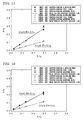
FIG. 13 illustrates a correlation between a ratio of the skin thickness δ of the copper wire and the radius r2 of the two-layer structure conductor, and a ratio of the thickness t of the outer layer (copper) in the two-layer structure conductor and the radius r2 of the two-layer structure conductor, at the lower limit frequency and the upper limit frequency of a frequency region in which Rs of the two-layer structure conductor is smaller than Rs of the copper wire. - Regression analysis was performed on the results by using a linear function, thereby a regression analysis straight line illustrated in
FIG. 13 was obtained. The solid line indicates a regression analysis straight line for the lower limit frequency, and the broken line indicates a regression analysis straight line of the upper limit frequency. - The skin thickness δ [m] of the copper wire is represented by the following Expression (18).

- In a case of the lower limit frequency, the thickness t of the outer layer (copper) in the two-layer structure conductor was 0.92 times the skin thickness δ of the copper wire. In a case of the upper limit frequency, the thickness t was 0.37 times the skin thickness δ.
- For this reason, when the thickness t [m] of the outer layer (copper) is in a range of the following Expression (19), Rs of the two-layer structure conductor is smaller than Rs of the copper wire. Accordingly, it is possible to improve the Q value of a coil.

- With the Expression (18), if the conductivity of copper is set to 5.8×10⁷ [Ω-1·m-1], and the magnetic permeability of copper is set to 4π×10-7 [H/m], which is equal to the magnetic permeability of a vacuum, t [m] given in Expression (19) is represented as in the following Expression (20) as a relational expression depending on a frequency f [Hz].

-
FIG. 14 illustrates a correlation between a ratio of the skin thickness δ of the copper wire and the radius r2 of the two-layer structure conductor, and a ratio of the thickness t of the outer layer (copper) in the two-layer structure conductor and the radius r2 of the two-layer structure conductor, at the lower limit frequency and the upper limit frequency of a frequency region in which Rs of the two-layer structure conductor is smaller than Rs of the copper wire, and Dp of the two-layer structure conductor is smaller than Dp of the copper wire. - Regression analysis was performed on the results by using a linear function, thereby a regression analysis straight line illustrated in
FIG. 14 was obtained. The solid line indicates a regression analysis straight line for the lower limit frequency, and the broken line indicates a regression analysis straight line of the upper limit frequency. - In a case of the lower limit frequency, the thickness t of the outer layer (copper) in the two-layer structure conductor was 0.76 times the skin thickness δ of the copper wire. In a case of the upper limit frequency, the thickness t was 0.37 times the skin thickness δ.
- For this reason, when the thickness t [m] of the outer layer (copper) is in a range of the following Expression (21), Rs of the two-layer structure conductor is smaller than Rs of the copper wire and Dp is smaller than Dp of the copper wire. Accordingly, it is possible to improve the Q value of a coil.

- With the Expression (18), if the conductivity of copper is set to 5.8×10⁷ [Ω-1·m-1], and the magnetic permeability of copper is set to 4π×10-7 [H/m], which is equal to the magnetic permeability of a vacuum, t [m] given in Expression (21) is represented as in the following Expression (22) as a relational expression depending on a frequency f [Hz].

-
FIG. 15 illustrates a correlation between a ratio of the skin thickness δ of the copper wire and the radius r2 of the two-layer structure conductor, and a ratio of the thickness t of the outer layer (copper) in the two-layer structure conductor and the radius r2 of the two-layer structure conductor, at the lower limit frequency and the upper limit frequency of a frequency region in which Rs of the two-layer structure conductor is smaller than Rs of the copper wire, and Dp of the two-layer structure conductor is smaller than Dp of the copper wire, but Li is larger than Li of the copper wire. - Regression analysis was performed on the results by using a linear function, thereby a regression analysis straight line illustrated in
FIG. 15 was obtained. The solid line indicates a regression analysis straight line for the lower limit frequency, and the broken line indicates a regression analysis straight line of the upper limit frequency. - In a case of the lower limit frequency, the thickness t of the outer layer (copper) in the two-layer structure conductor was 0.51 times the skin thickness δ of the copper wire. In a case of the upper limit frequency, the thickness t was 0.37 times the skin thickness δ.
- For this reason, when the thickness t [m] of the outer layer (copper) is in a range of the following Expression (23), Rs of the two-layer structure conductor is smaller than Rs of the copper wire and Dp is smaller than Dp of the copper wire, but Li is larger than Li of the copper wire. Accordingly, it is possible to improve the Q value of a coil.

- With the Expression (18), if the conductivity of copper is set to 5.8×10⁷ [Ω-1·m-1], and the magnetic permeability of copper is set to 4π×10-7 [H/m], which is equal to the magnetic permeability of a vacuum, t [m] given in Expression (23) is represented as in the following Expression (24) as a relational expression depending on a frequency f [Hz].

- Generally, the frequency of a current flowing in a cable or a coil is determined by an external factor of equipment using the current, and the like. Examples of equipment to be used include an induction heating device, a non-contact feeding device, a plasma-generating device, a switching power source, a microwave filter, an antenna, and facilities attached to the above-described device.
- When the frequency is determined, the thickness of the lead wire is determined by a factor relating to the size, balance between Rs and Dp, or the like. If the frequency and the thickness of the lead wire are determined, the thickness and the cross-sectional area ratio of the outer layer (copper) are selected in accordance with Expression (19), and thus it is possible to reduce resistance in comparison to that of the copper wire.
- In a case where ignoring of an influence of the proximity effect is not possible, the thickness and the cross-sectional area ratio of the outer layer (copper) are selected in accordance with Expression (21), and thus it is possible to reduce both of the resistance and the proximity effect in comparison to that of the copper wire.
- In a case where the Q value of a coil is increased, the thickness and the cross-sectional area ratio of the outer layer (copper) are selected in accordance with Expression (23), and thus it is possible to increase apparent electric power with respect to the electricity consumption of the coil.
- The wire of the present invention may have a structure in which the outer layer is formed from copper, and the inner layer is formed from a material having lower conductivity than that of copper (that is, material having high volume resistivity. For example, metal or an insulating body having lower conductivity than that of copper). The material for forming the inner layer is not limited the exemplified materials.
-
FIG. 18 illustrates awire 10A which is a modification example of thewire 10. In thewire 10A, aninsulation coating layer 3 is provided on an outer circumferential surface of a conductor portion 11 (on an outer circumferential surface of an outer layer 2). Theinsulation coating layer 3 coats the outer circumferential surface of theconductor portion 11. Theinsulation coating layer 3 is the outermost layer of thewire 10A. - The
insulation coating layer 3 may be formed by coating with an enamel coating material such as polyester, polyurethane, polyimide, polyester imide, polyamide-imide, and the like. Thewire 10A in which theinsulation coating layer 3 is formed by using the enamel coating material is an enamel wire. -
FIG. 19 illustrates alitz wire 60 which is an example of a litz wire which uses thewire 10A illustrated inFIG. 18 . Thelitz wire 60 is configured to have a plurality ofwires 10A which are bundled and twisted. -
FIG. 20 illustrates acable 80 which is an example of a cable in which insulation coating is performed on thelitz wire 60. In thecable 80, aninsulation coating layer 81 formed of polyethylene and the like is provided on an outer circumferential surface of thelitz wire 60. -
FIG. 21 illustrates acoil 70 which is an example of a coil (high-frequency coil) which uses thewire 10A illustrated inFIG. 18 . Thecoil 70 includes thewire 10A and asupport body 73. Thesupport body 73 includes abody portion 71 andflange portions 72 which are formed at both ends of thebody portion 71. - The
wire 10A is wound around thebody portion 71. - The
coil 70 may use thelitz wire 60 illustrated inFIG. 19 , instead of thewire 10A or thecable 80 may be used as thecoil 70. - A coil (number of winding of 3) was manufactured by using a copper-coating aluminium wire (cross-sectional area ratio of outer layer: 25%, outer diameter: 1.8 mm), and AC resistance was measured.
FIG. 22 illustrates a result. - For comparison, similar calculation was performed on a copper wire having a single-layer structure (Comparative Example 2).
- In
FIG. 22 , the copper-coating aluminium wire was marked as "CA" and the copper wire was marked as "Cu". The ratio (copper-coating aluminium wire/copper wire) of Rs was set as "CA/Cu". - As illustrated in
FIG. 22 , in a frequency region A4, Rs in Example 9 (copper-coating aluminium wire) was less than Rs in Comparative Example 2 (copper wire), and the ratio (copper-coating aluminium wire/copper wire) (CA/Cu) of Rs was smaller than 1. - A coil (number of winding of 1) was manufactured by using a copper-coating steel wire (cross-sectional area ratio of outer layer: 25%, outer diameter: 2.0 mm), and AC resistance was measured.
FIG. 23 illustrates a result. - In
FIG. 23 , the copper-coating steel wire was marked as "CS" and the copper wire was marked as "Cu". The ratio (copper-coating steel wire/copper wire) of Rs was set as "CS/Cu". - As illustrated in
FIG. 23 , in a frequency region A5, Rs in Example 10 (copper-coating steel wire) was less than Rs in Comparative Example 2 (copper wire), and the ratio of Rs was smaller than 1. - Subsequently, an example of a method of manufacturing the
wire 10 will be described. - A copper tape is vertically attached to a surface of an inner layer body formed from aluminium alloys, steel, nichrome alloys, and the like, for example. A result of attachment is subjected to TIG welding, plasma welding, or the like. Thus, an outer layer formed from copper is formed on an outer circumferential surface of the inner layer body, and a material obtained by the formation is set as a base material. The base material is subjected to wire drawing through a wire drawing die having a plurality of stages, and thus the
wire 10 which includes theinner layer 1 and theouter layer 2 may be obtained. - The base material obtained by inserting the inner layer body formed by aluminium alloys and the like into a copper tube is subjected to wire drawing through a wire drawing die having a plurality of stages, and thus the
wire 10 which includes theinner layer 1 and theouter layer 2 may be obtained. The copper tube is manufactured by using a general tube manufacturing method. - The
outer layer 2 may be formed on an outer circumferential surface of theinner layer 1 by copper plating. - The manufacturing method described herein does not limit the scope of the present invention. The high-frequency wire according to the embodiment of the present invention can also be manufactured by a manufacturing method other than the method exemplified herein.
- The above-described embodiments have exemplified a device and a method in order to materialize the technical ideas of the invention. Therefore, in the technical ideas of the invention, the material properties, the shapes, the structures, the arrangements, and the like of the configurational components are not specified. The present invention does not exclude a structure in which a third layer is included in addition to the inner layer and the outer layer. As the regression analysis by using the above-described linear function, a least squares method may be employed.
- A high-frequency wire and a high-frequency coil of the present invention can be utilized in the electronic equipment industry including the industry of manufacturing various devices such as a non-contact feeding device, a high-frequency current generation device, and the like including a high-frequency transformer, a motor, a reactor, a choke coil, an induction heating device, a magnetic head, a high-frequency feeding cable, a DC power unit, a switching power source, an AC adapter, eddy current detection-type displacement sensor·flaw sensor, an IH cooking heater, a coil, a feeding cable, and the like.
- 1 INNER LAYER, 2 OUTER LAYER, 10 HIGH-FREQUENCY WIRE (WIRE), 11 CONDUCTOR PORTION, 60 LITZ WIRE, 70 HIGH-FREQUENCY COIL


Claims (8)
- A high-frequency wire comprising:a conductor portion which comprises an inner layer formed of a material having lower conductivity than copper, and an outer layer which coats the inner layer and is formed of copper, whereinin a frequency range of an AC current for using the high-frequency wire, in a case where a skin thickness δ [m] of a copper wire including a conductor portion formed of pure copper is defined as δ=√(2/ωσµ), a thickness t [m] of the outer layer satisfies 1.1δ<t<2.7δ,here ω indicates an angular frequency of a current, which is represented by 2πf, µ indicates magnetic permeability [H/m] of the copper wire, σ indicates conductivity [-1m-1] of copper, and f indicates a frequency [Hz].
- The high-frequency wire according to Claim 1, wherein
the thickness t of the outer layer satisfies 1.3δ<t<2.7δ. - The high-frequency wire according to Claim 1 or 2, wherein
the thickness t of the outer layer satisfies 2.0δ<t<2.7δ. - The high-frequency wire according to any one of Claims 1 to 3, wherein
an insulation coating layer is provided on an outer circumferential surface of the conductor portion. - A high-frequency coil comprising:the high-frequency wire according to Claim 4.
- A litz wire comprising:a plurality of the twisted high-frequency wires according to Claim 4.
- A cable comprising:the litz wire according to Claim 6, which is subjected to insulation coating.
- A coil comprising:the litz wire according to Claim 6 or the cable according to Claim 7.
Applications Claiming Priority (2)
| Application Number | Priority Date | Filing Date | Title |
|---|---|---|---|
| JP2013249685 | 2013-12-02 | ||
| PCT/JP2014/078345 WO2015083456A1 (en) | 2013-12-02 | 2014-10-24 | High-frequency electrical wire and coil |
Publications (2)
| Publication Number | Publication Date |
|---|---|
| EP3079158A1 true EP3079158A1 (en) | 2016-10-12 |
| EP3079158A4 EP3079158A4 (en) | 2017-05-10 |
Family
ID=53273231
Family Applications (1)
| Application Number | Title | Priority Date | Filing Date |
|---|---|---|---|
| EP14867830.3A Withdrawn EP3079158A4 (en) | 2013-12-02 | 2014-10-24 | High-frequency electrical wire and coil |
Country Status (6)
| Country | Link |
|---|---|
| US (1) | US20160307666A1 (en) |
| EP (1) | EP3079158A4 (en) |
| JP (1) | JP6194369B2 (en) |
| KR (1) | KR20160065959A (en) |
| CN (1) | CN105793932A (en) |
| WO (1) | WO2015083456A1 (en) |
Cited By (1)
| Publication number | Priority date | Publication date | Assignee | Title |
|---|---|---|---|---|
| WO2019152813A1 (en) * | 2018-02-02 | 2019-08-08 | Averatek Corporation | Maximizing surfaces and minimizing proximity effects for electric wires and cables |
Families Citing this family (8)
| Publication number | Priority date | Publication date | Assignee | Title |
|---|---|---|---|---|
| CN106205839A (en) * | 2016-08-31 | 2016-12-07 | 株洲市科达电机技术有限公司 | High frequency lead and preparation method thereof |
| FR3063829B1 (en) * | 2017-03-08 | 2021-05-21 | Safran Aircraft Engines | COMPACT ELECTRODYNAMIC CABLE FOR SATELLITE PROPULSION IN ORBIT OF PLANETS WITH A MAGNETIC FIELD |
| TWI658472B (en) * | 2017-04-28 | 2019-05-01 | 吳政雄 | Electric conductor combined with composite conductor and manufacturing method thereof |
| JP6491289B2 (en) * | 2017-09-06 | 2019-03-27 | 電気興業株式会社 | Method for producing metal product |
| US11231171B2 (en) | 2019-04-26 | 2022-01-25 | Van Straten Enterprises, Inc. | Heater and electromagnetic illuminator heater |
| US20220090774A1 (en) * | 2020-01-08 | 2022-03-24 | Van Straten Enterprises, Inc. | Heater and Electromagnetic Illuminator Heater |
| US11955754B2 (en) * | 2020-02-27 | 2024-04-09 | Rolls-Royce Corporation | Conductor for vehicle systems |
| US12121088B2 (en) | 2021-01-21 | 2024-10-22 | Van Straten Enterprises, Inc. | Optical face protection shield, heated optical face protection apparatus, and method |
Family Cites Families (18)
| Publication number | Priority date | Publication date | Assignee | Title |
|---|---|---|---|---|
| US4686153A (en) * | 1984-12-08 | 1987-08-11 | Fujikura Ltd. | Electrode wire for use in electric discharge machining and process for preparing same |
| JPH0656722B2 (en) | 1985-09-30 | 1994-07-27 | 株式会社フジクラ | High frequency wire |
| JPH0731939B2 (en) * | 1985-10-11 | 1995-04-10 | 住友電気工業株式会社 | High strength, highly flexible conductor |
| US5223349A (en) * | 1992-06-01 | 1993-06-29 | Sumitomo Electric Industries, Ltd. | Copper clad aluminum composite wire |
| US5574260B1 (en) * | 1995-03-06 | 2000-01-18 | Gore & Ass | Composite conductor having improved high frequency signal transmission characteristics |
| GB0113928D0 (en) * | 2001-06-08 | 2001-08-01 | Koninkl Philips Electronics Nv | Radio frequency suppressing cable |
| JP2003147583A (en) | 2001-11-15 | 2003-05-21 | Totoku Electric Co Ltd | Copper coated aluminum wire |
| JP2005108654A (en) | 2003-09-30 | 2005-04-21 | Canon Inc | Litz wire, exciting coil and induction heating device using the same |
| WO2006046358A1 (en) | 2004-10-28 | 2006-05-04 | Shinshu University | Apparatus equipped with high frequency coil |
| JP2009129550A (en) | 2007-11-20 | 2009-06-11 | Totoku Electric Co Ltd | Clad wire, litz wire, assembly wire and coil |
| EP2071588A3 (en) * | 2007-12-12 | 2011-11-23 | Alcatel Lucent | Bi-material radio frequency transmission line and the associated manufacturing method |
| CN101430949B (en) * | 2008-12-15 | 2011-03-30 | 中国移动通信集团设计院有限公司 | A kind of coaxial cable and the method for making coaxial cable |
| US20120080970A1 (en) * | 2010-02-22 | 2012-04-05 | General Electric Company | High voltage and high temperature winding insulation for esp motor |
| WO2011118054A1 (en) * | 2010-03-23 | 2011-09-29 | 株式会社フジクラ | High-frequency electric wire and high-frequency coil |
| BR112013003939A2 (en) * | 2010-08-20 | 2016-07-12 | Fujikura Ltd | electric wire, coil, electrical wire designing apparatus, and electric motor |
| CN102324276B (en) * | 2011-06-02 | 2017-02-22 | 杭州震达五金机械有限公司 | Production process of copper coated aluminum-magnesium bimetallic conductor |
| JP2013012637A (en) * | 2011-06-30 | 2013-01-17 | Yazaki Corp | Power supply system |
| EP2760031B1 (en) * | 2011-09-22 | 2016-09-07 | Fujikura Ltd. | Electric wire and coil |
-
2014
- 2014-10-24 KR KR1020167011803A patent/KR20160065959A/en not_active Ceased
- 2014-10-24 JP JP2015551424A patent/JP6194369B2/en not_active Expired - Fee Related
- 2014-10-24 EP EP14867830.3A patent/EP3079158A4/en not_active Withdrawn
- 2014-10-24 WO PCT/JP2014/078345 patent/WO2015083456A1/en not_active Ceased
- 2014-10-24 CN CN201480065335.XA patent/CN105793932A/en active Pending
- 2014-10-24 US US15/100,765 patent/US20160307666A1/en not_active Abandoned
Non-Patent Citations (2)
| Title |
|---|
| No further relevant documents disclosed * |
| See also references of WO2015083456A1 * |
Cited By (1)
| Publication number | Priority date | Publication date | Assignee | Title |
|---|---|---|---|---|
| WO2019152813A1 (en) * | 2018-02-02 | 2019-08-08 | Averatek Corporation | Maximizing surfaces and minimizing proximity effects for electric wires and cables |
Also Published As
| Publication number | Publication date |
|---|---|
| WO2015083456A1 (en) | 2015-06-11 |
| JP6194369B2 (en) | 2017-09-06 |
| EP3079158A4 (en) | 2017-05-10 |
| CN105793932A (en) | 2016-07-20 |
| US20160307666A1 (en) | 2016-10-20 |
| JPWO2015083456A1 (en) | 2017-03-16 |
| KR20160065959A (en) | 2016-06-09 |
Similar Documents
| Publication | Publication Date | Title |
|---|---|---|
| US20160307666A1 (en) | High-frequency wire and coil | |
| EP3082135B1 (en) | Electric wire and coil | |
| EP2621057B1 (en) | Electric wire, coil, apparatus for designing electric wire, and electric motor | |
| US10026526B2 (en) | High-frequency wire and high-frequency coil | |
| CN102822907B (en) | High-frequency wires and high-frequency coils | |
| JP2012169288A5 (en) | ||
| JP2012147670A5 (en) | ||
| US9859032B2 (en) | Electric wire for reducing AC resistance to be equal to or less than copper wire |
Legal Events
| Date | Code | Title | Description |
|---|---|---|---|
| PUAI | Public reference made under article 153(3) epc to a published international application that has entered the european phase |
Free format text: ORIGINAL CODE: 0009012 |
|
| 17P | Request for examination filed |
Effective date: 20160607 |
|
| AK | Designated contracting states |
Kind code of ref document: A1 Designated state(s): AL AT BE BG CH CY CZ DE DK EE ES FI FR GB GR HR HU IE IS IT LI LT LU LV MC MK MT NL NO PL PT RO RS SE SI SK SM TR |
|
| AX | Request for extension of the european patent |
Extension state: BA ME |
|
| DAX | Request for extension of the european patent (deleted) | ||
| A4 | Supplementary search report drawn up and despatched |
Effective date: 20170406 |
|
| RIC1 | Information provided on ipc code assigned before grant |
Ipc: H01F 5/06 20060101ALI20170401BHEP Ipc: H01B 7/00 20060101ALI20170401BHEP Ipc: H01B 7/30 20060101ALI20170401BHEP Ipc: H01F 5/00 20060101ALI20170401BHEP Ipc: H01B 5/02 20060101AFI20170401BHEP Ipc: H01F 27/28 20060101ALI20170401BHEP |
|
| STAA | Information on the status of an ep patent application or granted ep patent |
Free format text: STATUS: THE APPLICATION HAS BEEN WITHDRAWN |
|
| 17Q | First examination report despatched |
Effective date: 20181001 |
|
| 18W | Application withdrawn |
Effective date: 20180926 |