EP3079036A1 - Systeme, verfahren und vorrichtung zur steuerung der einschalt- oder hochfahrsequenz einer integrierten schaltung auf basis von energiegewinnungsbedingungen - Google Patents
Systeme, verfahren und vorrichtung zur steuerung der einschalt- oder hochfahrsequenz einer integrierten schaltung auf basis von energiegewinnungsbedingungen Download PDFInfo
- Publication number
- EP3079036A1 EP3079036A1 EP16163919.0A EP16163919A EP3079036A1 EP 3079036 A1 EP3079036 A1 EP 3079036A1 EP 16163919 A EP16163919 A EP 16163919A EP 3079036 A1 EP3079036 A1 EP 3079036A1
- Authority
- EP
- European Patent Office
- Prior art keywords
- boot
- boot sequence
- modified
- energy
- sequence segments
- Prior art date
- Legal status (The legal status is an assumption and is not a legal conclusion. Google has not performed a legal analysis and makes no representation as to the accuracy of the status listed.)
- Withdrawn
Links
Images

Classifications
-
- G—PHYSICS
- G06—COMPUTING OR CALCULATING; COUNTING
- G06F—ELECTRIC DIGITAL DATA PROCESSING
- G06F9/00—Arrangements for program control, e.g. control units
- G06F9/06—Arrangements for program control, e.g. control units using stored programs, i.e. using an internal store of processing equipment to receive or retain programs
- G06F9/44—Arrangements for executing specific programs
- G06F9/4401—Bootstrapping
-
- G—PHYSICS
- G06—COMPUTING OR CALCULATING; COUNTING
- G06F—ELECTRIC DIGITAL DATA PROCESSING
- G06F1/00—Details not covered by groups G06F3/00 - G06F13/00 and G06F21/00
- G06F1/26—Power supply means, e.g. regulation thereof
- G06F1/263—Arrangements for using multiple switchable power supplies, e.g. battery and AC
-
- G—PHYSICS
- G06—COMPUTING OR CALCULATING; COUNTING
- G06F—ELECTRIC DIGITAL DATA PROCESSING
- G06F1/00—Details not covered by groups G06F3/00 - G06F13/00 and G06F21/00
- G06F1/24—Resetting means
-
- G—PHYSICS
- G06—COMPUTING OR CALCULATING; COUNTING
- G06F—ELECTRIC DIGITAL DATA PROCESSING
- G06F1/00—Details not covered by groups G06F3/00 - G06F13/00 and G06F21/00
- G06F1/26—Power supply means, e.g. regulation thereof
-
- G—PHYSICS
- G06—COMPUTING OR CALCULATING; COUNTING
- G06F—ELECTRIC DIGITAL DATA PROCESSING
- G06F1/00—Details not covered by groups G06F3/00 - G06F13/00 and G06F21/00
- G06F1/26—Power supply means, e.g. regulation thereof
- G06F1/32—Means for saving power
- G06F1/3203—Power management, i.e. event-based initiation of a power-saving mode
- G06F1/3234—Power saving characterised by the action undertaken
- G06F1/329—Power saving characterised by the action undertaken by task scheduling
-
- G—PHYSICS
- G06—COMPUTING OR CALCULATING; COUNTING
- G06F—ELECTRIC DIGITAL DATA PROCESSING
- G06F13/00—Interconnection of, or transfer of information or other signals between, memories, input/output devices or central processing units
- G06F13/14—Handling requests for interconnection or transfer
- G06F13/20—Handling requests for interconnection or transfer for access to input/output bus
- G06F13/24—Handling requests for interconnection or transfer for access to input/output bus using interrupt
-
- G—PHYSICS
- G06—COMPUTING OR CALCULATING; COUNTING
- G06F—ELECTRIC DIGITAL DATA PROCESSING
- G06F15/00—Digital computers in general; Data processing equipment in general
- G06F15/76—Architectures of general purpose stored program computers
- G06F15/78—Architectures of general purpose stored program computers comprising a single central processing unit
- G06F15/7807—System on chip, i.e. computer system on a single chip; System in package, i.e. computer system on one or more chips in a single package
-
- G—PHYSICS
- G06—COMPUTING OR CALCULATING; COUNTING
- G06F—ELECTRIC DIGITAL DATA PROCESSING
- G06F3/00—Input arrangements for transferring data to be processed into a form capable of being handled by the computer; Output arrangements for transferring data from processing unit to output unit, e.g. interface arrangements
- G06F3/06—Digital input from, or digital output to, record carriers, e.g. RAID, emulated record carriers or networked record carriers
- G06F3/0601—Interfaces specially adapted for storage systems
- G06F3/0602—Interfaces specially adapted for storage systems specifically adapted to achieve a particular effect
- G06F3/0625—Power saving in storage systems
-
- G—PHYSICS
- G06—COMPUTING OR CALCULATING; COUNTING
- G06F—ELECTRIC DIGITAL DATA PROCESSING
- G06F3/00—Input arrangements for transferring data to be processed into a form capable of being handled by the computer; Output arrangements for transferring data from processing unit to output unit, e.g. interface arrangements
- G06F3/06—Digital input from, or digital output to, record carriers, e.g. RAID, emulated record carriers or networked record carriers
- G06F3/0601—Interfaces specially adapted for storage systems
- G06F3/0628—Interfaces specially adapted for storage systems making use of a particular technique
- G06F3/0629—Configuration or reconfiguration of storage systems
- G06F3/0632—Configuration or reconfiguration of storage systems by initialisation or re-initialisation of storage systems
-
- G—PHYSICS
- G06—COMPUTING OR CALCULATING; COUNTING
- G06F—ELECTRIC DIGITAL DATA PROCESSING
- G06F3/00—Input arrangements for transferring data to be processed into a form capable of being handled by the computer; Output arrangements for transferring data from processing unit to output unit, e.g. interface arrangements
- G06F3/06—Digital input from, or digital output to, record carriers, e.g. RAID, emulated record carriers or networked record carriers
- G06F3/0601—Interfaces specially adapted for storage systems
- G06F3/0668—Interfaces specially adapted for storage systems adopting a particular infrastructure
- G06F3/0671—In-line storage system
- G06F3/0683—Plurality of storage devices
- G06F3/0685—Hybrid storage combining heterogeneous device types, e.g. hierarchical storage, hybrid arrays
-
- G—PHYSICS
- G06—COMPUTING OR CALCULATING; COUNTING
- G06F—ELECTRIC DIGITAL DATA PROCESSING
- G06F9/00—Arrangements for program control, e.g. control units
- G06F9/06—Arrangements for program control, e.g. control units using stored programs, i.e. using an internal store of processing equipment to receive or retain programs
- G06F9/44—Arrangements for executing specific programs
- G06F9/445—Program loading or initiating
-
- Y—GENERAL TAGGING OF NEW TECHNOLOGICAL DEVELOPMENTS; GENERAL TAGGING OF CROSS-SECTIONAL TECHNOLOGIES SPANNING OVER SEVERAL SECTIONS OF THE IPC; TECHNICAL SUBJECTS COVERED BY FORMER USPC CROSS-REFERENCE ART COLLECTIONS [XRACs] AND DIGESTS
- Y02—TECHNOLOGIES OR APPLICATIONS FOR MITIGATION OR ADAPTATION AGAINST CLIMATE CHANGE
- Y02D—CLIMATE CHANGE MITIGATION TECHNOLOGIES IN INFORMATION AND COMMUNICATION TECHNOLOGIES [ICT], I.E. INFORMATION AND COMMUNICATION TECHNOLOGIES AIMING AT THE REDUCTION OF THEIR OWN ENERGY USE
- Y02D10/00—Energy efficient computing, e.g. low power processors, power management or thermal management
Definitions
- Some embodiments described herein relate generally to the methods and apparatus for using information related to power harvesting conditions to alter the power-on sequence or boot sequence of an integrated circuit such as a system-on-chip (SoC).
- SoC system-on-chip
- Portable systems that operate from a battery and/or from power harvested from the environment typically consume small amounts of energy to prolong the system lifetime for a given amount of available energy.
- the energy budget for a portable system affects a widening set of applications due to a combination of design criteria for smaller size (less battery volume, so less energy available), longer lifetimes (make energy last longer), and/or more functionality (do more with the same amount of energy).
- An emerging class of these portable systems can be used as wireless nodes in a variety of applications, including providing monitoring, sensing, control, or security functions.
- SoCs power harvesting systems on chip
- SoCs may include combinations of power harvesting circuits, power management circuits, sensors or sensor interfaces, processing components (e.g. microcontrollers, microprocessors, digital signal processors, hardware accelerators), memory, and wireless communication circuits (e.g. radios).
- SoCs with embedded processing elements typically follow a startup sequence that governs how they turn on and configure different components in the system and how the processors themselves boot into an operational state.
- the startup sequence is usually governed by hardware with some degree of programmability using software.
- the boot sequence of the processor usually executes code in a read only memory (ROM) (other options in place of the ROM include one-time programmable memory (OTP), multiple-time programmable memory (MTP), programmable ROM (PROM), electrically erasable PROM (EEPROM), and other various types of non-volatile memory (NVM)).
- ROM read only memory
- OTP multiple-time programmable memory
- PROM electrically erasable PROM
- NVM non-volatile memory
- This boot sequence often includes the initialization of interrupt handlers or exception vectors, initialization of the stack, initialization of the memory system and of registers, peripheral initialization, configuration of I/O devices, security handling, interrupt enabling, processor mode configuration, variable initialization, (if no application code is available) boot loading of application code from an external source, and finally, jumping to the main application code.
- variable conditions inherent to power harvesting systems may result in situations in which the conventional methods for booting an integrated circuit such as an SoC significantly degrade the system's ability to provide reliable or long term functionality.
- an apparatus includes an integrated circuit such as a system on chip that operates in part from harvested power and that uses information about power harvesting conditions to alter a power-on sequence or boot sequence based on that information.
- a method uses information about power harvesting and energy harvesting conditions to alter a power-on sequence or boot sequence.
- Integrated circuits that consume low enough power to allow them to operate from energy harvested from their environment provide a compelling solution for wireless sensing in the Internet of Things.
- Many of the known approaches to operating microelectronics systems assume the presence of a battery or other similarly reliable and continuous source of power, which is not typically the case in energy harvesting systems.
- FIG 1 is a block diagram of an energy harvesting system, according to an embodiment.
- harvesting source 100 is connected or operably coupled to energy harvesting circuit 110.
- the harvesting source 100 can be, for example, a photovoltaic cell, thermoelectric generator and/or any other energy source that can be harvested such as a source that produces electromagnetic energy, vibrations, etc.
- the energy harvesting circuit 110 can be any circuit that receives energy from harvesting source 100 and converts the energy into another form.
- energy harvesting circuit 110 can receive an input voltage V IN 111 and an input current I IN 112 and send a harvested power P H (t) 113 and output current I H 113, with an efficiency EFF H .
- Power harvested from the environment (P H (t) 113) is delivered to a storage node 120 (also referred to herein as "energy storage element” or “storage element”), which stores energy (E Storage ) for later use in the system.
- the storage node 120 can be, for example, a battery such as a 1.5 Volt battery.
- the storage node 120 can have a voltage V CAP 121 and a current I CAP 122, and can be connected to direct current (DC)-DC regulator 130.
- the DC-DC regulator 130 can receive a current I LOAD 132 at power P LOAD (t) 131, and produce current I VDD 132 and voltage V DD (s) 133, with an efficiency EFF R .
- the load circuits 140 in the system can draw, typically through DC-DC regulator 130, current I LOAD 132, which consumes some load power (P LOAD (t) 131) that is drawn from the storage element 120, reducing the energy stored in storage element 120, E Storage .
- a DC-DC regulator is optional and not included in some alternative embodiments.
- the load circuits 140 can be, for example, any of an analog circuit(s), a digital circuit(s) and/or a radio frequency (RF) circuit(s).
- the load circuits 140 for another example, can include a processor or integrated circuit (IC) discussed in further detail below in connection with FIGS. 2 and 6 . Such a processor or IC can be included, for example, within a system on chip (SoC) that can include other circuits, elements and components.
- SoC system on chip
- a typical set of load circuits has some minimum operating voltage, below which some of the circuits fail to operate correctly. This leads to the implementation of a power-on reset (POR) signal that holds the set of load circuits in a reset state until an adequate voltage supply is available to allow for correct operation.
- POR power-on reset
- the POR turns off, allowing the set of load circuits to boot, which is the process of setting up for normal operation (other sources of reset can also lead to boot operation of the set of load circuits).
- the voltage quickly reaches this functional level and typically stays there for the lifetime of the battery.
- FIG. 2 is a block diagram of a known subsystem that responds to coming out of reset by executing a boot operation using instructions stored in non-volatile memory and/or volatile memory.
- FIG. 2 represents a known implementation of load circuits (such as load circuits 140 in FIG. 1 ).
- reset signal 200 can correspond to the voltage V DD (s) 133 supplied by DC-DC regulator 130 to the load circuits 140.
- processor 210 receives a reset signal 200 and in response, requests and receives boot instructions from non-volatile memory 220 and/or volatile memory 230.
- Processor 210 can be any one or more processors, microprocessors, application-specific integrated circuit (ASICs), field-programmable gate arrays (FPGAs), or other types of processing units that may interpret and execute instructions.
- Non-volatile memory 220 can be, for example, a read only memory (ROM), flash memory, erasable programmable read only memory (EPROM), and electrically erasable programmable read only memory (EEPROM).
- Volatile memory 230 can be, for example, a static random-access memory (SRAM) and dynamic random-access memory (DRAM).
- FIG. 3 is a flow diagram showing how a known system responds to exiting reset (e.g., exiting a reset mode).
- FIG. 3 can represent the process for exiting reset for a system like the system of FIG. 1 where the load circuits 140 of FIG. 1 are implemented in a known manner such as the set of circuits shown in FIG. 2 .
- exiting reset refers to an electronic system having a processor (or IC) that is powering up for the first time or from a state without power (also referred to as a "cold start").
- an electronic system existing reset (or powering up) will execute boot code or a boot sequence of instructions to initialize registers to place the processor in a known state and defined memory map.
- This can include, for example, clocking speeds, execution mode and other related process-specific items involve definition, such as the memory interface.
- the boot operation at 303 typically includes the execution of multiple blocks of instructions that perform tasks such as the initialization of interrupt handlers or exception vectors, initialization of the stack, initialization of the memory system and of registers, peripheral initialization, configuration of I/O devices, security handling, interrupt enabling, processor mode configuration, variable initialization, (if no application code is available) boot loading of application code from an external source, and finally, jumping to the main application code.
- the boot process may take inputs from external sources, such as pins that direct the boot into different modes (e.g. user mode vs. safe mode), but once the boot process starts, it typically executes to completion without any attention to power or energy harvesting conditions.
- the user code is executed at 304.
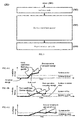
- FIG. 4 shows illustrations of available energy versus time of example scenarios for available stored energy in energy harvesting systems having a known implementation of load circuits such as that shown in FIG. 2 .
- the dashed lines show the amount of harvested energy (without consumption by the boot operation); the solid lines show the amount of consumed energy.
- FIG. 4(a) shows how the available energy increases in good harvesting conditions where the harvested energy substantively exceeds the energy consumed by the system. Consequently, the boot operation can proceed uninterrupted.
- FIG. 4(b) illustrates one potential problem that could occur in poor harvesting conditions, as described above. In this case, the power harvesting occurs at a lower rate, so the stored energy increases more slowly with time.
- FIG. 4(c) shows how a system might in some scenarios thrash between a reset state and a non-reset state when the energy cost of executing the boot sequence is large compared to the replenishing harvested energy. This could potentially prevent the system from completing the boot sequence for prolonged periods of time.
- FIG. 5 shows an illustration of available energy versus time of the available stored energy during harvesting operation during poor energy harvesting conditions, according to an embodiment. More specifically, FIG. 5 , shows an illustration of available energy versus time for a system having a modified boot operation (e.g., by interrupting, pausing, or changing the boot process), according to an embodiment.
- the boot operation can be modified, for example, based on information about the harvesting conditions such that the energy consumption of the boot process is reduced, allowing the harvested power to exceed the consumed power.
- the stored energy does not decrease so far that it prevents the boot operation from completing successfully, in contrast to FIGS.
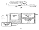
- FIG. 6 shows a block diagram of a subsystem that uses information about the power harvesting conditions to alter a reset or boot operation, according to an embodiment.
- subsystem 600 of FIG. 6 represents an implementation of load circuits (such as load circuits 140 in FIG. 1 ), according to an embodiment.
- reset signal 601 can correspond to the voltage V DD (s) 133 supplied by DC-DC regulator 130 to the load circuits 140.
- the subsystem 600 includes a processor 602 connected or operably coupled to non-volatile memory 603 and volatile memory 604.
- Processor 602 can be similar to the processor 210 of FIG. 2
- non-volatile memory 603 and volatile memory 604 can be similar to the non-volatile memory 220 and volatile 230, respectively, of FIG. 2 .
- the subsystem of FIG. 6 also includes a boot override component, which is connected or operatively coupled to processor 602, non-volatile memory 602 and/or volatile memory 604.
- the reset signal 601 is received by processor 602 and boot override component 610.
- Boot override component 610 also receives power and energy parameters 611.
- the boot override component 610 receives as inputs the existing reset signal(s) and parameters related to the power and energy harvesting conditions.
- the boot override component 610 determines information about the power harvesting, energy harvesting, and energy storage conditions for the system (e.g., the integrated circuit or the system on chip) and uses that information to alter the reset or boot sequence execution.
- the boot override component 610 can be, for example, a component or module within the subsystem 600 or outside of the subsystem 600, and operatively coupled to the processor 602, non-volatile memory 603 and/or volatile memory 604.
- the boot override component 600 can be a component or module within the processor 602, non-volatile memory 603 and/or volatile memory 604.
- the boot override component 610 can be in the form of hardware, firmware or software (stored in memory or executing in hardware / firmware) including for example a block of hardware / firmware or an extra line of code or subroutine of software / firmware stored in memory or executing in hardware.
- the power and energy parameters 611 received by and/or the power harvesting conditions computed by the boot override component 610 can include, for example, the state of the system's available energy stored in the energy storage element (e.g., energy storage element 120 in FIG. 1 ), the power or energy used to perform different portions of the boot process, the value of supply voltage rails in the system (e.g., voltage V DD (s) 133 in FIG. 1 ), the current drawn by supply voltage rails in the system (e.g., current I VDD 134 in FIG. 1 ), various derivatives of current drawn by supply voltage rails in the system (e.g., current I VDD 134 in FIG.
- the value of the voltage on the energy storage node e.g., voltage V CAP 121 in FIG. 1
- various derivatives of the voltage on the energy storage node e.g., voltage V CAP 121 in FIG. 1
- the current delivered to the energy storage node e.g., current I CAP 122 in FIG. 1
- various derivatives of the current delivered to the energy storage node e.g., current I CAP 122 in FIG. 1
- the current drawn from the energy storage node e.g., current I LOAD 132 in FIG. 1
- various derivatives of the current drawn from the energy storage node e.g., current I LOAD 132 in FIG.
- the input voltage to the energy harvesting circuit 111 various derivatives of the input voltage to the energy harvesting circuit (e.g., voltage V IN 111 in FIG. 1 ), the input current to the energy harvesting circuit (e.g., current I IN 112 in FIG. 1 ), various derivatives of the input current to the energy harvesting circuit (e.g., current I IN 112 in FIG. 1 ), the harvested power from the energy harvest circuit (e.g., power P H (t) 113 in FIG. 1 ), the current delivered from the energy harvesting circuit (e.g., current I H 114 in FIG. 1 ), various derivatives of the current delivered from the energy harvesting circuit (e.g., current I H 114 in FIG.
- the load power e.g., load power P LOAD (t) 131 in FIG. 1
- outputs from a built-in self-test not shown
- values stored in memory related to prior power transitions e.g., values stored in memories 220 and/or 230 in FIG. 2
- previous or current states of the energy harvesting circuits e.g., energy harvesting circuit 110 in FIG. 1
- type of power source e.g., energy harvesting circuit vs. battery / energy storage element vs. universal serial bus (USB) (not shown)
- the boot override component 610 and/or some other component (now shown) acting on the components within the subsystem 600 may intervene, oversee, stall, interrupt, stop, or re-direct the normal boot process or boot sequence.
- the output of the boot override component 610 can cause a change / modification in the boot sequence such that the processor executes the modified boot sequence in response to a boot request.
- this change / modification in the boot sequence will effectively reduce the current drawn by the load circuits (e.g., current I LOAD 132 in FIG. 1 ), thereby conserving energy on the energy storage element (e.g., energy storage element 120 in FIG.
- This may include performing an action to alter the peak load current (e.g., current I LOAD 132 in FIG. 1 ), the average load current (e.g., current I LOAD 132 in FIG. 1 ), the power drawn by the load (e.g., load power P LOAD (t) 131 in FIG. 1 ), or the energy consumed by the load (e.g., the energy consumed by load circuits 140 in FIG. 1 ).
- the peak load current e.g., current I LOAD 132 in FIG. 1
- the average load current e.g., current I LOAD 132 in FIG. 1
- the power drawn by the load e.g., load power P LOAD (t) 131 in FIG. 1
- the energy consumed by the load e.g., the energy consumed by load circuits 140 in FIG. 1 ).
- the following discussion provides several examples of the actions that can be performed in response to an instruction (or control signal) sent by the boot override component 610, for example, based on power harvesting conditions associated with an energy harvesting circuit and/or energy storage element (such as the energy harvesting circuit 110 and/or energy storage element 120 of FIG. 1 ).
- the action performed in response to the power harvesting conditions might make changes to the hardware (e.g., processor 602, non-volatile memory 603 and/or volatile memory 604).
- the action performed in response to the power harvesting conditions might make changes to the software (e.g., software executing on processor 602, and/or software stored in non-volatile memory 603 and/or volatile memory 604).
- the action performed in response to the power harvesting conditions might make changes to the boot loader options or to the boot mode (e.g., a boot sequence can be segmented and modified to define a set of modified boot sequence segments).
- the action performed in response to the power harvesting conditions might intercept the reset signal and only allow the reset to occur based on power harvesting conditions.
- the action performed in response to the power harvesting conditions might be to pause or stall at different points in normal boot sequence.
- the action performed in response to the power harvesting conditions might redefine the threshold for starting the boot sequence based on power conditions. For example, multiple thresholds may act as gating signals for subsets of the boot sequence.
- the action performed in response to the power harvesting conditions might modify the output or operation of a memory such as a non-volatile memory (e.g., the non-volatile memory 603 of FIG. 6 ).
- a memory such as a non-volatile memory (e.g., the non-volatile memory 603 of FIG. 6 ).
- This can be accomplished, for example, by defining a modified boot sequence such that a processor / IC executes the modified boot sequence in response to a boot request such that the operation of a memory is modified.
- the operation of a memory can be modified by pulling at least one pin to a level not determined by the non-volatile memory.
- the operation of the memory can be modified by modifying a level of at least one pin of the memory, independent of the operation of the memory.
- the output of the non-volatile memory might also be changed using a multiplexer (not shown) that replaces the output of the non-volatile memory with a different value.
- a multiplexer not shown
- These same techniques can be applied to boot code in volatile memory (e.g., volatile memory 604 of FIG. 6 ) as well.
- the action performed in response to the power harvesting conditions might be to interrupt or to preempt non-volatile memory access by loading boot code from a new location such as an external source, alternative memory, or different location in the on-chip memory.
- the action performed in response to the power harvesting conditions can be to interrupt, preempt or alter the non-volatile memory access by controlling the jump operand for a conditional jump(s) or controlling jump locations from the boot code.
- the control of the jump operand for a conditional jump(s) can be performed, for example, upon execution of a modified boot sequence.
- the control of the jump location can be implemented through a modified boot sequence.
- the action performed in response to the power harvesting conditions might be to alter the initialization of a peripheral component(s), for example by changing the memory-mapped locations associated with that peripheral component(s).
- the action performed in response to the power harvesting conditions can be to define alternative boot modes for peripheral blocks and to select the boot mode for a peripheral component(s) based on power conditions. For example, if normal operation would configure and enable a peripheral component(s), an alternative mode might configure but not enable the peripheral component(s).
- a peripheral component(s) is peripheral in the sense that it is located outside of and separate from the processor, IC or SoC that is performing the method(s) described herein.
- the action performed in response to the power harvesting conditions can change the behavior of the power management unit (PMU) on an SoC to alter its mode or state or control scheme.
- the boot override component can modify the operation of the PMU such that the operation associated with a memory is modified to define a modified boot sequence.
- the action performed in response to the power harvesting conditions can be to segment the boot sequence and to allow each segment of the boot sequence to execute depending on some combination of the energy consumed by the execution of that segment of the boot sequence and the available energy.
- the boot sequence can be divided into segments to define a set of boot sequence segments, and then the set of boot sequence segments can be modified to define a set of modified boot sequence segments.
- the set of modified boot sequence segments can be associated with timing information so that the timing of the execution of individual segments is controlled (e.g., a pause can be defined between the execution of adjacent segments).
- the set of modified boot sequence segments can be executed such that each boot sequence segment is executed at a time from a set of times.
- Each time from this set of times can be based on a threshold from a set of thresholds and for that segment and based on an amount of energy available at that time from the energy harvest circuit.
- the action performed in response to the power harvesting conditions can be to segment boot sequence and to re-order the execution of the segments of the boot sequence.
- the boot sequence can be divided into segments to define a set of boot sequence segments, and then the set of boot sequence segments can be modified to define a set of modified boot sequence segments by reordering at least two boot sequence segments.
- the action performed in response to the power harvesting conditions can be to define alternative boot programs or sub programs and to select the program or subprogram to run based on power conditions.
- a boot sequence can be divided into segments to define a set of boot sequence segments, and then the set of boot sequence segments can be modified to define a set of modified boot sequence segments by replacing at least one boot sequence segment with at least two alternative boot sequence segments, one of which will be executed depending on the power conditions.
- the action performed in response to the power harvesting conditions can be to stop operation of a segment of a boot sequence after it has already started, to roll back to a previous condition, and to re-start the operation, possibly in a delayed or modified state.
- the action performed in response to the power harvesting conditions can be control amount of data, rate of data, or pattern of data accessed in a memory (e.g., non-volatile memory 603 or volatile memory 604 of FIG. 6 ).
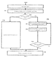
- FIG. 7 shows a flow diagram for the operation of a system that uses information about the power harvesting conditions to alter the reset or boot operation. Similar to the discussion above in connection with FIG. 3 , FIG. 7 refers to a process after exiting reset (or exiting a reset mode) by an electronic system having a processor (or IC) that is powering up for the first time or from a state without power (also referred to as a "cold start").
- the processor can involve altering the reset or boot operation, for example, by a pre-empting or preventing the boot process itself (e.g., pre-empting, preventing, or modifying the boot sequence of instructions).
- analog circuits may operate before the processor / IC has booted such that the analog circuits cause an alteration or modification to the boot sequence and the processor / IC executes this modified boot sequence upon power up or initial operational.
- This is in contrast to known systems have perform conventional power management techniques after the processor / IC has booted (e.g., after executing the boot sequence of instructions).
- this altered methodology makes a decision 702 about whether the normal boot process can proceed based in part on an assessment of power harvesting conditions 701. If so, then the normal boot process executes 710. If not, then an altered boot process executes 720, in which additional decisions are made to adjust the boot process based on power harvesting conditions until it completes.
- the altered boot process 720 includes assessing available power, energy conditions and boot state at 721, executing partial or modified boot process at 722, and determine whether the boot operation is done at 723. If the boot operation is done at 723, then execution of the user code is started at 730. If the boot operation is not done at 723, then the altered boot process 720 repeats starting at 721.
- the process of FIG. 7 can be applied to an energy harvesting wireless sensor having an energy harvesting and power management block (e.g., energy harvesting circuit 110, energy storage element 120, and/or DC-DC regulator 130 in FIG. 1 ), a processor, and a radio (e.g., the processor and radio collectively be represented by load circuits 140 in FIG. 1 ).
- a boot override component e.g., boot override component 610 of FIG. 6
- a boot override component can assess the power harvesting conditions and determine at 702 if a normal boot can occur, for example, by comparing the available stored energy and rate of incoming power to the computed energy consumption required to boot. If the available energy is higher, then a normal boot process occurs at 710. Otherwise, the boot override component causes the altered boot process at 720 to be performed. For example, the altered boot process can replace the jump locations of code emerging from the non-volatile memory for different subroutines in the boot process based on an ongoing assessment of available energy at 721.
- an electrical component is intended to mean a single electrical component or a combination of electrical components.
Landscapes
- Engineering & Computer Science (AREA)
- Theoretical Computer Science (AREA)
- General Engineering & Computer Science (AREA)
- General Physics & Mathematics (AREA)
- Physics & Mathematics (AREA)
- Software Systems (AREA)
- Human Computer Interaction (AREA)
- Computer Hardware Design (AREA)
- Computer Security & Cryptography (AREA)
- Computing Systems (AREA)
- Microelectronics & Electronic Packaging (AREA)
- Power Engineering (AREA)
- Power Sources (AREA)
- Stored Programmes (AREA)
Applications Claiming Priority (2)
| Application Number | Priority Date | Filing Date | Title |
|---|---|---|---|
| US14/679,748 US9292301B1 (en) | 2015-04-06 | 2015-04-06 | Systems, methods, and apparatus for controlling the power-on or boot sequence of an integrated circuit based on power harvesting conditions |
| US14/962,695 US9558008B2 (en) | 2015-04-06 | 2015-12-08 | Systems, methods, and apparatus for controlling the power-on or boot sequence of an integrated circuit based on power harvesting conditions |
Publications (1)
| Publication Number | Publication Date |
|---|---|
| EP3079036A1 true EP3079036A1 (de) | 2016-10-12 |
Family
ID=55754100
Family Applications (1)
| Application Number | Title | Priority Date | Filing Date |
|---|---|---|---|
| EP16163919.0A Withdrawn EP3079036A1 (de) | 2015-04-06 | 2016-04-05 | Systeme, verfahren und vorrichtung zur steuerung der einschalt- oder hochfahrsequenz einer integrierten schaltung auf basis von energiegewinnungsbedingungen |
Country Status (6)
| Country | Link |
|---|---|
| US (3) | US9558008B2 (de) |
| EP (1) | EP3079036A1 (de) |
| JP (1) | JP2016197410A (de) |
| KR (1) | KR20160119702A (de) |
| CN (1) | CN106055060A (de) |
| HK (1) | HK1225466A1 (de) |
Families Citing this family (8)
| Publication number | Priority date | Publication date | Assignee | Title |
|---|---|---|---|---|
| US9558008B2 (en) | 2015-04-06 | 2017-01-31 | Psikick, Inc | Systems, methods, and apparatus for controlling the power-on or boot sequence of an integrated circuit based on power harvesting conditions |
| US9888337B1 (en) | 2015-07-25 | 2018-02-06 | Gary M. Zalewski | Wireless coded communication (WCC) devices with power harvesting power sources for WiFi communication |
| US9911290B1 (en) | 2015-07-25 | 2018-03-06 | Gary M. Zalewski | Wireless coded communication (WCC) devices for tracking retail interactions with goods and association to user accounts |
| US10447053B2 (en) * | 2016-12-27 | 2019-10-15 | Panasonic Intellectual Property Management Co., Ltd. | Terminal |
| JP6796203B2 (ja) * | 2017-06-23 | 2020-12-02 | 日立オートモティブシステムズ株式会社 | 電子制御装置 |
| US10585671B2 (en) * | 2017-07-17 | 2020-03-10 | International Business Machines Corporation | Resource-based boot sequence |
| US11966748B2 (en) * | 2021-09-30 | 2024-04-23 | Ati Technologies Ulc | Dynamic boot configuration |
| US12554906B2 (en) * | 2021-12-30 | 2026-02-17 | Intel Corporation | Low latency and highly programmable interrupt controller unit |
Citations (2)
| Publication number | Priority date | Publication date | Assignee | Title |
|---|---|---|---|---|
| US20090267570A1 (en) * | 2008-04-28 | 2009-10-29 | Nokia Corporation | Apparatus for providing boot-up capability signals and associated methods |
| US20120072740A1 (en) * | 2010-09-16 | 2012-03-22 | National Tsing Hua University | Power Booting Sequence Control System and Control Method Thereof |
Family Cites Families (12)
| Publication number | Priority date | Publication date | Assignee | Title |
|---|---|---|---|---|
| US5018062A (en) | 1987-10-23 | 1991-05-21 | A.I. Architects, Inc. | Method and apparatus for overriding a ROM routine in response to a reset |
| US6202091B1 (en) | 1997-12-08 | 2001-03-13 | Nortel Networks Limited | Process and apparatus for initializing a computer from power up |
| TWI317905B (en) * | 2006-01-09 | 2009-12-01 | Wistron Corp | A method for executing booting process under a abnormal situation and a control chip for booting process |
| US7594104B2 (en) * | 2006-06-09 | 2009-09-22 | International Business Machines Corporation | System and method for masking a hardware boot sequence |
| CN105137144B (zh) * | 2009-04-16 | 2018-04-17 | 全景电力有限公司 | 用于功率管理的系统及在该系统中测量功率消耗的方法 |
| US20130054945A1 (en) | 2011-08-24 | 2013-02-28 | Microsoft Corporation | Adaptive sensing for early booting of devices |
| TWI442321B (zh) | 2011-09-23 | 2014-06-21 | Wistron Corp | 電子裝置開機加速方法以及相關之電子裝置 |
| US9274805B2 (en) | 2012-02-24 | 2016-03-01 | Qualcomm Incorporated | System and method for thermally aware device booting |
| CN103390898B (zh) * | 2013-07-08 | 2015-06-17 | 东南大学 | 基于瞬时序分量功率的动态无功补偿控制器 |
| KR102060430B1 (ko) | 2013-08-08 | 2020-02-11 | 삼성전자주식회사 | 웨이크-업 시간을 줄일 수 있는 시스템 온 칩. 애플리케이션 프로세서, 및 상기 시스템 온 칩을 포함하는 컴퓨터 시스템 |
| US9292301B1 (en) | 2015-04-06 | 2016-03-22 | Psikick, Inc. | Systems, methods, and apparatus for controlling the power-on or boot sequence of an integrated circuit based on power harvesting conditions |
| US9558008B2 (en) | 2015-04-06 | 2017-01-31 | Psikick, Inc | Systems, methods, and apparatus for controlling the power-on or boot sequence of an integrated circuit based on power harvesting conditions |
-
2015
- 2015-12-08 US US14/962,695 patent/US9558008B2/en active Active
-
2016
- 2016-04-01 JP JP2016074602A patent/JP2016197410A/ja active Pending
- 2016-04-01 KR KR1020160040282A patent/KR20160119702A/ko not_active Withdrawn
- 2016-04-05 CN CN201610206016.7A patent/CN106055060A/zh active Pending
- 2016-04-05 EP EP16163919.0A patent/EP3079036A1/de not_active Withdrawn
- 2016-07-29 US US15/224,184 patent/US9959126B2/en active Active
- 2016-12-01 HK HK16113768.5A patent/HK1225466A1/en unknown
-
2018
- 2018-04-16 US US15/954,317 patent/US10572266B2/en active Active
Patent Citations (2)
| Publication number | Priority date | Publication date | Assignee | Title |
|---|---|---|---|---|
| US20090267570A1 (en) * | 2008-04-28 | 2009-10-29 | Nokia Corporation | Apparatus for providing boot-up capability signals and associated methods |
| US20120072740A1 (en) * | 2010-09-16 | 2012-03-22 | National Tsing Hua University | Power Booting Sequence Control System and Control Method Thereof |
Also Published As
| Publication number | Publication date |
|---|---|
| JP2016197410A (ja) | 2016-11-24 |
| US20180232240A1 (en) | 2018-08-16 |
| CN106055060A (zh) | 2016-10-26 |
| KR20160119702A (ko) | 2016-10-14 |
| US20160291983A1 (en) | 2016-10-06 |
| US9959126B2 (en) | 2018-05-01 |
| US20160334852A1 (en) | 2016-11-17 |
| US9558008B2 (en) | 2017-01-31 |
| US10572266B2 (en) | 2020-02-25 |
| HK1225466A1 (en) | 2017-09-08 |
Similar Documents
| Publication | Publication Date | Title |
|---|---|---|
| US10572266B2 (en) | Systems, methods, and apparatus for controlling the power-on or boot sequence of an integrated circuit based on power harvesting conditions | |
| US12248355B2 (en) | System on chip for reducing wake-up time, method of operating same, and computer system including same | |
| US9563226B2 (en) | Dynamic clock regulation based on duty cycle thresholds | |
| US10383062B2 (en) | Power management integrated circuit, power management method, mobile device and clock adjusting method | |
| US9292301B1 (en) | Systems, methods, and apparatus for controlling the power-on or boot sequence of an integrated circuit based on power harvesting conditions | |
| US9612653B2 (en) | Integrated circuit with selectable power-on reset mode | |
| US9471140B2 (en) | Valid context status retention in processor power mode management | |
| US11119559B2 (en) | Controlling a processor clock | |
| US20240370078A1 (en) | Robust platform low power mode via embedded controller-based health policy to correct anomalous computer idle conditions | |
| EP2804285B1 (de) | Leistungsarbitrierungsverfahren und Vorrichtung mit einer Steuerlogikschaltung zur Bewertung und Auswahl von Stromversorgung | |
| JP6908664B2 (ja) | 電源ユニットホールドアップ時間を延長するためのシステムおよび方法 | |
| US10496298B2 (en) | Configurable flush of data from volatile memory to non-volatile memory | |
| US10915257B2 (en) | Semiconductor device and semiconductor system | |
| US7765412B1 (en) | Methods and systems for dynamically changing device operating conditions | |
| KR20150006320A (ko) | 반도체 집적 회로 및 반도체 집적 회로의 동작 방법 |
Legal Events
| Date | Code | Title | Description |
|---|---|---|---|
| PUAI | Public reference made under article 153(3) epc to a published international application that has entered the european phase |
Free format text: ORIGINAL CODE: 0009012 |
|
| AK | Designated contracting states |
Kind code of ref document: A1 Designated state(s): AL AT BE BG CH CY CZ DE DK EE ES FI FR GB GR HR HU IE IS IT LI LT LU LV MC MK MT NL NO PL PT RO RS SE SI SK SM TR |
|
| AX | Request for extension of the european patent |
Extension state: BA ME |
|
| STAA | Information on the status of an ep patent application or granted ep patent |
Free format text: STATUS: REQUEST FOR EXAMINATION WAS MADE |
|
| 17P | Request for examination filed |
Effective date: 20170407 |
|
| RBV | Designated contracting states (corrected) |
Designated state(s): AL AT BE BG CH CY CZ DE DK EE ES FI FR GB GR HR HU IE IS IT LI LT LU LV MC MK MT NL NO PL PT RO RS SE SI SK SM TR |
|
| REG | Reference to a national code |
Ref country code: HK Ref legal event code: DE Ref document number: 1225466 Country of ref document: HK |
|
| STAA | Information on the status of an ep patent application or granted ep patent |
Free format text: STATUS: EXAMINATION IS IN PROGRESS |
|
| 17Q | First examination report despatched |
Effective date: 20180320 |
|
| STAA | Information on the status of an ep patent application or granted ep patent |
Free format text: STATUS: THE APPLICATION HAS BEEN WITHDRAWN |
|
| 18W | Application withdrawn |
Effective date: 20180830 |
|
| REG | Reference to a national code |
Ref country code: HK Ref legal event code: WD Ref document number: 1225466 Country of ref document: HK |