EP3078903B1 - Lighting module - Google Patents
Lighting module Download PDFInfo
- Publication number
- EP3078903B1 EP3078903B1 EP16165828.1A EP16165828A EP3078903B1 EP 3078903 B1 EP3078903 B1 EP 3078903B1 EP 16165828 A EP16165828 A EP 16165828A EP 3078903 B1 EP3078903 B1 EP 3078903B1
- Authority
- EP
- European Patent Office
- Prior art keywords
- frame
- fluorescent material
- led chip
- disposed
- light
- Prior art date
- Legal status (The legal status is an assumption and is not a legal conclusion. Google has not performed a legal analysis and makes no representation as to the accuracy of the status listed.)
- Active
Links
- 239000000463 material Substances 0.000 claims description 177
- 230000003287 optical effect Effects 0.000 claims description 94
- 239000000758 substrate Substances 0.000 claims description 64
- 229920005989 resin Polymers 0.000 claims description 40
- 239000011347 resin Substances 0.000 claims description 40
- 108010043121 Green Fluorescent Proteins Proteins 0.000 claims description 22
- 238000009877 rendering Methods 0.000 description 9
- 238000001228 spectrum Methods 0.000 description 8
- BPQQTUXANYXVAA-UHFFFAOYSA-N Orthosilicate Chemical compound [O-][Si]([O-])([O-])[O-] BPQQTUXANYXVAA-UHFFFAOYSA-N 0.000 description 6
- 230000000875 corresponding effect Effects 0.000 description 6
- 235000019592 roughness Nutrition 0.000 description 5
- 229920003002 synthetic resin Polymers 0.000 description 5
- 239000000057 synthetic resin Substances 0.000 description 5
- 238000010168 coupling process Methods 0.000 description 4
- 230000004907 flux Effects 0.000 description 4
- 150000004767 nitrides Chemical class 0.000 description 4
- 230000001276 controlling effect Effects 0.000 description 3
- 230000000694 effects Effects 0.000 description 3
- 239000002245 particle Substances 0.000 description 3
- 230000005855 radiation Effects 0.000 description 3
- 229910003564 SiAlON Inorganic materials 0.000 description 2
- 238000005452 bending Methods 0.000 description 2
- 230000008901 benefit Effects 0.000 description 2
- 238000009792 diffusion process Methods 0.000 description 2
- 239000002223 garnet Substances 0.000 description 2
- 229910052909 inorganic silicate Inorganic materials 0.000 description 2
- UCKMPCXJQFINFW-UHFFFAOYSA-N Sulphide Chemical compound [S-2] UCKMPCXJQFINFW-UHFFFAOYSA-N 0.000 description 1
- 239000000956 alloy Substances 0.000 description 1
- 229910045601 alloy Inorganic materials 0.000 description 1
- 239000000919 ceramic Substances 0.000 description 1
- 238000006243 chemical reaction Methods 0.000 description 1
- 230000002596 correlated effect Effects 0.000 description 1
- 230000003247 decreasing effect Effects 0.000 description 1
- 230000002996 emotional effect Effects 0.000 description 1
- 239000003822 epoxy resin Substances 0.000 description 1
- 230000005284 excitation Effects 0.000 description 1
- 230000005484 gravity Effects 0.000 description 1
- 239000002184 metal Substances 0.000 description 1
- 229910052751 metal Inorganic materials 0.000 description 1
- 238000000034 method Methods 0.000 description 1
- 239000000203 mixture Substances 0.000 description 1
- 230000004048 modification Effects 0.000 description 1
- 238000012986 modification Methods 0.000 description 1
- 229920000647 polyepoxide Polymers 0.000 description 1
- 230000008569 process Effects 0.000 description 1
- 230000004044 response Effects 0.000 description 1
- 229920002050 silicone resin Polymers 0.000 description 1
Images


Classifications
-
- F—MECHANICAL ENGINEERING; LIGHTING; HEATING; WEAPONS; BLASTING
- F21—LIGHTING
- F21K—NON-ELECTRIC LIGHT SOURCES USING LUMINESCENCE; LIGHT SOURCES USING ELECTROCHEMILUMINESCENCE; LIGHT SOURCES USING CHARGES OF COMBUSTIBLE MATERIAL; LIGHT SOURCES USING SEMICONDUCTOR DEVICES AS LIGHT-GENERATING ELEMENTS; LIGHT SOURCES NOT OTHERWISE PROVIDED FOR
- F21K9/00—Light sources using semiconductor devices as light-generating elements, e.g. using light-emitting diodes [LED] or lasers
- F21K9/60—Optical arrangements integrated in the light source, e.g. for improving the colour rendering index or the light extraction
-
- F—MECHANICAL ENGINEERING; LIGHTING; HEATING; WEAPONS; BLASTING
- F21—LIGHTING
- F21V—FUNCTIONAL FEATURES OR DETAILS OF LIGHTING DEVICES OR SYSTEMS THEREOF; STRUCTURAL COMBINATIONS OF LIGHTING DEVICES WITH OTHER ARTICLES, NOT OTHERWISE PROVIDED FOR
- F21V7/00—Reflectors for light sources
- F21V7/0008—Reflectors for light sources providing for indirect lighting
-
- F—MECHANICAL ENGINEERING; LIGHTING; HEATING; WEAPONS; BLASTING
- F21—LIGHTING
- F21V—FUNCTIONAL FEATURES OR DETAILS OF LIGHTING DEVICES OR SYSTEMS THEREOF; STRUCTURAL COMBINATIONS OF LIGHTING DEVICES WITH OTHER ARTICLES, NOT OTHERWISE PROVIDED FOR
- F21V7/00—Reflectors for light sources
- F21V7/005—Reflectors for light sources with an elongated shape to cooperate with linear light sources
-
- F—MECHANICAL ENGINEERING; LIGHTING; HEATING; WEAPONS; BLASTING
- F21—LIGHTING
- F21V—FUNCTIONAL FEATURES OR DETAILS OF LIGHTING DEVICES OR SYSTEMS THEREOF; STRUCTURAL COMBINATIONS OF LIGHTING DEVICES WITH OTHER ARTICLES, NOT OTHERWISE PROVIDED FOR
- F21V7/00—Reflectors for light sources
- F21V7/04—Optical design
- F21V7/06—Optical design with parabolic curvature
-
- F—MECHANICAL ENGINEERING; LIGHTING; HEATING; WEAPONS; BLASTING
- F21—LIGHTING
- F21V—FUNCTIONAL FEATURES OR DETAILS OF LIGHTING DEVICES OR SYSTEMS THEREOF; STRUCTURAL COMBINATIONS OF LIGHTING DEVICES WITH OTHER ARTICLES, NOT OTHERWISE PROVIDED FOR
- F21V7/00—Reflectors for light sources
- F21V7/04—Optical design
- F21V7/07—Optical design with hyperbolic curvature
-
- F—MECHANICAL ENGINEERING; LIGHTING; HEATING; WEAPONS; BLASTING
- F21—LIGHTING
- F21V—FUNCTIONAL FEATURES OR DETAILS OF LIGHTING DEVICES OR SYSTEMS THEREOF; STRUCTURAL COMBINATIONS OF LIGHTING DEVICES WITH OTHER ARTICLES, NOT OTHERWISE PROVIDED FOR
- F21V7/00—Reflectors for light sources
- F21V7/04—Optical design
- F21V7/08—Optical design with elliptical curvature
-
- F—MECHANICAL ENGINEERING; LIGHTING; HEATING; WEAPONS; BLASTING
- F21—LIGHTING
- F21Y—INDEXING SCHEME ASSOCIATED WITH SUBCLASSES F21K, F21L, F21S and F21V, RELATING TO THE FORM OR THE KIND OF THE LIGHT SOURCES OR OF THE COLOUR OF THE LIGHT EMITTED
- F21Y2103/00—Elongate light sources, e.g. fluorescent tubes
- F21Y2103/10—Elongate light sources, e.g. fluorescent tubes comprising a linear array of point-like light-generating elements
-
- F—MECHANICAL ENGINEERING; LIGHTING; HEATING; WEAPONS; BLASTING
- F21—LIGHTING
- F21Y—INDEXING SCHEME ASSOCIATED WITH SUBCLASSES F21K, F21L, F21S and F21V, RELATING TO THE FORM OR THE KIND OF THE LIGHT SOURCES OR OF THE COLOUR OF THE LIGHT EMITTED
- F21Y2115/00—Light-generating elements of semiconductor light sources
- F21Y2115/10—Light-emitting diodes [LED]
-
- H—ELECTRICITY
- H01—ELECTRIC ELEMENTS
- H01L—SEMICONDUCTOR DEVICES NOT COVERED BY CLASS H10
- H01L33/00—Semiconductor devices with at least one potential-jump barrier or surface barrier specially adapted for light emission; Processes or apparatus specially adapted for the manufacture or treatment thereof or of parts thereof; Details thereof
- H01L33/48—Semiconductor devices with at least one potential-jump barrier or surface barrier specially adapted for light emission; Processes or apparatus specially adapted for the manufacture or treatment thereof or of parts thereof; Details thereof characterised by the semiconductor body packages
- H01L33/50—Wavelength conversion elements
- H01L33/501—Wavelength conversion elements characterised by the materials, e.g. binder
- H01L33/502—Wavelength conversion materials
- H01L33/504—Elements with two or more wavelength conversion materials
Definitions
- Embodiments relate to a lighting module.
- an electric bulb or a fluorescent lamp is commonly used as an indoor or outdoor lighting lamp.
- the electric bulb or the fluorescent lamp has a short life span, so that it should be frequently changed.
- a conventional fluorescent lamp is degraded due to elapse of time for its use. As a result, it is often that its illuminance is gradually decreased.
- LED a light emitting device
- US2006203512 A1 hereinafter, referred to as LED.
- the LED is easy to control and has a rapid response speed, high electro-optic conversion efficiency, a long life span, low power consumption and high luminance.
- the LED is also used to create emotional lighting.
- the objective of the present invention is to provide a lighting module which does not use a light guide plate.
- the objective of the present invention is to provide a lighting module capable of controlling light distribution.
- the objective of the present invention is to provide a lighting module of which the lamp apparatus efficiency is higher than 80 % and the height (thickness) is less than 20 mm.
- the objective of the present invention is to provide a lighting module including a light source which has a high color rendering property.
- the objective of the present invention is to provide a lighting module including a light source which has high color reproductivity and excellent color uniformity.
- the lighting module comprises: an optical plate; a base frame including a central frame disposed on the optical plate, a first frame coupled to the central frame, and a second frame coupled to the first frame; a side frame coupled between the optical plate and the second frame of the base frame; and a light source including a substrate disposed on the side frame and a light emitter disposed on the substrate.
- the second frame is disposed on the light source.
- the second frame has an inner surface reflecting light from the light source to at least one of the first frame and the central frame.
- the cross sectional shape of the inner surface of the second frame is at least one of a parabolic shape, a hyperbolic shape and an elliptical shape.
- the thickness of the central frame is larger than that of the first frame.
- the thickness of the first frame becomes larger toward the central frame from the second frame.
- the thickness of the central frame becomes larger toward the center of the central frame from one side of the central frame.
- the inner surface of the first frame becomes closer to the optical plate toward the central frame from the second frame.
- the inner surface of the central frame becomes closer to the optical plate toward the center of the central frame from one side of the central frame.
- the side frame comprises a coupler which is coupled to one side of the optical plate.
- the light emitter of the light source comprises: a first light emitter disposed on the substrate; and a second light emitter disposed on the substrate and around the first light emitter.
- the first light emitter comprises a red LED chip, a green LED chip and a first blue LED chip.
- the second light emitter comprises a second blue LED chip having a wavelength of from 470 nm to 490 nm; and a yellow fluorescent material disposed around the second blue LED chip.
- the second light emitter comprises: a first fluorescent material film which is disposed on the second blue LED chip and comprises the yellow fluorescent material; a resin packer which is disposed on the first fluorescent material film; and a second fluorescent material film which is disposed on the resin packer and comprises the yellow fluorescent material.
- the first light emitter further comprises a first body in which the red LED chip, the green LED chip and the first blue LED chip are disposed.
- the second light emitter further comprises a second body in which the second blue LED chip and the yellow fluorescent material are disposed.
- the light emitter of the light source comprises: a first light emitter disposed on the substrate; and a second light emitter disposed on the substrate and around the first light emitter.
- the first light emitter comprises a red LED chip, a green LED chip and a first blue LED chip.
- the second light emitter comprises a second blue LED chip having a wavelength of from 470 nm to 490 nm; and at least one of a red fluorescent material and a green fluorescent material which are disposed around the second blue LED chip.
- the second light emitter comprises: a first fluorescent material film which is disposed on the second blue LED chip and comprises any one of the red fluorescent material and the green fluorescent material; a resin packer which is disposed on the first fluorescent material film; and a second fluorescent material film which is disposed on the resin packer and comprises any one of the red fluorescent material and the green fluorescent material.
- the first light emitter further comprises a first body in which the red LED chip, the green LED chip and the first blue LED chip are disposed.
- the second light emitter further comprises a second body in which the second blue LED chip and any one of the red fluorescent material and the green fluorescent material are disposed.
- the lighting module comprises: an optical plate; a base frame including a central frame disposed on the optical plate, a first frame coupled to the central frame, and a second frame coupled to the first frame; a side frame coupled between the optical plate and the second frame of the base frame; and a light source including a substrate disposed on the side frame in such a manner as to be perpendicular to the optical plate, and a light emitter disposed on the substrate.
- the side frame comprises: a first side frame on which the substrate of the light source is disposed and which is coupled to the second frame of the base frame; and a second side frame which is coupled to the first side frame and is coupled to optical plate.
- the second frame of the base frame has a recess receiving one side of the substrate of the light source.
- the second side frame of the side frame has a recess receiving the other side of the substrate of the light source.
- the second side frame of the side frame comprises a coupler which is coupled to a portion of the optical plate.
- the thickness of the first frame of the base frame is uniform.
- the thickness of the central frame is larger than that of the first frame.
- the inner surface of the first frame comprises a predetermined roughness.
- the cross sectional shape of the central frame of the base frame is a hemisphere or a semi-ellipse.
- a lighting module according to the embodiment does not use a light guide plate, thereby causing the lighting module to be lighter and to have a low unit cost.
- a lighting module according to the embodiment is capable of controlling light distribution.
- a lighting module according to the embodiment has a lamp apparatus efficiency higher than 80 % and height (thickness) less than 20 mm
- a lighting module according to the embodiment is capable of providing white light having a high color rendering property by creating a full spectrum based on wavelengths.
- a lighting module according to the embodiment is capable of providing high color reproductivity and excellent color uniformity.
- each layer is magnified, omitted or schematically shown for the purpose of convenience and clearness of description.
- the size of each component does not necessarily mean its actual size.
- an element when it is mentioned that an element is formed “on” or “under” another element, it means that the mention includes a case where two elements are formed directly contacting with each other or are formed such that at least one separate element is interposed between the two elements.
- the "on” and “under” will be described to include the upward and downward directions based on one element.
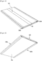
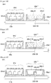
- Fig. 1 is a top perspective view of a lighting module according to a first embodiment.
- Fig. 2 is a bottom perspective view of the lighting module shown in Fig. 1 .
- Fig. 3 is an exploded perspective view of the lighting module shown in Fig. 2 .
- Fig. 4 is a cross sectional view of the lighting module shown in Fig. 1 .
- the lighting module according to the first embodiment may comprise a base frame 100, side frames 300a and 300b, light sources 500a and 500b, and an optical plate 700.
- the base frame 100 may have a plate shape having an outer surface and an inner surface.
- the outer surface of the base frame 100 forms the appearance of the lighting module according to the embodiment.
- the inner surface of the base frame 100 is disposed within the lighting module according to the embodiment and reflects light from the light sources 500a and 500b to the optical plate 700.
- the base frame 100 may comprise a plurality of frames. Specifically, the base frame 100 may comprise a central frame 110, first frames 130a and 130b, and second frames 150a and 150b.
- the central frame 110 is disposed at the center of the base frame 100.
- the central frame 110 reflects the light from the light sources 500a and 500b to the optical plate 700.
- an inner surface of the central frame 110 may project outwardly or may be convex.
- the inner surface of the central frame 110 becomes closer to the optical plate 700 toward the center of the central frame 110 from both sides of the central frame 110.
- the central frame 110 becomes thicker toward the center of the central frame 110 from both sides of the central frame 110.
- the first frames 130a and 130b comprise a first side first frame 130a and a second side first frame 130b.
- One side of the first side first frame 130a is coupled to one side of both sides of the central frame 110.
- One side of the second side first frame 130b is coupled to the other side of both sides of the central frame 110.
- the first frames 130a and 130b and the central frame 110 may be integrally formed with each other.
- the first side first frame 130a may become thicker toward the central frame 110 from the second frame 150a. Contrarily, the first side first frame 130a may become thinner toward the second frame 150a from the central frame 110. Also, an inner surface of the first side first frame 130a becomes closer to the optical plate 700 toward the central frame 110 from the second frame 150a. Contrarily, the inner surface of the first side first frame 130a becomes farther from the optical plate 700 toward the second frame 150a from the central frame 110.
- the central frame 110 is thicker than the first frame 130a. Also, a distance from the inner surface of the central frame 110 to the optical plate 700 is less than a distance from the inner surface of the first frame 130a to the optical plate 700.
- the inner surface of the first side first frame 130a may reflect light, which is directly or indirectly incident from the first light source 500a, to the central frame 110 and the optical plate 700.
- An inner surface of the second side first frame 130b may reflect light, which is directly or indirectly incident from the second light source 500b, to the central frame 110 and the optical plate 700.
- the second frames 150a and 150b comprise a first side second frame 150a and a second side second frame 150b.
- the first side second frame 150a is coupled to the other side of the first side first frame 130a.
- the second side second frame 150b is coupled to the other side of the second side first frame 130b.
- the second frames 150a and 150b may be integrally formed with the first frames 130a and 130b or may be integrally formed with the first frames 130a and 130b and the central frame 110.
- An inner surface of the first side second frame 150a reflects the light from the first light source 500a to the first side first frame 130a, the central frame 110 and the optical plate 700.
- An inner surface of the second side second frame 150b reflects the light from the second light source 500b to the second side first frame 130b, the central frame 110 and the optical plate 700.
- the inner surfaces of the second frames 150a and 150b may have various shapes. Specifically, the inner surfaces of the second frames 150a and 150b may have any one of a parabolic shape, a hyperbolic shape and an elliptical shape. This will be described with reference to Figs. 5 to 7 .
- Fig. 5 is a view for describing a traveling path of light when an inner surface of a second frame shown in Fig. 4 has a parabolic shape.
- the inner surfaces of the second frames 150a and 150b have a parabolic shape.
- the inner surfaces of the second frames 150a and 150b reflect the light incident from the light emitting devices 530a and 530b in parallel with the optical plate 700. Therefore, the light reflected by the inner surfaces of the second frames 150a and 150b may be incident on the inner surfaces of the first frames 130a and 130b and the central frame 110.
- the second frames 150a and 150b having the parabolic inner surface have an advantage to collect a large amount of the light to the inner surface of the central frame 110.
- Fig. 6 is a view for describing a traveling path of light when the inner surface of a second frame shown in Fig. 4 has a hyperbolic shape.
- the inner surfaces of the second frames 150a and 150b have a hyperbolic shape.
- the inner surfaces of the second frames 150a and 150b diffuse the light incident from the light emitting devices 530a and 530b. Therefore, the light reflected by the inner surfaces of the second frames 150a and 150b may be incident more on the inner surfaces of the first frames 130a and 130b, particularly, on the first frames 130a and 130b adjacent to the second frames 150a and 150b.
- Fig. 7 is a view for describing a traveling path of light when the inner surface of a second frame shown in Fig. 4 has an elliptical shape.
- the inner surfaces of the second frames 150a and 150b have an elliptical shape.
- the inner surfaces of the second frames 150a and 150b collect the light incident from the light emitting devices 530a and 530b to the other focus of the ellipse. Therefore, most of the light reflected by the inner surfaces of the second frames 150a and 150b may be incident on the inner surfaces of the first frames 130a and 130b, particularly, on the central frame 110.
- the side frames 300a and 300b are disposed on both side of the central base 110 respectively.
- the side frames 300a and 300b may comprise a first side frame 300a and a second side frame 300b.
- the first side frame 300a may be coupled to the first side second frame 150a of the base frame 100.
- the second side frame 300b may be coupled to the second side second frame 150b of the base frame 100.
- the first side frame 300a and the second side frame 300b support both sides of the base frame 100 and both sides of the optical plate 700, so that the base frame 100 and the optical plate 700 can be spaced apart from each other.
- the first side frame 300a and the second side frame 300b receive the first light source 500a and the second light source 500b. Specifically, the first side frame 300a receives the first light source 500a. The second side frame 300b receives the second light source 500b.
- the first side frame 300a is coupled to the first side second frame 150a of the base frame 100 and is coupled to one side of the optical plate 700.
- the second side frame 300b is coupled to the second side second frame 150b of the base frame 100 and is coupled to the other side of the optical plate 700.
- the first side frame 300a may comprise a first_A side frame 310a and a second_A side frame 330a.
- the first_A side frame 310a is coupled to the base frame 100.
- the second_A side frame 330a is coupled to one side of the optical plate 700.
- the first_A side frame 310a and the second_A side frame 330a may have a plate shape respectively and may form a predetermined angle.
- the first_A side frame 310a and the second_A side frame 330a may be formed in correspondence with the shapes of the second frames 150a and 150b.
- the first_A side frame 310a and the second_A side frame 330a may be substantially perpendicular to each other.
- the first_A side frame 310a and the second_A side frame 330a may be integrally formed with each other and they can be distinguished as the first_A side frame 310a and the second_A side frame 330a by bending the first side frame 300a.
- An inner surface of the first_A side frame 310a may come in surface contact with and may be coupled to an outer surface of the first side second frame 150a of the base frame 100. Through the surface contact, heat radiated from the first light source 500a can be transferred to the base frame 100.
- the second_A side frame 330a is coupled to one side of the optical plate 700.
- the second_A side frame 330a may have a structure capable of receiving the one side of the optical plate 700.
- the second_A side frame 330a may have a coupler 335a allowing the second_A side frame 330a to be coupled to the one side of the optical plate 700. Thanks to the coupler 335a, the optical plate 700 can be coupled to the second_A side frame 330a in a sliding manner.
- the first light source 500a is disposed in the second_A side frame 330a.
- the first light source 500a disposed in the second_A side frame 330a emits light toward the base frame 100.
- the second_A side frame 330a may be disposed in parallel with the optical plate 700. When the second_A side frame 330a is disposed in parallel with the optical plate 700, the position of the first light source 500a may be specified.
- the first side frame 300a and the second side frame 300b may be formed of a material capable of easily radiating the heat from the first light source 500a and the second light source 500b.
- the first side frame 300a and the second side frame 300b may be formed of Al, an alloy including Al, and the like.
- the base frame 100 may be also formed of the same heat radiating material as those of the first side frame 300a and the second side frame 300b. However, there is no limit to this.
- the base frame 100 may be formed of a material different from those of the first side frame 300a and the second side frame 300b.
- the light sources 500a and 500b may comprise the first light source 500a disposed in the first side frame 300a, and the second light source 500b disposed in the second side frame 300b.
- the second light source 500b is the same as the first light source 500a, a description of the second light source 500b will be replaced by the following description of the first light source 500a.
- the first light source 500a may comprise a substrate 510a and the light emitting device 530a.
- a plurality of the light emitting devices 530a may be disposed on one side of the substrate 510a in a row or may be disposed adjacent to each other.
- the other side of the substrate 510a is disposed in the second_A side frame 330a of the first side frame 300a.
- the substrate 510a and the optical plate 700 may be disposed on the same plane with each other. Otherwise, the substrate 510a may be disposed in parallel with the optical plate 700. Also, the substrate 510a may be disposed in parallel with the outer surface of the base frame 100.
- the substrate 510a may comprise a printed circuit board (PCB), a metal core PCB (MCPCB), a flexible PCB (FPCB), a ceramic substrate or the like.
- PCB printed circuit board
- MCPCB metal core PCB
- FPCB flexible PCB
- the light emitting device 530a may be a light emitting diode (LED).
- a position on which the light emitting device 530a is disposed on the substrate 510a may be changed according to the cross sectional shapes of the second frames 150a and 150b of the base frame 100. That is, when the cross sectional shapes of the second frames 150a and 150b are a parabolic shape, a hyperbolic shape and an elliptical shape, the light emitting device 530a may be disposed at a position corresponding to the foci of the parabola, hyperbola and ellipse. However, there is no limit to this. The light emitting device 530a may not be disposed at the position corresponding to the foci of the parabola, hyperbola and ellipse.
- the plurality of the light emitting devices 530a may emit the same colored light or differently colored lights.
- the light emitting device 530a may be a blue light emitting device or a white light emitting device having a high color rendering index (CRI).
- Synthetic resin including a fluorescent material is molded on a blue light emitting chip, so that the white light emitting device emits white light.
- the fluorescent material may comprise at least any one selected from a group consisting of a garnet material (YAG, TAG), a silicate material, a nitride material and an oxynitride material.
- natural light can be created by allowing the synthetic resin to comprise only yellow fluorescent material
- the synthetic resin may further comprise a green fluorescent material or a red fluorescent material in order to improve a color rendering index and to reduce a color temperature.
- an addition ratio of the color of the fluorescent material may be formed such that the green fluorescent material is more used than the red fluorescent material, and the yellow fluorescent material is more used than the green fluorescent material.
- the garnet material, the silicate material and the oxynitride material may be used as the yellow fluorescent material.
- the silicate material and the oxynitride material may be used as the green fluorescent material.
- the nitride material may be used as the red fluorescent material.
- the synthetic resin may be mixed with various kinds of the fluorescent materials or may be configured by a layer including the red fluorescent material, a layer including the green fluorescent material and a layer including the yellow fluorescent material, which are formed separately from each other.
- the first light source 500a may further comprise a heat radiation sheet (not shown).
- the heat radiation sheet (not shown) may be disposed between the substrate 510a and the first side frame 300a.
- the heat radiation sheet (not shown) may rapidly transfer the heat from the substrate 510a to the first side frame 300a.
- the light emitting devices 530a of the first light source 500a may have a color temperature different from that of the light emitting devices 530b of the second light source 500b.
- a plurality of the light emitting devices 530a comprised in the first light source 500a may be a warm white LED
- a plurality of the light emitting devices 530b comprised in the second light source 500b may be a cool white LED.
- the warm white LED and the cool white LED emit white light. Since the warm white LED and the cool white LED are able to emit mixed white light by emitting a correlated color temperature respectively, a color rendering index (CRI) representing how close light is to natural sunlight becomes larger. Accordingly, it is possible to prevent an actual color of an object from being distorted and to reduce fatigue of the eyes of a user.
- CRI color rendering index
- the optical plate 700 transmits the light which has been emitted from the light sources 500a and 500b and has been reflected by the inner surface of the base frame 100.
- the optical plate 700 may have a plate shape having an outer surface and an inner surface.
- the one side of the optical plate 700 may be coupled to the first side frame 300a.
- the other side of the optical plate 700 may be coupled to the second side frame 300b.
- the optical plate 700 may allow the light incident from the base frame 100 to pass therethrough as it is. Otherwise, the optical plate 700 may diffuse the light incident from the base frame 100.
- the optical plate 700 may comprise a diffusion material.
- the optical plate 700 may have a predetermined pattern for the purpose of more improving light diffusion rate.
- the pattern may have a concave lens shape or a convex lens shape.
- the optical plate 700 may be transparent, opaque or translucent.
- the optical plate 700 may emit light which is excited by the incident light and has a wavelength different from that of the incident light.
- the optical plate 700 may have a fluorescent material.
- the fluorescent material may comprise at least any one of a yellow fluorescent material, a green fluorescent material and a red fluorescent material.
- Fig. 8 is a graph showing an optical characteristic of the lighting module according to the first embodiment shown in Figs. 1 to 4 .
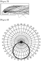
- Fig. 9 is a view showing a luminous flux distribution of the lighting module according to the first embodiment shown in Figs. 1 to 4 .
- uniformity, efficiency and a beam angle of the light emitted from the lighting module according to the first embodiment are about 83.3 %, about 87.2 % and about 110° respectively.
- a size of the lighting module according to the first embodiment shown in Figs. 1 to 4 may be reduced.
- the size and height of the lighting module according to the first embodiment may be within 300 ⁇ 600 (mm) and 20 mm respectively.
- Fig. 10 is a top perspective view of a lighting module according to a second embodiment.
- Fig. 11 is a bottom perspective view of the lighting module shown in Fig. 10 .
- Fig. 12 is an exploded perspective view of the lighting module shown in Fig. 11 .
- Fig. 13 is a cross sectional view of the lighting module shown in Fig. 10 .
- the lighting module according to the second embodiment comprises a base frame 100', side frame 300a' and 300b', light sources 500a' and 500b', and an optical plate 700.
- the optical plate 700 is the same as the optical plate 700 shown in Figs. 1 to 4 , a detailed description thereof will be omitted.
- the base frame 100' may comprise a central frame 110', first frames 130a' and 130b', and second frames 150a' and 150b'.
- a cross section of the central frame 110' may have a hemispherical shape.
- the hemispherical shape includes not only a geometrically perfect hemispherical shape but also a semi-elliptical shape.
- the first frames 130a' and 130b' comprise a first side first frame 130a' and a second side first frame 130b'.
- the first frames 130a' and 130b' may have a uniform thickness.
- Inner surfaces of the first frames 130a' and 130b' may have predetermined roughnesses 135a' and 135b'.
- the cross sectional shapes of the roughnesses 135a' and 135b' may be various, for example, a hemisphere, a semi-ellipse, a polygon or the like. Due to the roughnesses 135a' and 135b', light from the light sources 500a' and 500b' can be reflected toward the optical plate 700.
- the minimum thickness of the central frame 110' is larger than the thickness of the first frame 130a'.
- the minimum thickness of the central frame 110' may be the same as or larger than the thickness of the first frame 130a'.
- a distance from an inner surface of the central frame 110' to the optical plate 700 is less than a distance from the inner surface of the first frame 130a' to the optical plate 700.
- a distance from the thickest portion of the central frame 110' to the optical plate 700 may be less than the distance from the first frame 130a' to the optical plate 700.
- the second frames 150a' and 150b' comprise a first side second frame 150a' and a second side second frame 150b'.
- the first side second frame 150a' is coupled to the other side of the first side first frame 130a'.
- the second side second frame 150b' is coupled to the other side of the second side first frame 130b'.
- the second frames 150a' and 150b' may be integrally formed with the first frames 130a' and 130b' or may be integrally formed with the first frames 130a' and 130b' and the central frame 110'.
- An inner surface of the first side second frame 150a' may reflect the light from the first light source 500a' to the first side first frame 130a', the central frame 110' and the optical plate 700.
- An inner surface of the second side second frame 150b' may reflect the light from the second light source 500b' to the second side first frame 130b', the central frame 110' and the optical plate 700.
- the second frames 150a' and 150b' may have predetermined curved inner surfaces.
- the curved surface may have a curvature corresponding to an inner surface of a second_A side frame 330a'.
- the second frames 150a' and 150b' may have a recess 155a'.
- One sides of the light sources 500a' and 500b' may be disposed in the recess 155a'.
- the light sources 500a' and 500b' can be fixed by the recess 155a'.
- the recess 155a' and a recess 339a' of a first side frame 300a' receive both sides of substrates 510a' and 510b' of the light sources 500a' and 500b'.
- the substrates 510a' and 510b' may be coupled in a sliding manner via the recesses 155a' of the second frames 150a' and 150b' and via the recess 339a'of the first side frame 300a'.
- the coupling method of the substrates 510a' and 510b' is not limited to the sliding manner.
- the side frames 300a' and 300b' may comprise the first side frame 300a' and a second side frame 300b'.
- the first side frame 300a' may comprise a first_A side frame 310a' and a second_A side frame 330a'.
- the first_A side frame 310a' is coupled to the base frame 100'.
- the second_A side frame 330a' is coupled to one side of the optical plate 700.
- the first_A side frame 310a' may have a plate shape.
- the first_A side frame 310a' and the second_A side frame 330a' may be substantially perpendicular to each other.
- an angle between the first_A side frame 310a' and the second_A side frame 330a' may be changed according to the shapes of the second frames 150a' and 150b'.
- the first_A side frame 310a' and the second_A side frame 330a' may be integrally formed with each other and they can be distinguished as the first_A side frame 310a' and the second_A side frame 330a' by bending the first side frame 300a'.
- the first light source 500a' may be disposed on an inner surface of the first_A side frame 310a'. Specifically, the substrate 510a' of the light source 500a' is disposed on the inner surface of the first_A side frame 310a'. Therefore, the light of the light source 500a' is emitted upward from the inner surface of the first_A side frame 310a'.
- the inner surface of the first_A side frame 310a' may come in surface contact with and may be coupled to an outer surface of the first side second frame 150a' of the base frame 100'. Through this connection, heat from the first_A side frame 310a' can be transferred to the base frame 100'.
- the second_A side frame 330a' is coupled to one side of the optical plate 700.
- the second_A side frame 330a' may have a structure capable of receiving the one side of the optical plate 700.
- the second_A side frame 330a' may have a coupler 335a' allowing the second_A side frame 330a to be coupled to the one side of the optical plate 700. Thanks to the coupler 335a', the optical plate 700 can be coupled to the second_A side frame 330a' in a sliding manner.
- the coupling method of the optical plate 700 is not limited to the sliding manner.
- a portion of the inner surface of the second_A side frame 330a' may be curved.
- the curved surface of the second_A side frame 330a' may have a shape corresponding to the curved surface of the second frame 150a of the base frame 100.
- the second_A side frame 330a' may have the recess 339a' for fixing the first light source 500a'.
- the recess 339a' receives one side of the substrate 510a' of the first light source 500a'.
- the substrate 510a' may be coupled to the recess 339a' of the first side frame 300a' in a sliding manner.
- the coupling method of the substrates 510a' is not limited to the sliding manner.
- the light sources 500a' and 500b' may comprise the first light source 500a' disposed in the first side frame 300a' and the second light source 500b' disposed in the second side frame 300b'.
- the first light source 500a' and the second light source 500b' may be disposed corresponding to each other or disposed opposite to each other.
- a light emitting device 530a' of the first light source 500a' and a light emitting device 530b' of the second light source 500b' may be disposed corresponding to each other or disposed opposite to each other.
- the central frame 110' of the base frame 100' may be disposed between the first light source 500a' and the second light source 500b'. Therefore, when the central frame 110' has the maximum thickness, the light emitted from the first light source 500a' has no effect on the second light source 500b', and the light emitted from the second light source 500b' has no effect on the first light source 500a'.
- the second light source 500b' is the same as the first light source 500a', a description of the second light source 500b' will be replaced by the following description of the first light source 500a'.
- the first light source 500a' may comprise the substrate 510a' and the light emitting device 530a'.
- a plurality of the light emitting devices 530a' may be disposed on one side of the substrate 510a' in a row.
- the other side of the substrate 510a' is disposed on the inner surface of the first_A side frame 310a' of the first side frame 300a'.
- One side of the substrate 510a' may be received in the recess 339a' of the second_A side frame 330a' of the first side frame 300a'.
- the other side of the substrate 510a' may be received in the recess 155a' of the second frame 150a' of the base frame 100'.
- the substrate 510a' may be coupled to the first side frame 300a' in a sliding manner.
- the coupling method of the substrate 510a' is not limited to the sliding manner.
- Fig. 14 is a graph showing an optical characteristic of the lighting module according to the second embodiment shown in Figs. 10 to 13 .
- Fig. 15 is a view showing a luminous flux distribution of the lighting module according to the second embodiment shown in Figs. 10 to 13 .
- uniformity, efficiency and a beam angle of the light emitted from the lighting module according to the second embodiment are about 87.3 %, about 83.2 % and about 115° respectively.
- a size of the lighting module according to the second embodiment shown in Figs. 10 to 13 may be reduced.
- the size and height of the lighting module according to the second embodiment may be within 300 ⁇ 600 (mm) and 20 mm respectively.
- Figs. 20 to 27 below are views for specifically describing the light sources 500a, 500b, 500a' and 500b' shown in Figs. 3 and 12 .
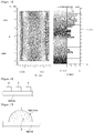
- Figs. 16 and 17 are cross sectional views showing schematically a conventional light source emitting white light.
- the conventional light source shown in Fig. 16 includes a substrate and a blue (B) LED chip, a green (G) LED chip and a red (R) LED chip which are disposed on the substrate.
- the blue (B) LED chip, the green (G) LED chip and the red (R) LED chip emit blue light, green light and red light respectively. The three emitted lights are mixed with each other and become white light.
- the conventional light source shown in Fig. 17 includes a substrate and a blue LED chip and a yellow (Y) fluorescent material which are disposed on the substrate.
- the yellow (Y) fluorescent material uses the blue LED chip as an excitation light source.
- the yellow (Y) fluorescent material is excited by blue light emitted from the blue LED chip and emits yellow light.
- the emitted yellow light and the blue light from the blue LED chip are mixed with each other and become white light.
- the conventional light sources shown in Figs. 16 and 17 emit white light.
- Wavelength-based luminosities of the conventional light sources shown in Figs. 16 and 17 will be described with reference to Figs. 18 and 19 .
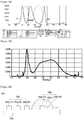
- Fig. 18 is a graph showing a wavelength-based luminosity of the conventional light source shown in Fig. 16 .
- a wavelength-based luminosity of the conventional light source including a blue (B) LED chip, a green (G) LED chip and a red (R) LED chip.
- the blue (B) LED chip has a maximum luminosity at a wavelength of about 450 nm to 460 nm
- the green (G) LED chip has a maximum luminosity at a wavelength of about 510 nm to 530
- the red (R) LED chip has a maximum luminosity at a wavelength of about 625 nm to 635 nm.
- a multichip solution which implements a light source emitting white light by using the R LED chip, the G LED chip and the B LED chip has the advantage of creating various colored lights in accordance with composition ratio of the R LED chip, the G LED chip and the B LED chip.
- light with wavelengths denoted by a dotted-line is not emitted. Therefore, the light source emitting white light by using the R LED chip, the LED G chip and the B LED chip has insufficient spectrum at wavelengths of about 470 nm to 490 nm and 540 nm to 620 nm, and then has poor color rendering property.
- Fig. 19 is a graph showing a wavelength-based luminosity of the conventional light source shown in Fig. 17 .
- the conventional light source including blue (B) LED chip and the yellow (Y) fluorescent material has high luminosity at a wavelength of 450 nm and has low luminosity at a wavelength of about 480 nm to 500 nm.
- the conventional light source has considerable luminosity up to a wavelength of 500 nm to 680 nm. Accordingly, light with a wavelength greater than 500 nm has no problem to reproduce color rendering property.
- a light emitting module or a lighting module which makes use of the conventional light sources shown in Figs. 16 and 17 has, as described above, difficulty in forming a full spectrum having excellent color rendering property.
- a light source according to embodiments, which is able to overcome such problems, will be described below in detail.
- Fig. 20 is a cross sectional view showing schematically a light source 500-1 according to the first embodiment.
- the light source 500-1 according to the first embodiment comprises the substrate 510a, a first light emitter 531a and a second light emitter 533a which are disposed on the substrate 510a.
- the first light emitter 531a comprises a blue (B) LED chip 531a-1, a green (G) LED chip 531a-2, and a red (R) LED chip 531a-3.
- the second light emitter 533a comprises a blue (B) LED chip 533a-1, a yellow (Y) fluorescent material 533a-2 and a resin packer 533a-3.
- the resin packer 533a-3 may be formed to have a hemispherical shape functioning as a lens.
- the resin packer 533a-3 may be formed of epoxy resin, silicone resin, hybrid resin or the like.
- the resin packer 533a-3 may have not only the hemispherical shape but also an elliptical shape and a shape having a predetermined curved portion.
- the LED chip is directly mounted on the substrate in the form of chip on board, so that the first and the second light emitters 531a and 533a may obtain greater orientation angle.
- An electrode pattern or a circuit pattern (not shown) is formed on the substrate 510a.
- the circuit pattern may be connected to an electrode of the LED chip by means of, for example, wire bonding or flip-chip bonding and the like.
- the light source 500-1 comprises a plurality of the light emitters 531a and 533a, and then forms a surface light source or a line light source which has a desired area. Therefore, the light source 500-1 can be used as a lighting device, a backlight unit or the like.
- the first light emitter 531a uses the blue (B) LED chip 531a-1, the green (G) LED chip 531a-2 and the red (R) LED chip 531a-3.
- the first light emitter 531a is not formed by using a fluorescent material in the blue LED chip. This is because when the first light emitter 531a is formed by using the blue (B) LED chip 531a-1, the green (G) LED chip 531a-2 and the red (R) LED chip 531a-3, it is possible to achieve various color changes by controlling the brightness of each LED.
- the resin packer 533a-3 seals the blue (B) LED chip 533a-1.
- the resin packer 533a-3 comprises the yellow (Y) fluorescent material 533a-2.
- the blue light of the blue (B) LED chip 533a-1 is mixed with yellow light emitted from the yellow (Y) fluorescent material 533a-2, and then becomes white light.
- the yellow (Y) fluorescent material 533a-2 may be formed of at least one particle-like material of a YAG fluorescent material, a TAG fluorescent material, an orthosilicate fluorescent material, a silicate fluorescent material, a nitride fluorescent material or an oxynitride fluorescent material.
- the second light emitter 533a is able to form a full spectrum having excellent color rendering property.
- a peak wavelength of the blue (B) LED chip 533a-1 of the second light emitter 533a is changed into 470 nm to 490 nm from existing 450 nm. By doing this, it is possible to cover the spectrum at a wavelength of 470 nm to 490 nm of Fig. 19 .
- Fig. 21 is a cross sectional view showing schematically a light source 500-2 according to the second embodiment.
- a second light emitter 533a' according to the second embodiment comprises a green (G) fluorescent material 533a-2' and a red (R) fluorescent material 533a-2".
- the green (G) fluorescent material 533a-2' and the red (R) fluorescent material 533a-2" are excited by the blue (B) LED chip 533a-1 and emit green light and red light respectively.
- the green light and the red light are mixed with a part of blue light emitted from the blue (B) LED chip 533a-1, and then becomes white light.
- the green (G) fluorescent material 533a-2' may be a silicate fluorescent material (e.g., (Ba,Sr) 2 SiO 4 :Eu) including A 2 SiO 4 :Eu (A is any one selected from among Ba, Sr and Ca).
- SrGa 2 S 4 :Eu or ⁇ -SiAlON(Beta-SiAlON) may be used as the green (G) fluorescent material 533a-2'.
- the red (R) fluorescent material 533a-2" may be a nitride fluorescent material like Ca 2 Si 5 N 8 :Eu, etc., or a sulfide fluorescent material like (Ca,Sr)S:Eu, etc., in order to obtain high color reproductivity.
- the light sources 500-1 and 500-2 according to the first and the second embodiments are able to form a full spectrum without adding a cyan LED chip and to prevent color reproduction range from being reduced when a peak wavelength of the blue (B) LED chip 531a-1 of the first light emitter 531a is changed into 470 nm to 490 nm.
- Fig. 22 is a cross sectional view showing schematically a light source 500-3 according to a third embodiment.
- the light source 500-3 comprises the substrate 510a, a first light emitter 531a and a second light emitter 533a" which are disposed on the substrate 510a.
- the first light emitter 531a is the same as the first light emitter 531a shown in Fig. 20 .
- a yellow (Y) fluorescent material film 533a-4 is coated on the blue (B) LED chip 533a-1, and then the hemispherical transparent resin packer 533a-3 is disposed on the blue (B) LED chip 533a-1.
- a yellow (Y) fluorescent material film 533a-5 including the yellow (Y) fluorescent material is coated on the transparent resin packer 533a-3.
- a peak wavelength of the blue (B) LED chip 533a-1 of the second light emitter 533a" is from 470 nm to 490 nm.
- the peak wavelength of the blue (B) LED chip 533a-1 is from 470 nm to 490 nm, it is possible to cover the wavelength of 470 nm to 490 nm of Fig. 19 .
- Fig. 23 is a cross sectional view showing schematically a light source 500-4 according to a fourth embodiment.
- a second light emitter 533a''' according to the fourth embodiment comprises a red (R) fluorescent material film 533a-4' and a green (G) fluorescent material film 533a-5'.
- the red (R) fluorescent material film 533a-4' may be coated on the blue (B) LED chip 533a-1.
- the green (G) fluorescent material film 533a-5' may be coated on the resin packer 533a-3.
- the green (G) fluorescent material film may be coated on the blue (B) LED chip 533a-1.
- the red (R) fluorescent material film may be coated on the resin packer 533a-3.
- the light source 500-4 comprises the red fluorescent material film 533a-4', the transparent resin packer 533a-3 and the green fluorescent material film 533a-5', thereby more improving the color uniformity of the emitted white light. If the green and the red fluorescent materials are simply dispersed within the resin packer 533a-3, it is expected that the fluorescent materials are not uniformly dispersed and layers of the fluorescent materials are formed and separated due to the difference in specific gravities of the fluorescent materials during a resin curing process. As a result, there is a possibility that the color uniformity is reduced. However, in the light source according to the fourth embodiment shown in Fig. 23 , blue light emitted at various angles from the blue (B) LED chip 533a-1 is relatively uniformly absorbed or transmitted through the fluorescent material film 533a-4' and 533a-5', so that it is possible to obtain overall more uniform white light.
- the second light converted by the fluorescent material film 533a-4' transmits through the transparent resin packer 533a-3, and the second light converted by the fluorescent material film 533a-5' is emitted to the outside of the second light emitter 533a"'. Accordingly, it is possible to reduce optical loss caused by the particles of fluorescent material.
- the peak wavelengths of the blue (B) LED chips 533a-1 of the second light emitters 533a" and 533a''' are changed into 470 nm to 490 nm, so that it is possible to form a full spectrum having high color reproductivity.
- Fig. 24 is a cross sectional view showing schematically a light source 500-5 according to a fifth embodiment.
- the light source 500-5 according to the fifth embodiment comprises the substrate 510a, the first light emitter 531a' and a second light emitter 533a'''' which are disposed on the substrate 510a.
- the first light emitter 531a' may comprise the blue (B) LED chip 531a-1, the green (G) LED chip 531a-2, the red (R) LED chip 531a-3 and a body 531a-5.
- the body 531a-5 has a predetermined cavity.
- the blue (B) LED chip 531a-1, the green (G) LED chip 531a-2 and the red (R) LED chip 531a-3 are disposed within the cavity.
- the second light emitter 533a'''' may comprise the blue (B) LED chip 533a-1, the yellow (Y) fluorescent material 533a-2, a resin packer 533a-3' and a body 533a-7.
- the body 533a-7 has a predetermined cavity.
- the blue (B) LED chip 533a-1, the yellow (Y) fluorescent material 533a-2, the resin packer 533a-3' are disposed within the cavity.
- the yellow (Y) fluorescent material 533a-2 is mixed within the resin packer 533a-3'.
- the blue (B) LED chip 533a-1 is buried within the resin packer 533a-3'.
- Fig. 25 is a cross sectional view showing schematically a light source 500-6 according to a sixth embodiment.
- a second light emitter 533a''''' according to the sixth embodiment comprises the green (G) fluorescent material 533a-2' and the red (R) fluorescent material 533a-2".
- the light sources 500-5 and 500-6 according to the fifth and the sixth embodiments are able to form a full spectrum without adding a cyan LED chip and to prevent color reproduction range from being reduced when a peak wavelength of the blue (B) LED chip 531a-1 of the first light emitter 531a' is changed into 470 nm to 490 nm.
- Fig. 26 is a cross sectional view showing schematically a light source 500-7 according to a seventh embodiment.
- the light source 500-7 according to the seventh embodiment comprises the substrate 510a, a first light emitter 531a' and a second light emitter 533a''''' which are disposed on the substrate 510a.
- the first light emitter 531a' is the same as the first light emitter 531a' shown in Fig. 25 .
- the yellow (Y) fluorescent material film 533a-4 is coated on the blue (B) LED chip 533a-1, and then the hemispherical transparent resin packer 533a-3' is disposed on the blue (B) LED chip 533a-1.
- the yellow (Y) fluorescent material film 533a-5 including the yellow (Y) fluorescent material is coated on the transparent resin packer 533a-3'.
- a peak wavelength of the blue (B) LED chip 533a-1 of the second light emitter 533a''''' is from 470 nm to 490 nm.
- the peak wavelength of the blue (B) LED chip 533a-1 is from 470 nm to 490 nm, it is possible to cover the wavelength of 470 nm to 490 nm of Fig. 19 .
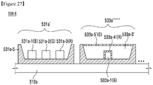
- Fig. 27 is a cross sectional view showing schematically a light source 500-8 according to an eighth embodiment.
- a second light emitter 533a''''''' according to the eighth embodiment comprises the red (R) fluorescent material film 533a-4' and the green (G) fluorescent material film 533a-5'.
- the red (R) fluorescent material film 533a-4' may be coated on the blue (B) LED chip 533a-1.
- the green (G) fluorescent material film 533a-5' may be coated on the resin packer 533a-3.
- the green (G) fluorescent material film may be coated on the blue (B) LED chip 533a-1.
- the red (R) fluorescent material film may be coated on the resin packer 533a-3.
- the light source 500-8 comprises the red fluorescent material film 533a-4', the transparent resin packer 533a-3' and the green fluorescent material film 533a-5', thereby more improving the color uniformity of the emitted white light.
- blue light emitted at various angles from the blue (B) LED chip 533a-1 is relatively uniformly absorbed or transmitted through the fluorescent material film 533a-4' and 533a-5', so that it is possible to obtain overall more uniform white light.
- the fluorescent material film 533a-4' and 533a-5' which are separated from each other by the transparent resin packer 533a-3' are used, it is possible to reduce optical loss caused by the fluorescent material. More specifically, in the light source according to the eighth embodiment shown in Fig. 27 , the second light converted by the fluorescent material film 533a-4' transmits through the transparent resin packer 533a-3', and the second light converted by the fluorescent material film 533a-5' is emitted to the outside of the second light emitter 533a''''''. Accordingly, it is possible to reduce optical loss caused by the particles of fluorescent material.
Description
- Embodiments relate to a lighting module.
- In general, an electric bulb or a fluorescent lamp is commonly used as an indoor or outdoor lighting lamp. However, the electric bulb or the fluorescent lamp has a short life span, so that it should be frequently changed. Moreover, a conventional fluorescent lamp is degraded due to elapse of time for its use. As a result, it is often that its illuminance is gradually decreased.
- In order to overcome such problems, a lighting apparatus is now being developed by using a light emitting device, see
US2006203512 A1 (hereinafter, referred to as LED). The LED is easy to control and has a rapid response speed, high electro-optic conversion efficiency, a long life span, low power consumption and high luminance. The LED is also used to create emotional lighting. - The objective of the present invention is to provide a lighting module which does not use a light guide plate.
- The objective of the present invention is to provide a lighting module capable of controlling light distribution.
- The objective of the present invention is to provide a lighting module of which the lamp apparatus efficiency is higher than 80 % and the height (thickness) is less than 20 mm.
- The objective of the present invention is to provide a lighting module including a light source which has a high color rendering property.
- The objective of the present invention is to provide a lighting module including a light source which has high color reproductivity and excellent color uniformity.
- One embodiment is a lighting module. The lighting module comprises: an optical plate; a base frame including a central frame disposed on the optical plate, a first frame coupled to the central frame, and a second frame coupled to the first frame; a side frame coupled between the optical plate and the second frame of the base frame; and a light source including a substrate disposed on the side frame and a light emitter disposed on the substrate. The second frame is disposed on the light source. The second frame has an inner surface reflecting light from the light source to at least one of the first frame and the central frame.
- The cross sectional shape of the inner surface of the second frame is at least one of a parabolic shape, a hyperbolic shape and an elliptical shape.
- The thickness of the central frame is larger than that of the first frame.
- The thickness of the first frame becomes larger toward the central frame from the second frame.
- The thickness of the central frame becomes larger toward the center of the central frame from one side of the central frame.
- The inner surface of the first frame becomes closer to the optical plate toward the central frame from the second frame.
- The inner surface of the central frame becomes closer to the optical plate toward the center of the central frame from one side of the central frame.
- The side frame comprises a coupler which is coupled to one side of the optical plate.
- The light emitter of the light source comprises: a first light emitter disposed on the substrate; and a second light emitter disposed on the substrate and around the first light emitter. The first light emitter comprises a red LED chip, a green LED chip and a first blue LED chip. The second light emitter comprises a second blue LED chip having a wavelength of from 470 nm to 490 nm; and a yellow fluorescent material disposed around the second blue LED chip.
- The second light emitter comprises: a first fluorescent material film which is disposed on the second blue LED chip and comprises the yellow fluorescent material; a resin packer which is disposed on the first fluorescent material film; and a second fluorescent material film which is disposed on the resin packer and comprises the yellow fluorescent material.
- The first light emitter further comprises a first body in which the red LED chip, the green LED chip and the first blue LED chip are disposed. The second light emitter further comprises a second body in which the second blue LED chip and the yellow fluorescent material are disposed.
- The light emitter of the light source comprises: a first light emitter disposed on the substrate; and a second light emitter disposed on the substrate and around the first light emitter. The first light emitter comprises a red LED chip, a green LED chip and a first blue LED chip. The second light emitter comprises a second blue LED chip having a wavelength of from 470 nm to 490 nm; and at least one of a red fluorescent material and a green fluorescent material which are disposed around the second blue LED chip.
- The second light emitter comprises: a first fluorescent material film which is disposed on the second blue LED chip and comprises any one of the red fluorescent material and the green fluorescent material; a resin packer which is disposed on the first fluorescent material film; and a second fluorescent material film which is disposed on the resin packer and comprises any one of the red fluorescent material and the green fluorescent material.
- The first light emitter further comprises a first body in which the red LED chip, the green LED chip and the first blue LED chip are disposed. The second light emitter further comprises a second body in which the second blue LED chip and any one of the red fluorescent material and the green fluorescent material are disposed.
- Another embodiment is a lighting module. The lighting module comprises: an optical plate; a base frame including a central frame disposed on the optical plate, a first frame coupled to the central frame, and a second frame coupled to the first frame; a side frame coupled between the optical plate and the second frame of the base frame; and a light source including a substrate disposed on the side frame in such a manner as to be perpendicular to the optical plate, and a light emitter disposed on the substrate.
- The side frame comprises: a first side frame on which the substrate of the light source is disposed and which is coupled to the second frame of the base frame; and a second side frame which is coupled to the first side frame and is coupled to optical plate.
- *25The second frame of the base frame has a recess receiving one side of the substrate of the light source. The second side frame of the side frame has a recess receiving the other side of the substrate of the light source.
- The second side frame of the side frame comprises a coupler which is coupled to a portion of the optical plate.
- The thickness of the first frame of the base frame is uniform. The thickness of the central frame is larger than that of the first frame. The inner surface of the first frame comprises a predetermined roughness.
- The cross sectional shape of the central frame of the base frame is a hemisphere or a semi-ellipse.
- A lighting module according to the embodiment does not use a light guide plate, thereby causing the lighting module to be lighter and to have a low unit cost.
- A lighting module according to the embodiment is capable of controlling light distribution.
- A lighting module according to the embodiment has a lamp apparatus efficiency higher than 80 % and height (thickness) less than 20 mm
- A lighting module according to the embodiment is capable of providing white light having a high color rendering property by creating a full spectrum based on wavelengths.
- A lighting module according to the embodiment is capable of providing high color reproductivity and excellent color uniformity.
-
-
Fig. 1 is a top perspective view of a lighting module according to a first embodiment; -
Fig. 2 is a bottom perspective view of the lighting module shown inFig. 1 ; -
Fig. 3 is an exploded perspective view of the lighting module shown inFig. 2 ; -
Fig. 4 is a cross sectional view of the lighting module shown inFig. 1 ; -
Fig. 5 is a view for describing a traveling path of light when an inner surface of a second frame shown inFig. 4 has a parabolic shape; -
Fig. 6 is a view for describing a traveling path of light when the inner surface of a second frame shown inFig. 4 has a hyperbolic shape; -
Fig. 7 is a view for describing a traveling path of light when the inner surface of a second frame shown inFig. 4 has an elliptical shape; -
Fig. 8 is a graph showing an optical characteristic of the lighting module shown inFigs. 1 to 4 ; -
Fig. 9 is a view showing a luminous flux distribution of the lighting module shown inFigs. 1 to 4 ; -
Fig. 10 is a top perspective view of a lighting module according to a second embodiment; -
Fig. 11 is a bottom perspective view of the lighting module shown inFig. 10 ; -
Fig. 12 is an exploded perspective view of the lighting module shown inFig. 11 ; -
Fig. 13 is a cross sectional view of the lighting module shown inFig. 10 ; -
Fig. 14 is a graph showing an optical characteristic of the lighting module shown inFigs. 10 to 13 ; -
Fig. 15 is a view showing a luminous flux distribution of the lighting module shown inFigs. 10 to 13 ; -
Figs. 16 and 17 are cross sectional views showing schematically a conventional light source emitting white light; -
Fig. 18 is a graph showing a wavelength-based luminosity of the conventional light source shown inFig. 16 ; -
Fig. 19 is a graph showing a wavelength-based luminosity of the conventional light source shown inFig. 17 ; -
Fig. 20 is a cross sectional view showing schematically a light source 500-1 according to the first embodiment; -
Fig. 21 is a cross sectional view showing schematically a light source 500-2 according to the second embodiment; -
Fig. 22 is a cross sectional view showing schematically a light source 500-3 according to a third embodiment; -
Fig. 23 is a cross sectional view showing schematically a light source 500-4 according to a fourth embodiment; -
Fig. 24 is a cross sectional view showing schematically a light source 500-5 according to a fifth embodiment; -
Fig. 25 is a cross sectional view showing schematically a light source 500-6 according to a sixth embodiment; -
Fig. 26 is a cross sectional view showing schematically a light source 500-7 according to a seventh embodiment; and -
Fig. 27 is a cross sectional view showing schematically a light source 500-8 according to an eighth embodiment. - A thickness or size of each layer is magnified, omitted or schematically shown for the purpose of convenience and clearness of description. The size of each component does not necessarily mean its actual size.
- In description of embodiments of the present invention, when it is mentioned that an element is formed "on" or "under" another element, it means that the mention includes a case where two elements are formed directly contacting with each other or are formed such that at least one separate element is interposed between the two elements. The "on" and "under" will be described to include the upward and downward directions based on one element.
- Hereafter, a lighting module according to an embodiment will be described with reference to the accompanying drawings.
-
Fig. 1 is a top perspective view of a lighting module according to a first embodiment.Fig. 2 is a bottom perspective view of the lighting module shown inFig. 1 .Fig. 3 is an exploded perspective view of the lighting module shown inFig. 2 .Fig. 4 is a cross sectional view of the lighting module shown inFig. 1 . - Referring to
Figs. 1 to 4 , the lighting module according to the first embodiment may comprise abase frame 100,side frames light sources optical plate 700. - The
base frame 100 may have a plate shape having an outer surface and an inner surface. The outer surface of thebase frame 100 forms the appearance of the lighting module according to the embodiment. The inner surface of thebase frame 100 is disposed within the lighting module according to the embodiment and reflects light from thelight sources optical plate 700. - The
base frame 100 may comprise a plurality of frames. Specifically, thebase frame 100 may comprise acentral frame 110,first frames second frames - The
central frame 110 is disposed at the center of thebase frame 100. Thecentral frame 110 reflects the light from thelight sources optical plate 700. For this purpose, an inner surface of thecentral frame 110 may project outwardly or may be convex. The inner surface of thecentral frame 110 becomes closer to theoptical plate 700 toward the center of thecentral frame 110 from both sides of thecentral frame 110. Also, thecentral frame 110 becomes thicker toward the center of thecentral frame 110 from both sides of thecentral frame 110. - The
first frames first frame 130a and a second sidefirst frame 130b. One side of the first sidefirst frame 130a is coupled to one side of both sides of thecentral frame 110. One side of the second sidefirst frame 130b is coupled to the other side of both sides of thecentral frame 110. Here, thefirst frames central frame 110 may be integrally formed with each other. - The first side
first frame 130a may become thicker toward thecentral frame 110 from thesecond frame 150a. Contrarily, the first sidefirst frame 130a may become thinner toward thesecond frame 150a from thecentral frame 110. Also, an inner surface of the first sidefirst frame 130a becomes closer to theoptical plate 700 toward thecentral frame 110 from thesecond frame 150a. Contrarily, the inner surface of the first sidefirst frame 130a becomes farther from theoptical plate 700 toward thesecond frame 150a from thecentral frame 110. - The
central frame 110 is thicker than thefirst frame 130a. Also, a distance from the inner surface of thecentral frame 110 to theoptical plate 700 is less than a distance from the inner surface of thefirst frame 130a to theoptical plate 700. - The inner surface of the first side
first frame 130a may reflect light, which is directly or indirectly incident from thefirst light source 500a, to thecentral frame 110 and theoptical plate 700. An inner surface of the second sidefirst frame 130b may reflect light, which is directly or indirectly incident from the secondlight source 500b, to thecentral frame 110 and theoptical plate 700. - The
second frames second frame 150a and a second sidesecond frame 150b. The first sidesecond frame 150a is coupled to the other side of the first sidefirst frame 130a. The second sidesecond frame 150b is coupled to the other side of the second sidefirst frame 130b. Here, thesecond frames first frames first frames central frame 110. - An inner surface of the first side
second frame 150a reflects the light from thefirst light source 500a to the first sidefirst frame 130a, thecentral frame 110 and theoptical plate 700. An inner surface of the second sidesecond frame 150b reflects the light from the secondlight source 500b to the second sidefirst frame 130b, thecentral frame 110 and theoptical plate 700. - The inner surfaces of the
second frames second frames Figs. 5 to 7 . -
Fig. 5 is a view for describing a traveling path of light when an inner surface of a second frame shown inFig. 4 has a parabolic shape. - Referring to
Figs. 4 and 5 , the inner surfaces of thesecond frames devices second frames light emitting devices optical plate 700. Therefore, the light reflected by the inner surfaces of thesecond frames first frames central frame 110. Thesecond frames central frame 110. -
Fig. 6 is a view for describing a traveling path of light when the inner surface of a second frame shown inFig. 4 has a hyperbolic shape. - Referring to
Figs. 4 and 6 , the inner surfaces of thesecond frames light emitting devices second frames light emitting devices second frames first frames first frames second frames -
Fig. 7 is a view for describing a traveling path of light when the inner surface of a second frame shown inFig. 4 has an elliptical shape. - Referring to
Figs. 4 and7 , the inner surfaces of thesecond frames light emitting devices second frames light emitting devices second frames first frames central frame 110. - Referring back to
Figs. 1 to 4 , the side frames 300a and 300b are disposed on both side of thecentral base 110 respectively. The side frames 300a and 300b may comprise afirst side frame 300a and asecond side frame 300b. Thefirst side frame 300a may be coupled to the first sidesecond frame 150a of thebase frame 100. Thesecond side frame 300b may be coupled to the second sidesecond frame 150b of thebase frame 100. - The
first side frame 300a and thesecond side frame 300b support both sides of thebase frame 100 and both sides of theoptical plate 700, so that thebase frame 100 and theoptical plate 700 can be spaced apart from each other. - The
first side frame 300a and thesecond side frame 300b receive thefirst light source 500a and the secondlight source 500b. Specifically, thefirst side frame 300a receives thefirst light source 500a. Thesecond side frame 300b receives the secondlight source 500b. - The
first side frame 300a is coupled to the first sidesecond frame 150a of thebase frame 100 and is coupled to one side of theoptical plate 700. Thesecond side frame 300b is coupled to the second sidesecond frame 150b of thebase frame 100 and is coupled to the other side of theoptical plate 700. Thefirst side frame 300a may comprise afirst_A side frame 310a and asecond_A side frame 330a. Thefirst_A side frame 310a is coupled to thebase frame 100. Thesecond_A side frame 330a is coupled to one side of theoptical plate 700. - *88The
first_A side frame 310a and thesecond_A side frame 330a may have a plate shape respectively and may form a predetermined angle. Thefirst_A side frame 310a and thesecond_A side frame 330a may be formed in correspondence with the shapes of thesecond frames first_A side frame 310a and thesecond_A side frame 330a may be substantially perpendicular to each other. Here, thefirst_A side frame 310a and thesecond_A side frame 330a may be integrally formed with each other and they can be distinguished as thefirst_A side frame 310a and thesecond_A side frame 330a by bending thefirst side frame 300a. - An inner surface of the
first_A side frame 310a may come in surface contact with and may be coupled to an outer surface of the first sidesecond frame 150a of thebase frame 100. Through the surface contact, heat radiated from thefirst light source 500a can be transferred to thebase frame 100. - The
second_A side frame 330a is coupled to one side of theoptical plate 700. Specifically, thesecond_A side frame 330a may have a structure capable of receiving the one side of theoptical plate 700. For example, thesecond_A side frame 330a may have acoupler 335a allowing thesecond_A side frame 330a to be coupled to the one side of theoptical plate 700. Thanks to thecoupler 335a, theoptical plate 700 can be coupled to thesecond_A side frame 330a in a sliding manner. - The
first light source 500a is disposed in thesecond_A side frame 330a. Thefirst light source 500a disposed in thesecond_A side frame 330a emits light toward thebase frame 100. Thesecond_A side frame 330a may be disposed in parallel with theoptical plate 700. When thesecond_A side frame 330a is disposed in parallel with theoptical plate 700, the position of thefirst light source 500a may be specified. - Since the structure of the
second side frame 300b is the same as that of the above-describedfirst side frame 300a, a detailed description thereof will be replaced by the foregoing description. - The
first side frame 300a and thesecond side frame 300b may be formed of a material capable of easily radiating the heat from thefirst light source 500a and the secondlight source 500b. For example, thefirst side frame 300a and thesecond side frame 300b may be formed of Al, an alloy including Al, and the like. Here, thebase frame 100 may be also formed of the same heat radiating material as those of thefirst side frame 300a and thesecond side frame 300b. However, there is no limit to this. Thebase frame 100 may be formed of a material different from those of thefirst side frame 300a and thesecond side frame 300b. - The
light sources first light source 500a disposed in thefirst side frame 300a, and the secondlight source 500b disposed in thesecond side frame 300b. Here, since the secondlight source 500b is the same as thefirst light source 500a, a description of the secondlight source 500b will be replaced by the following description of thefirst light source 500a. - The
first light source 500a may comprise asubstrate 510a and thelight emitting device 530a. - A plurality of the
light emitting devices 530a may be disposed on one side of thesubstrate 510a in a row or may be disposed adjacent to each other. The other side of thesubstrate 510a is disposed in thesecond_A side frame 330a of thefirst side frame 300a. - The
substrate 510a and theoptical plate 700 may be disposed on the same plane with each other. Otherwise, thesubstrate 510a may be disposed in parallel with theoptical plate 700. Also, thesubstrate 510a may be disposed in parallel with the outer surface of thebase frame 100. - The
substrate 510a may comprise a printed circuit board (PCB), a metal core PCB (MCPCB), a flexible PCB (FPCB), a ceramic substrate or the like. - The
light emitting device 530a may be a light emitting diode (LED). A position on which thelight emitting device 530a is disposed on thesubstrate 510a may be changed according to the cross sectional shapes of thesecond frames base frame 100. That is, when the cross sectional shapes of thesecond frames light emitting device 530a may be disposed at a position corresponding to the foci of the parabola, hyperbola and ellipse. However, there is no limit to this. Thelight emitting device 530a may not be disposed at the position corresponding to the foci of the parabola, hyperbola and ellipse. - The plurality of the
light emitting devices 530a may emit the same colored light or differently colored lights. - The
light emitting device 530a may be a blue light emitting device or a white light emitting device having a high color rendering index (CRI). Synthetic resin including a fluorescent material is molded on a blue light emitting chip, so that the white light emitting device emits white light. Here, the fluorescent material may comprise at least any one selected from a group consisting of a garnet material (YAG, TAG), a silicate material, a nitride material and an oxynitride material. Though natural light (white light) can be created by allowing the synthetic resin to comprise only yellow fluorescent material, the synthetic resin may further comprise a green fluorescent material or a red fluorescent material in order to improve a color rendering index and to reduce a color temperature. When the synthetic resin is mixed with many kinds of fluorescent materials, an addition ratio of the color of the fluorescent material may be formed such that the green fluorescent material is more used than the red fluorescent material, and the yellow fluorescent material is more used than the green fluorescent material. The garnet material, the silicate material and the oxynitride material may be used as the yellow fluorescent material. The silicate material and the oxynitride material may be used as the green fluorescent material. The nitride material may be used as the red fluorescent material. The synthetic resin may be mixed with various kinds of the fluorescent materials or may be configured by a layer including the red fluorescent material, a layer including the green fluorescent material and a layer including the yellow fluorescent material, which are formed separately from each other. - The
first light source 500a may further comprise a heat radiation sheet (not shown). The heat radiation sheet (not shown) may be disposed between thesubstrate 510a and thefirst side frame 300a. The heat radiation sheet (not shown) may rapidly transfer the heat from thesubstrate 510a to thefirst side frame 300a. - The
light emitting devices 530a of thefirst light source 500a may have a color temperature different from that of thelight emitting devices 530b of the secondlight source 500b. For example, a plurality of thelight emitting devices 530a comprised in thefirst light source 500a may be a warm white LED, and a plurality of thelight emitting devices 530b comprised in the secondlight source 500b may be a cool white LED. The warm white LED and the cool white LED emit white light. Since the warm white LED and the cool white LED are able to emit mixed white light by emitting a correlated color temperature respectively, a color rendering index (CRI) representing how close light is to natural sunlight becomes larger. Accordingly, it is possible to prevent an actual color of an object from being distorted and to reduce fatigue of the eyes of a user. - The
optical plate 700 transmits the light which has been emitted from thelight sources base frame 100. - The
optical plate 700 may have a plate shape having an outer surface and an inner surface. The one side of theoptical plate 700 may be coupled to thefirst side frame 300a. The other side of theoptical plate 700 may be coupled to thesecond side frame 300b. - The
optical plate 700 may allow the light incident from thebase frame 100 to pass therethrough as it is. Otherwise, theoptical plate 700 may diffuse the light incident from thebase frame 100. For this purpose, theoptical plate 700 may comprise a diffusion material. - The
optical plate 700 may have a predetermined pattern for the purpose of more improving light diffusion rate. The pattern may have a concave lens shape or a convex lens shape. - The
optical plate 700 may be transparent, opaque or translucent. - The
optical plate 700 may emit light which is excited by the incident light and has a wavelength different from that of the incident light. For this, theoptical plate 700 may have a fluorescent material. The fluorescent material may comprise at least any one of a yellow fluorescent material, a green fluorescent material and a red fluorescent material. -
Fig. 8 is a graph showing an optical characteristic of the lighting module according to the first embodiment shown inFigs. 1 to 4 .Fig. 9 is a view showing a luminous flux distribution of the lighting module according to the first embodiment shown inFigs. 1 to 4 . - Referring to
Figs. 8 and9 , it can be seen that uniformity, efficiency and a beam angle of the light emitted from the lighting module according to the first embodiment are about 83.3 %, about 87.2 % and about 110° respectively. - Meanwhile, through the described configuration, a size of the lighting module according to the first embodiment shown in
Figs. 1 to 4 may be reduced. Specifically, the size and height of the lighting module according to the first embodiment may be within 300×600 (mm) and 20 mm respectively. -
Fig. 10 is a top perspective view of a lighting module according to a second embodiment.Fig. 11 is a bottom perspective view of the lighting module shown inFig. 10 .Fig. 12 is an exploded perspective view of the lighting module shown inFig. 11 .Fig. 13 is a cross sectional view of the lighting module shown inFig. 10 . - Referring to
Figs. 10 to 13 , the lighting module according to the second embodiment comprises a base frame 100',side frame 300a' and 300b',light sources 500a' and 500b', and anoptical plate 700. Here, since theoptical plate 700 is the same as theoptical plate 700 shown inFigs. 1 to 4 , a detailed description thereof will be omitted. - Hereafter, regarding the base frame 100', the side frames 300a' and 300b', and the
light sources 500a' and 500b', descriptions of the same parts as those of thebase frame 100, the side frames 300a and 300b, thelight sources Figs. 1 to 4 will be omitted, and different parts will be described below in detail. - The base frame 100' may comprise a central frame 110',
first frames 130a' and 130b', andsecond frames 150a' and 150b'. - A cross section of the central frame 110' may have a hemispherical shape. In this specification, the hemispherical shape includes not only a geometrically perfect hemispherical shape but also a semi-elliptical shape.
- The
first frames 130a' and 130b' comprise a first sidefirst frame 130a' and a second sidefirst frame 130b'. - Unlike the
first frames Figs. 1 to 4 , thefirst frames 130a' and 130b' may have a uniform thickness. - Inner surfaces of the
first frames 130a' and 130b' may have predetermined roughnesses 135a' and 135b'. The cross sectional shapes of the roughnesses 135a' and 135b' may be various, for example, a hemisphere, a semi-ellipse, a polygon or the like. Due to the roughnesses 135a' and 135b', light from thelight sources 500a' and 500b' can be reflected toward theoptical plate 700. - The minimum thickness of the central frame 110' is larger than the thickness of the
first frame 130a'. Here, the minimum thickness of the central frame 110' may be the same as or larger than the thickness of thefirst frame 130a'. A distance from an inner surface of the central frame 110' to theoptical plate 700 is less than a distance from the inner surface of thefirst frame 130a' to theoptical plate 700. Here, a distance from the thickest portion of the central frame 110' to theoptical plate 700 may be less than the distance from thefirst frame 130a' to theoptical plate 700. - The
second frames 150a' and 150b' comprise a first sidesecond frame 150a' and a second sidesecond frame 150b'. The first sidesecond frame 150a' is coupled to the other side of the first sidefirst frame 130a'. The second sidesecond frame 150b' is coupled to the other side of the second sidefirst frame 130b'. Here, thesecond frames 150a' and 150b' may be integrally formed with thefirst frames 130a' and 130b' or may be integrally formed with thefirst frames 130a' and 130b' and the central frame 110'. - An inner surface of the first side
second frame 150a' may reflect the light from thefirst light source 500a' to the first sidefirst frame 130a', the central frame 110' and theoptical plate 700. An inner surface of the second sidesecond frame 150b' may reflect the light from the secondlight source 500b' to the second sidefirst frame 130b', the central frame 110' and theoptical plate 700. For this, thesecond frames 150a' and 150b' may have predetermined curved inner surfaces. The curved surface may have a curvature corresponding to an inner surface of asecond_A side frame 330a'. - The
second frames 150a' and 150b' may have arecess 155a'. One sides of thelight sources 500a' and 500b' may be disposed in therecess 155a'. Thelight sources 500a' and 500b' can be fixed by therecess 155a'. - Specifically, the
recess 155a' and arecess 339a' of afirst side frame 300a' receive both sides of substrates 510a' and 510b' of thelight sources 500a' and 500b'. Here, thesubstrates 510a' and 510b' may be coupled in a sliding manner via therecesses 155a' of thesecond frames 150a' and 150b' and via the recess 339a'of thefirst side frame 300a'. Here, the coupling method of the substrates 510a' and 510b' is not limited to the sliding manner. - The side frames 300a' and 300b' may comprise the
first side frame 300a' and asecond side frame 300b'. - The
first side frame 300a' may comprise afirst_A side frame 310a' and asecond_A side frame 330a'. Thefirst_A side frame 310a' is coupled to the base frame 100'. Thesecond_A side frame 330a' is coupled to one side of theoptical plate 700. - The
first_A side frame 310a' may have a plate shape. Thefirst_A side frame 310a' and thesecond_A side frame 330a' may be substantially perpendicular to each other. Here, an angle between thefirst_A side frame 310a' and thesecond_A side frame 330a' may be changed according to the shapes of thesecond frames 150a' and 150b'. Thefirst_A side frame 310a' and thesecond_A side frame 330a' may be integrally formed with each other and they can be distinguished as thefirst_A side frame 310a' and thesecond_A side frame 330a' by bending thefirst side frame 300a'. - The
first light source 500a' may be disposed on an inner surface of thefirst_A side frame 310a'. Specifically, thesubstrate 510a' of thelight source 500a' is disposed on the inner surface of thefirst_A side frame 310a'. Therefore, the light of thelight source 500a' is emitted upward from the inner surface of thefirst_A side frame 310a'. - The inner surface of the
first_A side frame 310a' may come in surface contact with and may be coupled to an outer surface of the first sidesecond frame 150a' of the base frame 100'. Through this connection, heat from thefirst_A side frame 310a' can be transferred to the base frame 100'. - The
second_A side frame 330a' is coupled to one side of theoptical plate 700. Specifically, thesecond_A side frame 330a' may have a structure capable of receiving the one side of theoptical plate 700. For example, thesecond_A side frame 330a' may have acoupler 335a' allowing thesecond_A side frame 330a to be coupled to the one side of theoptical plate 700. Thanks to thecoupler 335a', theoptical plate 700 can be coupled to thesecond_A side frame 330a' in a sliding manner. Here, the coupling method of theoptical plate 700 is not limited to the sliding manner. - A portion of the inner surface of the
second_A side frame 330a' may be curved. The curved surface of thesecond_A side frame 330a' may have a shape corresponding to the curved surface of thesecond frame 150a of thebase frame 100. - The
second_A side frame 330a' may have therecess 339a' for fixing thefirst light source 500a'. Therecess 339a' receives one side of thesubstrate 510a' of thefirst light source 500a'. Here, thesubstrate 510a' may be coupled to therecess 339a' of thefirst side frame 300a' in a sliding manner. Here, the coupling method of thesubstrates 510a' is not limited to the sliding manner. - Since the structure of the
second side frame 300b' is the same as that of the describedfirst side frame 300a', a detailed description thereof will be replaced by the foregoing description. - The
light sources 500a' and 500b' may comprise thefirst light source 500a' disposed in thefirst side frame 300a' and the secondlight source 500b' disposed in thesecond side frame 300b'. - The
first light source 500a' and the secondlight source 500b' may be disposed corresponding to each other or disposed opposite to each other. Specifically, alight emitting device 530a' of thefirst light source 500a' and alight emitting device 530b' of the secondlight source 500b' may be disposed corresponding to each other or disposed opposite to each other. - The central frame 110' of the base frame 100' may be disposed between the
first light source 500a' and the secondlight source 500b'. Therefore, when the central frame 110' has the maximum thickness, the light emitted from thefirst light source 500a' has no effect on the secondlight source 500b', and the light emitted from the secondlight source 500b' has no effect on thefirst light source 500a'. - Since the second
light source 500b' is the same as thefirst light source 500a', a description of the secondlight source 500b' will be replaced by the following description of thefirst light source 500a'. - The
first light source 500a' may comprise thesubstrate 510a' and thelight emitting device 530a'. - A plurality of the
light emitting devices 530a' may be disposed on one side of thesubstrate 510a' in a row. The other side of thesubstrate 510a' is disposed on the inner surface of thefirst_A side frame 310a' of thefirst side frame 300a'. - One side of the
substrate 510a' may be received in therecess 339a' of thesecond_A side frame 330a' of thefirst side frame 300a'. The other side of thesubstrate 510a' may be received in therecess 155a' of thesecond frame 150a' of the base frame 100'. Accordingly, thesubstrate 510a' may be coupled to thefirst side frame 300a' in a sliding manner. Here, the coupling method of thesubstrate 510a' is not limited to the sliding manner. -
Fig. 14 is a graph showing an optical characteristic of the lighting module according to the second embodiment shown inFigs. 10 to 13 .Fig. 15 is a view showing a luminous flux distribution of the lighting module according to the second embodiment shown inFigs. 10 to 13 . - Referring to
Figs. 14 and15 , it can be seen that uniformity, efficiency and a beam angle of the light emitted from the lighting module according to the second embodiment are about 87.3 %, about 83.2 % and about 115° respectively. - Meanwhile, through the described configuration, a size of the lighting module according to the second embodiment shown in
Figs. 10 to 13 may be reduced. Specifically, the size and height of the lighting module according to the second embodiment may be within 300×600 (mm) and 20 mm respectively. -
Figs. 20 to 27 below are views for specifically describing thelight sources Figs. 3 and12 . - Prior to the detailed descriptions of the
light sources Figs. 3 and12 , one example of a conventional light source will be described with reference toFigs. 16 to 19 . -
Figs. 16 and 17 are cross sectional views showing schematically a conventional light source emitting white light. - The conventional light source shown in
Fig. 16 includes a substrate and a blue (B) LED chip, a green (G) LED chip and a red (R) LED chip which are disposed on the substrate. The blue (B) LED chip, the green (G) LED chip and the red (R) LED chip emit blue light, green light and red light respectively. The three emitted lights are mixed with each other and become white light. - The conventional light source shown in
Fig. 17 includes a substrate and a blue LED chip and a yellow (Y) fluorescent material which are disposed on the substrate. The yellow (Y) fluorescent material uses the blue LED chip as an excitation light source. The yellow (Y) fluorescent material is excited by blue light emitted from the blue LED chip and emits yellow light. The emitted yellow light and the blue light from the blue LED chip are mixed with each other and become white light. - As such, the conventional light sources shown in
Figs. 16 and 17 emit white light. Wavelength-based luminosities of the conventional light sources shown inFigs. 16 and 17 will be described with reference toFigs. 18 and 19 . -
Fig. 18 is a graph showing a wavelength-based luminosity of the conventional light source shown inFig. 16 . - First, referring to
Figs. 16 and18 , it is possible to recognize a wavelength-based luminosity of the conventional light source including a blue (B) LED chip, a green (G) LED chip and a red (R) LED chip. As shown inFig. 18 , it can be found that the blue (B) LED chip has a maximum luminosity at a wavelength of about 450 nm to 460 nm, the green (G) LED chip has a maximum luminosity at a wavelength of about 510 nm to 530, and the red (R) LED chip has a maximum luminosity at a wavelength of about 625 nm to 635 nm. - A multichip solution which implements a light source emitting white light by using the R LED chip, the G LED chip and the B LED chip has the advantage of creating various colored lights in accordance with composition ratio of the R LED chip, the G LED chip and the B LED chip. However, as shown in
Fig. 18 , light with wavelengths denoted by a dotted-line is not emitted. Therefore, the light source emitting white light by using the R LED chip, the LED G chip and the B LED chip has insufficient spectrum at wavelengths of about 470 nm to 490 nm and 540 nm to 620 nm, and then has poor color rendering property. -
Fig. 19 is a graph showing a wavelength-based luminosity of the conventional light source shown inFig. 17 . - Referring to
Figs. 17 and19 , it is possible to recognize a wavelength-based luminosity of a white light emitting device including the blue (B) LED chip and the yellow (Y) fluorescent material. As shown inFig. 19 , the conventional light source including blue (B) LED chip and the yellow (Y) fluorescent material has high luminosity at a wavelength of 450 nm and has low luminosity at a wavelength of about 480 nm to 500 nm. Here, the conventional light source has considerable luminosity up to a wavelength of 500 nm to 680 nm. Accordingly, light with a wavelength greater than 500 nm has no problem to reproduce color rendering property. - A light emitting module or a lighting module which makes use of the conventional light sources shown in
Figs. 16 and 17 has, as described above, difficulty in forming a full spectrum having excellent color rendering property. A light source according to embodiments, which is able to overcome such problems, will be described below in detail. -
Fig. 20 is a cross sectional view showing schematically a light source 500-1 according to the first embodiment. - Referring to
Fig. 20 , the light source 500-1 according to the first embodiment comprises thesubstrate 510a, afirst light emitter 531a and asecond light emitter 533a which are disposed on thesubstrate 510a. - The
first light emitter 531a comprises a blue (B)LED chip 531a-1, a green (G)LED chip 531a-2, and a red (R)LED chip 531a-3. Thesecond light emitter 533a comprises a blue (B)LED chip 533a-1, a yellow (Y)fluorescent material 533a-2 and aresin packer 533a-3. - The
resin packer 533a-3 may be formed to have a hemispherical shape functioning as a lens. For example, theresin packer 533a-3 may be formed of epoxy resin, silicone resin, hybrid resin or the like. Here, theresin packer 533a-3 may have not only the hemispherical shape but also an elliptical shape and a shape having a predetermined curved portion. As such, the LED chip is directly mounted on the substrate in the form of chip on board, so that the first and thesecond light emitters - An electrode pattern or a circuit pattern (not shown) is formed on the
substrate 510a. The circuit pattern may be connected to an electrode of the LED chip by means of, for example, wire bonding or flip-chip bonding and the like. - The light source 500-1 comprises a plurality of the
light emitters - The
first light emitter 531a uses the blue (B)LED chip 531a-1, the green (G)LED chip 531a-2 and the red (R)LED chip 531a-3. Thefirst light emitter 531a is not formed by using a fluorescent material in the blue LED chip. This is because when thefirst light emitter 531a is formed by using the blue (B)LED chip 531a-1, the green (G)LED chip 531a-2 and the red (R)LED chip 531a-3, it is possible to achieve various color changes by controlling the brightness of each LED. - In the
second light emitter 533a, theresin packer 533a-3 seals the blue (B)LED chip 533a-1. Theresin packer 533a-3 comprises the yellow (Y)fluorescent material 533a-2. The blue light of the blue (B)LED chip 533a-1 is mixed with yellow light emitted from the yellow (Y)fluorescent material 533a-2, and then becomes white light. Here, the yellow (Y)fluorescent material 533a-2 may be formed of at least one particle-like material of a YAG fluorescent material, a TAG fluorescent material, an orthosilicate fluorescent material, a silicate fluorescent material, a nitride fluorescent material or an oxynitride fluorescent material. - The
second light emitter 533a is able to form a full spectrum having excellent color rendering property. For this purpose, a peak wavelength of the blue (B)LED chip 533a-1 of thesecond light emitter 533a is changed into 470 nm to 490 nm from existing 450 nm. By doing this, it is possible to cover the spectrum at a wavelength of 470 nm to 490 nm ofFig. 19 . -
Fig. 21 is a cross sectional view showing schematically a light source 500-2 according to the second embodiment. - The kind of the fluorescent material comprised in the light source 500-2 according to the second embodiment shown in
Fig. 21 is different from the kind of the fluorescent material comprised in the light source 500-1 according to the first embodiment shown inFig. 20 . Specifically, asecond light emitter 533a' according to the second embodiment comprises a green (G)fluorescent material 533a-2' and a red (R)fluorescent material 533a-2". - The green (G)
fluorescent material 533a-2' and the red (R)fluorescent material 533a-2" are excited by the blue (B)LED chip 533a-1 and emit green light and red light respectively. The green light and the red light are mixed with a part of blue light emitted from the blue (B)LED chip 533a-1, and then becomes white light. The green (G)fluorescent material 533a-2' may be a silicate fluorescent material (e.g., (Ba,Sr)2SiO4:Eu) including A2SiO4:Eu (A is any one selected from among Ba, Sr and Ca). Besides, SrGa2S4:Eu or β-SiAlON(Beta-SiAlON) may be used as the green (G)fluorescent material 533a-2'. The red (R)fluorescent material 533a-2" may be a nitride fluorescent material like Ca2Si5N8:Eu, etc., or a sulfide fluorescent material like (Ca,Sr)S:Eu, etc., in order to obtain high color reproductivity. - The light sources 500-1 and 500-2 according to the first and the second embodiments are able to form a full spectrum without adding a cyan LED chip and to prevent color reproduction range from being reduced when a peak wavelength of the blue (B)
LED chip 531a-1 of thefirst light emitter 531a is changed into 470 nm to 490 nm. -
Fig. 22 is a cross sectional view showing schematically a light source 500-3 according to a third embodiment. - Referring to
Fig. 22 , the light source 500-3 according to the third embodiment comprises thesubstrate 510a, afirst light emitter 531a and asecond light emitter 533a" which are disposed on thesubstrate 510a. Here, thefirst light emitter 531a is the same as thefirst light emitter 531a shown inFig. 20 . - In the
second light emitter 533a", a yellow (Y)fluorescent material film 533a-4 is coated on the blue (B)LED chip 533a-1, and then the hemisphericaltransparent resin packer 533a-3 is disposed on the blue (B)LED chip 533a-1. A yellow (Y)fluorescent material film 533a-5 including the yellow (Y) fluorescent material is coated on thetransparent resin packer 533a-3. - A peak wavelength of the blue (B)
LED chip 533a-1 of thesecond light emitter 533a" is from 470 nm to 490 nm. When the peak wavelength of the blue (B)LED chip 533a-1 is from 470 nm to 490 nm, it is possible to cover the wavelength of 470 nm to 490 nm ofFig. 19 . -
Fig. 23 is a cross sectional view showing schematically a light source 500-4 according to a fourth embodiment. - The kind of the fluorescent material comprised in the light source 500-4 according to the fourth embodiment shown in
Fig. 23 is different from the kind of the fluorescent material comprised in the light source 500-3 according to the third embodiment shown inFig. 22 . Specifically, asecond light emitter 533a''' according to the fourth embodiment comprises a red (R)fluorescent material film 533a-4' and a green (G)fluorescent material film 533a-5'. - Specifically, the red (R)
fluorescent material film 533a-4' may be coated on the blue (B)LED chip 533a-1. The green (G)fluorescent material film 533a-5' may be coated on theresin packer 533a-3. Contrarily to this, the green (G) fluorescent material film may be coated on the blue (B)LED chip 533a-1. The red (R) fluorescent material film may be coated on theresin packer 533a-3. - The light source 500-4 according to the fourth embodiment comprises the red
fluorescent material film 533a-4', thetransparent resin packer 533a-3 and the greenfluorescent material film 533a-5', thereby more improving the color uniformity of the emitted white light. If the green and the red fluorescent materials are simply dispersed within theresin packer 533a-3, it is expected that the fluorescent materials are not uniformly dispersed and layers of the fluorescent materials are formed and separated due to the difference in specific gravities of the fluorescent materials during a resin curing process. As a result, there is a possibility that the color uniformity is reduced. However, in the light source according to the fourth embodiment shown inFig. 23 , blue light emitted at various angles from the blue (B)LED chip 533a-1 is relatively uniformly absorbed or transmitted through thefluorescent material film 533a-4' and 533a-5', so that it is possible to obtain overall more uniform white light. - Also, as shown in
Fig. 23 , when thefluorescent material film 533a-4' and 533a-5' which are separated from each other by thetransparent resin packer 533a-3 are used, it is possible to reduce optical loss caused by the fluorescent material. When the red and the green fluorescent materials are dispersed and mixed within the resin packer, it is expected that second light with a wavelength converted by the fluorescent material is scattered by particles of other fluorescent material located on an optical path, so that there is a possibility that optical loss occurs. However, in the light source according to the fourth embodiment shown inFig. 23 , the second light converted by thefluorescent material film 533a-4' transmits through thetransparent resin packer 533a-3, and the second light converted by thefluorescent material film 533a-5' is emitted to the outside of thesecond light emitter 533a"'. Accordingly, it is possible to reduce optical loss caused by the particles of fluorescent material. - In the light sources according to the third and the fourth embodiments of
Figs. 22 and 23 , the peak wavelengths of the blue (B)LED chips 533a-1 of thesecond light emitters 533a" and 533a''' are changed into 470 nm to 490 nm, so that it is possible to form a full spectrum having high color reproductivity. -
Fig. 24 is a cross sectional view showing schematically a light source 500-5 according to a fifth embodiment. - Referring to
Fig. 24 , the light source 500-5 according to the fifth embodiment comprises thesubstrate 510a, thefirst light emitter 531a' and asecond light emitter 533a'''' which are disposed on thesubstrate 510a. - The
first light emitter 531a' may comprise the blue (B)LED chip 531a-1, the green (G)LED chip 531a-2, the red (R)LED chip 531a-3 and abody 531a-5. Thebody 531a-5 has a predetermined cavity. The blue (B)LED chip 531a-1, the green (G)LED chip 531a-2 and the red (R)LED chip 531a-3 are disposed within the cavity. - The
second light emitter 533a'''' may comprise the blue (B)LED chip 533a-1, the yellow (Y)fluorescent material 533a-2, aresin packer 533a-3' and abody 533a-7. Thebody 533a-7 has a predetermined cavity. The blue (B)LED chip 533a-1, the yellow (Y)fluorescent material 533a-2, theresin packer 533a-3' are disposed within the cavity. The yellow (Y)fluorescent material 533a-2 is mixed within theresin packer 533a-3'. The blue (B)LED chip 533a-1 is buried within theresin packer 533a-3'. -
Fig. 25 is a cross sectional view showing schematically a light source 500-6 according to a sixth embodiment. - The kind of the fluorescent material comprised in the light source 500-6 according to the sixth embodiment shown in
Fig. 25 is different from the kind of the fluorescent material comprised in the light source 500-5 according to the fifth embodiment shown inFig. 24 . Specifically, asecond light emitter 533a''''' according to the sixth embodiment comprises the green (G)fluorescent material 533a-2' and the red (R)fluorescent material 533a-2". - The light sources 500-5 and 500-6 according to the fifth and the sixth embodiments are able to form a full spectrum without adding a cyan LED chip and to prevent color reproduction range from being reduced when a peak wavelength of the blue (B)
LED chip 531a-1 of thefirst light emitter 531a' is changed into 470 nm to 490 nm. -
Fig. 26 is a cross sectional view showing schematically a light source 500-7 according to a seventh embodiment. - Referring to
Fig. 26 , the light source 500-7 according to the seventh embodiment comprises thesubstrate 510a, afirst light emitter 531a' and asecond light emitter 533a'''''' which are disposed on thesubstrate 510a. Here, thefirst light emitter 531a' is the same as thefirst light emitter 531a' shown inFig. 25 . - In the
second light emitter 533a'''''', the yellow (Y)fluorescent material film 533a-4 is coated on the blue (B)LED chip 533a-1, and then the hemisphericaltransparent resin packer 533a-3' is disposed on the blue (B)LED chip 533a-1. The yellow (Y)fluorescent material film 533a-5 including the yellow (Y) fluorescent material is coated on thetransparent resin packer 533a-3'. - A peak wavelength of the blue (B)
LED chip 533a-1 of thesecond light emitter 533a'''''' is from 470 nm to 490 nm. When the peak wavelength of the blue (B)LED chip 533a-1 is from 470 nm to 490 nm, it is possible to cover the wavelength of 470 nm to 490 nm ofFig. 19 . -
Fig. 27 is a cross sectional view showing schematically a light source 500-8 according to an eighth embodiment. - The kind of the fluorescent material comprised in the light source 500-8 according to the eighth embodiment shown in
Fig. 27 is different from the kind of the fluorescent material comprised in the light source 500-7 according to the seventh embodiment shown inFig. 26 . Specifically, asecond light emitter 533a''''''' according to the eighth embodiment comprises the red (R)fluorescent material film 533a-4' and the green (G)fluorescent material film 533a-5'. - Specifically, the red (R)
fluorescent material film 533a-4' may be coated on the blue (B)LED chip 533a-1. The green (G)fluorescent material film 533a-5' may be coated on theresin packer 533a-3. Contrarily to this, the green (G) fluorescent material film may be coated on the blue (B)LED chip 533a-1. The red (R) fluorescent material film may be coated on theresin packer 533a-3. - The light source 500-8 according to the eighth embodiment comprises the red
fluorescent material film 533a-4', thetransparent resin packer 533a-3' and the greenfluorescent material film 533a-5', thereby more improving the color uniformity of the emitted white light. Specifically, in the light source according to the eighth embodiment shown inFig. 27 , blue light emitted at various angles from the blue (B)LED chip 533a-1 is relatively uniformly absorbed or transmitted through thefluorescent material film 533a-4' and 533a-5', so that it is possible to obtain overall more uniform white light. - Also, when the
fluorescent material film 533a-4' and 533a-5' which are separated from each other by thetransparent resin packer 533a-3' are used, it is possible to reduce optical loss caused by the fluorescent material. More specifically, in the light source according to the eighth embodiment shown inFig. 27 , the second light converted by thefluorescent material film 533a-4' transmits through thetransparent resin packer 533a-3', and the second light converted by thefluorescent material film 533a-5' is emitted to the outside of thesecond light emitter 533a'''''''. Accordingly, it is possible to reduce optical loss caused by the particles of fluorescent material. - Although preferred embodiments of the present invention were described above, these are just examples and do not limit the present invention. Further, the present invention may be changed and modified in various ways, without departing from the essential features of the present invention, by those skilled in the art. For example, the components described in detail in the embodiments of the present invention may be modified. Further, differences due to the modification and application should be construed as being included in the scope and spirit of the present invention, which is described in the accompanying claims.
- Embodiments are further indicated in the following sections 1-20:
- 1. A lighting module comprising:
- an optical plate;
- a base frame comprising a central frame disposed on the optical plate, a first frame coupled to the central frame, and a second frame coupled to the first frame;
- a side frame coupled between the optical plate and the second frame of the base frame; and
- a light source comprising a substrate disposed on the side frame and a light emitter disposed on the substrate,
wherein the second frame is disposed on the light source, and wherein the second frame comprises an inner surface reflecting light from the light source to at least one of the first frame and the central frame.
- 2. The lighting module of
section 1, wherein a cross sectional shape of the inner surface of the second frame is at least one of a parabolic shape, a hyperbolic shape and an elliptical shape. - 3. The lighting module of
section 1, wherein a thickness of the central frame is larger than that of the first frame. - 4. The lighting module of
section 1, wherein a thickness of the first frame becomes larger toward the central frame from the second frame. - 5. The lighting module of
section 1, wherein a thickness of the central frame becomes larger toward the center of the central frame from one side of the central frame. - 6. The lighting module of
section 1, wherein an inner surface of the first frame becomes closer to the optical plate toward the central frame from the second frame. - 7. The lighting module of
section 1, wherein an inner surface of the central frame becomes closer to the optical plate toward the center of the central frame from one side of the central frame. - 8. The lighting module of
section 1, wherein the side frame comprises a coupler which is coupled to one side of the optical plate. - 9. The lighting module of
section 1, wherein the light emitter of the light source comprises:- a first light emitter disposed on the substrate; and
- a second light emitter disposed on the substrate and around the first light emitter,
wherein the first light emitter comprises a red LED chip, a green LED chip and a first blue LED chip, and wherein the second light emitter comprises a second blue LED chip having a wavelength of from 470 nm to 490 nm; and a yellow fluorescent material disposed around the second blue LED chip.
- 10. The lighting module of section 9, wherein the second light emitter comprises:
- a first fluorescent material film which is disposed on the second blue LED chip and comprises the yellow fluorescent material;
- a resin packer which is disposed on the first fluorescent material film; and
- a second fluorescent material film which is disposed on the resin packer and comprises the yellow fluorescent material.
- 11. The lighting module of section 9, wherein the first light emitter further comprises a first body in which the red LED chip, the green LED chip and the first blue LED chip are disposed, and wherein the second light emitter further comprises a second body in which the second blue LED chip and the yellow fluorescent material are disposed.
- 12. The lighting module of
section 1, wherein the light emitter of the light source comprises:- a first light emitter disposed on the substrate; and
- a second light emitter disposed on the substrate and around the first light emitter,
wherein the first light emitter comprises a red LED chip, a green LED chip and a first blue LED chip, and wherein the second light emitter comprises a second blue LED chip having a wavelength of from 470 nm to 490 nm; and at least one of a red fluorescent material and a green fluorescent material which are disposed around the second blue LED chip.
- 13. The lighting module of section 12, wherein the second light emitter comprises:
- a first fluorescent material film which is disposed on the second blue LED chip and comprises any one of the red fluorescent material and the green fluorescent material;
- a resin packer which is disposed on the first fluorescent material film; and
- a second fluorescent material film which is disposed on the resin packer and comprises any one of the red fluorescent material and the green fluorescent material.
- 14. The lighting module of section 12, wherein the first light emitter further comprises a first body in which the red LED chip, the green LED chip and the first blue LED chip are disposed, and wherein the second light emitter further comprises a second body in which the second blue LED chip and any one of the red fluorescent material and the green fluorescent material are disposed.
- 15. A lighting module comprising:
- an optical plate;
- a base frame comprising a central frame disposed on the optical plate, a first frame coupled to the central frame, and a second frame coupled to the first frame;
- a side frame coupled between the optical plate and the second frame of the base frame; and
- a light source comprising a substrate disposed on the side frame in such a manner as to be perpendicular to the optical plate, and a light emitter disposed on the substrate.
- 16. The lighting module of section 15, wherein the side frame comprises:
- a first side frame on which the substrate of the light source is disposed and which is coupled to the second frame of the base frame; and
- a second side frame which is coupled to the first side frame and is coupled to optical plate.
- 17. The lighting module of section 16, wherein the second frame of the base frame has a recess receiving one side of the substrate of the light source, and wherein the second side frame of the side frame has a recess receiving the other side of the substrate of the light source.
- 18. The lighting module of section 16, wherein the second side frame of the side frame comprises a coupler which is coupled to a portion of the optical plate.
- 19. The lighting module of section 15, wherein a thickness of the first frame of the base frame is uniform, wherein a thickness of the central frame is larger than that of the first frame, and wherein an inner surface of the first frame comprises a predetermined roughness.
- 20. The lighting module of section 15, wherein a cross sectional shape of the central frame of the base frame is a hemisphere or a semi-ellipse.
Claims (15)
- A lighting module comprising:an optical plate (700);a base frame (100) comprising a central frame (110) disposed on the optical plate (700), a first frame (130a) coupled to the central frame (110), and a second frame (150a) coupled to the first frame (130a);a side frame (300a) comprising a first side frame (310a) coupled to the second frame (150a) of the base frame (100) and a second side frame (330a) coupled to the optical plate (700);a light source (500a) comprising a substrate (510a) disposed on the second side frame (330a) and a light emitter (530a) disposed on the substrate (510a),wherein the second frame (150a) is disposed on the light source (500a), and wherein the second frame (150a) comprises an inner surface reflecting light from the light emitter (530a) to at least one of the first frame (130a) and the central frame (110),Characterized in that:a cross sectional shape of the inner surface of the second frame (150a) has any one of a parabolic shape, a hyperbolic shape and an elliptical shape, andthe light emitter (530a) is disposed at a position corresponding to the focus of the inner surface of the second frame (150a).
- The lighting module of claim 1,
wherein the light source (500a) comprises a first light emitter (531a) and a second light emitter (533a),
the first light emitter (531a) comprises a first blue LED chip (531a-1), a green LED chip (531a-2), and a red LED chip (531a-3),
the second light emitter (533a) comprises a second blue LED chip (533a-1) and a fluorescent material, the fluorescent material comprises at least one of a yellow fluorescent material (533a-2), a green fluorescent material (533a-2') and a red fluorescent material (533a-2"), and
a peak wavelength of the second blue LED chip (533a-1) is different from a peak wavelength of the first blue LED chip (531a-1). - The lighting module of claim 2, wherein the second blue LED chip (533a-1) has a wavelength of from 470 nm to 490 nm, and wherein the yellow fluorescent material (533a-2) is disposed around the second blue LED chip (533a-1).
- The lighting module of claim 2, wherein the second light emitter (533a") comprises:a first fluorescent material film (533a-4) which is disposed on the second blue LED chip (533a-1) and comprises the yellow fluorescent material;a resin packer (533a-3) which is disposed on the first fluorescent material film (533a-4); anda second fluorescent material film (533a-5) which is disposed on the resin packer (533a-3) and comprises the yellow fluorescent material.
- The lighting module of claim 2, wherein the first light emitter (531a') further comprises a first body (531a-5) in which the red LED chip (531a-3), the green LED chip (531a-2) and the first blue LED chip (531a-1) are disposed, and wherein the second light emitter (533a''') further comprises a second body (533a-7) in which the second blue LED chip (533a-1) and the yellow fluorescent material (533a-2) are disposed.
- The lighting module of claim 2, wherein the second blue LED chip (533a-1) has a wavelength of from 470 nm to 490 nm, and wherein at least one of the red fluorescent material (533a-2") and the green fluorescent material (533a-2') are disposed around the second blue LED chip (533a-1).
- The lighting module of claim 6, wherein the second light emitter (533a"') comprises:a first fluorescent material film (533a-4') which is disposed on the second blue LED chip (533a-1) and comprises any one of the red fluorescent material and the green fluorescent material;a resin packer (533a-3) which is disposed on the first fluorescent material film (533a-4'); anda second fluorescent material film (533a-5') which is disposed on the resin packer (533a-3) and comprises any one of the red fluorescent material and the green fluorescent material.
- The lighting module of claim 6, wherein the first light emitter (531a') further comprises a first body (531a-5) in which the red LED chip (531a-3), the green LED chip (531a-2) and the first blue LED chip (531a-1) are disposed, and wherein the second light emitter (533a''''') further comprises a second body (533a-7) in which the second blue LED chip (533a-1) and any one of the red fluorescent material and the green fluorescent material are disposed.
- The lighting module of any one claim of claims 1 to 9, wherein a thickness of the central frame (110) is larger than that of the first frame (130a), and wherein an efficiency of the light emitted from the lighting module is higher than 80 % and an thickness of the lighting module is less than 20 mm.
- The lighting module of any one claim of claims 1 to 9, wherein a thickness of the first frame (130a) becomes larger toward the central frame (110) from the second frame (150a).
- The lighting module of any one claim of claims 1 to 10, wherein a thickness of the central frame (110) becomes larger toward the center of the central frame (110) from one side of the central frame (110).
- The lighting module of any one claim of claims 1 to 11, wherein an inner surface of the first frame (130a) becomes closer to the optical plate (700) toward the central frame (110) from the second frame (150a).
- The lighting module of any one claim of claims 1 to 12, wherein an inner surface of the central frame (110) becomes closer to the optical plate (700) toward the center of the central frame (110) from one side of the central frame (110).
- The lighting module of any one claim of claims 1 to 13, wherein the side frame (300a) comprises a coupler (335a) which is coupled to one side of the optical plate (700), wherein the side frame (300a) has a structure capable of receiving the one side of the optical plate (700), and wherein the side frame (300a) has a recess receiving the substrate.
- The lighting module of any one claim of claims 1 to 14, wherein the base frame (100) has a plate shape having an outer surface and an inner surface, wherein the second frames (150a) is integrally formed with the first frames (130a), and the first frame (130a) is integrally formed with the central frame (110).
Applications Claiming Priority (4)
| Application Number | Priority Date | Filing Date | Title |
|---|---|---|---|
| KR1020110090971A KR20130027653A (en) | 2011-09-08 | 2011-09-08 | Led white light source module |
| KR1020110108768A KR101315701B1 (en) | 2011-10-24 | 2011-10-24 | Lighting module |
| KR1020110108770A KR101315702B1 (en) | 2011-10-24 | 2011-10-24 | Lighting module |
| EP12830022.5A EP2764292B1 (en) | 2011-09-08 | 2012-09-07 | Lighting module |
Related Parent Applications (2)
| Application Number | Title | Priority Date | Filing Date |
|---|---|---|---|
| EP12830022.5A Division EP2764292B1 (en) | 2011-09-08 | 2012-09-07 | Lighting module |
| EP12830022.5A Division-Into EP2764292B1 (en) | 2011-09-08 | 2012-09-07 | Lighting module |
Publications (2)
| Publication Number | Publication Date |
|---|---|
| EP3078903A1 EP3078903A1 (en) | 2016-10-12 |
| EP3078903B1 true EP3078903B1 (en) | 2018-04-11 |
Family
ID=47832720
Family Applications (2)
| Application Number | Title | Priority Date | Filing Date |
|---|---|---|---|
| EP16165828.1A Active EP3078903B1 (en) | 2011-09-08 | 2012-09-07 | Lighting module |
| EP12830022.5A Active EP2764292B1 (en) | 2011-09-08 | 2012-09-07 | Lighting module |
Family Applications After (1)
| Application Number | Title | Priority Date | Filing Date |
|---|---|---|---|
| EP12830022.5A Active EP2764292B1 (en) | 2011-09-08 | 2012-09-07 | Lighting module |
Country Status (5)
| Country | Link |
|---|---|
| US (1) | US9605814B2 (en) |
| EP (2) | EP3078903B1 (en) |
| JP (1) | JP6126606B2 (en) |
| CN (1) | CN103827576B (en) |
| WO (1) | WO2013036062A2 (en) |
Families Citing this family (7)
| Publication number | Priority date | Publication date | Assignee | Title |
|---|---|---|---|---|
| CN105874267A (en) * | 2013-08-13 | 2016-08-17 | 伊顿保护系统Ip有限两合公司 | Explosion-proof luminaire |
| WO2016110380A1 (en) | 2015-01-05 | 2016-07-14 | Philips Lighting Holding B.V. | Lighting panel adapted for improved uniformity of light output |
| WO2016158369A1 (en) * | 2015-04-02 | 2016-10-06 | シャープ株式会社 | Illumination device, display device, and television reception device |
| JP6682773B2 (en) * | 2015-07-03 | 2020-04-15 | ウシオ電機株式会社 | LED lighting device |
| FR3040467B1 (en) * | 2015-09-02 | 2020-07-17 | Normalu | LIGHT STRUCTURE INCLUDING INDIRECT LIGHTING |
| CN107514614B (en) * | 2016-06-16 | 2019-11-29 | 深圳市佰骏工业产品设计有限公司 | Lamps and lanterns |
| JP7353814B2 (en) * | 2019-06-19 | 2023-10-02 | シチズン電子株式会社 | light emitting device |
Family Cites Families (42)
| Publication number | Priority date | Publication date | Assignee | Title |
|---|---|---|---|---|
| US1900551A (en) * | 1931-02-28 | 1933-03-07 | Edwin F Guth | Lighting unit for reflected illumination |
| US4599684A (en) * | 1985-03-11 | 1986-07-08 | Lee Richard H | Light reflector system |
| US5054885A (en) * | 1988-10-11 | 1991-10-08 | Minnesota Mining And Manfuacturing Company | Light fixture including a partially collimated beam of light and reflective prisms having peaks lying on a curved surface |
| IT1252026B (en) * | 1991-11-29 | 1995-05-27 | LIGHTING APPARATUS IN PARTICULAR FOR ENVIRONMENTS WITHOUT NATURAL LIGHT | |
| US5365411A (en) * | 1993-01-06 | 1994-11-15 | Kaufel Group Ltd. | Exit signs with LED illumination |
| TW383508B (en) * | 1996-07-29 | 2000-03-01 | Nichia Kagaku Kogyo Kk | Light emitting device and display |
| US5709460A (en) * | 1996-12-17 | 1998-01-20 | Covelight Corporation | Indirect fluorescent lighting fixture |
| US6561678B2 (en) * | 2001-02-05 | 2003-05-13 | James F. Loughrey | Variable focus indirect lighting fixture |
| JP2002258764A (en) * | 2001-02-27 | 2002-09-11 | Toshiba Lighting & Technology Corp | Back light and display device |
| JP4113017B2 (en) * | 2002-03-27 | 2008-07-02 | シチズンホールディングス株式会社 | Light source device and display device |
| WO2004111532A1 (en) * | 2003-06-16 | 2004-12-23 | Advanced Display Inc. | Planar light source device and display device using the same |
| JP4458804B2 (en) | 2003-10-17 | 2010-04-28 | シチズン電子株式会社 | White LED |
| JP2005243267A (en) * | 2004-02-24 | 2005-09-08 | Advanced Display Inc | Surface light source device and liquid crystal display |
| JP4746301B2 (en) | 2004-10-01 | 2011-08-10 | ライツ・アドバンスト・テクノロジー株式会社 | Backlight unit |
| TWI255322B (en) | 2005-03-10 | 2006-05-21 | Au Optronics Corp | Backlight module |
| JP4535928B2 (en) * | 2005-04-28 | 2010-09-01 | シャープ株式会社 | Semiconductor light emitting device |
| US7267451B2 (en) * | 2005-07-13 | 2007-09-11 | Chi-Lin Technology Co., Ltd. | Backlight module without light guiding plate and diffusing plate |
| US7473019B2 (en) * | 2005-09-29 | 2009-01-06 | Osram Opto Semiconductors Gmbh | Lighting apparatus |
| TW200728851A (en) * | 2006-01-20 | 2007-08-01 | Hon Hai Prec Ind Co Ltd | Backlight module |
| CN101004515A (en) * | 2006-01-21 | 2007-07-25 | 鸿富锦精密工业(深圳)有限公司 | Full run-down type backlight module |
| TWI294023B (en) * | 2006-03-17 | 2008-03-01 | Ind Tech Res Inst | Reflective illumination device |
| KR100930171B1 (en) * | 2006-12-05 | 2009-12-07 | 삼성전기주식회사 | White light emitting device and white light source module using same |
| KR100946015B1 (en) * | 2007-01-02 | 2010-03-09 | 삼성전기주식회사 | White led device and light source module for lcd backlight using the same |
| KR20080066404A (en) * | 2007-01-12 | 2008-07-16 | 클리오주식회사 | Slim-type lighting apparatus in which the various color lamp are installed |
| JP5147250B2 (en) * | 2007-02-01 | 2013-02-20 | パナソニック液晶ディスプレイ株式会社 | Liquid crystal display |
| JP2008300194A (en) | 2007-05-31 | 2008-12-11 | Harison Toshiba Lighting Corp | Hollow type surface lighting device |
| CN101809768B (en) * | 2007-08-31 | 2012-04-25 | Lg伊诺特有限公司 | Light emitting device package |
| JP2009099271A (en) * | 2007-10-12 | 2009-05-07 | Harison Toshiba Lighting Corp | Hollow surface lighting device |
| CN101903825A (en) * | 2007-12-18 | 2010-12-01 | 皇家飞利浦电子股份有限公司 | Illuminator, luminaire and back light unit |
| WO2010002226A2 (en) * | 2008-07-03 | 2010-01-07 | 삼성엘이디 주식회사 | An led package and a backlight unit comprising said led package |
| US8579473B2 (en) * | 2008-09-12 | 2013-11-12 | Koninklijke Philips N.V. | Luminaire for indirect illumination |
| US8038314B2 (en) * | 2009-01-21 | 2011-10-18 | Cooper Technologies Company | Light emitting diode troffer |
| KR101637566B1 (en) * | 2009-08-19 | 2016-07-08 | 엘지이노텍 주식회사 | Lighting device |
| US8258704B2 (en) * | 2009-12-28 | 2012-09-04 | Brant Gregory S | Vehicle lighting display system |
| US20110164417A1 (en) * | 2010-01-06 | 2011-07-07 | Ying Fang Huang | Lamp structure |
| US8382324B2 (en) * | 2010-04-29 | 2013-02-26 | Southern Taiwan University | Radiation structure without light guiding board |
| JP4929413B2 (en) * | 2010-09-07 | 2012-05-09 | 株式会社東芝 | Light emitting device |
| US8436527B2 (en) * | 2010-09-07 | 2013-05-07 | Kabushiki Kaisha Toshiba | Light emitting device |
| JP5406225B2 (en) * | 2010-12-06 | 2014-02-05 | エルジー イノテック カンパニー リミテッド | Backlight unit |
| US8408751B2 (en) * | 2011-02-23 | 2013-04-02 | Edison Opto Corporation | Light emitting device with concave reflector surfaces |
| US8485684B2 (en) * | 2011-05-13 | 2013-07-16 | GE Lighting Solutions, LLC | LED roadway luminaire |
| TWI404893B (en) * | 2011-05-13 | 2013-08-11 | 南臺科技大學 | An illuminating device without a light guide board |
-
2012
- 2012-09-07 CN CN201280044002.XA patent/CN103827576B/en active Active
- 2012-09-07 WO PCT/KR2012/007211 patent/WO2013036062A2/en active Application Filing
- 2012-09-07 US US14/342,768 patent/US9605814B2/en active Active
- 2012-09-07 EP EP16165828.1A patent/EP3078903B1/en active Active
- 2012-09-07 JP JP2014529616A patent/JP6126606B2/en active Active
- 2012-09-07 EP EP12830022.5A patent/EP2764292B1/en active Active
Also Published As
| Publication number | Publication date |
|---|---|
| JP2014526775A (en) | 2014-10-06 |
| WO2013036062A2 (en) | 2013-03-14 |
| CN103827576A (en) | 2014-05-28 |
| US9605814B2 (en) | 2017-03-28 |
| CN103827576B (en) | 2018-02-09 |
| JP6126606B2 (en) | 2017-05-10 |
| US20140211465A1 (en) | 2014-07-31 |
| EP2764292A2 (en) | 2014-08-13 |
| EP3078903A1 (en) | 2016-10-12 |
| EP2764292A4 (en) | 2015-04-08 |
| WO2013036062A3 (en) | 2013-05-02 |
| EP2764292B1 (en) | 2016-06-01 |
Similar Documents
| Publication | Publication Date | Title |
|---|---|---|
| EP3078903B1 (en) | Lighting module | |
| JP6974069B2 (en) | Luminous module and lens | |
| EP2529421B1 (en) | Light emitting diode device having a wide angular distribution | |
| US8876325B2 (en) | Reverse total internal reflection features in linear profile for lighting applications | |
| JP2012234906A (en) | Light-emitting device and luminaire using the same | |
| US9880345B2 (en) | Lighting module | |
| US20130043493A1 (en) | Light-emitting diode structure | |
| JP5853441B2 (en) | Light emitting device | |
| JP2013045530A (en) | Light emitting device and lighting fixture | |
| US9406657B2 (en) | Semiconductor light-emitting device | |
| TWI565102B (en) | Light-emitting diode module and lamp using the same | |
| CN103187410A (en) | Encapsulation structure of RGB (Red, Green and Blue) three-color LED (Light-Emitting Diode) | |
| KR102554658B1 (en) | Lens, light emitting device package including the lens, and lighting apparatus including the package | |
| KR101315701B1 (en) | Lighting module | |
| KR101315702B1 (en) | Lighting module | |
| CN108019669B (en) | Intelligent LED ground lamp | |
| KR102127448B1 (en) | Light Emitting Device package | |
| JP5479634B1 (en) | Light emitting device | |
| KR101212477B1 (en) | Lens using pattern for improving yellow band and lighting apparatus having thereof | |
| KR101326520B1 (en) | Lighting device | |
| KR101272689B1 (en) | Lighting module | |
| KR101816311B1 (en) | Lighting device | |
| KR20140040559A (en) | Member for controlling luminous flux and lighting apparatus having the same | |
| JP2014011197A (en) | Light emitting device | |
| KR20130064956A (en) | Light source module and lighting device including the same |
Legal Events
| Date | Code | Title | Description |
|---|---|---|---|
| PUAI | Public reference made under article 153(3) epc to a published international application that has entered the european phase |
Free format text: ORIGINAL CODE: 0009012 |
|
| AC | Divisional application: reference to earlier application |
Ref document number: 2764292 Country of ref document: EP Kind code of ref document: P |
|
| AK | Designated contracting states |
Kind code of ref document: A1 Designated state(s): AL AT BE BG CH CY CZ DE DK EE ES FI FR GB GR HR HU IE IS IT LI LT LU LV MC MK MT NL NO PL PT RO RS SE SI SK SM TR |
|
| 17P | Request for examination filed |
Effective date: 20170201 |
|
| RBV | Designated contracting states (corrected) |
Designated state(s): AL AT BE BG CH CY CZ DE DK EE ES FI FR GB GR HR HU IE IS IT LI LT LU LV MC MK MT NL NO PL PT RO RS SE SI SK SM TR |
|
| RAP1 | Party data changed (applicant data changed or rights of an application transferred) |
Owner name: LG INNOTEK CO., LTD. |
|
| RIC1 | Information provided on ipc code assigned before grant |
Ipc: F21V 7/08 20060101ALI20170630BHEP Ipc: F21V 7/04 20060101AFI20170630BHEP Ipc: F21Y 103/10 20160101ALI20170630BHEP Ipc: F21K 9/60 20160101ALI20170630BHEP Ipc: F21V 7/07 20060101ALI20170630BHEP Ipc: F21Y 101/00 20160101ALI20170630BHEP Ipc: F21V 7/06 20060101ALI20170630BHEP Ipc: F21V 17/00 20060101ALI20170630BHEP |
|
| REG | Reference to a national code |
Ref country code: DE Ref legal event code: R079 Ref document number: 602012045223 Country of ref document: DE Free format text: PREVIOUS MAIN CLASS: F21V0007040000 Ipc: F21V0007000000 |
|
| RIC1 | Information provided on ipc code assigned before grant |
Ipc: F21V 7/08 20060101ALI20170901BHEP Ipc: F21V 7/06 20060101ALI20170901BHEP Ipc: F21Y 115/10 20160101ALI20170901BHEP Ipc: F21V 7/07 20060101ALI20170901BHEP Ipc: F21Y 103/10 20160101ALI20170901BHEP Ipc: F21V 7/00 20060101AFI20170901BHEP |
|
| GRAP | Despatch of communication of intention to grant a patent |
Free format text: ORIGINAL CODE: EPIDOSNIGR1 |
|
| INTG | Intention to grant announced |
Effective date: 20171027 |
|
| GRAS | Grant fee paid |
Free format text: ORIGINAL CODE: EPIDOSNIGR3 |
|
| GRAA | (expected) grant |
Free format text: ORIGINAL CODE: 0009210 |
|
| AC | Divisional application: reference to earlier application |
Ref document number: 2764292 Country of ref document: EP Kind code of ref document: P |
|
| AK | Designated contracting states |
Kind code of ref document: B1 Designated state(s): AL AT BE BG CH CY CZ DE DK EE ES FI FR GB GR HR HU IE IS IT LI LT LU LV MC MK MT NL NO PL PT RO RS SE SI SK SM TR |
|
| REG | Reference to a national code |
Ref country code: GB Ref legal event code: FG4D |
|
| REG | Reference to a national code |
Ref country code: CH Ref legal event code: EP |
|
| REG | Reference to a national code |
Ref country code: AT Ref legal event code: REF Ref document number: 988423 Country of ref document: AT Kind code of ref document: T Effective date: 20180415 |
|
| REG | Reference to a national code |
Ref country code: IE Ref legal event code: FG4D |
|
| REG | Reference to a national code |
Ref country code: DE Ref legal event code: R096 Ref document number: 602012045223 Country of ref document: DE |
|
| REG | Reference to a national code |
Ref country code: NL Ref legal event code: FP |
|
| REG | Reference to a national code |
Ref country code: LT Ref legal event code: MG4D |
|
| PG25 | Lapsed in a contracting state [announced via postgrant information from national office to epo] |
Ref country code: FI Free format text: LAPSE BECAUSE OF FAILURE TO SUBMIT A TRANSLATION OF THE DESCRIPTION OR TO PAY THE FEE WITHIN THE PRESCRIBED TIME-LIMIT Effective date: 20180411 Ref country code: SE Free format text: LAPSE BECAUSE OF FAILURE TO SUBMIT A TRANSLATION OF THE DESCRIPTION OR TO PAY THE FEE WITHIN THE PRESCRIBED TIME-LIMIT Effective date: 20180411 Ref country code: AL Free format text: LAPSE BECAUSE OF FAILURE TO SUBMIT A TRANSLATION OF THE DESCRIPTION OR TO PAY THE FEE WITHIN THE PRESCRIBED TIME-LIMIT Effective date: 20180411 Ref country code: ES Free format text: LAPSE BECAUSE OF FAILURE TO SUBMIT A TRANSLATION OF THE DESCRIPTION OR TO PAY THE FEE WITHIN THE PRESCRIBED TIME-LIMIT Effective date: 20180411 Ref country code: PL Free format text: LAPSE BECAUSE OF FAILURE TO SUBMIT A TRANSLATION OF THE DESCRIPTION OR TO PAY THE FEE WITHIN THE PRESCRIBED TIME-LIMIT Effective date: 20180411 Ref country code: LT Free format text: LAPSE BECAUSE OF FAILURE TO SUBMIT A TRANSLATION OF THE DESCRIPTION OR TO PAY THE FEE WITHIN THE PRESCRIBED TIME-LIMIT Effective date: 20180411 Ref country code: NO Free format text: LAPSE BECAUSE OF FAILURE TO SUBMIT A TRANSLATION OF THE DESCRIPTION OR TO PAY THE FEE WITHIN THE PRESCRIBED TIME-LIMIT Effective date: 20180711 Ref country code: BG Free format text: LAPSE BECAUSE OF FAILURE TO SUBMIT A TRANSLATION OF THE DESCRIPTION OR TO PAY THE FEE WITHIN THE PRESCRIBED TIME-LIMIT Effective date: 20180711 |
|
| PG25 | Lapsed in a contracting state [announced via postgrant information from national office to epo] |
Ref country code: HR Free format text: LAPSE BECAUSE OF FAILURE TO SUBMIT A TRANSLATION OF THE DESCRIPTION OR TO PAY THE FEE WITHIN THE PRESCRIBED TIME-LIMIT Effective date: 20180411 Ref country code: GR Free format text: LAPSE BECAUSE OF FAILURE TO SUBMIT A TRANSLATION OF THE DESCRIPTION OR TO PAY THE FEE WITHIN THE PRESCRIBED TIME-LIMIT Effective date: 20180712 Ref country code: RS Free format text: LAPSE BECAUSE OF FAILURE TO SUBMIT A TRANSLATION OF THE DESCRIPTION OR TO PAY THE FEE WITHIN THE PRESCRIBED TIME-LIMIT Effective date: 20180411 Ref country code: LV Free format text: LAPSE BECAUSE OF FAILURE TO SUBMIT A TRANSLATION OF THE DESCRIPTION OR TO PAY THE FEE WITHIN THE PRESCRIBED TIME-LIMIT Effective date: 20180411 |
|
| REG | Reference to a national code |
Ref country code: AT Ref legal event code: MK05 Ref document number: 988423 Country of ref document: AT Kind code of ref document: T Effective date: 20180411 |
|
| PG25 | Lapsed in a contracting state [announced via postgrant information from national office to epo] |
Ref country code: PT Free format text: LAPSE BECAUSE OF FAILURE TO SUBMIT A TRANSLATION OF THE DESCRIPTION OR TO PAY THE FEE WITHIN THE PRESCRIBED TIME-LIMIT Effective date: 20180813 |
|
| REG | Reference to a national code |
Ref country code: DE Ref legal event code: R097 Ref document number: 602012045223 Country of ref document: DE |
|
| PG25 | Lapsed in a contracting state [announced via postgrant information from national office to epo] |
Ref country code: RO Free format text: LAPSE BECAUSE OF FAILURE TO SUBMIT A TRANSLATION OF THE DESCRIPTION OR TO PAY THE FEE WITHIN THE PRESCRIBED TIME-LIMIT Effective date: 20180411 Ref country code: CZ Free format text: LAPSE BECAUSE OF FAILURE TO SUBMIT A TRANSLATION OF THE DESCRIPTION OR TO PAY THE FEE WITHIN THE PRESCRIBED TIME-LIMIT Effective date: 20180411 Ref country code: AT Free format text: LAPSE BECAUSE OF FAILURE TO SUBMIT A TRANSLATION OF THE DESCRIPTION OR TO PAY THE FEE WITHIN THE PRESCRIBED TIME-LIMIT Effective date: 20180411 Ref country code: SK Free format text: LAPSE BECAUSE OF FAILURE TO SUBMIT A TRANSLATION OF THE DESCRIPTION OR TO PAY THE FEE WITHIN THE PRESCRIBED TIME-LIMIT Effective date: 20180411 Ref country code: DK Free format text: LAPSE BECAUSE OF FAILURE TO SUBMIT A TRANSLATION OF THE DESCRIPTION OR TO PAY THE FEE WITHIN THE PRESCRIBED TIME-LIMIT Effective date: 20180411 Ref country code: EE Free format text: LAPSE BECAUSE OF FAILURE TO SUBMIT A TRANSLATION OF THE DESCRIPTION OR TO PAY THE FEE WITHIN THE PRESCRIBED TIME-LIMIT Effective date: 20180411 |
|
| PLBE | No opposition filed within time limit |
Free format text: ORIGINAL CODE: 0009261 |
|
| STAA | Information on the status of an ep patent application or granted ep patent |
Free format text: STATUS: NO OPPOSITION FILED WITHIN TIME LIMIT |
|
| PG25 | Lapsed in a contracting state [announced via postgrant information from national office to epo] |
Ref country code: IT Free format text: LAPSE BECAUSE OF FAILURE TO SUBMIT A TRANSLATION OF THE DESCRIPTION OR TO PAY THE FEE WITHIN THE PRESCRIBED TIME-LIMIT Effective date: 20180411 Ref country code: SM Free format text: LAPSE BECAUSE OF FAILURE TO SUBMIT A TRANSLATION OF THE DESCRIPTION OR TO PAY THE FEE WITHIN THE PRESCRIBED TIME-LIMIT Effective date: 20180411 |
|
| 26N | No opposition filed |
Effective date: 20190114 |
|
| PG25 | Lapsed in a contracting state [announced via postgrant information from national office to epo] |
Ref country code: MC Free format text: LAPSE BECAUSE OF FAILURE TO SUBMIT A TRANSLATION OF THE DESCRIPTION OR TO PAY THE FEE WITHIN THE PRESCRIBED TIME-LIMIT Effective date: 20180411 |
|
| REG | Reference to a national code |
Ref country code: CH Ref legal event code: PL |
|
| PG25 | Lapsed in a contracting state [announced via postgrant information from national office to epo] |
Ref country code: SI Free format text: LAPSE BECAUSE OF FAILURE TO SUBMIT A TRANSLATION OF THE DESCRIPTION OR TO PAY THE FEE WITHIN THE PRESCRIBED TIME-LIMIT Effective date: 20180411 |
|
| REG | Reference to a national code |
Ref country code: BE Ref legal event code: MM Effective date: 20180930 |
|
| REG | Reference to a national code |
Ref country code: IE Ref legal event code: MM4A |
|
| PG25 | Lapsed in a contracting state [announced via postgrant information from national office to epo] |
Ref country code: LU Free format text: LAPSE BECAUSE OF NON-PAYMENT OF DUE FEES Effective date: 20180907 |
|
| PG25 | Lapsed in a contracting state [announced via postgrant information from national office to epo] |
Ref country code: IE Free format text: LAPSE BECAUSE OF NON-PAYMENT OF DUE FEES Effective date: 20180907 |
|
| PG25 | Lapsed in a contracting state [announced via postgrant information from national office to epo] |
Ref country code: CH Free format text: LAPSE BECAUSE OF NON-PAYMENT OF DUE FEES Effective date: 20180930 Ref country code: BE Free format text: LAPSE BECAUSE OF NON-PAYMENT OF DUE FEES Effective date: 20180930 Ref country code: FR Free format text: LAPSE BECAUSE OF NON-PAYMENT OF DUE FEES Effective date: 20180930 Ref country code: LI Free format text: LAPSE BECAUSE OF NON-PAYMENT OF DUE FEES Effective date: 20180930 |
|
| PG25 | Lapsed in a contracting state [announced via postgrant information from national office to epo] |
Ref country code: MT Free format text: LAPSE BECAUSE OF NON-PAYMENT OF DUE FEES Effective date: 20180907 |
|
| PG25 | Lapsed in a contracting state [announced via postgrant information from national office to epo] |
Ref country code: TR Free format text: LAPSE BECAUSE OF FAILURE TO SUBMIT A TRANSLATION OF THE DESCRIPTION OR TO PAY THE FEE WITHIN THE PRESCRIBED TIME-LIMIT Effective date: 20180411 |
|
| PG25 | Lapsed in a contracting state [announced via postgrant information from national office to epo] |
Ref country code: HU Free format text: LAPSE BECAUSE OF FAILURE TO SUBMIT A TRANSLATION OF THE DESCRIPTION OR TO PAY THE FEE WITHIN THE PRESCRIBED TIME-LIMIT; INVALID AB INITIO Effective date: 20120907 Ref country code: CY Free format text: LAPSE BECAUSE OF FAILURE TO SUBMIT A TRANSLATION OF THE DESCRIPTION OR TO PAY THE FEE WITHIN THE PRESCRIBED TIME-LIMIT Effective date: 20180411 Ref country code: MK Free format text: LAPSE BECAUSE OF NON-PAYMENT OF DUE FEES Effective date: 20180411 |
|
| PG25 | Lapsed in a contracting state [announced via postgrant information from national office to epo] |
Ref country code: IS Free format text: LAPSE BECAUSE OF FAILURE TO SUBMIT A TRANSLATION OF THE DESCRIPTION OR TO PAY THE FEE WITHIN THE PRESCRIBED TIME-LIMIT Effective date: 20180811 |
|
| REG | Reference to a national code |
Ref country code: NL Ref legal event code: PD Owner name: SUZHOU LEKIN SEMICONDUCTOR CO., LTD.; CN Free format text: DETAILS ASSIGNMENT: CHANGE OF OWNER(S), ASSIGNMENT; FORMER OWNER NAME: LG INNOTEK CO., LTD. Effective date: 20210719 Ref country code: GB Ref legal event code: 732E Free format text: REGISTERED BETWEEN 20210722 AND 20210728 |
|
| REG | Reference to a national code |
Ref country code: DE Ref legal event code: R081 Ref document number: 602012045223 Country of ref document: DE Owner name: SUZHOU LEKIN SEMICONDUCTOR CO. LTD., TAICANG, CN Free format text: FORMER OWNER: LG INNOTEK CO., LTD., SEOUL, KR |
|
| PGFP | Annual fee paid to national office [announced via postgrant information from national office to epo] |
Ref country code: NL Payment date: 20220819 Year of fee payment: 11 |
|
| PGFP | Annual fee paid to national office [announced via postgrant information from national office to epo] |
Ref country code: GB Payment date: 20230803 Year of fee payment: 12 |
|
| PGFP | Annual fee paid to national office [announced via postgrant information from national office to epo] |
Ref country code: DE Payment date: 20230808 Year of fee payment: 12 |