EP3073525A2 - Halbleitergehäuseanordnung mit einer metallisolator-metallkondensator-struktur - Google Patents
Halbleitergehäuseanordnung mit einer metallisolator-metallkondensator-struktur Download PDFInfo
- Publication number
- EP3073525A2 EP3073525A2 EP16159135.9A EP16159135A EP3073525A2 EP 3073525 A2 EP3073525 A2 EP 3073525A2 EP 16159135 A EP16159135 A EP 16159135A EP 3073525 A2 EP3073525 A2 EP 3073525A2
- Authority
- EP
- European Patent Office
- Prior art keywords
- semiconductor package
- layer
- imd
- semiconductor
- conductive trace
- Prior art date
- Legal status (The legal status is an assumption and is not a legal conclusion. Google has not performed a legal analysis and makes no representation as to the accuracy of the status listed.)
- Granted
Links
Images


Classifications
-
- H—ELECTRICITY
- H10—SEMICONDUCTOR DEVICES; ELECTRIC SOLID-STATE DEVICES NOT OTHERWISE PROVIDED FOR
- H10W—GENERIC PACKAGES, INTERCONNECTIONS, CONNECTORS OR OTHER CONSTRUCTIONAL DETAILS OF DEVICES COVERED BY CLASS H10
- H10W72/00—Interconnections or connectors in packages
- H10W72/30—Die-attach connectors
-
- H—ELECTRICITY
- H10—SEMICONDUCTOR DEVICES; ELECTRIC SOLID-STATE DEVICES NOT OTHERWISE PROVIDED FOR
- H10W—GENERIC PACKAGES, INTERCONNECTIONS, CONNECTORS OR OTHER CONSTRUCTIONAL DETAILS OF DEVICES COVERED BY CLASS H10
- H10W20/00—Interconnections in chips, wafers or substrates
- H10W20/40—Interconnections external to wafers or substrates, e.g. back-end-of-line [BEOL] metallisations or vias connecting to gate electrodes
- H10W20/495—Capacitive arrangements or effects of, or between wiring layers
-
- H—ELECTRICITY
- H10—SEMICONDUCTOR DEVICES; ELECTRIC SOLID-STATE DEVICES NOT OTHERWISE PROVIDED FOR
- H10W—GENERIC PACKAGES, INTERCONNECTIONS, CONNECTORS OR OTHER CONSTRUCTIONAL DETAILS OF DEVICES COVERED BY CLASS H10
- H10W70/00—Package substrates; Interposers; Redistribution layers [RDL]
- H10W70/01—Manufacture or treatment
- H10W70/05—Manufacture or treatment of insulating or insulated package substrates, or of interposers, or of redistribution layers
- H10W70/08—Manufacture or treatment of insulating or insulated package substrates, or of interposers, or of redistribution layers by depositing layers on the chip or wafer, e.g. "chip-first" RDLs
- H10W70/09—Manufacture or treatment of insulating or insulated package substrates, or of interposers, or of redistribution layers by depositing layers on the chip or wafer, e.g. "chip-first" RDLs extending onto an encapsulation that laterally surrounds the chip or wafer, e.g. fan-out wafer level package [FOWLP] RDLs
-
- H—ELECTRICITY
- H10—SEMICONDUCTOR DEVICES; ELECTRIC SOLID-STATE DEVICES NOT OTHERWISE PROVIDED FOR
- H10W—GENERIC PACKAGES, INTERCONNECTIONS, CONNECTORS OR OTHER CONSTRUCTIONAL DETAILS OF DEVICES COVERED BY CLASS H10
- H10W70/00—Package substrates; Interposers; Redistribution layers [RDL]
- H10W70/60—Insulating or insulated package substrates; Interposers; Redistribution layers
-
- H—ELECTRICITY
- H10—SEMICONDUCTOR DEVICES; ELECTRIC SOLID-STATE DEVICES NOT OTHERWISE PROVIDED FOR
- H10W—GENERIC PACKAGES, INTERCONNECTIONS, CONNECTORS OR OTHER CONSTRUCTIONAL DETAILS OF DEVICES COVERED BY CLASS H10
- H10W70/00—Package substrates; Interposers; Redistribution layers [RDL]
- H10W70/60—Insulating or insulated package substrates; Interposers; Redistribution layers
- H10W70/611—Insulating or insulated package substrates; Interposers; Redistribution layers for connecting multiple chips together
- H10W70/614—Insulating or insulated package substrates; Interposers; Redistribution layers for connecting multiple chips together the multiple chips being integrally enclosed
-
- H—ELECTRICITY
- H10—SEMICONDUCTOR DEVICES; ELECTRIC SOLID-STATE DEVICES NOT OTHERWISE PROVIDED FOR
- H10W—GENERIC PACKAGES, INTERCONNECTIONS, CONNECTORS OR OTHER CONSTRUCTIONAL DETAILS OF DEVICES COVERED BY CLASS H10
- H10W70/00—Package substrates; Interposers; Redistribution layers [RDL]
- H10W70/60—Insulating or insulated package substrates; Interposers; Redistribution layers
- H10W70/62—Insulating or insulated package substrates; Interposers; Redistribution layers characterised by their interconnections
- H10W70/63—Vias, e.g. via plugs
- H10W70/635—Through-vias
-
- H—ELECTRICITY
- H10—SEMICONDUCTOR DEVICES; ELECTRIC SOLID-STATE DEVICES NOT OTHERWISE PROVIDED FOR
- H10W—GENERIC PACKAGES, INTERCONNECTIONS, CONNECTORS OR OTHER CONSTRUCTIONAL DETAILS OF DEVICES COVERED BY CLASS H10
- H10W70/00—Package substrates; Interposers; Redistribution layers [RDL]
- H10W70/60—Insulating or insulated package substrates; Interposers; Redistribution layers
- H10W70/67—Insulating or insulated package substrates; Interposers; Redistribution layers characterised by their insulating layers or insulating parts
- H10W70/68—Shapes or dispositions thereof
- H10W70/685—Shapes or dispositions thereof comprising multiple insulating layers
-
- H—ELECTRICITY
- H10—SEMICONDUCTOR DEVICES; ELECTRIC SOLID-STATE DEVICES NOT OTHERWISE PROVIDED FOR
- H10W—GENERIC PACKAGES, INTERCONNECTIONS, CONNECTORS OR OTHER CONSTRUCTIONAL DETAILS OF DEVICES COVERED BY CLASS H10
- H10W72/00—Interconnections or connectors in packages
- H10W72/20—Bump connectors, e.g. solder bumps or copper pillars; Dummy bumps; Thermal bumps
-
- H—ELECTRICITY
- H10—SEMICONDUCTOR DEVICES; ELECTRIC SOLID-STATE DEVICES NOT OTHERWISE PROVIDED FOR
- H10W—GENERIC PACKAGES, INTERCONNECTIONS, CONNECTORS OR OTHER CONSTRUCTIONAL DETAILS OF DEVICES COVERED BY CLASS H10
- H10W74/00—Encapsulations, e.g. protective coatings
- H10W74/10—Encapsulations, e.g. protective coatings characterised by their shape or disposition
- H10W74/111—Encapsulations, e.g. protective coatings characterised by their shape or disposition the semiconductor body being completely enclosed
-
- H—ELECTRICITY
- H10—SEMICONDUCTOR DEVICES; ELECTRIC SOLID-STATE DEVICES NOT OTHERWISE PROVIDED FOR
- H10W—GENERIC PACKAGES, INTERCONNECTIONS, CONNECTORS OR OTHER CONSTRUCTIONAL DETAILS OF DEVICES COVERED BY CLASS H10
- H10W90/00—Package configurations
-
- H—ELECTRICITY
- H10—SEMICONDUCTOR DEVICES; ELECTRIC SOLID-STATE DEVICES NOT OTHERWISE PROVIDED FOR
- H10W—GENERIC PACKAGES, INTERCONNECTIONS, CONNECTORS OR OTHER CONSTRUCTIONAL DETAILS OF DEVICES COVERED BY CLASS H10
- H10W90/00—Package configurations
- H10W90/701—Package configurations characterised by the relative positions of pads or connectors relative to package parts
-
- H—ELECTRICITY
- H10—SEMICONDUCTOR DEVICES; ELECTRIC SOLID-STATE DEVICES NOT OTHERWISE PROVIDED FOR
- H10W—GENERIC PACKAGES, INTERCONNECTIONS, CONNECTORS OR OTHER CONSTRUCTIONAL DETAILS OF DEVICES COVERED BY CLASS H10
- H10W72/00—Interconnections or connectors in packages
- H10W72/20—Bump connectors, e.g. solder bumps or copper pillars; Dummy bumps; Thermal bumps
- H10W72/241—Dispositions, e.g. layouts
-
- H—ELECTRICITY
- H10—SEMICONDUCTOR DEVICES; ELECTRIC SOLID-STATE DEVICES NOT OTHERWISE PROVIDED FOR
- H10W—GENERIC PACKAGES, INTERCONNECTIONS, CONNECTORS OR OTHER CONSTRUCTIONAL DETAILS OF DEVICES COVERED BY CLASS H10
- H10W72/00—Interconnections or connectors in packages
- H10W72/20—Bump connectors, e.g. solder bumps or copper pillars; Dummy bumps; Thermal bumps
- H10W72/241—Dispositions, e.g. layouts
- H10W72/244—Dispositions, e.g. layouts relative to underlying supporting features, e.g. bond pads, RDLs or vias
-
- H—ELECTRICITY
- H10—SEMICONDUCTOR DEVICES; ELECTRIC SOLID-STATE DEVICES NOT OTHERWISE PROVIDED FOR
- H10W—GENERIC PACKAGES, INTERCONNECTIONS, CONNECTORS OR OTHER CONSTRUCTIONAL DETAILS OF DEVICES COVERED BY CLASS H10
- H10W72/00—Interconnections or connectors in packages
- H10W72/50—Bond wires
- H10W72/59—Bond pads specially adapted therefor
-
- H—ELECTRICITY
- H10—SEMICONDUCTOR DEVICES; ELECTRIC SOLID-STATE DEVICES NOT OTHERWISE PROVIDED FOR
- H10W—GENERIC PACKAGES, INTERCONNECTIONS, CONNECTORS OR OTHER CONSTRUCTIONAL DETAILS OF DEVICES COVERED BY CLASS H10
- H10W72/00—Interconnections or connectors in packages
- H10W72/851—Dispositions of multiple connectors or interconnections
- H10W72/874—On different surfaces
-
- H—ELECTRICITY
- H10—SEMICONDUCTOR DEVICES; ELECTRIC SOLID-STATE DEVICES NOT OTHERWISE PROVIDED FOR
- H10W—GENERIC PACKAGES, INTERCONNECTIONS, CONNECTORS OR OTHER CONSTRUCTIONAL DETAILS OF DEVICES COVERED BY CLASS H10
- H10W72/00—Interconnections or connectors in packages
- H10W72/851—Dispositions of multiple connectors or interconnections
- H10W72/874—On different surfaces
- H10W72/884—Die-attach connectors and bond wires
-
- H—ELECTRICITY
- H10—SEMICONDUCTOR DEVICES; ELECTRIC SOLID-STATE DEVICES NOT OTHERWISE PROVIDED FOR
- H10W—GENERIC PACKAGES, INTERCONNECTIONS, CONNECTORS OR OTHER CONSTRUCTIONAL DETAILS OF DEVICES COVERED BY CLASS H10
- H10W72/00—Interconnections or connectors in packages
- H10W72/90—Bond pads, in general
- H10W72/941—Dispositions of bond pads
- H10W72/9413—Dispositions of bond pads on encapsulations
-
- H—ELECTRICITY
- H10—SEMICONDUCTOR DEVICES; ELECTRIC SOLID-STATE DEVICES NOT OTHERWISE PROVIDED FOR
- H10W—GENERIC PACKAGES, INTERCONNECTIONS, CONNECTORS OR OTHER CONSTRUCTIONAL DETAILS OF DEVICES COVERED BY CLASS H10
- H10W90/00—Package configurations
- H10W90/20—Configurations of stacked chips
- H10W90/28—Configurations of stacked chips the stacked chips having different sizes, e.g. chip stacks having a pyramidal shape
-
- H—ELECTRICITY
- H10—SEMICONDUCTOR DEVICES; ELECTRIC SOLID-STATE DEVICES NOT OTHERWISE PROVIDED FOR
- H10W—GENERIC PACKAGES, INTERCONNECTIONS, CONNECTORS OR OTHER CONSTRUCTIONAL DETAILS OF DEVICES COVERED BY CLASS H10
- H10W90/00—Package configurations
- H10W90/701—Package configurations characterised by the relative positions of pads or connectors relative to package parts
- H10W90/721—Package configurations characterised by the relative positions of pads or connectors relative to package parts of bump connectors
- H10W90/722—Package configurations characterised by the relative positions of pads or connectors relative to package parts of bump connectors between stacked chips
-
- H—ELECTRICITY
- H10—SEMICONDUCTOR DEVICES; ELECTRIC SOLID-STATE DEVICES NOT OTHERWISE PROVIDED FOR
- H10W—GENERIC PACKAGES, INTERCONNECTIONS, CONNECTORS OR OTHER CONSTRUCTIONAL DETAILS OF DEVICES COVERED BY CLASS H10
- H10W90/00—Package configurations
- H10W90/701—Package configurations characterised by the relative positions of pads or connectors relative to package parts
- H10W90/731—Package configurations characterised by the relative positions of pads or connectors relative to package parts of die-attach connectors
- H10W90/732—Package configurations characterised by the relative positions of pads or connectors relative to package parts of die-attach connectors between stacked chips
-
- H—ELECTRICITY
- H10—SEMICONDUCTOR DEVICES; ELECTRIC SOLID-STATE DEVICES NOT OTHERWISE PROVIDED FOR
- H10W—GENERIC PACKAGES, INTERCONNECTIONS, CONNECTORS OR OTHER CONSTRUCTIONAL DETAILS OF DEVICES COVERED BY CLASS H10
- H10W90/00—Package configurations
- H10W90/701—Package configurations characterised by the relative positions of pads or connectors relative to package parts
- H10W90/731—Package configurations characterised by the relative positions of pads or connectors relative to package parts of die-attach connectors
- H10W90/734—Package configurations characterised by the relative positions of pads or connectors relative to package parts of die-attach connectors between a chip and a stacked insulating package substrate, interposer or RDL
-
- H—ELECTRICITY
- H10—SEMICONDUCTOR DEVICES; ELECTRIC SOLID-STATE DEVICES NOT OTHERWISE PROVIDED FOR
- H10W—GENERIC PACKAGES, INTERCONNECTIONS, CONNECTORS OR OTHER CONSTRUCTIONAL DETAILS OF DEVICES COVERED BY CLASS H10
- H10W90/00—Package configurations
- H10W90/701—Package configurations characterised by the relative positions of pads or connectors relative to package parts
- H10W90/751—Package configurations characterised by the relative positions of pads or connectors relative to package parts of bond wires
- H10W90/754—Package configurations characterised by the relative positions of pads or connectors relative to package parts of bond wires between a chip and a stacked insulating package substrate, interposer or RDL
Definitions
- the present invention relates to a semiconductor package assembly, and in particular to a semiconductor package assembly with a passive device.
- a conventional semiconductor package usually places passive devices on a printed circuit board (PCB).
- PCB printed circuit board
- the PCB is required to provide additional area for the passive devices mounted thereon. It is hard to reduce the package size.
- a semiconductor package assembly is provided.
- An exemplary embodiment of a semiconductor package assembly includes a first semiconductor package.
- the first semiconductor package includes a first semiconductor die.
- a first redistribution layer (RDL) structure is coupled to the first semiconductor die.
- the first redistribution layer (RDL) structure includes a first conductive trace disposed at a first layer-level.
- a second conductive trace is disposed at a second layer-level.
- a first inter-metal dielectric (IMD) layer and a second inter-metal dielectric (IMD) layer, which is beside the first inter-metal dielectric (IMD) layer, are disposed between the first conductive trace and the second conductive trace.
- IMD inter-metal dielectric
- IMD inter-metal dielectric
- a semiconductor package assembly includes a first semiconductor package including a first semiconductor die.
- a first redistribution layer (RDL) structure is coupled to the first semiconductor die.
- the first redistribution layer (RDL) structure includes a first conductive trace disposed at a first layer-level.
- a second conductive trace is disposed at a second layer-level.
- a first inter-metal dielectric (IMD) layer and a second inter-metal dielectric (IMD) layer are disposed between the first conductive trace and the second conductive trace.
- a capacitor structure is composed of the first conductive trace, the second conductive trace and the second inter-metal dielectric (IMD) layer.
- the dielectric constant of the first inter-metal dielectric (IMD) layer is five times lower than the dielectric constant of the second inter-metal dielectric (IMD) layer.
- a semiconductor package assembly includes a first semiconductor package.
- the first semiconductor package includes a first semiconductor die.
- a first redistribution layer (RDL) structure is coupled to the first semiconductor die.
- the redistribution layer (RDL) structure includes a first conductive trace at a first layer-level.
- a second conductive trace is disposed at a second layer-level.
- a first inter-metal dielectric (IMD) layer and a second inter-metal dielectric (IMD) layer are disposed between the first conductive trace and the second conductive trace.
- a capacitor structure is composed of the first conductive trace, the second conductive trace and the second inter-metal dielectric (IMD) layer. The thickness of the second inter-metal dielectric (IMD) layer is less than or equal to those of the first conductive trace and the second conductive trace.
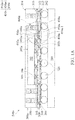
- FIG. 1A is a cross-sectional view of a semiconductor package assembly 500a including a system-on-chip (SOC) package in accordance with some embodiments of the disclosure.
- FIG. 1B is an enlarged view of a portion 600a of FIG. 1A , showing a metal-insulator-metal (MIM) capacitor structure 450a embedded in a redistribution layer (RDL) structure 308.
- the semiconductor package assembly 500a is a wafer-level semiconductor package assembly, for example, a flip-chip semiconductor package assembly.
- the semiconductor package assembly 500a includes at least one wafer-level semiconductor package mounted on a base 200.
- the wafer-level semiconductor package 300a includes a system-on-chip (SOC) package.
- the base 200 for example a printed circuit board (PCB), may be formed of polypropylene (PP). It should also be noted that the base 200 can be a single layer or a multilayer structure.
- a plurality of pads (not shown) and/or conductive traces (not shown) is disposed on a die-attach surface 202 of the base 200.
- the conductive traces may comprise power segments, signal trace segments or ground trace segments, which are used for the input/output (I/O) connections of the semiconductor package 300a.
- the semiconductor package 300a is mounted directly on the conductive traces. In some other embodiments, the pads are disposed on the die-attach surface 202, connected to different terminals of the conductive traces. The pads are used for the semiconductor package 300a mounted directly thereon.
- the semiconductor package 300a is mounted on the die-attach surface 202 of the base 200 by a bonding process.
- the semiconductor package 300a is mounted on the base 200 through the conductive structures 320.
- the semiconductor package 300a includes a semiconductor die 302 and a redistribution layer (RDL) structure 308.
- the semiconductor die 302 may be a system-on-chip (SOC) die.
- the semiconductor die 302 for example, may include a logic die including a central processing unit (CPU), a graphics processing unit (GPU), a dynamic random access memory (DRAM) controller or any combination thereof.
- the semiconductor die 302 is fabricated by flip-chip technology.
- Pads 304 of the semiconductor die 302 are disposed on a front surface 302b to be electrically connected to the circuitry (not shown) of the semiconductor die 302.
- the pads 304 belong to the uppermost metal layer of the interconnection structure (not shown) of the semiconductor die 302.
- the pads 304 of the semiconductor die 302 are in contact with the corresponding conductive structures 306, for example, conductive bumps. It should be noted that the number of semiconductor dies 302 integrated in the semiconductor package assembly 500a is not limited to that disclosed in the embodiment.
- the semiconductor package 300a further includes a molding compound 350 covering and surrounding the semiconductor die 302.
- the molding compound 350 is in contact with the semiconductor die 302.
- the molding compound 350 has opposite surfaces 352 and 354 that are respectively close to the front surface 302b and back surface 302a of the semiconductor die 302.
- the molding compound 350 may also cover the back surface 302a of the semiconductor die 302.
- the molding compound 350 may be formed of a nonconductive material, such as an epoxy, a resin, a moldable polymer, or the like.
- the molding compound 350 may be applied while substantially liquid, and then may be cured through a chemical reaction, such as in an epoxy or resin.
- the molding compound 350 may be an ultraviolet (UV) or thermally cured polymer applied as a gel or malleable solid capable of being disposed around the semiconductor die 302, and then may be cured through a UV or thermal curing process.
- the molding compound 350 may be cured with a mold (not shown).
- the semiconductor package 300a further includes the redistribution layer (RDL) structure 308 disposed over the front surface 302b of the semiconductor die 302.
- the RDL structure 308 is also disposed on the surface 352 of the molding compound 350.
- the semiconductor die 302 of the semiconductor package 300a is connected to a surface 310 of the RDL structure 308 through conductive structures 306, for example, conductive bumps or solder pastes.
- the RDL structure 308 may be in contact with the molding compound 350.
- the RDL structure 308 may have one or more conductive traces 314 (comprising a first conductive trace 452a and a second conductive trace 454a) disposed in one or more inter-metal dielectric (IMD) layers 318. Pad portions of the conductive traces 314 are exposed to openings of the solder mask layer 316.
- IMD inter-metal dielectric
- the RDL structure 308 of the semiconductor package 300a further includes a metal-insulator-metal (MIM) capacitor structure 450a embedded therein.
- the MIM capacitor structure 450a is coupled to the semiconductor die 302.
- the MIM capacitor structure 450a includes a first electrode 452a-1, a second electrode 454a-1 and an inter-metal dielectric (IMD) layer 456a therebetween.
- the first electrode 452a-1 is a segment of a first conductive trace 452a of the RDL structure 308, which is close to the SOC die 302.
- the second electrode 454a-1 is a segment of a second conductive trace 454a of the RDL structure 308, which is close to the conductive structures 320.
- the first conductive trace 452a is designed to be positioned at a first layer-level
- the second conductive trace 454a is designed to be positioned at a second layer-level different from the first layer-level.
- the first conductive trace 452a is separated from the second conductive trace 454a through the inter-metal dielectric (IMD) layers 318 and 456a.
- IMD inter-metal dielectric
- the first electrode 452a-1 is substantially parallel to the second electrode 454a-1.
- the first electrode 452a-1 and the second electrode 454a-1 of the MIM capacitor structure 450a are strip shape in a cross-sectional view.
- each of the first electrode 452a-1 and the second electrode 454a-1 has an even surface in the cross-sectional view as shown in FIGS. 1A and 1B .
- the first conductive trace 452a and the first electrode 452a-1 are designed to have a uniform thickness T1.
- the second conductive trace 454a and the second electrode 454a-1 are designed to have a uniform thickness T2.
- the thickness T1 is substantially equal to the thickness T2.
- the thickness T1 and the thickness T2 are designed to be lower than or equal to 4 ⁇ m.
- the IMD layer 456a of the MIM capacitor structure 450a is disposed beside the IMD layer 318, which is between the first conductive trace 452a and the second conductive trace 454a.
- the IMD layer 456a is strip shape in a cross-sectional view.
- an interface 458a between the first electrode 452a-1 and the IMD layer 456a, or an interface 460a between the second electrode 454a-1 and the IMD layer 456a is substantially an even surface in the cross-sectional view as shown in FIGS. 1A and 1B .
- the IMD layer 456a is a high-k dielectric layer (k is the dielectric constant of the dielectric layer).
- the dielectric constant of the IMD layer 318 is five times lower than the dielectric constant of the IMD layer 456a.
- the IMD layer 456a may be formed of organic materials, which include a polymer base material, non-organic materials, which include silicon nitride (SiN X ), silicon oxide (SiO X ), grapheme, or the like.
- the IMD layer 456a may be formed of a photo sensitive material, which includes a dry film photoresist, or a taping film.
- the thickness T3 of the IMD layer 456a of the MIM capacitor structure 450a is designed to be less than the thickness T4 of the IMD layer 318. Also, the thickness T3 of the IMD layer 456a is designed to be less than or equal to the thickness T1 of the first conductive trace 452a and the thickness T2 of the second conductive trace 454a in the cross-sectional view as shown in FIG. 1B . For example, the thickness T3 of the IMD layer 456a of the MIM capacitor structure 450a is designed to be less than or equal to about 4 ⁇ m.
- the semiconductor package 300a further includes vias 322 passing through the molding compound 350.
- the vias 322 are coupled to the conductive traces 314 (comprising a first conductive trace 452a and a second conductive trace 454a) of the RDL structure 308.
- the semiconductor die 302 is surrounded by the vias 322. Two terminals of each of the vias 322 are respectively close to the surface 310 of the RDL structure 308 and the surface 354 of the molding compound 350.
- the vias 322 may comprise through package vias (TPVs) formed of copper.
- the semiconductor package 300a further includes conductive structures 320 disposed on a surface 312 of the RDL structure 308, which is away from the semiconductor die 302.
- the conductive structures 320 are coupled to the conductive traces 314 through the exposed to openings of the solder mask layer 316.
- the conductive structures 320 are separated from the molding compound 350 through the RDL structure 308.
- the conductive structures 320 are free from contact with the molding compound 350.
- the conductive structures 320 may comprise a conductive bump structure such as a copper bump or a solder bump structure, a conductive pillar structure, a conductive wire structure, or a conductive paste structure.
- the semiconductor package assembly 500a is designed to fabricate a passive device structure, for example, a metal-insulator-metal (MIM) capacitor structure 450a embedded in a redistribution layer (RDL) structure 308.
- MIM capacitor structure 450a is composed segments of conductive traces (the first electrode 452a-1 and the second electrode 454a-1) of the RDL structure 308 and a high-k capacitor dielectric material layer (the IMD layer 456a) beside the IMD layer (the IMD layer 318) of the RDL structure 308.
- the capacitor structure 450a is designed to increase the dielectric constant (k) of the IMD layer 456a, or to decrease the thicknesses of the first electrode 452a-1 (the thickness T1), the second electrode 454a-1 (the thickness T2) and the IMD layer 456a (the thickness T3), so that the larger capacitance value is obtained.
- the embedded MIM capacitor structure 450a can be integrated with the RDL structure 308 and using a process similar to the fabrication process of the RDL structure 308.
- the MIM capacitor structure 450a may provide comparable process capability in the semiconductor package assembly.
- the semiconductor package assembly 500a may help to improve the surface-mount technology (SMT) yield even when the semiconductor die (the SOC die 302) is replaced.
- the signal integrity/power integrity (SI/PI) performance of the embedded MIM capacitor structure 450a can be improved due to the shortened routing path between the semiconductor die (the SOC die 302) and the MIM capacitor structure 450a.
- the embedded MIM capacitor structure 450a can provide design flexibility for the system integration of the semiconductor package assembly 500a.
- FIG. 2A is a cross-sectional view of a semiconductor package assembly 500b including a system-on-chip (SOC) package in accordance with some embodiments of the disclosure.
- FIG. 2B is an enlarged view of a portion 600b of FIG. 2A , showing a metal-insulator-metal (MIM) capacitor structure 450b embedded in a redistribution layer (RDL) structure 308.
- MIM metal-insulator-metal
- RDL redistribution layer
- the semiconductor package assembly 500b includes the MIM capacitor structure 450b embedded in the RDL structure 308 of a system-on-chip (SOC) package 300b.
- the MIM capacitor structure 450b includes a first electrode 452b-1, a second electrode 454b-1 and an inter-metal dielectric (IMD) layer 456b therebetween.
- the first electrode 452b-1 is a segment of a first conductive trace 452b of the RDL structure 308, which is close to the semiconductor die 302.
- the second electrode 454b-1 is a segment of a second conductive trace 454b of the RDL structure 308, which is close to the conductive structures 320.
- the first conductive trace 452b is designed to be positioned at a first layer-level
- the second conductive trace 454b is designed to be positioned at a second layer-level different from the first layer-level.
- the first conductive trace 452b is separated from the second conductive trace 454b through the inter-metal dielectric (IMD) layers 318 and 456b.
- the first conductive trace 452b is designed to have a uniform thickness T1.
- the second conductive trace 454b is designed to have a uniform thickness T2.
- the thickness T1 is substantially equal to the thickness T2.
- the thickness T1 and the thickness T2 are designed to be less than or equal to 4 ⁇ m.
- the first electrode 452b-1 is substantially parallel to the second electrode 454b-1.
- the first electrode 452b-1 and the second electrode 454b-1 of the MIM capacitor structure 450b are zigzag shapes in a cross-sectional view.
- the first electrode 452b-1 has an uneven surface including convex portions 452b-1a and concave portions 452b-1b in the cross-sectional view as shown in FIG. 2B .
- the second electrode 454b-1 has an uneven surface including convex portions 454b-1a and concave portions 454b-1b in the cross-sectional view as shown in FIG. 2B .
- the IMD layer 456b of the MIM capacitor structure 450b is disposed beside the IMD layer 318, which is between the first conductive trace 452b and the second conductive trace 454b.
- the IMD layer 456a is a zigzag shape in a cross-sectional view.
- the first electrode 452b-1 and the second electrode 454b-1 of the MIM capacitor structure 450b, which are in contact with the IMD layer 456b, are zigzag shape in the cross-sectional view as shown in FIGS. 2A and 2B .
- an interface 458b between the first electrode 452b-1 and the IMD layer 456a, or an interface 460b between the second electrode 454b-1 and the IMD layer 456b is substantially an uneven and periodically varying surface in the cross-sectional view as shown in FIGS. 2A and 2B .
- the interface 458b has an uneven surface including convex portions corresponding to the convex portions 452b-1a and concave portions corresponding to the concave portions 452b-1b.
- the interface 460b has an uneven surface including convex portions corresponding to the convex portions 454b-1a and concave portions corresponding to the concave portions 454b-1b.
- the thickness T3 of the IMD layer 456b of the MIM capacitor structure 450b is designed to be less than the thickness T4 of the IMD layer 318. Also, the thickness T3 of the IMD layer 456b is designed to be less than or equal to the thickness T1 of the first conductive trace 452b and the thickness T2 of the second conductive trace 454b in the cross-sectional view as shown in FIG. 2B . For example, the thickness T3 of the IMD layer 456b of the MIM capacitor structure 450b is designed to be less than or equal to about 4 ⁇ m.
- the semiconductor package assembly 500b is designed to fabricate a passive device structure, for example, a metal-insulator-metal (MIM) capacitor structure 450b embedded in a redistribution layer (RDL) structure 308 of the semiconductor package 300b.
- MIM metal-insulator-metal
- RDL redistribution layer
- the capacitor structure 450b is designed to have zigzag-shaped electrodes (the first electrode 452b-1 and the second electrode 454b-1) and a zigzag-shaped capacitor dielectric layer (the IMD layer 456b) to increase the area of the capacitor structure 450b, so that the larger capacitance value is obtained.
- the capacitor structure 450b is designed to increase the dielectric constant (k) of the IMD layer 456b, or to decrease the thicknesses of the first electrode 452b-1 (the thickness T1), the second electrode 454b-1 (the thickness T2) and the IMD layer 456b (the thickness T3) to obtain the larger capacitance value.
- FIG. 3 is a cross-sectional view of a semiconductor package assembly 500c including a semiconductor package 300c in accordance with some embodiments of the disclosure. Descriptions of elements of the embodiments hereinafter that are the same or similar as those previously described with reference to FIGS. 1A-1B and 2A-2B are omitted for brevity.
- a semiconductor package 300c of the semiconductor package assembly 500c includes two semiconductor dies 202a and 202b arranged side-by-side.
- at least one of the semiconductor dies 202a and 202b is a system on chip (SOC) die.
- the semiconductor dies 202a and 202b are SOC die.
- the semiconductor die 202a is a SOC die
- the semiconductor dies 202b is a memory die, such as a dynamic random access memory (DRAM) die.
- DRAM dynamic random access memory
- the MIM capacitor structure 450b embedded in the RDL structure 308 is designed to be coupled to the SOC die (semiconductor die 202a). Therefore, the semiconductor package 300c of the semiconductor package assembly 500c includes a pure SOC package or a hybrid SOC package. However, the number and the arrangement of semiconductor dies are not limited to the disclosed embodiment.
- FIG. 4 is a cross-sectional view of a semiconductor package assembly 500d including a first semiconductor package 300d and a second semiconductor package 400, for example, a dynamic random access memory (DRAM) package, stacked thereon in accordance with some embodiments of the disclosure.
- DRAM dynamic random access memory
- a first semiconductor package 300d of the semiconductor package assembly 500d further includes a second redistribution layer (RDL) structure 328 disposed on the first semiconductor die 302.
- the semiconductor package assembly 500d further includes an second semiconductor package 400 stacked on the semiconductor package 300d by a bonding process.
- the RDL structure 328 is disposed on the molding compound 350.
- a surface 324 of the RDL structure 328, which is close to the first semiconductor die 302, is in contact with the surface 354 of the molding compound 350.
- the opposite surfaces 352 and 354 of the molding compound 350 are in contact with the RDL structures 308 and 328, respectively.
- the RDL structure 328 may have one or more conductive traces 336 disposed in one or more inter-metal dielectric (IMD) layers 334. Pad portions of the conductive traces 336 are exposed to openings of one the IMD layers 334, which is away from the surface 354 of the molding compound 350.
- IMD inter-metal dielectric
- the number of conductive traces 336 and the number of IMD layers 328 shown in FIG. 4 is only an example and is not a limitation to the present invention.
- the RDL structure 328 is coupled to the RDL structure 308 by vias 322 passing through the molding compound 350 between the RDL structure 308 and the RDL structure 328.
- the semiconductor package assembly 500d further includes the second semiconductor package 400 stacked on the first semiconductor package 300d.
- the second semiconductor package 400 includes a memory package, for example, a dynamic random access memory (DRAM) package.
- the second semiconductor package 400 is mounted on the first semiconductor package 300 through the conductive structures 428.
- the second semiconductor package 400 is coupled to the RDL structure 308 of the by the RDL structure 328 and the vias 322 of the first semiconductor package 300d.
- DRAM dynamic random access memory
- the second semiconductor package 400 comprises a redistribution layer (RDL) structure 418, at least one semiconductor die (e.g. two DRAM dies 402 and 404) and a molding compound 412. Because the second semiconductor package 400 is stacked on the first semiconductor package 300d, the RDL structure 328 is positioned between the RDL structure 308 and 418.
- the RDL structure 418 has opposite surface 420 and 422. The surface 420 is provided for semiconductor dies mounted thereon, and the surface 422 is provided for conductive bumps 428 attached thereon.
- the RDL structure 418 may have one or more conductive traces 426 disposed in one or more inter-metal dielectric (IMD) layers 424.
- IMD inter-metal dielectric
- Pad portions of the conductive traces 426 are exposed to openings of a solder mask layer 427.
- the number of conductive traces 426 and the number of IMD layers 424 shown in FIG. 4 is only an example and is not a limitation of the present invention
- the semiconductor dies 402 and 404 are DRAM dies.
- the semiconductor die 402 is mounted on the surface 420 of the RDL structure 418 with a paste (not shown).
- the semiconductor die 404 is stacked on the semiconductor die 402 with a paste (not shown).
- the semiconductor die 402 has pads 408 thereon, and the semiconductor die 404 has pads 410 thereon.
- the pads 408 and 410 of the semiconductor dies 402 and 404 may be coupled to pads 425 of the RDL structure 418 by bonding wires, for example bonding wires 414 and 416, respectively.
- bonding wires for example bonding wires 414 and 416, respectively.
- the number of stacked semiconductor dies is not limited to the disclosed embodiment.
- the two semiconductor dies 402 and 404 shown in FIG. 4 can be arranged side by side. Therefore, the semiconductor dies 402 and 404 are mounted on the surface 420 of the RDL structure 418 by a paste (not shown).
- molding compound 412 surrounds the semiconductor dies 402 and 404. Also, the molding compound 412 is in contact with the surface 420 of the RDL structure 412 and the semiconductor dies 402 and 404. Like molding compound 350, molding compound 412 may be formed of a nonconductive material, such as an epoxy, a resin, a moldable polymer, or the like.
- the second semiconductor package 400 further includes conductive structures 428 disposed on the surface 422 of the RDL structure 418, which is away from the semiconductor dies 402 and 404.
- the conductive structures 428 are formed through the openings of the solder mask layer 427 to couple to the conductive traces 424. Also, the conductive structures 428 are separated from the molding compound 412 through the RDL structure 418.
- the second semiconductor package 400 is coupled to the RDL structure 308 and/or the MIM capacitor structure 450b of the first semiconductor package 300d. More specifically, the conductive structures 428 of the second semiconductor package 400 are coupled to vias 340 formed through the RDL structure 328 of the first semiconductor package 300d.
- conductive structures 428 may comprise a conductive bump structure such as a copper bump or a solder bump structure, a conductive pillar structure, a conductive wire structure, or a conductive paste structure.
- the semiconductor die 302 can be a baseband chip, another semiconductor 402 or 404 can be a RF (radio-frequency) chip.
- the semiconductor die 302 can be a AP (analog processor) chip, another semiconductor die 402 or 404 can be a DP (digital processor) chip.
- Embodiments provide a semiconductor package assembly.
- the semiconductor package assembly is designed to fabricate a passive device structure, for example, a metal-insulator-metal (MIM) capacitor structure embedded in and integrated with a redistribution layer (RDL) structure.
- MIM capacitor structure is composed segments of conductive traces (serving as the first electrode and the second electrode) of the RDL structure and a high-k capacitor dielectric material layer (k ⁇ 20) beside the low-k IMD layer (k ⁇ 4) of the RDL structure.
- the capacitor structure is designed to increase the dielectric constant (k) of the high-k capacitor dielectric material layer, or to decrease the thicknesses of the first electrode, the second electrode and the high-k capacitor dielectric material layer, so that the larger capacitance value is obtained.
- the capacitor structure is designed to have zigzag-shaped electrodes and a zigzag-shaped capacitor dielectric layer to increase the area of the capacitor structure, thereby increasing the capacitance value.
- the fabrication process of embedded MIM capacitor structure can be integrated with that of the RDL structure. Therefore, the MIM capacitor structure may provide the comparable process capability. Therefore, the MIM capacitor structure may provide the comparable process capability.
- the semiconductor package assembly may help to improve the surface-mount technology (SMT) yield even when the semiconductor die (the SOC die) is replaced. Additionally, the signal integrity/power integrity (SI/PI) performance of the embedded MIM capacitor structure can be improved due to the shortened routing path between the semiconductor die (the SOC die) and the MIM capacitor structure.
- the embedded MIM capacitor structure can provide the design flexibility for the system integration of the semiconductor package assembly.
Landscapes
- Semiconductor Integrated Circuits (AREA)
- Engineering & Computer Science (AREA)
- Manufacturing & Machinery (AREA)
- Production Of Multi-Layered Print Wiring Board (AREA)
- Power Engineering (AREA)
- Physics & Mathematics (AREA)
- Geometry (AREA)
Applications Claiming Priority (2)
| Application Number | Priority Date | Filing Date | Title |
|---|---|---|---|
| US201562133680P | 2015-03-16 | 2015-03-16 | |
| US15/014,636 US9704836B2 (en) | 2015-03-16 | 2016-02-03 | Semiconductor package assembly |
Publications (3)
| Publication Number | Publication Date |
|---|---|
| EP3073525A2 true EP3073525A2 (de) | 2016-09-28 |
| EP3073525A3 EP3073525A3 (de) | 2016-12-21 |
| EP3073525B1 EP3073525B1 (de) | 2020-08-05 |
Family
ID=55524178
Family Applications (1)
| Application Number | Title | Priority Date | Filing Date |
|---|---|---|---|
| EP16159135.9A Active EP3073525B1 (de) | 2015-03-16 | 2016-03-08 | Halbleitergehäuseanordnung |
Country Status (4)
| Country | Link |
|---|---|
| US (2) | US9704836B2 (de) |
| EP (1) | EP3073525B1 (de) |
| CN (1) | CN105990293A (de) |
| TW (1) | TWI615941B (de) |
Families Citing this family (22)
| Publication number | Priority date | Publication date | Assignee | Title |
|---|---|---|---|---|
| US10460987B2 (en) * | 2017-05-09 | 2019-10-29 | Taiwan Semiconductor Manufacturing Company Ltd. | Semiconductor package device with integrated antenna and manufacturing method thereof |
| US10475735B2 (en) | 2017-06-15 | 2019-11-12 | Applied Materials, Inc. | Methods and apparatus for 3D MIM capacitor package processing |
| US10763242B2 (en) | 2017-06-23 | 2020-09-01 | Samsung Electronics Co., Ltd. | Semiconductor package and method of manufacturing the same |
| US20190006457A1 (en) * | 2017-06-29 | 2019-01-03 | Intel Corporation | Package integrated passives |
| KR102385549B1 (ko) * | 2017-08-16 | 2022-04-12 | 삼성전자주식회사 | 반도체 패키지 및 반도체 패키지의 제조 방법 |
| US10504865B2 (en) * | 2017-09-28 | 2019-12-10 | Taiwan Semiconductor Manufacturing Co., Ltd. | Package structure and method of manufacturing the same |
| KR102381197B1 (ko) | 2017-12-08 | 2022-04-01 | 삼성전자주식회사 | 반도체 소자 |
| TWI659515B (zh) * | 2018-07-26 | 2019-05-11 | 欣興電子股份有限公司 | 封裝結構及其製造方法 |
| US11088095B2 (en) * | 2018-12-07 | 2021-08-10 | Nanya Technology Corporation | Package structure |
| US10867966B2 (en) * | 2019-04-29 | 2020-12-15 | Taiwan Semiconductor Manufacturing Company, Ltd. | Package structure, package-on-package structure and method of fabricating the same |
| US11189686B2 (en) * | 2019-09-30 | 2021-11-30 | Qualcomm Incorporated | Integrated device coupled to a capacitor structure comprising a trench capacitor |
| CN115104179A (zh) * | 2020-03-02 | 2022-09-23 | 华为技术有限公司 | 封装结构及封装结构的制作方法 |
| US11158590B1 (en) * | 2020-04-23 | 2021-10-26 | Qualcomm Incorporated | Capacitor interposer layer (CIL) in a die-to-wafer three-dimensional (3D) integrated circuit (IC) (3DIC) |
| US11538748B2 (en) | 2020-06-04 | 2022-12-27 | Mediatek Singapore Pte. Ltd. | Semiconductor device with capacitor element |
| CN114975129A (zh) * | 2021-02-26 | 2022-08-30 | 诺思(天津)微系统有限责任公司 | 集成电路封装结构及隔离度提高方法和多工器与通信设备 |
| TWI787805B (zh) * | 2021-05-04 | 2022-12-21 | 矽品精密工業股份有限公司 | 電子模組及其製法與電子封裝件 |
| US20220392855A1 (en) * | 2021-06-08 | 2022-12-08 | Intel Corporation | Microelectronic assemblies having integrated thin film capacitors |
| US20230011666A1 (en) * | 2021-07-09 | 2023-01-12 | Mediatek Singapore Pte. Ltd. | Semiconductor package structure |
| US20230197697A1 (en) * | 2021-12-16 | 2023-06-22 | Intel Corporation | Microelectronic assemblies with glass substrates and thin film capacitors |
| US20240113158A1 (en) * | 2022-09-30 | 2024-04-04 | Intel Corporation | High surface area capacitor in an electronic substrate package |
| US12588291B2 (en) * | 2023-06-13 | 2026-03-24 | Intel Corporation | Substrates including micro-structured thin film capacitors |
| EP4723863A1 (de) * | 2024-10-01 | 2026-04-08 | Samsung Electronics Co., Ltd. | Halbleiteranordnung mit integriertem stapelkondensator und verfahren zu deren herstellung |
Family Cites Families (20)
| Publication number | Priority date | Publication date | Assignee | Title |
|---|---|---|---|---|
| KR100471164B1 (ko) * | 2002-03-26 | 2005-03-09 | 삼성전자주식회사 | 금속-절연체-금속 캐패시터를 갖는 반도체장치 및 그제조방법 |
| TWI234253B (en) | 2002-05-31 | 2005-06-11 | Fujitsu Ltd | Semiconductor device and manufacturing method thereof |
| JP4736451B2 (ja) * | 2005-02-03 | 2011-07-27 | パナソニック株式会社 | 多層配線基板とその製造方法、および多層配線基板を用いた半導体パッケージと電子機器 |
| US7528474B2 (en) * | 2005-05-31 | 2009-05-05 | Stats Chippac Ltd. | Stacked semiconductor package assembly having hollowed substrate |
| US20070080458A1 (en) * | 2005-10-11 | 2007-04-12 | Tsuyoshi Ogawa | Hybrid module and method of manufacturing the same |
| US8072059B2 (en) | 2006-04-19 | 2011-12-06 | Stats Chippac, Ltd. | Semiconductor device and method of forming UBM fixed relative to interconnect structure for alignment of semiconductor die |
| US7964961B2 (en) * | 2007-04-12 | 2011-06-21 | Megica Corporation | Chip package |
| US8039303B2 (en) | 2008-06-11 | 2011-10-18 | Stats Chippac, Ltd. | Method of forming stress relief layer between die and interconnect structure |
| US7858441B2 (en) * | 2008-12-08 | 2010-12-28 | Stats Chippac, Ltd. | Semiconductor package with semiconductor core structure and method of forming same |
| US20100224960A1 (en) | 2009-03-04 | 2010-09-09 | Kevin John Fischer | Embedded capacitor device and methods of fabrication |
| US8164158B2 (en) * | 2009-09-11 | 2012-04-24 | Stats Chippac, Ltd. | Semiconductor device and method of forming integrated passive device |
| US8624353B2 (en) | 2010-12-22 | 2014-01-07 | Stats Chippac, Ltd. | Semiconductor device and method of forming integrated passive device over semiconductor die with conductive bridge and fan-out redistribution layer |
| US8748284B2 (en) * | 2011-08-12 | 2014-06-10 | Taiwan Semiconductor Manufacturing Company, Ltd. | Method of manufacturing decoupling MIM capacitor designs for interposers |
| US9960106B2 (en) | 2012-05-18 | 2018-05-01 | Taiwan Semiconductor Manufacturing Co., Ltd. | Package with metal-insulator-metal capacitor and method of manufacturing the same |
| US9378982B2 (en) | 2013-01-31 | 2016-06-28 | Taiwan Semiconductor Manufacturing Company, Ltd. | Die package with openings surrounding end-portions of through package vias (TPVs) and package on package (PoP) using the die package |
| US9048222B2 (en) | 2013-03-06 | 2015-06-02 | Taiwan Semiconductor Manufacturing Company, Ltd. | Method of fabricating interconnect structure for package-on-package devices |
| US9577025B2 (en) * | 2014-01-31 | 2017-02-21 | Qualcomm Incorporated | Metal-insulator-metal (MIM) capacitor in redistribution layer (RDL) of an integrated device |
| US9343434B2 (en) * | 2014-02-27 | 2016-05-17 | Taiwan Semiconductor Manufacturing Company, Ltd. | Laser marking in packages |
| US9281297B2 (en) * | 2014-03-07 | 2016-03-08 | Taiwan Semiconductor Manufacturing Company, Ltd. | Solution for reducing poor contact in info packages |
| US9704796B1 (en) * | 2016-02-11 | 2017-07-11 | Qualcomm Incorporated | Integrated device comprising a capacitor that includes multiple pins and at least one pin that traverses a plate of the capacitor |
-
2016
- 2016-02-03 US US15/014,636 patent/US9704836B2/en active Active
- 2016-03-08 EP EP16159135.9A patent/EP3073525B1/de active Active
- 2016-03-15 CN CN201610146169.7A patent/CN105990293A/zh active Pending
- 2016-03-15 TW TW105107875A patent/TWI615941B/zh not_active IP Right Cessation
-
2017
- 2017-06-09 US US15/618,210 patent/US10177125B2/en active Active
Non-Patent Citations (1)
| Title |
|---|
| None |
Also Published As
| Publication number | Publication date |
|---|---|
| US9704836B2 (en) | 2017-07-11 |
| US20170278832A1 (en) | 2017-09-28 |
| TW201705442A (zh) | 2017-02-01 |
| TWI615941B (zh) | 2018-02-21 |
| US10177125B2 (en) | 2019-01-08 |
| EP3073525A3 (de) | 2016-12-21 |
| US20160276324A1 (en) | 2016-09-22 |
| CN105990293A (zh) | 2016-10-05 |
| EP3073525B1 (de) | 2020-08-05 |
Similar Documents
| Publication | Publication Date | Title |
|---|---|---|
| EP3073525B1 (de) | Halbleitergehäuseanordnung | |
| US10217724B2 (en) | Semiconductor package assembly with embedded IPD | |
| US11728292B2 (en) | Semiconductor package assembly having a conductive electromagnetic shield layer | |
| US11574881B2 (en) | Semiconductor package structure with antenna | |
| US9978729B2 (en) | Semiconductor package assembly | |
| US20190252351A1 (en) | Semiconductor package structure having an antenna pattern electrically coupled to a first redistribution layer (rdl) | |
| US10483211B2 (en) | Fan-out package structure and method for forming the same | |
| US10424563B2 (en) | Semiconductor package assembly and method for forming the same | |
| US11469208B2 (en) | Method of manufacturing semiconductor package structure | |
| US20140367850A1 (en) | Stacked package and method of fabricating the same | |
| US9997498B2 (en) | Semiconductor package assembly | |
| US10147674B2 (en) | Semiconductor package assembly | |
| US20210035930A1 (en) | Semiconductor package structure including antenna |
Legal Events
| Date | Code | Title | Description |
|---|---|---|---|
| PUAI | Public reference made under article 153(3) epc to a published international application that has entered the european phase |
Free format text: ORIGINAL CODE: 0009012 |
|
| AK | Designated contracting states |
Kind code of ref document: A2 Designated state(s): AL AT BE BG CH CY CZ DE DK EE ES FI FR GB GR HR HU IE IS IT LI LT LU LV MC MK MT NL NO PL PT RO RS SE SI SK SM TR |
|
| AX | Request for extension of the european patent |
Extension state: BA ME |
|
| PUAL | Search report despatched |
Free format text: ORIGINAL CODE: 0009013 |
|
| AK | Designated contracting states |
Kind code of ref document: A3 Designated state(s): AL AT BE BG CH CY CZ DE DK EE ES FI FR GB GR HR HU IE IS IT LI LT LU LV MC MK MT NL NO PL PT RO RS SE SI SK SM TR |
|
| AX | Request for extension of the european patent |
Extension state: BA ME |
|
| RIC1 | Information provided on ipc code assigned before grant |
Ipc: H01L 25/10 20060101ALN20161117BHEP Ipc: H01L 23/522 20060101AFI20161117BHEP Ipc: H01L 23/538 20060101ALI20161117BHEP Ipc: H01L 23/498 20060101ALI20161117BHEP Ipc: H01L 25/065 20060101ALN20161117BHEP Ipc: H01L 25/16 20060101ALI20161117BHEP |
|
| STAA | Information on the status of an ep patent application or granted ep patent |
Free format text: STATUS: REQUEST FOR EXAMINATION WAS MADE |
|
| 17P | Request for examination filed |
Effective date: 20170601 |
|
| RBV | Designated contracting states (corrected) |
Designated state(s): AL AT BE BG CH CY CZ DE DK EE ES FI FR GB GR HR HU IE IS IT LI LT LU LV MC MK MT NL NO PL PT RO RS SE SI SK SM TR |
|
| STAA | Information on the status of an ep patent application or granted ep patent |
Free format text: STATUS: EXAMINATION IS IN PROGRESS |
|
| 17Q | First examination report despatched |
Effective date: 20190509 |
|
| RIC1 | Information provided on ipc code assigned before grant |
Ipc: H01L 25/065 20060101ALN20191217BHEP Ipc: H01L 25/10 20060101ALN20191217BHEP Ipc: H01L 25/16 20060101ALI20191217BHEP Ipc: H01L 23/522 20060101AFI20191217BHEP Ipc: H01L 23/498 20060101ALI20191217BHEP Ipc: H01L 23/538 20060101ALI20191217BHEP |
|
| GRAP | Despatch of communication of intention to grant a patent |
Free format text: ORIGINAL CODE: EPIDOSNIGR1 |
|
| STAA | Information on the status of an ep patent application or granted ep patent |
Free format text: STATUS: GRANT OF PATENT IS INTENDED |
|
| RIC1 | Information provided on ipc code assigned before grant |
Ipc: H01L 23/522 20060101AFI20200121BHEP Ipc: H01L 25/16 20060101ALI20200121BHEP Ipc: H01L 23/538 20060101ALI20200121BHEP Ipc: H01L 25/10 20060101ALN20200121BHEP Ipc: H01L 25/065 20060101ALN20200121BHEP Ipc: H01L 23/498 20060101ALI20200121BHEP |
|
| RIN1 | Information on inventor provided before grant (corrected) |
Inventor name: PENG, I-HSUAN Inventor name: LIN, TZU-HUNG Inventor name: HSIAO, CHING-WEN |
|
| INTG | Intention to grant announced |
Effective date: 20200212 |
|
| GRAJ | Information related to disapproval of communication of intention to grant by the applicant or resumption of examination proceedings by the epo deleted |
Free format text: ORIGINAL CODE: EPIDOSDIGR1 |
|
| STAA | Information on the status of an ep patent application or granted ep patent |
Free format text: STATUS: EXAMINATION IS IN PROGRESS |
|
| GRAR | Information related to intention to grant a patent recorded |
Free format text: ORIGINAL CODE: EPIDOSNIGR71 |
|
| GRAS | Grant fee paid |
Free format text: ORIGINAL CODE: EPIDOSNIGR3 |
|
| STAA | Information on the status of an ep patent application or granted ep patent |
Free format text: STATUS: GRANT OF PATENT IS INTENDED |
|
| GRAA | (expected) grant |
Free format text: ORIGINAL CODE: 0009210 |
|
| STAA | Information on the status of an ep patent application or granted ep patent |
Free format text: STATUS: THE PATENT HAS BEEN GRANTED |
|
| INTC | Intention to grant announced (deleted) | ||
| RIC1 | Information provided on ipc code assigned before grant |
Ipc: H01L 25/065 20060101ALN20200617BHEP Ipc: H01L 23/498 20060101ALI20200617BHEP Ipc: H01L 25/10 20060101ALN20200617BHEP Ipc: H01L 25/16 20060101ALI20200617BHEP Ipc: H01L 23/522 20060101AFI20200617BHEP Ipc: H01L 23/538 20060101ALI20200617BHEP |
|
| AK | Designated contracting states |
Kind code of ref document: B1 Designated state(s): AL AT BE BG CH CY CZ DE DK EE ES FI FR GB GR HR HU IE IS IT LI LT LU LV MC MK MT NL NO PL PT RO RS SE SI SK SM TR |
|
| INTG | Intention to grant announced |
Effective date: 20200629 |
|
| REG | Reference to a national code |
Ref country code: GB Ref legal event code: FG4D |
|
| REG | Reference to a national code |
Ref country code: CH Ref legal event code: EP |
|
| REG | Reference to a national code |
Ref country code: AT Ref legal event code: REF Ref document number: 1299929 Country of ref document: AT Kind code of ref document: T Effective date: 20200815 |
|
| REG | Reference to a national code |
Ref country code: DE Ref legal event code: R096 Ref document number: 602016041162 Country of ref document: DE |
|
| REG | Reference to a national code |
Ref country code: IE Ref legal event code: FG4D |
|
| REG | Reference to a national code |
Ref country code: LT Ref legal event code: MG4D |
|
| REG | Reference to a national code |
Ref country code: NL Ref legal event code: MP Effective date: 20200805 |
|
| REG | Reference to a national code |
Ref country code: AT Ref legal event code: MK05 Ref document number: 1299929 Country of ref document: AT Kind code of ref document: T Effective date: 20200805 |
|
| PG25 | Lapsed in a contracting state [announced via postgrant information from national office to epo] |
Ref country code: FI Free format text: LAPSE BECAUSE OF FAILURE TO SUBMIT A TRANSLATION OF THE DESCRIPTION OR TO PAY THE FEE WITHIN THE PRESCRIBED TIME-LIMIT Effective date: 20200805 Ref country code: HR Free format text: LAPSE BECAUSE OF FAILURE TO SUBMIT A TRANSLATION OF THE DESCRIPTION OR TO PAY THE FEE WITHIN THE PRESCRIBED TIME-LIMIT Effective date: 20200805 Ref country code: SE Free format text: LAPSE BECAUSE OF FAILURE TO SUBMIT A TRANSLATION OF THE DESCRIPTION OR TO PAY THE FEE WITHIN THE PRESCRIBED TIME-LIMIT Effective date: 20200805 Ref country code: NO Free format text: LAPSE BECAUSE OF FAILURE TO SUBMIT A TRANSLATION OF THE DESCRIPTION OR TO PAY THE FEE WITHIN THE PRESCRIBED TIME-LIMIT Effective date: 20201105 Ref country code: GR Free format text: LAPSE BECAUSE OF FAILURE TO SUBMIT A TRANSLATION OF THE DESCRIPTION OR TO PAY THE FEE WITHIN THE PRESCRIBED TIME-LIMIT Effective date: 20201106 Ref country code: ES Free format text: LAPSE BECAUSE OF FAILURE TO SUBMIT A TRANSLATION OF THE DESCRIPTION OR TO PAY THE FEE WITHIN THE PRESCRIBED TIME-LIMIT Effective date: 20200805 Ref country code: PT Free format text: LAPSE BECAUSE OF FAILURE TO SUBMIT A TRANSLATION OF THE DESCRIPTION OR TO PAY THE FEE WITHIN THE PRESCRIBED TIME-LIMIT Effective date: 20201207 Ref country code: AT Free format text: LAPSE BECAUSE OF FAILURE TO SUBMIT A TRANSLATION OF THE DESCRIPTION OR TO PAY THE FEE WITHIN THE PRESCRIBED TIME-LIMIT Effective date: 20200805 Ref country code: LT Free format text: LAPSE BECAUSE OF FAILURE TO SUBMIT A TRANSLATION OF THE DESCRIPTION OR TO PAY THE FEE WITHIN THE PRESCRIBED TIME-LIMIT Effective date: 20200805 Ref country code: BG Free format text: LAPSE BECAUSE OF FAILURE TO SUBMIT A TRANSLATION OF THE DESCRIPTION OR TO PAY THE FEE WITHIN THE PRESCRIBED TIME-LIMIT Effective date: 20201105 |
|
| PG25 | Lapsed in a contracting state [announced via postgrant information from national office to epo] |
Ref country code: PL Free format text: LAPSE BECAUSE OF FAILURE TO SUBMIT A TRANSLATION OF THE DESCRIPTION OR TO PAY THE FEE WITHIN THE PRESCRIBED TIME-LIMIT Effective date: 20200805 Ref country code: NL Free format text: LAPSE BECAUSE OF FAILURE TO SUBMIT A TRANSLATION OF THE DESCRIPTION OR TO PAY THE FEE WITHIN THE PRESCRIBED TIME-LIMIT Effective date: 20200805 Ref country code: LV Free format text: LAPSE BECAUSE OF FAILURE TO SUBMIT A TRANSLATION OF THE DESCRIPTION OR TO PAY THE FEE WITHIN THE PRESCRIBED TIME-LIMIT Effective date: 20200805 Ref country code: RS Free format text: LAPSE BECAUSE OF FAILURE TO SUBMIT A TRANSLATION OF THE DESCRIPTION OR TO PAY THE FEE WITHIN THE PRESCRIBED TIME-LIMIT Effective date: 20200805 Ref country code: IS Free format text: LAPSE BECAUSE OF FAILURE TO SUBMIT A TRANSLATION OF THE DESCRIPTION OR TO PAY THE FEE WITHIN THE PRESCRIBED TIME-LIMIT Effective date: 20201205 |
|
| PG25 | Lapsed in a contracting state [announced via postgrant information from national office to epo] |
Ref country code: RO Free format text: LAPSE BECAUSE OF FAILURE TO SUBMIT A TRANSLATION OF THE DESCRIPTION OR TO PAY THE FEE WITHIN THE PRESCRIBED TIME-LIMIT Effective date: 20200805 Ref country code: SM Free format text: LAPSE BECAUSE OF FAILURE TO SUBMIT A TRANSLATION OF THE DESCRIPTION OR TO PAY THE FEE WITHIN THE PRESCRIBED TIME-LIMIT Effective date: 20200805 Ref country code: EE Free format text: LAPSE BECAUSE OF FAILURE TO SUBMIT A TRANSLATION OF THE DESCRIPTION OR TO PAY THE FEE WITHIN THE PRESCRIBED TIME-LIMIT Effective date: 20200805 Ref country code: CZ Free format text: LAPSE BECAUSE OF FAILURE TO SUBMIT A TRANSLATION OF THE DESCRIPTION OR TO PAY THE FEE WITHIN THE PRESCRIBED TIME-LIMIT Effective date: 20200805 Ref country code: DK Free format text: LAPSE BECAUSE OF FAILURE TO SUBMIT A TRANSLATION OF THE DESCRIPTION OR TO PAY THE FEE WITHIN THE PRESCRIBED TIME-LIMIT Effective date: 20200805 |
|
| REG | Reference to a national code |
Ref country code: DE Ref legal event code: R097 Ref document number: 602016041162 Country of ref document: DE |
|
| PG25 | Lapsed in a contracting state [announced via postgrant information from national office to epo] |
Ref country code: AL Free format text: LAPSE BECAUSE OF FAILURE TO SUBMIT A TRANSLATION OF THE DESCRIPTION OR TO PAY THE FEE WITHIN THE PRESCRIBED TIME-LIMIT Effective date: 20200805 |
|
| PLBE | No opposition filed within time limit |
Free format text: ORIGINAL CODE: 0009261 |
|
| STAA | Information on the status of an ep patent application or granted ep patent |
Free format text: STATUS: NO OPPOSITION FILED WITHIN TIME LIMIT |
|
| PG25 | Lapsed in a contracting state [announced via postgrant information from national office to epo] |
Ref country code: SK Free format text: LAPSE BECAUSE OF FAILURE TO SUBMIT A TRANSLATION OF THE DESCRIPTION OR TO PAY THE FEE WITHIN THE PRESCRIBED TIME-LIMIT Effective date: 20200805 |
|
| 26N | No opposition filed |
Effective date: 20210507 |
|
| PG25 | Lapsed in a contracting state [announced via postgrant information from national office to epo] |
Ref country code: IT Free format text: LAPSE BECAUSE OF FAILURE TO SUBMIT A TRANSLATION OF THE DESCRIPTION OR TO PAY THE FEE WITHIN THE PRESCRIBED TIME-LIMIT Effective date: 20200805 |
|
| PG25 | Lapsed in a contracting state [announced via postgrant information from national office to epo] |
Ref country code: SI Free format text: LAPSE BECAUSE OF FAILURE TO SUBMIT A TRANSLATION OF THE DESCRIPTION OR TO PAY THE FEE WITHIN THE PRESCRIBED TIME-LIMIT Effective date: 20200805 |
|
| PG25 | Lapsed in a contracting state [announced via postgrant information from national office to epo] |
Ref country code: MC Free format text: LAPSE BECAUSE OF FAILURE TO SUBMIT A TRANSLATION OF THE DESCRIPTION OR TO PAY THE FEE WITHIN THE PRESCRIBED TIME-LIMIT Effective date: 20200805 |
|
| REG | Reference to a national code |
Ref country code: CH Ref legal event code: PL |
|
| REG | Reference to a national code |
Ref country code: BE Ref legal event code: MM Effective date: 20210331 |
|
| PG25 | Lapsed in a contracting state [announced via postgrant information from national office to epo] |
Ref country code: LI Free format text: LAPSE BECAUSE OF NON-PAYMENT OF DUE FEES Effective date: 20210331 Ref country code: LU Free format text: LAPSE BECAUSE OF NON-PAYMENT OF DUE FEES Effective date: 20210308 Ref country code: CH Free format text: LAPSE BECAUSE OF NON-PAYMENT OF DUE FEES Effective date: 20210331 Ref country code: IE Free format text: LAPSE BECAUSE OF NON-PAYMENT OF DUE FEES Effective date: 20210308 |
|
| PG25 | Lapsed in a contracting state [announced via postgrant information from national office to epo] |
Ref country code: BE Free format text: LAPSE BECAUSE OF NON-PAYMENT OF DUE FEES Effective date: 20210331 |
|
| PG25 | Lapsed in a contracting state [announced via postgrant information from national office to epo] |
Ref country code: HU Free format text: LAPSE BECAUSE OF FAILURE TO SUBMIT A TRANSLATION OF THE DESCRIPTION OR TO PAY THE FEE WITHIN THE PRESCRIBED TIME-LIMIT; INVALID AB INITIO Effective date: 20160308 |
|
| PG25 | Lapsed in a contracting state [announced via postgrant information from national office to epo] |
Ref country code: CY Free format text: LAPSE BECAUSE OF FAILURE TO SUBMIT A TRANSLATION OF THE DESCRIPTION OR TO PAY THE FEE WITHIN THE PRESCRIBED TIME-LIMIT Effective date: 20200805 |
|
| P01 | Opt-out of the competence of the unified patent court (upc) registered |
Effective date: 20230607 |
|
| PG25 | Lapsed in a contracting state [announced via postgrant information from national office to epo] |
Ref country code: MK Free format text: LAPSE BECAUSE OF FAILURE TO SUBMIT A TRANSLATION OF THE DESCRIPTION OR TO PAY THE FEE WITHIN THE PRESCRIBED TIME-LIMIT Effective date: 20200805 |
|
| PG25 | Lapsed in a contracting state [announced via postgrant information from national office to epo] |
Ref country code: MT Free format text: LAPSE BECAUSE OF FAILURE TO SUBMIT A TRANSLATION OF THE DESCRIPTION OR TO PAY THE FEE WITHIN THE PRESCRIBED TIME-LIMIT Effective date: 20200805 |
|
| REG | Reference to a national code |
Ref country code: DE Ref legal event code: R079 Ref document number: 602016041162 Country of ref document: DE Free format text: PREVIOUS MAIN CLASS: H01L0023522000 Ipc: H10W0020400000 |
|
| PG25 | Lapsed in a contracting state [announced via postgrant information from national office to epo] |
Ref country code: TR Free format text: LAPSE BECAUSE OF FAILURE TO SUBMIT A TRANSLATION OF THE DESCRIPTION OR TO PAY THE FEE WITHIN THE PRESCRIBED TIME-LIMIT Effective date: 20200805 |
|
| PGFP | Annual fee paid to national office [announced via postgrant information from national office to epo] |
Ref country code: FR Payment date: 20251231 Year of fee payment: 11 |
|
| PGFP | Annual fee paid to national office [announced via postgrant information from national office to epo] |
Ref country code: GB Payment date: 20260106 Year of fee payment: 11 |
|
| PGFP | Annual fee paid to national office [announced via postgrant information from national office to epo] |
Ref country code: DE Payment date: 20260102 Year of fee payment: 11 |