EP3070865B1 - Verfahren und vorrichtung zum schutz eines datentransportblocks gegen speicherfehler und übertragungsfehler - Google Patents
Verfahren und vorrichtung zum schutz eines datentransportblocks gegen speicherfehler und übertragungsfehler Download PDFInfo
- Publication number
- EP3070865B1 EP3070865B1 EP16153642.0A EP16153642A EP3070865B1 EP 3070865 B1 EP3070865 B1 EP 3070865B1 EP 16153642 A EP16153642 A EP 16153642A EP 3070865 B1 EP3070865 B1 EP 3070865B1
- Authority
- EP
- European Patent Office
- Prior art keywords
- transport block
- data transport
- memory
- redundancy section
- errors
- Prior art date
- Legal status (The legal status is an assumption and is not a legal conclusion. Google has not performed a legal analysis and makes no representation as to the accuracy of the status listed.)
- Active
Links
Images





Classifications
-
- H—ELECTRICITY
- H04—ELECTRIC COMMUNICATION TECHNIQUE
- H04L—TRANSMISSION OF DIGITAL INFORMATION, e.g. TELEGRAPHIC COMMUNICATION
- H04L1/00—Arrangements for detecting or preventing errors in the information received
- H04L1/12—Arrangements for detecting or preventing errors in the information received by using return channel
- H04L1/16—Arrangements for detecting or preventing errors in the information received by using return channel in which the return channel carries supervisory signals, e.g. repetition request signals
- H04L1/18—Automatic repetition systems, e.g. Van Duuren systems
- H04L1/1812—Hybrid protocols; Hybrid automatic repeat request [HARQ]
-
- H—ELECTRICITY
- H04—ELECTRIC COMMUNICATION TECHNIQUE
- H04L—TRANSMISSION OF DIGITAL INFORMATION, e.g. TELEGRAPHIC COMMUNICATION
- H04L1/00—Arrangements for detecting or preventing errors in the information received
- H04L1/004—Arrangements for detecting or preventing errors in the information received by using forward error control
- H04L1/0056—Systems characterized by the type of code used
- H04L1/0061—Error detection codes
-
- G—PHYSICS
- G06—COMPUTING OR CALCULATING; COUNTING
- G06F—ELECTRIC DIGITAL DATA PROCESSING
- G06F11/00—Error detection; Error correction; Monitoring
- G06F11/07—Responding to the occurrence of a fault, e.g. fault tolerance
- G06F11/08—Error detection or correction by redundancy in data representation, e.g. by using checking codes
- G06F11/10—Adding special bits or symbols to the coded information, e.g. parity check, casting out 9's or 11's
- G06F11/1004—Adding special bits or symbols to the coded information, e.g. parity check, casting out 9's or 11's to protect a block of data words, e.g. CRC or checksum
-
- G—PHYSICS
- G06—COMPUTING OR CALCULATING; COUNTING
- G06F—ELECTRIC DIGITAL DATA PROCESSING
- G06F11/00—Error detection; Error correction; Monitoring
- G06F11/07—Responding to the occurrence of a fault, e.g. fault tolerance
- G06F11/08—Error detection or correction by redundancy in data representation, e.g. by using checking codes
- G06F11/10—Adding special bits or symbols to the coded information, e.g. parity check, casting out 9's or 11's
- G06F11/1008—Adding special bits or symbols to the coded information, e.g. parity check, casting out 9's or 11's in individual solid state devices
- G06F11/1044—Adding special bits or symbols to the coded information, e.g. parity check, casting out 9's or 11's in individual solid state devices with specific ECC/EDC distribution
-
- G—PHYSICS
- G06—COMPUTING OR CALCULATING; COUNTING
- G06F—ELECTRIC DIGITAL DATA PROCESSING
- G06F11/00—Error detection; Error correction; Monitoring
- G06F11/07—Responding to the occurrence of a fault, e.g. fault tolerance
- G06F11/08—Error detection or correction by redundancy in data representation, e.g. by using checking codes
- G06F11/10—Adding special bits or symbols to the coded information, e.g. parity check, casting out 9's or 11's
- G06F11/1008—Adding special bits or symbols to the coded information, e.g. parity check, casting out 9's or 11's in individual solid state devices
- G06F11/1064—Adding special bits or symbols to the coded information, e.g. parity check, casting out 9's or 11's in individual solid state devices in cache or content addressable memories
-
- H—ELECTRICITY
- H04—ELECTRIC COMMUNICATION TECHNIQUE
- H04L—TRANSMISSION OF DIGITAL INFORMATION, e.g. TELEGRAPHIC COMMUNICATION
- H04L1/00—Arrangements for detecting or preventing errors in the information received
- H04L1/004—Arrangements for detecting or preventing errors in the information received by using forward error control
- H04L1/0041—Arrangements at the transmitter end
-
- H—ELECTRICITY
- H04—ELECTRIC COMMUNICATION TECHNIQUE
- H04L—TRANSMISSION OF DIGITAL INFORMATION, e.g. TELEGRAPHIC COMMUNICATION
- H04L1/00—Arrangements for detecting or preventing errors in the information received
- H04L1/12—Arrangements for detecting or preventing errors in the information received by using return channel
- H04L1/16—Arrangements for detecting or preventing errors in the information received by using return channel in which the return channel carries supervisory signals, e.g. repetition request signals
- H04L1/18—Automatic repetition systems, e.g. Van Duuren systems
- H04L1/1867—Arrangements specially adapted for the transmitter end
- H04L1/1874—Buffer management
-
- H—ELECTRICITY
- H04—ELECTRIC COMMUNICATION TECHNIQUE
- H04L—TRANSMISSION OF DIGITAL INFORMATION, e.g. TELEGRAPHIC COMMUNICATION
- H04L1/00—Arrangements for detecting or preventing errors in the information received
- H04L1/12—Arrangements for detecting or preventing errors in the information received by using return channel
- H04L1/16—Arrangements for detecting or preventing errors in the information received by using return channel in which the return channel carries supervisory signals, e.g. repetition request signals
- H04L1/18—Automatic repetition systems, e.g. Van Duuren systems
- H04L1/1812—Hybrid protocols; Hybrid automatic repeat request [HARQ]
- H04L1/1816—Hybrid protocols; Hybrid automatic repeat request [HARQ] with retransmission of the same, encoded, message
Definitions
- the disclosure relates to methods and devices for protecting a data transport block against memory errors and transmission errors, in particular by utilizing HARQ mechanism for correction of intermittent failures in on-chip memory.
- Modem chips for modern communication standards for example mobile communication standards such as LTE (Long Term Evolution) become increasingly complex.
- LTE Long Term Evolution
- the on-chip memory size increases with the peak data rates provided by the respective standard (e.g. up to 600Mbps for the latest releases of LTE).
- the progress of silicon process technology continuously increases the on-chip memory density. Therefore, chips become more and more susceptible to intermittent or persistent memory failures occurring during their life time.
- more or less complex countermeasures can be taken, ranging from no protection at all or repair of non-functional memory instances during factory test to full-blown real-time error correction coding (ECC) for each memory cell.
- ECC real-time error correction coding
- Document US 2004/153952 A1 relates to networked systems transmitting data between distributed nodes and employing error notification and detection techniques to provide notification of whether transmitted data is corrupt or is received free of transmission errors.
- Document US 2013/304967 A1 relates to a high-speed large-capacity information memory system using semiconductor disc memories and a memory abnormality processing method.
- Methods and devices employed in data communication networks constantly have to be improved.
- the methods and devices described herein may be based on error correction coding and redundancy mechanisms such as cyclic redundancy check (CRC) and parity check. It is understood that comments made in connection with a described method may also hold true for a corresponding device configured to perform the method and vice versa. For example, if a specific method step is described, a corresponding device may include a unit to perform the described method step, even if such a unit is not explicitly described or illustrated in the figures. Further, it is understood that the features of the various exemplary aspects described herein may be combined with each other, unless specifically noted otherwise.
- a data transport block is a block of data configured for transportation between different data entities such as protocol layers or physical units.
- data from the upper layer (or MAC) given to the physical layer is basically referred to as transport block or data transport block.
- transport block or data transport block For each Transmission Time Interval (TTI) one or more transport blocks may be generated.
- TTI Transmission Time Interval
- MCS Modulation and Coding Scheme
- CRC cyclic redundancy check
- the transport block may be segmented into code blocks before being passed to the channel coding and rate matching modules.
- the methods, devices and systems described herein may be configured to provide data redundancy, in particular by attaching redundancy sections to a data transport block.
- Data redundancy is the existence of data that is additional to the actual data and permits correction of errors in stored or transmitted data.
- the additional data can be simply a complete copy of the actual data, or only selected pieces of data that allow detection of errors and reconstruction of lost or damaged data up to a certain level.
- ECC memory is capable of detecting and correcting single-bit errors within each memory word. Error correction coding bits are used by the ECC memory without being visible to the outside. I.e., during writing to the ECC memory internal redundancy bits are generated and subsequently used for correction when reading from the ECC memory. These internal redundancy bits are not transmitted together with the transmit data.
- a parity bit is a bit added to a string of binary code, e.g. to the end or the beginning, that indicates whether the number of bits in the string with the value one is even or odd. Parity bits are used as the simplest form of error detecting code. In the case of even parity, the number of bits whose value is 1 in a given set is counted. If their total number is odd, the parity bit value is set to 1, making the total count of 1's in the set an even number. If the count of ones is even, the parity bit's value remains 0. In the case of odd parity, the situation is reversed.
- the parity bit's value is set to zero. And if the sum of bits with a value of 1 is even, the parity bit value is set to 1, making the total count of 1's in the set an odd number.
- the methods, devices and systems described herein may be configured to provide data redundancy, in particular by attaching cyclic redundancy checks.
- a cyclic redundancy check (CRC) is an error-detecting code commonly used in digital networks and storage devices to detect accidental changes to raw data. Blocks of data entering these systems get a short check value attached, based on the remainder of a polynomial division of their contents. On retrieval the calculation is repeated, and corrective action can be taken against presumed data corruption if the check values do not match. CRCs are so called because the check (data verification) value is a redundancy, i.e. expanding the message without adding information and the algorithm is based on cyclic codes.
- HARQ Hybrid Automatic Repeat Request
- HARQ is a combination of high-rate forward error-correcting coding and ARQ error-control.
- ED error-detecting
- CRC cyclic redundancy check
- Receivers detecting a corrupted message will request a new message from the sender.
- FEC forward error correction
- the methods and devices described herein may be implemented in wireless communication networks, in particular communication networks based on UMTS (Universal Mobile Telecommunications System) and 3GPP (3 rd Generation Partnership Project) systems.
- the methods and devices described below may further be implemented in a mobile device (or mobile station or User Equipment (UE)) or a base station (NodeB, eNodeB).
- the described devices may include integrated circuits and/or passives and may be manufactured according to various technologies.
- the circuits may be designed as logic integrated circuits, analog integrated circuits, mixed signal integrated circuits, optical circuits, memory circuits and/or integrated passives.
- Radio signals may be or may include radio frequency signals radiated by a radio transmitting device (or radio transmitter or sender) with a radio frequency lying in a range of about 3 Hz to about 300 GHz.
- the frequency range may correspond to frequencies of alternating current electrical signals used to produce and detect radio waves.
- Fig. 1 is a schematic diagram of a radio communication network 100 including a base station 110 and a mobile terminal 120.
- a sequence of data transport blocks 102 may be transmitted in uplink direction 106 from UE 120 to base station 110.
- One or more data transport blocks may be corrupted by one or more memory errors 107.
- one memory error in the third data transport block is shown.
- the transmitted sequence of transport blocks 102 is received at the base station 110 as a received sequence of transport blocks 104 including the one or more memory errors 107. In this scenario, the base station 110 cannot detect the memory error 107.
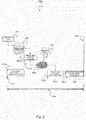
- Fig. 2 is a schematic diagram of a method 200 for error protection in a mobile receiver for protection against transmission errors.
- data may be processed.
- the resulting transport blocks or data transport blocks may be provided to protocol stack memory 203 for data storage.
- the physical layer processing block 207a may be started, e.g. Downlink receiver for Uplink grant.
- Physical layer processing 207a may provide grant 214 for higher layer and may request data for transmission.
- the higher layer protocol processing block 205a may retrieve a data transport block stored in memory buffer 203 and perform protocol processing on that data transport block.
- the processed data transport block may be stored in a first memory buffer 209, for example one memory buffer of the protocol stack memory 203. That first memory buffer 209 may be corrupted by memory errors 202 not detectable at receiver side.
- the physical layer processing block 207b may retrieve the processed data transport block corrupted by memory errors from the first memory buffer 209 and may perform transmit error protection on that block, e.g. by attaching CRC, to allow detecting blocks which have been corrupted on the air and cannot be decoded any more 204.
- the physical layer processing block 207c may further perform FEC (forward error correction) encoding and modulation on that block to allow correcting blocks which have been corrupted on the air 206.
- FEC forward error correction
- time constraint 208 there is a tight time constraint 208 from start of processing a data transport block triggered by uplink grant arrival over the air 212 until deadline 210 for data transmission over the air.
- Such a time constraint 208 may be in a range of about 4 milliseconds and smaller in an exemplary LTE transmission. Processing has to be completed within such time frame 208.
- Some sorts of data, e.g. higher layer control or user data before doing the channel encoding for an uplink transmission are particularly sensitive as errors cannot be detected on the receiving side (e.g. an LTE base station/eNodeB) . Due to the short latency requirement and fast responsiveness of e.g. LTE a simple detection and re-transmission from higher protocol layers may be not practical. Therefore, a full-blown ECC protection may be required as illustrated in Figures 3 and 4 . These figures give an overview of the implications of memory errors in the uplink transmission chain.
- Fig. 3 is a schematic diagram of a method 300 for memory error detection in a mobile receiver using higher layer protocol processing.
- data may be processed as described above with respect to Fig. 2 .
- the resulting transport blocks or data transport blocks may be provided to protocol stack memory 203 for data storage.
- the physical layer processing block 207a may be started, e.g. Downlink receiver for Uplink grant.
- Physical layer processing 207a may provide grant 214 for higher layer and may request data for transmission.
- the higher layer protocol processing block 205a may retrieve a data transport block stored in memory 203 and perform protocol processing on that data transport block.
- the processed data transport block may be stored in a first memory buffer 209 as described above with respect to Fig. 2 .
- That first memory buffer 209 may be corrupted by memory errors 202 not detectable at receiver side.
- An error detection block 301 may detect one or more errors in a data transport block retrieved from the first memory buffer 209 and may indicate a resend request 302 to the higher layer protocol processing block 205b.
- the higher layer processing block 305b may retrieve the data transport block from the memory 203 one more time and store the retrieved data transport block in a second memory buffer 309 for further processing.
- the physical layer processing block 207b may retrieve the data transport block from the second memory buffer 309 for physical layer processing, e.g. CRC attachment etc.
- the deadline 210 for data transmission over the air may be exceeded that may result in a violation 304 of timing constraints.
- Fig. 4 is a schematic diagram of a method 400 for error protection in a mobile receiver using error correction and ECC overhead.
- data may be processed as described above with respect to Figs. 2 and 3 .
- the resulting transport blocks or data transport blocks may be provided to protocol stack memory 203 for data storage.
- the physical layer processing block 207a may be started, e.g. Downlink receiver for Uplink grant.
- Physical layer processing 207a may provide grant 214 for higher layer and may request data for transmission.
- the higher layer protocol processing block 205a may retrieve a data transport block stored in memory 203 and perform protocol processing on that data transport block.
- the processed data transport block may be stored in a first memory buffer 209 as described above with respect to Figs. 2 and 3 .
- the processed data transport block may be stored in an ECC overhead or redundant buffer 409 protecting the first memory buffer 209.
- error correction may be performed during reading by an error correction block 401.
- the error correction block 401 may detect an error in the data transport block retrieved from the first memory buffer 209 and may correct the data transport block based on information of both memory buffers, the first memory buffer 209 and the redundant memory buffer 409.
- the erroneous data transport block of the first memory buffer 209 is replaced by the correct data transport block of the redundant memory buffer 409.
- redundancy bits stored in the redundant memory buffer 409 may be used to correct the data transport block of the first memory buffer 209.
- the physical layer processing block 207b may receive the corrected data transport block and may perform physical layer processing, e.g. CRC attachment etc.
- a further physical layer processing block 207c may perform physical layer processing with respect to FEC encoding, modulation etc. as described above with respect to Fig. 2 . Due to the redundant memory buffer 409 and error correction during read 401 the deadline 210 for data transmission over the air may be met.
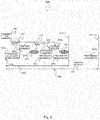
- Fig. 5 is a schematic diagram of a method 500 for error protection in a mobile receiver using a processing chain in accordance with the disclosure.
- data may be processed as described above with respect to Figs. 2 to 4 .
- the resulting transport blocks or data transport blocks may be provided to protocol stack memory 203 for data storage.
- the physical layer processing block 207a may be started, e.g. Downlink receiver for Uplink grant.
- Physical layer processing 207a may provide grant 214 for higher layer and may request data for transmission.
- the higher layer protocol processing block 205a may retrieve a data transport block stored in memory 203 and perform protocol processing on that data transport block.
- the processed data transport block may be stored in a first memory buffer 209 as described above with respect to Figs. 2 to 4 .
- That first memory buffer 209 may be corrupted by memory errors 202 not detectable at receiver side.
- An error detection block 501 may detect one or more errors in a data transport block retrieved from the first memory buffer 209.
- a CRC attachment block 503 an invalidated CRC may be attached to that erroneous data transport block and the erroneous data transport block with invalidated CRC may be passed to the physical layer processing block 207b for further processing such as FEC coding, modulation etc.
- a resend request 302 may be indicated to the higher layer protocol processing block 205b.
- the higher layer processing block 305b may retrieve the data transport block from the memory 203 one more time and store the retrieved data transport block in a second memory buffer 309 for further processing. Both tasks retrieving the data transport block once more and physical layer processing 207b may be finished within a processing time constraint 208.
- the erroneous data transport block may be detected 507 based on its invalidated CRC.
- the receiver may request re-transmission, e.g. according to a HARQ mechanism, and a retransmitted data transport block may be provided by the physical layer processing block 207b in the next time frame, i.e. until deadline 510 for data re-transmission over the air.
- the re-transmission may be completed within a more relaxed processing time constraint 508 that may be, for example twice the time constraint 208 for a single re-transmission plus round-trip time. Of course, more than one re-transmission may be performed.
- the method 500 may thus exploit the re-transmission capabilities as provided by the data communication standards such as HARQ combined with a low-complexity error detection to perform a real-time correction of memory errors.
- parity bits may be added to each data word written from the protocol stack 205a.
- the number of parity errors may be tracked for every data block which may be protected by appending cyclic redundancy check (CRC) bits, e.g. a code or transport block in LTE. If at least one parity error occurs in a block, the respective CRC bits may be invalidated by the block 503, e.g. preferably by flipping a single bit of the CRC bits or alternatively by flipping more than one bit of the CRC bits or by scrambling the CRC bits with a random bit sequence.
- CRC cyclic redundancy check
- the data block may be encoded and transmitted over the air by the block 207b while the error is reported back 302 to the protocol stack 205b.
- the receiving side e.g. an LTE base station will rate the data block as erroneous and request a re-transmission 507 from the sender. This is acceptable from a performance point of view as the memory error probability is significantly lower than the block error rate on the air.
- networks are dimensioned to work with block error rates of ⁇ 10%.
- the protocol stack is able to identify the corrupted data block and to resend it in time to the physical layer 207d before the re-transmission 508 has to be done.
- This solution significantly reduces the complexity of memory error correction by just adding a parity bit instead of a full-blown ECC.
- the method 500 prevents the receiving side from erroneously assuming the data block to be correct which would result in potentially severe user application or radio resource management errors.
- the standard re-transmission mechanisms and its round-trip delay sufficient time for reporting and correcting the data block is obtained, i.e. no severe time constraints are created by repairing the corrupt data block.
- the memory error rate is typically much smaller than the normal block error rate observed on the air.
- the method 500 can be used for all communication standards supporting some kind of re-transmission mechanisms, e.g. WLAN or wired standards such as DSL.
- Fig. 6 is a schematic diagram of a method 600 for error protection in a receiver in accordance with the disclosure.
- the method 600 protects a data transport block against memory errors and transmission errors.
- the method 600 includes attaching 601 a first redundancy section to the data transport block for protecting the data transport block against memory errors and providing the data transport block in a memory buffer, e.g. the first memory buffer 209 as described above with respect to Fig. 5 .
- the method 600 includes attaching 602 a second redundancy section to the data transport block read from the memory buffer for protecting the data transport block against transmission errors, e.g. a CRC as described above with respect to Fig. 5 , and providing the data transport block for transmission.
- the method 600 includes invalidating 603 the second redundancy section if an evaluation of the first redundancy section of the data transport block read from the memory buffer indicates a memory error, e.g. by attaching an invalidated CRC 503 as described above with respect to Fig. 5 .
- the method 600 may include providing the first redundancy section based on a parity check of the data transport block.
- the first redundancy section may include one or more parity bits indicating a parity of at least a part of the data transport block.
- the method 600 may include attaching a parity bit to the data transport block for each memory cell of the memory buffer in which the data transport block is provided, e.g. to each memory cell of the first memory buffer 209 as described above with respect to Fig. 5 .
- Such a memory cell may be a word of for example 4 bits, 8 bits, 16 bits or 32 bits. A higher word length results in a lower overhead but decreases the detectability.
- the evaluation of the first redundancy section may include counting a number of parity check errors while reading the data transport block from the memory buffer.
- the second redundancy section may be invalidated as soon as a first parity check error is detected or only if a specific number of parity check errors are detected.
- the method 600 may further include transmitting the data transport block attached with the invalidated second redundancy section if a memory error is indicated.
- the second redundancy section may be provided based on a cyclic redundancy check of the data transport block. Invalidating the second redundancy section may include reversing at least one bit of the second redundancy section or scrambling the second redundancy section with a scrambling sequence.
- the method 600 may include reporting an indicated memory error.
- the method 600 may include repairing the data transport block for which a memory error is reported; and providing the repaired data transport block for retransmission.
- the method 600 may include removing the first redundancy section from the data transport block when attaching the second redundancy section to the data transport block.
- the data transport block may be transmitted with CRC field, however, no parity bits as described above with respect to memory protection should be transmitted by the data transport block.
- the method 600 may include processing the data transport block and the attached second redundancy section for uplink transmission, e.g. by the physical layer processing block 207b as described above with respect to Fig. 5 .
- the method 600 may include processing the data transport block and the attached second redundancy section according to a HARQ transmission scheme.
- Fig. 7 is a block diagram of a device 700 for error protection against memory errors and transmission errors in a receiver in accordance with the disclosure.
- the device 700 includes a first protection circuit 701, a second protection circuit 703 and an invalidation circuit 705.
- the first protection circuit 701 is configured to attach a first redundancy section 704, e.g. one or more parity bits, to the data transport block 702 for protecting the data transport block 702 against memory errors and configured to provide the data transport block 702 with the first redundancy section 704 in a memory buffer, e.g. a first memory buffer 209 as described above with respect to Fig. 5 .
- the second protection circuit 703 is configured to attach a second redundancy section 706, e.g. a CRC checksum, to the data transport block 702 read from the memory buffer for protecting the data transport block 702 against transmission errors and configured to provide the data transport block 710 with the second redundancy section 706 for transmission.
- the invalidation circuit 705 is configured to invalidate the second redundancy section 706 if an evaluation of the first redundancy section 704 of the data transport block 702 read from the memory buffer indicates a memory error. Then the data transport block 708 with the invalidated second redundancy section 706 may be provided for transmission.
- the device 700 may include a parity check circuit to check a parity of the data transport block 702.
- the first protection circuit 701 may be configured to provide the first redundancy section 704 based on the parity check of the data transport block 702.
- the device 700 may include a counter configured to count a number of parity check errors for the data transport block 702 read from the memory buffer.
- the device 700 may include a cyclic redundancy check processing circuit to process a cyclic redundancy check of the data transport block 702.
- the second protection circuit 703 may be configured to provide the second redundancy section 706 based on the cyclic redundancy check of the data transport block 702.
- the invalidation circuit 705 may include a bit reversing circuit configured to reverse at least one bit of the second redundancy section 706 to invalidate the second redundancy section 706.
- the invalidation circuit 705 may include a scrambler configured to scramble the second redundancy section 706 with a scrambling sequence, e.g. a random sequence, to invalidate the second redundancy section 706.
- the device 700 may further include a reporting circuit configured to report an indicated memory error.
- the device 700 may further include a protocol processing circuit, configured to repair the data transport block 702 for which a memory error is reported and to provide the repaired data transport block 702 for retransmission, e.g. a protocol processing circuit 207d as described above with respect to Fig. 5 .
- the device 700 may be implemented in any receiver, for example a wired networks receiver such as a DSL receiver or a mobile receiver such as an LTE receiver or WLAN receiver.
- a wired networks receiver such as a DSL receiver or a mobile receiver such as an LTE receiver or WLAN receiver.
- Fig. 8 is a block diagram of an on-chip system 800 for error protection in a receiver in accordance with the disclosure.
- the system 800 includes a first protection circuit 801, a second protection circuit 803 and an invalidation circuit 805.
- the first protection circuit 801 is configured to attach at least one parity bit 804 to the data transport block 802 for protecting the data transport block 802 against memory errors.
- the at least one parity bit 804 may be determined over at least a part of the data transport block 802 and may be configured to provide the data transport block 802 in a memory buffer, e.g. a first memory buffer 209 as described above with respect to Fig. 5 .
- the second protection circuit 803 is configured to attach a cyclic redundancy checksum 806 to the data transport block 802 read from the memory buffer for protecting the data transport block 802 against transmission errors and configured to provide the data transport block 802 for transmission.
- the invalidation circuit 805 is configured to invalidate the cyclic redundancy checksum 806 if an evaluation of the at least one parity bit 804 of the data transport block 802 read from the memory buffer indicates a parity error.
- the system 800 may include a protocol processing circuit, e.g. a block 207d as described above with respect to Fig. 5 , configured to repair the data transport block 802 for which a parity error is indicated and to provide the repaired data transport block for retransmission.
- the invalidation circuit 805 may correspond to the invalidation circuit 705 as described above with respect to Fig. 7 .
- the on-chip system 800 may be implemented in any receiver, for example a wired networks receiver such as a DSL receiver or a mobile receiver such as an LTE receiver or WLAN receiver.
- a wired networks receiver such as a DSL receiver or a mobile receiver such as an LTE receiver or WLAN receiver.
- Fig. 9 is a block diagram of an on-chip system 900 for error protection in a mobile receiver in accordance with the disclosure.
- the on-chip system 900 includes a protocol stack 902 and a physical layer 904 which are coupled by a data buffer 209, e.g. a first memory buffer 209 as described above with respect to Fig. 5 .
- a user application block e.g. for Voice over LTE
- a radio resource control block 903 to a logical and transport channel processing block 905 for providing a data transport block attached with one or more parity bits to the data buffer 909 in which one or more memory errors 202 may occur as described above with respect to Figures 5 to 8 .
- a CRC attachment 907 may be implemented for attaching a CRC checksum to a data transport block retrieved from the data buffer 909.
- the CRC attachment block 907 may attach an invalidated CRC to the data transport block if the data transport block retrieved from the data buffer 909 is corrupted by a memory error 202 which corruption may be detected according to the mechanisms described above with respect to Figures 5 to 8 .
- the data transport block may be passed to channel encoding 921 and physical channel processing 911 for uplink transmission 915.
- a pre-notice time e.g. constrained by standard
- a pre-notice time may be received within an uplink scheduling information block 913 for providing timing constraints, e.g. timing constraints 208 and/or timing constraints including round-trip delay 508 as described above with respect to Fig. 5 to the logical and transport channel processing block 905.
- timing constraints e.g. timing constraints 208 and/or timing constraints including round-trip delay 508 as described above with respect to Fig. 5 to the logical and transport channel processing block 905.
- a re-transmission may be scheduled by the protocol stack 902.
- the protocol stack 902 may implement the blocks 205a, 205b as described above with respect to Fig. 5 .
- the physical layer 904 may implement the blocks 207a, 207b, 207c, 207d, 501, 503 as described above with respect to Fig. 5 .
- the blocks described in Fig. 9 may have the same functionalities as corresponding blocks described above with respect to Figures 7 and 8 .
- Methods and devices according to the disclosure may be based on the assumption that higher protocol stack layers provide the data for uplink transmission (e.g. an LTE transport block) in an on-chip memory buffer to the physical layer. Usually, this buffer is preserved inside the physical layer for potential re-transmissions. As the buffer may not be duplicated somewhere else, the complete higher layer processing may be required to "repair" a corrupt data block.
- the hardware While writing to the buffer, the hardware may add a parity bit per data word. As the bit error rate is considered to be low (or example in the range of 10 -6 ) a simple parity bit may already allow detecting most bit errors. The number of parity check errors can be counted while reading from the buffer.
- the parity check error counter may be reset for every data block which may be protected by its own CRC ("CRC block"), e.g. a HSUPA transport block or an LTE code or transport block. If any parity check error occurs inside a CRC block, it may be marked as erroneous and immediately reported back to the higher layers of the protocol stack. As soon as the higher layers are notified, they can start to prepare the re-transmission to the physical layer. Meanwhile the physical layer may continue preparing the uplink transmission, i.e. it may read the complete data block from memory and may compute a CRC.
- CRC block CRC block
- the physical layer may invalidate the CRC, e.g. by scrambling it with a random bit sequence. With this mechanism, the CRC block can be identified as being erroneous on the receiving side.
- the physical layer may afterwards continue its uplink processing and may transmit the data block over the air.
- the receiving side e.g. a base station
- the receiving side may demodulate and decode the data block and after the "provoked" CRC failure may initiate a normal re-transmission.
- a major advantage of most uplink re-transmission schemes is the synchronous HARQ scheme, i.e. an uplink re-transmission only happens at a pre-determined point in time. This can be exploited to further relax the timing constraint by pulling in the uplink processing as soon as a failure is detected.
- the present disclosure also supports a computer program product including computer executable code or computer executable instructions that, when executed, causes at least one computer to execute the performing and computing steps described herein, in particular the methods 500 and 600 as described above with respect to Figs. 5 and 6 and the techniques described above with respect to Figs. 1 to 9 .
- a computer program product may include a readable storage medium storing program code thereon for use by a computer.
- the program code may perform the method 500 as described above with respect to Fig. 5 or the method 600 as described above with respect to Fig. 6 .
Landscapes
- Engineering & Computer Science (AREA)
- Computer Networks & Wireless Communication (AREA)
- Signal Processing (AREA)
- Theoretical Computer Science (AREA)
- General Engineering & Computer Science (AREA)
- Quality & Reliability (AREA)
- Physics & Mathematics (AREA)
- General Physics & Mathematics (AREA)
- Computer Security & Cryptography (AREA)
- Detection And Prevention Of Errors In Transmission (AREA)
- Error Detection And Correction (AREA)
Claims (11)
- Verfahren (600) zum Schützen eines Datentransportblocks (702) vor Speicherfehlern und Übertragungsfehlern, wobei das Verfahren Folgendes umfasst:Bereitstellen eines ersten Redundanzabschnitts (704) basierend auf einer Paritätsprüfung des Datentransportblocks (702);Anfügen (601) des ersten Redundanzabschnitts (704) an den Datentransportblock (702) zum Schützen des Datentransportblocks (702) vor Speicherfehlern, und Bereitstellen des Datentransportblocks (702) in einem Speicherpuffer;Anfügen (602) eines zweiten Redundanzabschnitts (706) an den aus dem Speicherpuffer ausgelesenen Datentransportblock (702) zum Schützen des Datentransportblocks (702) vor Übertragungsfehlern, und Bereitstellen des Datentransportblocks (702) für Übertragung;Invalidieren (603) des zweiten Redundanzabschnitts (706), falls eine Bewertung des ersten Redundanzabschnitts (704) des aus dem Speicherpuffer ausgelesenen Datentransportblocks (702) einen Speicherfehler anzeigt;Übertragen des mit dem invalidierten zweiten Redundanzabschnitt (706) verbundenen (602) Datentransportblocks (702), falls ein Speicherfehler anzeigt wird;Melden des angezeigten Speicherfehlers;Reparieren des Datentransportblocks, für den der angezeigte Speicherfehler gemeldet wird; undBereitstellen des reparierten Datentransportblocks für Neuübertragung.
- Verfahren (600) nach Anspruch 1,
wobei der erste Redundanzabschnitt (704) mindestens ein Paritätsbit umfasst, das eine Parität von mindestens einem Teil des Datentransportblocks (702) angibt. - Verfahren (600) nach Anspruch 1 oder 2, das ferner Folgendes umfasst:
Anfügen eines Paritätsbits an den Datentransportblock (702) für jede Speicherzelle des Speicherpuffers, in dem der Datentransportblock (702) vorhanden ist. - Verfahren (600) nach einem der vorhergehenden Ansprüche,
wobei die Bewertung des ersten Redundanzabschnitts (704) das Zählen einer Anzahl von Paritätsprüfungsfehlern umfasst, während der Datentransportblock (702) aus dem Speicherpuffer ausgelesen wird. - Verfahren (600) nach einem der vorhergehenden Ansprüche, das ferner Folgendes umfasst:
Invalidieren des zweiten Redundanzabschnitts (706), sobald ein erster Paritätsprüfungsfehler erkannt wird. - Verfahren (600) nach einem der vorhergehenden Ansprüche, das ferner Folgendes umfasst:
Bereitstellen des zweiten Redundanzabschnitts (706) basierend auf einer zyklischen Redundanzprüfung des Datentransportblocks (702). - Verfahren (600) nach einem der vorhergehenden Ansprüche,
wobei das Invalidieren des zweiten Redundanzabschnitts (706) das Umkehren von mindestens einem Bit des zweiten Redundanzabschnitts (706) oder das Scrambeln des zweiten Redundanzabschnitts (706) mit einer Scrambling-Sequenz umfasst. - Vorrichtung (700) zum Schützen eines Datentransportblocks (702) vor Speicherfehlern und Übertragungsfehlern, wobei die Vorrichtung Folgendes umfasst:eine Paritätsprüfungsschaltung, die dazu ausgelegt ist, eine Parität des Datentransportblocks (702) zu prüfen;eine erste Schutzschaltung (701), die dazu ausgelegt ist, einen ersten Redundanzabschnitt (704) an den Datentransportblock (702) anzufügen, um den Datentransportblock vor Speicherfehlern zu schützen, und die dazu ausgelegt ist, den Datentransportblock in einem Speicherpuffer bereitzustellen,wobei die erste Schutzschaltung (701) dazu ausgelegt ist, den ersten Redundanzabschnitt (704) auf der Basis der Paritätsprüfung des Datentransportblocks (702) bereitzustellen;eine zweite Schutzschaltung (703), die dazu ausgelegt ist, einen zweiten Redundanzabschnitt (706) an den aus dem Speicherpuffer ausgelesenen Datentransportblock anzufügen, um den Datentransportblock (702) vor Übertragungsfehlern zu schützen, und die dazu ausgelegt ist, den Datentransportblock für Übertragung bereitzustellen;eine Invalidierungsschaltung (705), die dazu ausgelegt ist, den zweiten Redundanzabschnitt (706) zu invalidieren, falls eine Bewertung des ersten Redundanzabschnitts (704) des aus dem Speicherpuffer ausgelesenen Datentransportblocks einen Speicherfehler angibt, und den mit dem invalidierten zweiten Redundanzabschnitt (706) verbundenen Datentransportblock (702) zu übertragen, falls ein Speicherfehler angezeigt wird;eine Meldeschaltung, die dazu ausgelegt ist, den angezeigten Speicherfehler zu melden; undeine Protokollverarbeitungsschaltung, die dazu ausgelegt ist, den Datentransportblock, für den der angezeigte Speicherfehler gemeldet wird, zu reparieren, und den reparierten Datentransportblock für Neuübertragung bereitzustellen.
- Vorrichtung (700) nach Anspruch 8, die ferner Folgendes umfasst:
einen Zähler, der dazu ausgelegt ist, eine Anzahl von Paritätsprüfungsfehlern für den aus dem Speicherpuffer ausgelesenen Datentransportblock (702) zu zählen. - Vorrichtung (700) gemäß Anspruch 8 oder 9, wobei die Invalidierungsschaltung (705) Folgendes umfasst:
eine Bitumkehrschaltung, die dazu ausgelegt ist, mindestens ein Bit des zweiten Redundanzabschnitts (706) umzukehren, um den zweiten Redundanzabschnitt (706) zu invalidieren. - Vorrichtung (700) gemäß Anspruch 8 oder 9, wobei die Invalidierungsschaltung (705) Folgendes umfasst:
einen Scrambler, der dazu ausgelegt ist, den zweiten Redundanzabschnitt (706) mit einer Scrambling-Sequenz zu scrambeln, um den zweiten Redundanzabschnitt (706) zu invalidieren.
Applications Claiming Priority (1)
| Application Number | Priority Date | Filing Date | Title |
|---|---|---|---|
| DE102015103809.9A DE102015103809B3 (de) | 2015-03-16 | 2015-03-16 | Verfahren und Vorrichtung zum Schützen eines Datentransportblocks gegen Speicherfehler und Übertragungsfehler |
Publications (2)
| Publication Number | Publication Date |
|---|---|
| EP3070865A1 EP3070865A1 (de) | 2016-09-21 |
| EP3070865B1 true EP3070865B1 (de) | 2019-11-27 |
Family
ID=55456564
Family Applications (1)
| Application Number | Title | Priority Date | Filing Date |
|---|---|---|---|
| EP16153642.0A Active EP3070865B1 (de) | 2015-03-16 | 2016-02-01 | Verfahren und vorrichtung zum schutz eines datentransportblocks gegen speicherfehler und übertragungsfehler |
Country Status (5)
| Country | Link |
|---|---|
| US (1) | US10063346B2 (de) |
| EP (1) | EP3070865B1 (de) |
| CN (1) | CN105991252B (de) |
| DE (1) | DE102015103809B3 (de) |
| TW (1) | TWI608491B (de) |
Families Citing this family (9)
| Publication number | Priority date | Publication date | Assignee | Title |
|---|---|---|---|---|
| KR20180106495A (ko) * | 2017-03-20 | 2018-10-01 | 에스케이하이닉스 주식회사 | 반도체장치 |
| CN108958961B (zh) * | 2017-05-22 | 2021-11-30 | 上海宝存信息科技有限公司 | 数据储存装置以及数据错误管理方法 |
| US10635554B2 (en) | 2017-07-19 | 2020-04-28 | Dell Products, L.P. | System and method for BIOS to ensure UCNA errors are available for correlation |
| US10656615B2 (en) * | 2018-01-18 | 2020-05-19 | Mitsubishi Electric Corporation | PLC, network unit, CPU, and data transfer method |
| CN110166166B (zh) * | 2018-02-14 | 2022-01-28 | 瑞昱半导体股份有限公司 | 网络数据处理装置及方法 |
| US11086713B1 (en) * | 2019-07-23 | 2021-08-10 | Pure Storage, Inc. | Optimized end-to-end integrity storage system |
| WO2021030947A1 (en) * | 2019-08-16 | 2021-02-25 | Qualcomm Incorporated | Bundling and timeline determination for multiple transport blocks scheduled by a single downlink control information message |
| KR20210157863A (ko) * | 2020-06-22 | 2021-12-29 | 에스케이하이닉스 주식회사 | 메모리, 메모리 시스템 및 메모리의 동작 방법 |
| TWI826133B (zh) | 2022-11-21 | 2023-12-11 | 瑞昱半導體股份有限公司 | 資料傳輸裝置與跨時脈領域資料傳輸之方法 |
Family Cites Families (15)
| Publication number | Priority date | Publication date | Assignee | Title |
|---|---|---|---|---|
| KR100659265B1 (ko) | 2000-11-10 | 2006-12-20 | 삼성전자주식회사 | 패리티비트가 역순으로 부가된 씨.알.씨. 코드의에러검출장치 및 방법 |
| US7047475B2 (en) | 2003-02-04 | 2006-05-16 | Hewlett-Packard Development Company, L.P. | CRC encoding scheme for conveying status information |
| KR20050027679A (ko) * | 2003-09-16 | 2005-03-21 | 삼성전자주식회사 | 이동통신시스템에서 고속 패킷 데이터 송/수신장치 및 방법 |
| WO2008096304A2 (en) * | 2007-02-09 | 2008-08-14 | Nxp B.V. | Transmission method, transmitter and data processing system comprising a transmitter |
| US20080205568A1 (en) * | 2007-02-28 | 2008-08-28 | Matsushita Electric Industrial Co., Ltd. | Dsrc communication circuit and dsrc communication method |
| US8379738B2 (en) * | 2007-03-16 | 2013-02-19 | Samsung Electronics Co., Ltd. | Methods and apparatus to improve performance and enable fast decoding of transmissions with multiple code blocks |
| US7853857B2 (en) * | 2007-09-14 | 2010-12-14 | Motorola Mobility, Inc. | Multi-layer cyclic redundancy check code in wireless communication system |
| US8737517B2 (en) | 2008-03-26 | 2014-05-27 | Qualcomm Incorporated | Scrambling and modulation to constrain the constellation size of ACK/NAK transmission on the data channel |
| WO2011111234A1 (ja) * | 2010-03-12 | 2011-09-15 | 富士通株式会社 | 受信機、受信方法及び無線通信システム |
| US8874808B2 (en) * | 2010-09-07 | 2014-10-28 | International Business Machines Corporation | Hierarchical buffer system enabling precise data delivery through an asynchronous boundary |
| US8635390B2 (en) * | 2010-09-07 | 2014-01-21 | International Business Machines Corporation | System and method for a hierarchical buffer system for a shared data bus |
| US8553469B2 (en) * | 2011-04-06 | 2013-10-08 | Dell Products L.P. | Memory buffer for buffer-on-board applications |
| CN102263612B (zh) * | 2011-07-18 | 2014-12-17 | 杭州承联通信技术有限公司 | 用于数据块的差错检测方法和设备 |
| JP5597224B2 (ja) | 2012-05-11 | 2014-10-01 | 株式会社東芝 | 情報記憶装置およびメモリ異常処理方法 |
| US9543981B2 (en) * | 2014-03-25 | 2017-01-10 | Texas Instruments Incorporated | CRC-based forward error correction circuitry and method |
-
2015
- 2015-03-16 DE DE102015103809.9A patent/DE102015103809B3/de not_active Expired - Fee Related
-
2016
- 2016-01-12 US US14/993,311 patent/US10063346B2/en not_active Expired - Fee Related
- 2016-02-01 EP EP16153642.0A patent/EP3070865B1/de active Active
- 2016-02-03 TW TW105103608A patent/TWI608491B/zh not_active IP Right Cessation
- 2016-02-16 CN CN201610086718.6A patent/CN105991252B/zh not_active Expired - Fee Related
Non-Patent Citations (1)
| Title |
|---|
| None * |
Also Published As
| Publication number | Publication date |
|---|---|
| EP3070865A1 (de) | 2016-09-21 |
| CN105991252A (zh) | 2016-10-05 |
| US10063346B2 (en) | 2018-08-28 |
| US20160277148A1 (en) | 2016-09-22 |
| TW201642275A (zh) | 2016-12-01 |
| CN105991252B (zh) | 2020-03-20 |
| TWI608491B (zh) | 2017-12-11 |
| DE102015103809B3 (de) | 2016-07-07 |
Similar Documents
| Publication | Publication Date | Title |
|---|---|---|
| US10063346B2 (en) | Method and device for protecting a data transport block against memory errors and transmission errors | |
| US20200112394A1 (en) | Code block level error correction and media access control (mac) level hybrid automatic repeat requests to mitigate bursty puncturing and interference in a multi-layer protocol wireless system | |
| JP6736554B2 (ja) | バースト性干渉の軽減 | |
| EP2924907B1 (de) | Konzept zur kombination codierter datenpakete mit robustem headerschutz | |
| WO2017156773A1 (en) | Hybrid automatic repeat request (harq) with polar coded transmissions | |
| US10721020B2 (en) | Parity frame | |
| US10338996B2 (en) | Pipelined decoder and method for conditional storage | |
| US20130346826A1 (en) | Low complexity error correction using cyclic redundancy check (CRC) | |
| US6728920B1 (en) | Method for correcting errors in transfer of information | |
| EP1357691B1 (de) | Verfahren zur Kodierung eines Benutzeridentifikator in einem Kommunikationssystem | |
| US9001936B2 (en) | Buffer management device and method for hybrid automatic repeat requests in a wireless communication system | |
| US20220217710A1 (en) | Method and Device for Detecting Partial Discontinuous Transmission (DTX) Using Soft Bits Correlation | |
| CN104838612B (zh) | 用于接收器中断事件后的改进的harq进程的方法和设备 | |
| US8793562B2 (en) | Apparatus and method for decoding in mobile communication system | |
| US12160923B2 (en) | Method and device for detecting partial discontinuous transmission (DTX) using bits reconstruction | |
| Garg et al. | An introduction to various error detection and correction schemes used in communication | |
| Singh et al. | Data Link Layer Designing Issues: Error Control-A Roadmap | |
| EP2061176B1 (de) | Inkrementelle Redundanz mit Resegmentierung | |
| EP3602881A1 (de) | Bestätigungssignalisierung in der kommunikation | |
| JPH09130368A (ja) | データ通信装置 | |
| HK40069793B (en) | A method and device for detecting partial discontinuous transmission (dtx) using soft bits correlation | |
| Soltani et al. | Performance evaluation of error control protocols over finite-state Markovian channels | |
| Bakhtiyari | Performance evaluation of adaptive hybrid ARQ systems | |
| KR20080049317A (ko) | 무선통신 시스템에서 송신 패킷 오류 검출 장치 및 방법 |
Legal Events
| Date | Code | Title | Description |
|---|---|---|---|
| PUAI | Public reference made under article 153(3) epc to a published international application that has entered the european phase |
Free format text: ORIGINAL CODE: 0009012 |
|
| 17P | Request for examination filed |
Effective date: 20160201 |
|
| AK | Designated contracting states |
Kind code of ref document: A1 Designated state(s): AL AT BE BG CH CY CZ DE DK EE ES FI FR GB GR HR HU IE IS IT LI LT LU LV MC MK MT NL NO PL PT RO RS SE SI SK SM TR |
|
| AX | Request for extension of the european patent |
Extension state: BA ME |
|
| STAA | Information on the status of an ep patent application or granted ep patent |
Free format text: STATUS: EXAMINATION IS IN PROGRESS |
|
| 17Q | First examination report despatched |
Effective date: 20181102 |
|
| GRAP | Despatch of communication of intention to grant a patent |
Free format text: ORIGINAL CODE: EPIDOSNIGR1 |
|
| STAA | Information on the status of an ep patent application or granted ep patent |
Free format text: STATUS: GRANT OF PATENT IS INTENDED |
|
| INTG | Intention to grant announced |
Effective date: 20190621 |
|
| GRAS | Grant fee paid |
Free format text: ORIGINAL CODE: EPIDOSNIGR3 |
|
| GRAA | (expected) grant |
Free format text: ORIGINAL CODE: 0009210 |
|
| STAA | Information on the status of an ep patent application or granted ep patent |
Free format text: STATUS: THE PATENT HAS BEEN GRANTED |
|
| AK | Designated contracting states |
Kind code of ref document: B1 Designated state(s): AL AT BE BG CH CY CZ DE DK EE ES FI FR GB GR HR HU IE IS IT LI LT LU LV MC MK MT NL NO PL PT RO RS SE SI SK SM TR |
|
| REG | Reference to a national code |
Ref country code: GB Ref legal event code: FG4D |
|
| REG | Reference to a national code |
Ref country code: CH Ref legal event code: EP |
|
| REG | Reference to a national code |
Ref country code: AT Ref legal event code: REF Ref document number: 1207920 Country of ref document: AT Kind code of ref document: T Effective date: 20191215 |
|
| REG | Reference to a national code |
Ref country code: DE Ref legal event code: R096 Ref document number: 602016024914 Country of ref document: DE |
|
| REG | Reference to a national code |
Ref country code: IE Ref legal event code: FG4D |
|
| REG | Reference to a national code |
Ref country code: NL Ref legal event code: FP |
|
| REG | Reference to a national code |
Ref country code: LT Ref legal event code: MG4D |
|
| PG25 | Lapsed in a contracting state [announced via postgrant information from national office to epo] |
Ref country code: GR Free format text: LAPSE BECAUSE OF FAILURE TO SUBMIT A TRANSLATION OF THE DESCRIPTION OR TO PAY THE FEE WITHIN THE PRESCRIBED TIME-LIMIT Effective date: 20200228 Ref country code: LT Free format text: LAPSE BECAUSE OF FAILURE TO SUBMIT A TRANSLATION OF THE DESCRIPTION OR TO PAY THE FEE WITHIN THE PRESCRIBED TIME-LIMIT Effective date: 20191127 Ref country code: BG Free format text: LAPSE BECAUSE OF FAILURE TO SUBMIT A TRANSLATION OF THE DESCRIPTION OR TO PAY THE FEE WITHIN THE PRESCRIBED TIME-LIMIT Effective date: 20200227 Ref country code: NO Free format text: LAPSE BECAUSE OF FAILURE TO SUBMIT A TRANSLATION OF THE DESCRIPTION OR TO PAY THE FEE WITHIN THE PRESCRIBED TIME-LIMIT Effective date: 20200227 Ref country code: SE Free format text: LAPSE BECAUSE OF FAILURE TO SUBMIT A TRANSLATION OF THE DESCRIPTION OR TO PAY THE FEE WITHIN THE PRESCRIBED TIME-LIMIT Effective date: 20191127 Ref country code: LV Free format text: LAPSE BECAUSE OF FAILURE TO SUBMIT A TRANSLATION OF THE DESCRIPTION OR TO PAY THE FEE WITHIN THE PRESCRIBED TIME-LIMIT Effective date: 20191127 Ref country code: FI Free format text: LAPSE BECAUSE OF FAILURE TO SUBMIT A TRANSLATION OF THE DESCRIPTION OR TO PAY THE FEE WITHIN THE PRESCRIBED TIME-LIMIT Effective date: 20191127 |
|
| PG25 | Lapsed in a contracting state [announced via postgrant information from national office to epo] |
Ref country code: RS Free format text: LAPSE BECAUSE OF FAILURE TO SUBMIT A TRANSLATION OF THE DESCRIPTION OR TO PAY THE FEE WITHIN THE PRESCRIBED TIME-LIMIT Effective date: 20191127 Ref country code: HR Free format text: LAPSE BECAUSE OF FAILURE TO SUBMIT A TRANSLATION OF THE DESCRIPTION OR TO PAY THE FEE WITHIN THE PRESCRIBED TIME-LIMIT Effective date: 20191127 Ref country code: IS Free format text: LAPSE BECAUSE OF FAILURE TO SUBMIT A TRANSLATION OF THE DESCRIPTION OR TO PAY THE FEE WITHIN THE PRESCRIBED TIME-LIMIT Effective date: 20200327 |
|
| REG | Reference to a national code |
Ref country code: DE Ref legal event code: R082 Ref document number: 602016024914 Country of ref document: DE Representative=s name: BARDEHLE PAGENBERG PARTNERSCHAFT MBB PATENTANW, DE Ref country code: DE Ref legal event code: R081 Ref document number: 602016024914 Country of ref document: DE Owner name: APPLE INC., CUPERTINO, US Free format text: FORMER OWNER: INTEL IP CORPORATION, SANTA CLARA, CALIF., US Ref country code: DE Ref legal event code: R081 Ref document number: 602016024914 Country of ref document: DE Owner name: APPLE INC., CUPERTINO, US Free format text: FORMER OWNER: INTEL IP CORPORATION, SANTA CLARA, CA, US |
|
| PG25 | Lapsed in a contracting state [announced via postgrant information from national office to epo] |
Ref country code: AL Free format text: LAPSE BECAUSE OF FAILURE TO SUBMIT A TRANSLATION OF THE DESCRIPTION OR TO PAY THE FEE WITHIN THE PRESCRIBED TIME-LIMIT Effective date: 20191127 |
|
| PG25 | Lapsed in a contracting state [announced via postgrant information from national office to epo] |
Ref country code: DK Free format text: LAPSE BECAUSE OF FAILURE TO SUBMIT A TRANSLATION OF THE DESCRIPTION OR TO PAY THE FEE WITHIN THE PRESCRIBED TIME-LIMIT Effective date: 20191127 Ref country code: EE Free format text: LAPSE BECAUSE OF FAILURE TO SUBMIT A TRANSLATION OF THE DESCRIPTION OR TO PAY THE FEE WITHIN THE PRESCRIBED TIME-LIMIT Effective date: 20191127 Ref country code: PT Free format text: LAPSE BECAUSE OF FAILURE TO SUBMIT A TRANSLATION OF THE DESCRIPTION OR TO PAY THE FEE WITHIN THE PRESCRIBED TIME-LIMIT Effective date: 20200419 Ref country code: CZ Free format text: LAPSE BECAUSE OF FAILURE TO SUBMIT A TRANSLATION OF THE DESCRIPTION OR TO PAY THE FEE WITHIN THE PRESCRIBED TIME-LIMIT Effective date: 20191127 Ref country code: RO Free format text: LAPSE BECAUSE OF FAILURE TO SUBMIT A TRANSLATION OF THE DESCRIPTION OR TO PAY THE FEE WITHIN THE PRESCRIBED TIME-LIMIT Effective date: 20191127 Ref country code: ES Free format text: LAPSE BECAUSE OF FAILURE TO SUBMIT A TRANSLATION OF THE DESCRIPTION OR TO PAY THE FEE WITHIN THE PRESCRIBED TIME-LIMIT Effective date: 20191127 |
|
| REG | Reference to a national code |
Ref country code: DE Ref legal event code: R097 Ref document number: 602016024914 Country of ref document: DE |
|
| PG25 | Lapsed in a contracting state [announced via postgrant information from national office to epo] |
Ref country code: SK Free format text: LAPSE BECAUSE OF FAILURE TO SUBMIT A TRANSLATION OF THE DESCRIPTION OR TO PAY THE FEE WITHIN THE PRESCRIBED TIME-LIMIT Effective date: 20191127 Ref country code: SM Free format text: LAPSE BECAUSE OF FAILURE TO SUBMIT A TRANSLATION OF THE DESCRIPTION OR TO PAY THE FEE WITHIN THE PRESCRIBED TIME-LIMIT Effective date: 20191127 |
|
| REG | Reference to a national code |
Ref country code: AT Ref legal event code: MK05 Ref document number: 1207920 Country of ref document: AT Kind code of ref document: T Effective date: 20191127 |
|
| REG | Reference to a national code |
Ref country code: CH Ref legal event code: PL |
|
| PLBE | No opposition filed within time limit |
Free format text: ORIGINAL CODE: 0009261 |
|
| STAA | Information on the status of an ep patent application or granted ep patent |
Free format text: STATUS: NO OPPOSITION FILED WITHIN TIME LIMIT |
|
| REG | Reference to a national code |
Ref country code: NL Ref legal event code: PD Owner name: APPLE INC.; US Free format text: DETAILS ASSIGNMENT: CHANGE OF OWNER(S), ASSIGNMENT; FORMER OWNER NAME: INTEL IP CORPORATION Effective date: 20200917 |
|
| REG | Reference to a national code |
Ref country code: BE Ref legal event code: MM Effective date: 20200229 |
|
| PG25 | Lapsed in a contracting state [announced via postgrant information from national office to epo] |
Ref country code: MC Free format text: LAPSE BECAUSE OF FAILURE TO SUBMIT A TRANSLATION OF THE DESCRIPTION OR TO PAY THE FEE WITHIN THE PRESCRIBED TIME-LIMIT Effective date: 20191127 Ref country code: LU Free format text: LAPSE BECAUSE OF NON-PAYMENT OF DUE FEES Effective date: 20200201 |
|
| 26N | No opposition filed |
Effective date: 20200828 |
|
| PG25 | Lapsed in a contracting state [announced via postgrant information from national office to epo] |
Ref country code: AT Free format text: LAPSE BECAUSE OF FAILURE TO SUBMIT A TRANSLATION OF THE DESCRIPTION OR TO PAY THE FEE WITHIN THE PRESCRIBED TIME-LIMIT Effective date: 20191127 Ref country code: PL Free format text: LAPSE BECAUSE OF FAILURE TO SUBMIT A TRANSLATION OF THE DESCRIPTION OR TO PAY THE FEE WITHIN THE PRESCRIBED TIME-LIMIT Effective date: 20191127 Ref country code: CH Free format text: LAPSE BECAUSE OF NON-PAYMENT OF DUE FEES Effective date: 20200229 Ref country code: LI Free format text: LAPSE BECAUSE OF NON-PAYMENT OF DUE FEES Effective date: 20200229 Ref country code: SI Free format text: LAPSE BECAUSE OF FAILURE TO SUBMIT A TRANSLATION OF THE DESCRIPTION OR TO PAY THE FEE WITHIN THE PRESCRIBED TIME-LIMIT Effective date: 20191127 |
|
| REG | Reference to a national code |
Ref country code: GB Ref legal event code: 732E Free format text: REGISTERED BETWEEN 20201105 AND 20201111 |
|
| PG25 | Lapsed in a contracting state [announced via postgrant information from national office to epo] |
Ref country code: IE Free format text: LAPSE BECAUSE OF NON-PAYMENT OF DUE FEES Effective date: 20200201 Ref country code: IT Free format text: LAPSE BECAUSE OF FAILURE TO SUBMIT A TRANSLATION OF THE DESCRIPTION OR TO PAY THE FEE WITHIN THE PRESCRIBED TIME-LIMIT Effective date: 20191127 |
|
| PGFP | Annual fee paid to national office [announced via postgrant information from national office to epo] |
Ref country code: FR Payment date: 20201210 Year of fee payment: 6 |
|
| PG25 | Lapsed in a contracting state [announced via postgrant information from national office to epo] |
Ref country code: BE Free format text: LAPSE BECAUSE OF NON-PAYMENT OF DUE FEES Effective date: 20200229 |
|
| PGFP | Annual fee paid to national office [announced via postgrant information from national office to epo] |
Ref country code: DE Payment date: 20210119 Year of fee payment: 6 Ref country code: GB Payment date: 20210120 Year of fee payment: 6 |
|
| PGFP | Annual fee paid to national office [announced via postgrant information from national office to epo] |
Ref country code: NL Payment date: 20211216 Year of fee payment: 7 |
|
| PG25 | Lapsed in a contracting state [announced via postgrant information from national office to epo] |
Ref country code: TR Free format text: LAPSE BECAUSE OF FAILURE TO SUBMIT A TRANSLATION OF THE DESCRIPTION OR TO PAY THE FEE WITHIN THE PRESCRIBED TIME-LIMIT Effective date: 20191127 Ref country code: MT Free format text: LAPSE BECAUSE OF FAILURE TO SUBMIT A TRANSLATION OF THE DESCRIPTION OR TO PAY THE FEE WITHIN THE PRESCRIBED TIME-LIMIT Effective date: 20191127 Ref country code: CY Free format text: LAPSE BECAUSE OF FAILURE TO SUBMIT A TRANSLATION OF THE DESCRIPTION OR TO PAY THE FEE WITHIN THE PRESCRIBED TIME-LIMIT Effective date: 20191127 |
|
| PG25 | Lapsed in a contracting state [announced via postgrant information from national office to epo] |
Ref country code: MK Free format text: LAPSE BECAUSE OF FAILURE TO SUBMIT A TRANSLATION OF THE DESCRIPTION OR TO PAY THE FEE WITHIN THE PRESCRIBED TIME-LIMIT Effective date: 20191127 |
|
| REG | Reference to a national code |
Ref country code: DE Ref legal event code: R119 Ref document number: 602016024914 Country of ref document: DE |
|
| GBPC | Gb: european patent ceased through non-payment of renewal fee |
Effective date: 20220201 |
|
| PG25 | Lapsed in a contracting state [announced via postgrant information from national office to epo] |
Ref country code: FR Free format text: LAPSE BECAUSE OF NON-PAYMENT OF DUE FEES Effective date: 20220228 |
|
| PG25 | Lapsed in a contracting state [announced via postgrant information from national office to epo] |
Ref country code: GB Free format text: LAPSE BECAUSE OF NON-PAYMENT OF DUE FEES Effective date: 20220201 Ref country code: DE Free format text: LAPSE BECAUSE OF NON-PAYMENT OF DUE FEES Effective date: 20220901 |
|
| REG | Reference to a national code |
Ref country code: NL Ref legal event code: MM Effective date: 20230301 |
|
| PG25 | Lapsed in a contracting state [announced via postgrant information from national office to epo] |
Ref country code: NL Free format text: LAPSE BECAUSE OF NON-PAYMENT OF DUE FEES Effective date: 20230301 |