EP3070842A1 - Verfahren und vorrichtung für die stromversorgung eines verstärkers - Google Patents
Verfahren und vorrichtung für die stromversorgung eines verstärkers Download PDFInfo
- Publication number
- EP3070842A1 EP3070842A1 EP15159312.6A EP15159312A EP3070842A1 EP 3070842 A1 EP3070842 A1 EP 3070842A1 EP 15159312 A EP15159312 A EP 15159312A EP 3070842 A1 EP3070842 A1 EP 3070842A1
- Authority
- EP
- European Patent Office
- Prior art keywords
- power amplifier
- output
- transmit signal
- output voltage
- power
- Prior art date
- Legal status (The legal status is an assumption and is not a legal conclusion. Google has not performed a legal analysis and makes no representation as to the accuracy of the status listed.)
- Withdrawn
Links
- 238000000034 method Methods 0.000 title claims abstract description 23
- 230000005540 biological transmission Effects 0.000 claims abstract description 77
- 238000004891 communication Methods 0.000 claims description 22
- 238000004590 computer program Methods 0.000 claims description 22
- 238000013461 design Methods 0.000 description 8
- 238000010586 diagram Methods 0.000 description 8
- 238000005516 engineering process Methods 0.000 description 5
- 239000004065 semiconductor Substances 0.000 description 5
- 238000006243 chemical reaction Methods 0.000 description 3
- 230000001413 cellular effect Effects 0.000 description 2
- 238000004519 manufacturing process Methods 0.000 description 2
- 230000007246 mechanism Effects 0.000 description 2
- 238000012986 modification Methods 0.000 description 2
- 230000004048 modification Effects 0.000 description 2
- 230000006978 adaptation Effects 0.000 description 1
- 230000002776 aggregation Effects 0.000 description 1
- 238000004220 aggregation Methods 0.000 description 1
- 238000003491 array Methods 0.000 description 1
- 238000013475 authorization Methods 0.000 description 1
- 230000010267 cellular communication Effects 0.000 description 1
- 230000008859 change Effects 0.000 description 1
- 230000008867 communication pathway Effects 0.000 description 1
- 239000004020 conductor Substances 0.000 description 1
- 238000013479 data entry Methods 0.000 description 1
- 230000001419 dependent effect Effects 0.000 description 1
- 239000000446 fuel Substances 0.000 description 1
- 238000003384 imaging method Methods 0.000 description 1
- 239000004973 liquid crystal related substance Substances 0.000 description 1
- 230000007774 longterm Effects 0.000 description 1
- 238000010295 mobile communication Methods 0.000 description 1
- 230000008569 process Effects 0.000 description 1
- 230000008054 signal transmission Effects 0.000 description 1
- 230000011664 signaling Effects 0.000 description 1
- 238000003860 storage Methods 0.000 description 1
- 239000000758 substrate Substances 0.000 description 1
Images


Classifications
-
- H—ELECTRICITY
- H03—ELECTRONIC CIRCUITRY
- H03F—AMPLIFIERS
- H03F3/00—Amplifiers with only discharge tubes or only semiconductor devices as amplifying elements
- H03F3/68—Combinations of amplifiers, e.g. multi-channel amplifiers for stereophonics
-
- H—ELECTRICITY
- H03—ELECTRONIC CIRCUITRY
- H03F—AMPLIFIERS
- H03F1/00—Details of amplifiers with only discharge tubes, only semiconductor devices or only unspecified devices as amplifying elements
- H03F1/02—Modifications of amplifiers to raise the efficiency, e.g. gliding Class A stages, use of an auxiliary oscillation
- H03F1/0205—Modifications of amplifiers to raise the efficiency, e.g. gliding Class A stages, use of an auxiliary oscillation in transistor amplifiers
- H03F1/0211—Modifications of amplifiers to raise the efficiency, e.g. gliding Class A stages, use of an auxiliary oscillation in transistor amplifiers with control of the supply voltage or current
- H03F1/0244—Stepped control
- H03F1/0255—Stepped control by using a signal derived from the output signal
-
- H—ELECTRICITY
- H03—ELECTRONIC CIRCUITRY
- H03F—AMPLIFIERS
- H03F1/00—Details of amplifiers with only discharge tubes, only semiconductor devices or only unspecified devices as amplifying elements
- H03F1/02—Modifications of amplifiers to raise the efficiency, e.g. gliding Class A stages, use of an auxiliary oscillation
- H03F1/0205—Modifications of amplifiers to raise the efficiency, e.g. gliding Class A stages, use of an auxiliary oscillation in transistor amplifiers
- H03F1/0277—Selecting one or more amplifiers from a plurality of amplifiers
-
- H—ELECTRICITY
- H03—ELECTRONIC CIRCUITRY
- H03F—AMPLIFIERS
- H03F3/00—Amplifiers with only discharge tubes or only semiconductor devices as amplifying elements
- H03F3/189—High-frequency amplifiers, e.g. radio frequency amplifiers
- H03F3/19—High-frequency amplifiers, e.g. radio frequency amplifiers with semiconductor devices only
- H03F3/195—High-frequency amplifiers, e.g. radio frequency amplifiers with semiconductor devices only in integrated circuits
-
- H—ELECTRICITY
- H03—ELECTRONIC CIRCUITRY
- H03F—AMPLIFIERS
- H03F3/00—Amplifiers with only discharge tubes or only semiconductor devices as amplifying elements
- H03F3/20—Power amplifiers, e.g. Class B amplifiers, Class C amplifiers
- H03F3/24—Power amplifiers, e.g. Class B amplifiers, Class C amplifiers of transmitter output stages
-
- H—ELECTRICITY
- H03—ELECTRONIC CIRCUITRY
- H03F—AMPLIFIERS
- H03F2200/00—Indexing scheme relating to amplifiers
- H03F2200/111—Indexing scheme relating to amplifiers the amplifier being a dual or triple band amplifier, e.g. 900 and 1800 MHz, e.g. switched or not switched, simultaneously or not
-
- H—ELECTRICITY
- H03—ELECTRONIC CIRCUITRY
- H03F—AMPLIFIERS
- H03F2200/00—Indexing scheme relating to amplifiers
- H03F2200/429—Two or more amplifiers or one amplifier with filters for different frequency bands are coupled in parallel at the input or output
-
- H—ELECTRICITY
- H03—ELECTRONIC CIRCUITRY
- H03F—AMPLIFIERS
- H03F2200/00—Indexing scheme relating to amplifiers
- H03F2200/511—Many discrete supply voltages or currents or voltage levels can be chosen by a control signal in an IC-block amplifier circuit
-
- H—ELECTRICITY
- H03—ELECTRONIC CIRCUITRY
- H03F—AMPLIFIERS
- H03F2200/00—Indexing scheme relating to amplifiers
- H03F2200/516—Some amplifier stages of an amplifier use supply voltages of different value
Definitions
- the present invention relates to a method for supplying power to an amplifier and an apparatus for supplying power to an amplifier.
- Some apparatuses which are able to transmit and receive signals wirelessly may be battery powered and supply power to a radio frequency (RF) power amplifier (PA) of a transmitter from the battery.
- RF radio frequency
- Such battery-operated wireless communication devices are, for example, mobile phones, personal digital assistants (PDA), etc.
- the power amplifier(s) may determine a large portion of the total power consumption of such devices.
- Batteries with low supply voltage, for example about 3 volts (V) or smaller than 3 V or higher than 3 V, for example 3.6 V or 3.7 V or 5 V, may be employed in the portable devices.
- Various embodiments provide a method and apparatus for supplying power to a power amplifier of a transmitter.
- a method comprising:
- an apparatus comprising:
- an apparatus comprising at least one processor and at least one memory including computer program code, the at least one memory and the computer program code configured to, with the at least one processor, cause the apparatus to:
- a computer program product including one or more sequences of one or more instructions which, when executed by one or more processors, cause an apparatus to at least perform the following:
- an apparatus comprising:
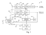
- Figure 1 depicts an example of a part of a device 100, which may be, for example, a mobile device such as a mobile phone, but may also be another device comprising the power amplifier 113.
- the device 100 may be constructed to include the frequency synthesizer 101 for generating one or more oscillator signals e.g. from a signal provided by a local oscillator 118.
- the device comprises one or more processors 102 for controlling the operation of the device, in accordance with an embodiment.
- the processor 102 operates in accordance with program instructions stored in at least one storage medium, such as at least one memory 103.
- the processor 102 may control the frequency synthesizer 101 for setting the output frequency/frequencies of the frequency synthesizer 101.
- the RF receiver circuitry 104 may include one or multiple instances of filters 105, amplifiers 106 and mixers 107.
- the one or multiple instances of mixers 107 may be adapted to receive signals from the one or multiple instances of amplifiers 106 and a first local oscillator signal LO1.
- the RF receiver circuitry 104 may be configured to be connected with at least one, and possibly several antennas 108, and may operate to simultaneously receive and downconvert multiple reception channels in multiple frequency bands.
- the RF receiver circuitry 104 may be implemented e.g.
- the downconverted signals from multiple reception channels are provided to at least one baseband circuitry block 109 to demodulate and decode received signaling and other data.
- the device of Figure 1 also comprises an RF transmitter 110 for transmitting radio frequency signals.
- the transmitter 110 may comprise one or more mixers 111 adapted to receive signals to be transmitted and a second local oscillator signal LO2.
- the mixing result may be provided to a power amplifier 113 to amplify the RF signals, and a band pass filter 112 to filter out mixing results which are out of the transmission band before passing them to one or more antennas 108.
- the mixing results which are passed through the band pass filter 112, in other words the wanted transmission signals, may be passed to the one or more antennas 108.
- the one or more antennas 108 may be the same one or more antennas than the RF receiver circuitry 104 uses or different antenna(s).
- the RF receiver circuitry 104, the RF transmitter 110 and/or the baseband circuitry 109 may be embodied as an integrated circuit.
- the RF receiver circuitry 104, the RF transmitter 110 and the baseband circuitry 109 may be embodied in the same integrated circuit, and in some other embodiments they may be embodied in different integrated circuits.
- all of the circuitry shown in Figure 1 including the processor 102 and possibly also the memory 103, may be embodied in one integrated circuit module or package.
- the functionality of the frequency synthesizer 101 may be embodied by the processor 102 or by another processor, such as a high speed digital signal processor operating under control of a stored program.
- the device 100 may comprise more than one RF receiver circuitry 104 and more than one RF transmitter 110 to enable simultaneous communication on multiple channels, multiple frequencies etc.
- the device 100 may further comprise more than one baseband circuitry 109.
- the device of Figure 1 also comprises an apparatus 200 for supplying power to the power amplifier 113 of the transmitter 110 of the device 100.
- Figure 2 depicts an example of the apparatus 200, in accordance with an embodiment.
- the apparatus 200 of Figure 2 comprises a multi-level power source 202, a multiplexer control element 204, a control element 206 for controlling the multi-level power source 202 and the multiplexer control element 204, and a set of multiplexers 208 for providing power to the RF power amplifiers 113.
- the output of the multiplexers 208 may be coupled to low-pass filters to filter out noise, peaks or other unwanted phenomena such as ripple from the voltage provided by the multiplexers 208.
- the output of the multiplexers 208 may be coupled to a controlled linear regulator.
- the device 100 may be communicating on one or more channels or modes wherein one or more modulating signals may be generated by the modem 115.
- the modulating signals 116 are provided to the multiplexer control element 204. In Figure 2 these signals are also referred with labels RF1, RF2, RF3. Although three signals are depicted, the number of signals may be different from three. For example, only one or two signals may occur at a time, or more than three signals may also occur in some situations.
- the modulating signals may be, for example, digital base band signals, or analog signals, wherein an analog to digital conversion may be needed to provide the multiplexer control element 204 with the modulating signals in a digital form.
- the modem 115 may also provide one or more transmission parameters 117 (tpar 1 ,...,tpar n ) to the control element 206 which the control element 206 may use to determine voltage levels needed by the power amplifiers 113. If the RF transmitter 110 is operating multiple power amplifiers 113 simultaneously, each power amplifier 113 may transmit its own transmission signal.
- the transmission signal has known transmission parameters, such as an average power level, modulation, resource block allocation etc.
- the control element 206 may analyze one or more of the transmission parameters of each transmission signal to determine voltage level or voltage levels needed by the power amplifiers 113 to be able to generate appropriate transmission signals.
- the control element 206 may use, for example, a lookup table (LUT) 207 in the voltage level determination, or another appropriate way to find out the voltage level to be supplied for each power amplifier 113.
- the lookup table 207 is illustrated in Figure 2 with a box within the control element 206 but in practical implementations the lookup table 207 may be constructed, for example, as a set of values in a memory addressable by input parameters.
- the lookup table may comprise as many dimensions as the number of transmission parameters which shall be used in the determination of the voltage level. Hence, the transmission parameters may be used as an index to the lookup table to find out the corresponding voltage level. It may, however, happen that the lookup table does not contain index values for the transmission parameters.
- the so called Delaunay triangulation may be used to linearly interpolate a multi-dimensional lookup table.
- control element 206 selects a voltage level for a power amplifier selected to transmit the transmission signal.
- the control element 206 may perform the voltage level determination for each active transmission signal using the signal's transmission parameters 117.
- control element 206 controls the multi-level power source 202 to generate corresponding voltages.
- the multi-level power source 202 comprises circuitry to generate multiple voltage outputs 210 having different voltage levels.
- the multi-level power source 202 may comprise four voltage outputs V 1 , V 2 , V 3 and V 4 , but may have less than four or more than four voltage outputs.
- the multi-level power source 202 also comprises a control input 212 for each voltage output, or the multi-level power source 202 may comprise a common control input for each voltage output.
- the multi-level power source 202 may comprise circuitry for forming output voltages which are higher than a battery voltage and/or circuitry which may be able to output voltages which are smaller than the battery voltage.
- the circuitry capable of providing voltages above the battery voltage may be called as boost converters and circuitry capable of providing voltages below the battery voltage may be called as buck converters.
- other types of voltage converter circuitry may be utilized by the multi-level power source 202 such as a voltage regulator which may convert an input voltage to a lower level output voltage.
- a first control output may provide a first control signal ctrl_V 1 to a first voltage control input of the multi-level power source 202
- a second control output may provide a second control signal ctrl_V 2 to a second voltage control input of the multi-level power source 202
- a third control output may provide a third control signal ctrl_V 3 to a third voltage control input of the multi-level power source 202
- a fourth control output may provide a fourth control signal ctrl_V 4 to a fourth voltage control input of the multi-level power source 202.
- the first control output ctrl_V 1 may provide a control signal to the multi-level power source 202 to output a first voltage value V 1 at the first output and the third control output ctrl_V 3 may provide a control signal to the multi-level power source 202 to output a third voltage value V 3 at the third output.
- the control outputs ctrl_V 1 , ctrl_V 2 , ctrl_V 3 , ctrl_V 4 may indicate the multi-level power source 202 which voltage levels need to be generated by the multi-level power source 202.
- the control outputs 214 of the control element 206 may also be connected to the multiplexer control element 204 to provide the multiplexer control element 204 information on the voltage outputs which the multi-level power source 202 is controlled to generate.
- the multiplexer control element 204 also examines the signal levels of each transmission signal RF 1 ,..,RF n and uses this information to determine the voltage levels to be supplied to the corresponding power amplifiers 113.
- the multiplexer control element 204 may provide the first multiplexer 208a a selection signal 218 (ctrl mux1 ) which induces the first multiplexer 208a to connect the first voltage output V 1 from the multi-level power source 202 to the output of the first multiplexer 208a.
- the first power amplifier 113a is supplied the first voltage V 1 .
- the multiplexer control element 204 may provide the first multiplexer 208a a selection signal which induces the first multiplexer 208a to connect the second voltage output V 2 from the multi-level power source 202 to the output of the first multiplexer 208a.
- the multiplexer control element 204 may control each multiplexer 208 so that the supply voltages 216 for each power amplifier 113 are sufficient for the power amplifiers to substantially accurately amplify the corresponding RF transmission signals.
- Figure 3 illustrates an example of a multiplexer output with reference to a transmission signal. It can be seen that the multiplexer output voltage follows the positive envelope of the RF transmission signal so that the multiplexer output voltage is the same or higher than the positive envelope of the RF transmission signal.
- one voltage outputs may be reserved only to a certain power amplifier, wherein that voltage output should not be used by the other power amplifiers.
- a reason for this may be to reduce the amount of noise on that specific voltage output, caused for example by multiplexing or time-varying loading of the voltage output by a power amplifier.
- the multiplexer control element 204 avoids that voltage output when controlling the multiplexers of other power amplifiers. If it occurs that one or more of the other power amplifiers 113 should be supplied with that particular voltage level, which is reserved only for another power amplifier, the multiplexer control element 204 may select a voltage output having a next higher voltage level, if available, instead of the desired voltage level. Usually it may not harm if the power amplifiers are supplied higher voltage level than the optimum voltage level, but the power consumption may then not be optimum.
- a power amplifier 113 may be configured to operate in a low-power mode (e.g. by bypassing a final stage of the power amplifier), wherein that power amplifier 113 may be supplied with a constant DC voltage.
- the multiplexer control element 204 may also comprise control outputs 220 (ctrl PA1 , ctrl PA2 , ctrl PA3 ) for the power amplifiers 113 to control the operation states of the power amplifiers 113.
- the lookup table may also need an output parameter for the operation mode, or the operation mode may be determined by using another appropriate method.
- the transmission parameters may reveal that one power amplifier 113 should operate with a constant supply voltage (e.g. an average power tracking mode, APT) while other power amplifiers 113 may use time-varying supply voltage.
- the usage of the constant supply voltage may be due to more stringent noise requirements for that power amplifier. Such stringent noise requirements may appear because of duplex spacing, band-specific requirements, network-signaled values, etc.
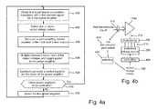
- Figure 4a depicts as a flow diagram an example embodiment of the operation of the apparatus 200.
- First transmission parameters associated with a first transmit signal for a first power amplifier 113a are obtained in block 400.
- the first transmission parameters may be used to select 402 one or more output voltages which may be needed for the first power amplifier 113a.
- the multi-level power source 202 is controlled 404 so that it would generate the one or more voltages selected in step 402.
- a multiplexer 208 may be controlled 406 so that it multiplexes between two or more of the voltages and supplies power to the first power amplifier 113a, wherein the first power amplifier 113a may amplify the first transmit signal.
- another control signal may be provided 408 to the power amplifier 113 to set the mode of the power amplifier.
- the above mentioned operations may be repeated 410 to other power amplifiers 113 as well.
- the procedure may continue 412 from the beginning. In other words, these operations may be continuous i.e. repeated again and again during the operation of the device 100.
- the level of the transmission signal to be amplified by that power amplifier 113 is measured to determine 404 the voltage level or voltage levels needed to be supplied to the power amplifier 113.
- Figure 4b depicts a diagram of the operation of the apparatus 200 according to an example embodiment, when controlling the supply voltage to be provided to a first power amplifier 113a.
- First transmission signals are provided 420 to the first power amplifier 113a.
- First transmission parameters associated with the first transmission signal are obtained 422.
- the (first) transmission parameters may be used to select 424 one or more output voltage values 426. These output voltage values 426 may be used in controlling 428 the multi-level power source 202.
- the multi-level power source 202 generates one or more output voltages 210 to be provided to the multiplexer 208, which may perform multiplexing between these output voltages and provide the output voltage 216 to the first power amplifier 113a which provides the voltage level needed by the first power amplifier 113a.
- the provided output voltage 216 may vary. It should be noted that although the terms first power amplifier 113a and first transmission signal were used here, similar operation may be applied to the other power amplifiers of the device 100 as well using transmission signals relating to the other power amplifiers.
- the selection of the voltage level for one power amplifier 113 may also be dependent on the operation mode or other criteria of one or more other power amplifiers.
- One example was already mentioned above, namely if one (or more) power amplifier 113 is set to operate in a constant supply voltage mode, it may be required that the reserved voltage output may not be used by the other power amplifiers 113.
- downlink and uplink transmissions are organized into frames of certain duration (10 ms).
- frames are divided into ten subframes, which may further be divided into two slots of 0.5 ms.
- a resource block is the smallest unit of resources that can be allocated to a user. In time domain a resource block is one slot long. The bandwidth of the resource block is 180 kHz. In frequency, resource blocks are composed of either 12 x 15 kHz subcarriers or 24 x 7.5 kHz subcarriers.
- Figure 5 shows a schematic block diagram of an exemplary apparatus or electronic device 50 depicted in Figure 6 , which may incorporate a transmitter according to an embodiment of the invention.
- the electronic device 50 may for example be a mobile terminal or user equipment of a wireless communication system. However, it would be appreciated that embodiments of the invention may be implemented within any electronic device or apparatus which may require transmission of radio frequency signals.
- the apparatus 50 may comprise a housing 30 for incorporating and protecting the device.
- the apparatus 50 further may comprise a display 32 in the form of a liquid crystal display.
- the display may be any suitable display technology suitable to display an image or video.
- the apparatus 50 may further comprise a keypad 34.
- any suitable data or user interface mechanism may be employed.
- the user interface may be implemented as a virtual keyboard or data entry system as part of a touch-sensitive display.
- the apparatus may comprise a microphone 36 or any suitable audio input which may be a digital or analogue signal input.
- the apparatus 50 may further comprise an audio output device which in embodiments of the invention may be any one of: an earpiece 38, speaker, or an analogue audio or digital audio output connection.
- the apparatus 50 may also comprise a battery 40 (or in other embodiments of the invention the device may be powered by any suitable mobile energy device such as solar cell, fuel cell or clockwork generator).
- the term battery discussed in connection with the embodiments may also be one of these mobile energy devices.
- the apparatus 50 may comprise a combination of different kinds of energy devices, for example a rechargeable battery and a solar cell.
- the apparatus may further comprise an infrared port 41 for short range line of sight communication to other devices.
- the apparatus 50 may further comprise any suitable short range communication solution such as for example a Bluetooth wireless connection or a USB/firewire wired connection.
- the apparatus 50 may comprise a controller 56 or processor for controlling the apparatus 50.
- the controller 56 may be connected to memory 58 which in embodiments of the invention may store both data and/or may also store instructions for implementation on the controller 56.
- the controller 56 may further be connected to codec circuitry 54 suitable for carrying out coding and decoding of audio and/or video data or assisting in coding and decoding carried out by the controller 56.
- the apparatus 50 may further comprise a card reader 48 and a smart card 46, for example a universal integrated circuit card (UICC) reader and UICC for providing user information and being suitable for providing authentication information for authentication and authorization of the user at a network.
- a card reader 48 and a smart card 46 for example a universal integrated circuit card (UICC) reader and UICC for providing user information and being suitable for providing authentication information for authentication and authorization of the user at a network.
- UICC universal integrated circuit card
- the apparatus 50 may comprise radio interface circuitry 52 connected to the controller and suitable for generating wireless communication signals for example for communication with a cellular communications network, a wireless communications system or a wireless local area network.
- the apparatus 50 may further comprise an antenna 108 connected to the radio interface circuitry 52 for transmitting radio frequency signals generated at the radio interface circuitry 52 to other apparatus(es) and for receiving radio frequency signals from other apparatus(es).
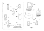
- the system 10 comprises multiple communication devices which can communicate through one or more networks.
- the system 10 may comprise any combination of wired and/or wireless networks including, but not limited to a wireless cellular telephone network (such as a GSM, UMTS, CDMA network etc.), a wireless local area network (WLAN) such as defined by any of the IEEE 802.x standards, a Bluetooth personal area network, an Ethernet local area network, a token ring local area network, a wide area network, and the Internet.
- a wireless cellular telephone network such as a GSM, UMTS, CDMA network etc.
- WLAN wireless local area network
- the system shown in Figure 7 shows a mobile telephone network 11 and a representation of the internet 28.
- Connectivity to the internet 28 may include, but is not limited to, long range wireless connections, short range wireless connections, and various wired connections including, but not limited to, telephone lines, cable lines, power lines, and similar communication pathways.
- the example communication devices shown in the system 10 may include, but are not limited to, an electronic device or apparatus 50, a combination of a personal digital assistant (PDA) and a mobile telephone 14, a PDA 16, an integrated messaging device (IMD) 18, a desktop computer 20, a notebook computer 22, a tablet computer.
- PDA personal digital assistant
- IMD integrated messaging device
- the apparatus 50 may be stationary or mobile when carried by an individual who is moving.
- the apparatus 50 may also be located in a mode of transport including, but not limited to, a car, a truck, a taxi, a bus, a train, a boat, an airplane, a bicycle, a motorcycle or any similar suitable mode of transport.
- Some or further apparatus may send and receive calls and messages and communicate with service providers through a wireless connection 25 to a base station 24.
- the base station 24 may be connected to a network server 26 that allows communication between the mobile telephone network 11 and the internet 28.
- the system may include additional communication devices and communication devices of various types.
- the communication devices may communicate using various transmission technologies including, but not limited to, code division multiple access (CDMA), global systems for mobile communications (GSM), universal mobile telecommunications system (UMTS), time divisional multiple access (TDMA), frequency division multiple access (FDMA), transmission control protocol-internet protocol (TCP-IP), short messaging service (SMS), multimedia messaging service (MMS), email, instant messaging service (IMS), Bluetooth, IEEE 802.11, Long Term Evolution wireless communication technique (LTE) and any similar wireless communication technology.
- CDMA code division multiple access
- GSM global systems for mobile communications
- UMTS universal mobile telecommunications system
- TDMA time divisional multiple access
- FDMA frequency division multiple access
- TCP-IP transmission control protocol-internet protocol
- SMS short messaging service
- MMS multimedia messaging service
- email instant messaging service
- Bluetooth Bluetooth
- LTE Long Term Evolution wireless communication technique
- LTE Long Term Evolution wireless communication technique
- HSDPA high-speed downlink packet access
- HSUPA high-speed uplink packet access
- a communications device involved in implementing various embodiments of the present invention may communicate using various media including, but not limited to, radio, infrared, laser, cable connections, and any suitable connection.
- various media including, but not limited to, radio, infrared, laser, cable connections, and any suitable connection.
- embodiments of the invention operating within a wireless communication device
- the invention as described above may be implemented as a part of any apparatus comprising a circuitry in which radio frequency signals are transmitted and/or received.
- embodiments of the invention may be implemented in a mobile phone, in a base station, in a computer such as a desktop computer or a tablet computer comprising radio frequency communication means (e.g. wireless local area network, cellular radio, etc.).
- radio frequency communication means e.g. wireless local area network, cellular radio, etc.
- Embodiments of the inventions may be practiced in various components such as integrated circuit modules, field-programmable gate arrays (FPGA), application specific integrated circuits (ASIC), microcontrollers, microprocessors, a combination of such modules.
- FPGA field-programmable gate arrays
- ASIC application specific integrated circuits
- microcontrollers microcontrollers
- microprocessors a combination of such modules.
- the design of integrated circuits is by and large a highly automated process. Complex and powerful software tools are available for converting a logic level design into a semiconductor circuit design ready to be etched and formed on a semiconductor substrate.
- Programs such as those provided by Synopsys, Inc. of Mountain View, California and Cadence Design, of San Jose, California automatically route conductors and locate components on a semiconductor chip using well established rules of design as well as libraries of pre stored design modules.
- the resultant design in a standardized electronic format (e.g., Opus, GDSII, or the like) may be transmitted to a semiconductor fabrication facility or "fab" for fabrication.
- a method comprising:
- the output voltages comprise a first output voltage, wherein the method comprises:
- an apparatus comprising:
- the output voltages comprise a first output voltage
- the apparatus is adapted to:
- the apparatus is adapted to look up one or more output voltage values from a lookup table on the basis of the first transmission parameters.
- the apparatus is a part of a wireless communication device.
- said at least one memory including computer program code, the at least one memory and the computer program code configured to, with the at least one processor, cause the apparatus to:
- the output voltages comprise a first output voltage
- said at least one memory including computer program code, the at least one memory and the computer program code configured to, with the at least one processor, cause the apparatus to:
- said at least one memory including computer program code, the at least one memory and the computer program code configured to, with the at least one processor, cause the apparatus to:
- a computer program product including one or more sequences of one or more instructions which, when executed by one or more processors, cause an apparatus to at least perform the following:
- an apparatus comprising:
Landscapes
- Engineering & Computer Science (AREA)
- Power Engineering (AREA)
- Microelectronics & Electronic Packaging (AREA)
- Amplifiers (AREA)
Priority Applications (4)
| Application Number | Priority Date | Filing Date | Title |
|---|---|---|---|
| EP15159312.6A EP3070842A1 (de) | 2015-03-17 | 2015-03-17 | Verfahren und vorrichtung für die stromversorgung eines verstärkers |
| PCT/FI2016/050155 WO2016146888A1 (en) | 2015-03-17 | 2016-03-14 | Method and apparatus for supplying power to an amplifier |
| US15/558,337 US10554187B2 (en) | 2015-03-17 | 2016-03-14 | Method and apparatus for supplying power to an amplifier |
| CN201680015970.6A CN107408925B (zh) | 2015-03-17 | 2016-03-14 | 向放大器供电的方法和装置 |
Applications Claiming Priority (1)
| Application Number | Priority Date | Filing Date | Title |
|---|---|---|---|
| EP15159312.6A EP3070842A1 (de) | 2015-03-17 | 2015-03-17 | Verfahren und vorrichtung für die stromversorgung eines verstärkers |
Publications (1)
| Publication Number | Publication Date |
|---|---|
| EP3070842A1 true EP3070842A1 (de) | 2016-09-21 |
Family
ID=52991448
Family Applications (1)
| Application Number | Title | Priority Date | Filing Date |
|---|---|---|---|
| EP15159312.6A Withdrawn EP3070842A1 (de) | 2015-03-17 | 2015-03-17 | Verfahren und vorrichtung für die stromversorgung eines verstärkers |
Country Status (4)
| Country | Link |
|---|---|
| US (1) | US10554187B2 (de) |
| EP (1) | EP3070842A1 (de) |
| CN (1) | CN107408925B (de) |
| WO (1) | WO2016146888A1 (de) |
Cited By (3)
| Publication number | Priority date | Publication date | Assignee | Title |
|---|---|---|---|---|
| WO2018073542A1 (fr) * | 2016-10-21 | 2018-04-26 | Worldcast Systems | Procede et dispositif d'optimisation de la puissance radiofrequence d'un emetteur de radiodiffusion fm |
| US10090808B1 (en) | 2017-03-30 | 2018-10-02 | Intel IP Corporation | Feed-forward envelope tracking |
| US20210234521A1 (en) * | 2020-01-24 | 2021-07-29 | Murata Manufacturing Co., Ltd. | Radio frequency circuit and communication device |
Families Citing this family (3)
| Publication number | Priority date | Publication date | Assignee | Title |
|---|---|---|---|---|
| US11601820B2 (en) * | 2017-01-27 | 2023-03-07 | Qualcomm Incorporated | Broadcast control channel for shared spectrum |
| US11515786B2 (en) * | 2019-08-28 | 2022-11-29 | Qualcomm Incorporated | Techniques for current sensing for single-inductor multiple-output (SIMO) regulators |
| US11870397B2 (en) * | 2022-02-18 | 2024-01-09 | Mediatek Inc. | Radio frequency module and associated method with envelope tracking power supply |
Citations (4)
| Publication number | Priority date | Publication date | Assignee | Title |
|---|---|---|---|---|
| EP0673112A1 (de) * | 1994-03-14 | 1995-09-20 | Matsushita Electronics Corporation | Leistungsverstärker und Verfahren dazu |
| US20070015472A1 (en) * | 2005-07-15 | 2007-01-18 | Simo Murtojarvi | Multimode transmitter, module, communication device and chip set |
| US20120075023A1 (en) * | 2010-08-25 | 2012-03-29 | Smarter Microelectronics | Hybrid reconfigurable multi-bands multi-modes power amplifier module |
| US20120200354A1 (en) * | 2011-02-07 | 2012-08-09 | Nujira Ltd | Apparatus and methods for envelope tracking calibration |
Family Cites Families (19)
| Publication number | Priority date | Publication date | Assignee | Title |
|---|---|---|---|---|
| US6157253A (en) * | 1999-09-03 | 2000-12-05 | Motorola, Inc. | High efficiency power amplifier circuit with wide dynamic backoff range |
| US7170341B2 (en) * | 2003-08-05 | 2007-01-30 | Motorola, Inc. | Low power consumption adaptive power amplifier |
| US20100001793A1 (en) * | 2006-12-12 | 2010-01-07 | Koninklijke Philips Electronics N.V. | High efficiency modulating rf amplifier |
| GB2465552B (en) * | 2008-11-18 | 2015-12-09 | Nujira Ltd | Power supply arrangement for multi-stage amplifier |
| CN101420205A (zh) * | 2008-11-28 | 2009-04-29 | 中山职业技术学院 | 一种数字音频功率放大器 |
| US9277501B2 (en) | 2010-02-08 | 2016-03-01 | Broadcom Corporation | Envelope tracker driven transmit beamforming |
| EP2561611B1 (de) * | 2010-04-19 | 2015-01-14 | RF Micro Devices, Inc. | Energieverwaltungssystem mit pseudo-hüllkurvenfolger |
| GB2480614B (en) | 2010-05-24 | 2017-04-12 | Snaptrack Inc | Switched arrangement for switched mode supply |
| US8598950B2 (en) * | 2010-12-14 | 2013-12-03 | Skyworks Solutions, Inc. | Apparatus and methods for capacitive load reduction |
| CN102684494B (zh) * | 2011-03-17 | 2014-10-29 | 中兴通讯股份有限公司 | 一种电源调制方法及电源调制器 |
| US8698558B2 (en) | 2011-06-23 | 2014-04-15 | Qualcomm Incorporated | Low-voltage power-efficient envelope tracker |
| GB2488380B (en) | 2011-06-24 | 2018-04-04 | Snaptrack Inc | Envelope tracking system for mimo |
| US8786373B2 (en) | 2012-02-21 | 2014-07-22 | Calogero D. Presti | Adjustable bypass circuit for a supply voltage for an amplifier |
| US8666339B2 (en) * | 2012-03-29 | 2014-03-04 | Triquint Semiconductor, Inc. | Radio frequency power amplifier with low dynamic error vector magnitude |
| US8884702B2 (en) * | 2012-09-14 | 2014-11-11 | Broadcom Corporation | Power amplifier with supply switching |
| US9166536B2 (en) * | 2012-10-30 | 2015-10-20 | Eta Devices, Inc. | Transmitter architecture and related methods |
| US9225302B2 (en) | 2012-12-03 | 2015-12-29 | Broadcom Corporation | Controlled power boost for envelope tracker |
| US8737940B1 (en) | 2013-02-28 | 2014-05-27 | Intel Mobile Communications GmbH | Envelope tracking system and method for calibrating a supply voltage of an envelope tracking power amplifier |
| US10193508B2 (en) * | 2014-04-17 | 2019-01-29 | Texas Instruments Incorporated | Multi-branch outphasing system and method |
-
2015
- 2015-03-17 EP EP15159312.6A patent/EP3070842A1/de not_active Withdrawn
-
2016
- 2016-03-14 WO PCT/FI2016/050155 patent/WO2016146888A1/en active Application Filing
- 2016-03-14 CN CN201680015970.6A patent/CN107408925B/zh not_active Expired - Fee Related
- 2016-03-14 US US15/558,337 patent/US10554187B2/en not_active Expired - Fee Related
Patent Citations (4)
| Publication number | Priority date | Publication date | Assignee | Title |
|---|---|---|---|---|
| EP0673112A1 (de) * | 1994-03-14 | 1995-09-20 | Matsushita Electronics Corporation | Leistungsverstärker und Verfahren dazu |
| US20070015472A1 (en) * | 2005-07-15 | 2007-01-18 | Simo Murtojarvi | Multimode transmitter, module, communication device and chip set |
| US20120075023A1 (en) * | 2010-08-25 | 2012-03-29 | Smarter Microelectronics | Hybrid reconfigurable multi-bands multi-modes power amplifier module |
| US20120200354A1 (en) * | 2011-02-07 | 2012-08-09 | Nujira Ltd | Apparatus and methods for envelope tracking calibration |
Cited By (9)
| Publication number | Priority date | Publication date | Assignee | Title |
|---|---|---|---|---|
| WO2018073542A1 (fr) * | 2016-10-21 | 2018-04-26 | Worldcast Systems | Procede et dispositif d'optimisation de la puissance radiofrequence d'un emetteur de radiodiffusion fm |
| FR3058013A1 (fr) * | 2016-10-21 | 2018-04-27 | Worldcast Systems | Procede et dispositif d'optimisation de la puissance radiofrequence d'un emetteur de radiodiffusion fm |
| CN110036581A (zh) * | 2016-10-21 | 2019-07-19 | 沃德卡斯特系统 | 用于优化调频广播发射机射频功率的方法和装置 |
| US10985851B2 (en) | 2016-10-21 | 2021-04-20 | Worldcast Systems | Method and device for optimizing the radiofrequency power of an FM radiobroadcasting transmitter |
| US10090808B1 (en) | 2017-03-30 | 2018-10-02 | Intel IP Corporation | Feed-forward envelope tracking |
| WO2018182880A1 (en) * | 2017-03-30 | 2018-10-04 | Intel IP Corporation | Feed-forward envelope tracking |
| US10862428B2 (en) | 2017-03-30 | 2020-12-08 | Apple Inc. | Feed-forward envelope tracking |
| US20210234521A1 (en) * | 2020-01-24 | 2021-07-29 | Murata Manufacturing Co., Ltd. | Radio frequency circuit and communication device |
| US11855594B2 (en) * | 2020-01-24 | 2023-12-26 | Murata Manufacturing Co., Ltd. | Radio frequency circuit and communication device |
Also Published As
| Publication number | Publication date |
|---|---|
| US10554187B2 (en) | 2020-02-04 |
| CN107408925A (zh) | 2017-11-28 |
| WO2016146888A1 (en) | 2016-09-22 |
| US20180069516A1 (en) | 2018-03-08 |
| CN107408925B (zh) | 2021-02-12 |
Similar Documents
| Publication | Publication Date | Title |
|---|---|---|
| US10554187B2 (en) | Method and apparatus for supplying power to an amplifier | |
| EP3059858A1 (de) | Verfahren und Vorrichtung für die Stromversorgung eines Verstärkers | |
| US11258408B2 (en) | Power envelope tracker and adjustable strength DC-DC converter | |
| CN115175336A (zh) | 资源确定方法、装置、终端、网络侧设备及存储介质 | |
| CN107251616B (zh) | 改善多用户识别模块设备中机会性包络跟踪的系统和方法 | |
| CN110431782B (zh) | 用于执行蜂窝通信的系统、装置和方法 | |
| US11388684B2 (en) | Method and apparatus for managing the maximum power on a secondary carrier | |
| US20240031119A1 (en) | Transmission direction determining method and apparatus, terminal, and network side device | |
| US20220159669A1 (en) | PDCCH Enhancement for Group Paging | |
| CN111566978B (zh) | 调节与更低阶互调产物共址的更高阶互调产物的方法和装置 | |
| US11677592B2 (en) | Transmitters and methods for operating the same | |
| US12082124B2 (en) | Method and apparatus for dynamic power sharing and managing the maximum power for a secondary carrier | |
| US10128795B2 (en) | Polar loop modulation techniques for wireless communication | |
| KR101640660B1 (ko) | 송신 신호 아티팩트 간격 저감 | |
| GB2524243A (en) | System and method for controlling a power amplifier | |
| US11601895B2 (en) | Method and apparatus for determining secondary cell group additional maximum power reduction and configured maximum power | |
| CN117641543B (zh) | 一种信号生成方法及装置 | |
| EP2785117B1 (de) | Downlink-signalverarbeitungsvorrichtung und verarbeitungsverfahren dafür | |
| US20220200535A1 (en) | Waveform-Tailored Average Power Tracking | |
| WO2022027292A1 (en) | Techniques for channel access by a user device with uplink (ul) cancellation in unlicensed bands | |
| KR20110087034A (ko) | 단말 및 그 제어방법 |
Legal Events
| Date | Code | Title | Description |
|---|---|---|---|
| PUAI | Public reference made under article 153(3) epc to a published international application that has entered the european phase |
Free format text: ORIGINAL CODE: 0009012 |
|
| AK | Designated contracting states |
Kind code of ref document: A1 Designated state(s): AL AT BE BG CH CY CZ DE DK EE ES FI FR GB GR HR HU IE IS IT LI LT LU LV MC MK MT NL NO PL PT RO RS SE SI SK SM TR |
|
| AX | Request for extension of the european patent |
Extension state: BA ME |
|
| 17P | Request for examination filed |
Effective date: 20170320 |
|
| RBV | Designated contracting states (corrected) |
Designated state(s): AL AT BE BG CH CY CZ DE DK EE ES FI FR GB GR HR HU IE IS IT LI LT LU LV MC MK MT NL NO PL PT RO RS SE SI SK SM TR |
|
| 17Q | First examination report despatched |
Effective date: 20170905 |
|
| STAA | Information on the status of an ep patent application or granted ep patent |
Free format text: STATUS: THE APPLICATION IS DEEMED TO BE WITHDRAWN |
|
| 18D | Application deemed to be withdrawn |
Effective date: 20180316 |