EP3070792B1 - Laser - Google Patents
Laser Download PDFInfo
- Publication number
- EP3070792B1 EP3070792B1 EP13899254.0A EP13899254A EP3070792B1 EP 3070792 B1 EP3070792 B1 EP 3070792B1 EP 13899254 A EP13899254 A EP 13899254A EP 3070792 B1 EP3070792 B1 EP 3070792B1
- Authority
- EP
- European Patent Office
- Prior art keywords
- region
- mode selection
- reflective mode
- laser
- phase shift
- Prior art date
- Legal status (The legal status is an assumption and is not a legal conclusion. Google has not performed a legal analysis and makes no representation as to the accuracy of the status listed.)
- Active
Links
Images



Classifications
-
- H—ELECTRICITY
- H01—ELECTRIC ELEMENTS
- H01S—DEVICES USING THE PROCESS OF LIGHT AMPLIFICATION BY STIMULATED EMISSION OF RADIATION [LASER] TO AMPLIFY OR GENERATE LIGHT; DEVICES USING STIMULATED EMISSION OF ELECTROMAGNETIC RADIATION IN WAVE RANGES OTHER THAN OPTICAL
- H01S5/00—Semiconductor lasers
- H01S5/10—Construction or shape of the optical resonator, e.g. extended or external cavity, coupled cavities, bent-guide, varying width, thickness or composition of the active region
- H01S5/1003—Waveguide having a modified shape along the axis, e.g. branched, curved, tapered, voids
- H01S5/1007—Branched waveguides
-
- H—ELECTRICITY
- H01—ELECTRIC ELEMENTS
- H01S—DEVICES USING THE PROCESS OF LIGHT AMPLIFICATION BY STIMULATED EMISSION OF RADIATION [LASER] TO AMPLIFY OR GENERATE LIGHT; DEVICES USING STIMULATED EMISSION OF ELECTROMAGNETIC RADIATION IN WAVE RANGES OTHER THAN OPTICAL
- H01S5/00—Semiconductor lasers
- H01S5/10—Construction or shape of the optical resonator, e.g. extended or external cavity, coupled cavities, bent-guide, varying width, thickness or composition of the active region
- H01S5/14—External cavity lasers
- H01S5/141—External cavity lasers using a wavelength selective device, e.g. a grating or etalon
- H01S5/142—External cavity lasers using a wavelength selective device, e.g. a grating or etalon which comprises an additional resonator
-
- H—ELECTRICITY
- H01—ELECTRIC ELEMENTS
- H01S—DEVICES USING THE PROCESS OF LIGHT AMPLIFICATION BY STIMULATED EMISSION OF RADIATION [LASER] TO AMPLIFY OR GENERATE LIGHT; DEVICES USING STIMULATED EMISSION OF ELECTROMAGNETIC RADIATION IN WAVE RANGES OTHER THAN OPTICAL
- H01S5/00—Semiconductor lasers
- H01S5/02—Structural details or components not essential to laser action
- H01S5/028—Coatings ; Treatment of the laser facets, e.g. etching, passivation layers or reflecting layers
-
- H—ELECTRICITY
- H01—ELECTRIC ELEMENTS
- H01S—DEVICES USING THE PROCESS OF LIGHT AMPLIFICATION BY STIMULATED EMISSION OF RADIATION [LASER] TO AMPLIFY OR GENERATE LIGHT; DEVICES USING STIMULATED EMISSION OF ELECTROMAGNETIC RADIATION IN WAVE RANGES OTHER THAN OPTICAL
- H01S5/00—Semiconductor lasers
- H01S5/30—Structure or shape of the active region; Materials used for the active region
- H01S5/3013—AIIIBV compounds
-
- H—ELECTRICITY
- H01—ELECTRIC ELEMENTS
- H01S—DEVICES USING THE PROCESS OF LIGHT AMPLIFICATION BY STIMULATED EMISSION OF RADIATION [LASER] TO AMPLIFY OR GENERATE LIGHT; DEVICES USING STIMULATED EMISSION OF ELECTROMAGNETIC RADIATION IN WAVE RANGES OTHER THAN OPTICAL
- H01S5/00—Semiconductor lasers
- H01S5/02—Structural details or components not essential to laser action
- H01S5/0206—Substrates, e.g. growth, shape, material, removal or bonding
- H01S5/021—Silicon based substrates
-
- H—ELECTRICITY
- H01—ELECTRIC ELEMENTS
- H01S—DEVICES USING THE PROCESS OF LIGHT AMPLIFICATION BY STIMULATED EMISSION OF RADIATION [LASER] TO AMPLIFY OR GENERATE LIGHT; DEVICES USING STIMULATED EMISSION OF ELECTROMAGNETIC RADIATION IN WAVE RANGES OTHER THAN OPTICAL
- H01S5/00—Semiconductor lasers
- H01S5/02—Structural details or components not essential to laser action
- H01S5/026—Monolithically integrated components, e.g. waveguides, monitoring photo-detectors, drivers
- H01S5/0265—Intensity modulators
-
- H—ELECTRICITY
- H01—ELECTRIC ELEMENTS
- H01S—DEVICES USING THE PROCESS OF LIGHT AMPLIFICATION BY STIMULATED EMISSION OF RADIATION [LASER] TO AMPLIFY OR GENERATE LIGHT; DEVICES USING STIMULATED EMISSION OF ELECTROMAGNETIC RADIATION IN WAVE RANGES OTHER THAN OPTICAL
- H01S5/00—Semiconductor lasers
- H01S5/02—Structural details or components not essential to laser action
- H01S5/028—Coatings ; Treatment of the laser facets, e.g. etching, passivation layers or reflecting layers
- H01S5/0287—Facet reflectivity
-
- H—ELECTRICITY
- H01—ELECTRIC ELEMENTS
- H01S—DEVICES USING THE PROCESS OF LIGHT AMPLIFICATION BY STIMULATED EMISSION OF RADIATION [LASER] TO AMPLIFY OR GENERATE LIGHT; DEVICES USING STIMULATED EMISSION OF ELECTROMAGNETIC RADIATION IN WAVE RANGES OTHER THAN OPTICAL
- H01S5/00—Semiconductor lasers
- H01S5/06—Arrangements for controlling the laser output parameters, e.g. by operating on the active medium
- H01S5/062—Arrangements for controlling the laser output parameters, e.g. by operating on the active medium by varying the potential of the electrodes
- H01S5/0625—Arrangements for controlling the laser output parameters, e.g. by operating on the active medium by varying the potential of the electrodes in multi-section lasers
- H01S5/06255—Controlling the frequency of the radiation
- H01S5/06256—Controlling the frequency of the radiation with DBR-structure
Definitions
- the present invention relates to the field of communications technologies, and specifically, to a laser.
- optical communications In last two decades, optical communications technologies have achieved rapid development.
- information is modulated into light to form an optical signal, the optical signal is transmitted to a destination by using an optical fiber, and the information carried in the optical signal is demodulated after arrival at the destination.
- Optical communications has advantages of a high speed and low crosstalk, and therefore is a development direction of a fixed network in future.
- the laser is a device that employs a stimulated emission theory to enable light in some stimulated substance to be amplified or emitted in an oscillating manner.
- laser power is output from one port.
- an additional beam splitting structure is required at an output end, or multiple same lasers are required.
- WO-A1-2007/107187 discloses a laser resonant cavity configured to generate a laser beam comprising an active gain region with a high-reflectivity coating, an optical branching region, and N comb like reflectors, where N is greater than or equal to 2.
- the active gain region is located on a first substrate, and the optical branching region and the N comb like reflectors are located on a second substrate arranged in proximity to the first substrate.
- the optical branching region comprises N+1 ports, one port being optically coupled with the active gain region, and the other N ports being optically coupled with the N comb like reflectors respectively; and wherein each comb like reflector comprises two ports, one optically coupled with the optical branching region, and the other configured to output the laser beam so that the laser is capable of emitting N laser beams at a same wavelength.
- US-A1-2013/016423 discloses a laser having a resonant cavity comprising a semiconductor optical amplifier with a highly reflective surface and including phase adjusters in each of the branches between an optical branching region and a plurality of respective mode selection adjacent reflectors. Laser outputs at a same wavelength are obtained from each of the output ports of the adjacent reflectors.
- the semiconductor optical amplifier is butt coupled to the substrate on which the optical branching region and adjacent reflectors are situated.
- Embodiments of the present invention provide a laser.
- the laser provided by the embodiments of the present invention includes a substrate and a resonant cavity; the resonant cavity includes a highly reflective surface, an active gain region, a first phase shift region configured to tune a spectral position of a longitudinal mode of the resonant cavity, an optical branching region, and N reflective mode selection regions, where the resonant cavity is configured to generate a laser beam, and N is greater than or equal to 2;
- the active gain region, the first phase shift region, the optical branching region, and the N reflective mode selection regions are coupled to the substrate;
- the active gain region includes two ports, and the two ports of the active gain region are optically coupled with the highly reflective surface and the first phase shift region respectively;
- the first phase shift region includes two ports, and the two ports of the first phase shift region are optically coupled with the active gain region and the optical branching region respectively;
- the optical branching region includes N+1 ports, one port of the optical branching region is optically coupled
- the active gain region includes a III-V compound and is configured to generate spontaneous emission light under the effect of forward bias;
- the first phase shift region is configured to tune a spectral position of a longitudinal mode of the resonant cavity by changing a refractive index of the first phase shift region;
- the optical branching region is configured to perform power splitting on light from the first phase shift region and output N beams of light obtained after power splitting to the N reflective mode selection regions, and is further configured to combine light from the N reflective mode selection regions and output light obtained after light combination to the first phase shift region;
- each of the N reflective mode selection regions include a transflective structure, a reflection peak emerges periodically on a spectral reflectance curve of each reflective mode selection region as a light wavelength changes continually, and the spectral reflectance curves of the N reflective mode selection regions have reflection peaks on a same wavelength position, where the spectral reflectance curve is a spectral line that uses the light wavelength or a light frequency as a horizontal axis and a reflectivity as a vertical
- the laser may further include at least one second phase shift region; the at least one second phase shift region is coupled to the substrate; at least one reflective mode selection region of the N reflective mode selection regions is optically coupled with the optical branching region by using the at least one second phase shift region; and the at least one second phase shift region is configured to adjust a phase of light passing through the at least one second phase shift region.
- the laser provided by the embodiments of the present invention includes a substrate and a resonant cavity.
- the resonant cavity further includes a highly reflective surface, where a reflectivity of the highly reflective surface is greater than peak reflectivities of the N reflective mode selection regions, so that laser beams are output from the N reflective mode selection regions. Because the laser naturally includes at least two reflective mode selection regions, at least two laser beams are output. According to the laser provided by the embodiments of the present invention, one laser can output two laser beams or even multiple laser beams; therefore, laser beam generation efficiency is high and average costs for generating a single laser beam are accordingly reduced.
- Coupled and “connection” mainly refer to a direct or indirect physical connection
- optical coupling mainly refers to a direct or indirect connection relationship in an optical path.
- coupling and optical coupling may coexist in many cases, and therefore the two are not mutually exclusive.
- the invention is defined in claim 1.
- the active gain region includes a III-V compound and is configured to generate spontaneous emission light under the effect of forward bias;
- the first phase shift region is configured to tune a spectral position of a longitudinal mode of the resonant cavity by changing a refractive index of the first phase shift region;
- the optical branching region is configured to perform power splitting on light from the first phase shift region and output N beams of light obtained after power splitting to the N reflective mode selection regions, and is further configured to combine light from the N reflective mode selection regions and output light obtained after light combination to the first phase shift region;
- each of the N reflective mode selection regions include a transflective structure, a reflection peak emerges periodically on a spectral reflectance curve of each reflective mode selection region as a light wavelength or frequency changes continually, and the spectral reflectance curves of the N reflective mode selection regions have reflection peaks at a same wavelength position, where the spectral reflectance curve is a spectral line that uses the light wavelength as a horizontal axis and a reflectivity as a vertical axi
- reflectivities of spectral reflectance curves of at least two reflective mode selection regions of the N reflective mode selection regions are mutually different at the wavelength or frequency position.
- the laser further includes N antireflective surfaces, and the N antireflective surfaces are optically coupled respectively with the ports that are of the N reflective mode selection regions and that are configured to output the laser beam.
- the laser further includes N optical power tuning regions and N antireflective surfaces, where each optical power tuning region has two ports, one port is optically coupled with the port that is of one reflective mode selection region and that is configured to output the laser beam, the other port is optically coupled with one antireflective surface, and the optical power tuning region is configured to tune power of the laser beam emitted from the reflective mode selection region.
- the laser further includes N optical power tuning regions, N bent waveguide structures, and N antireflective surfaces, where each optical power tuning region and each bent waveguide structure have two ports, one port of each optical power tuning region is optically coupled with the port that is of one reflective mode selection region and that is configured to output the laser beam, the other port of each optical power tuning region is optically coupled with one bent waveguide structure, one port of each bent waveguide structure is optically coupled with one optical power tuning region, and the other port of each bent waveguide structure is optically coupled with one antireflective surface; and the optical power tuning region is configured to tune power of the laser beam emitted from the reflective mode selection region.
- the laser further includes at least one second phase shift region; the at least one second phase shift region is coupled to the substrate; at least one reflective mode selection region of the N reflective mode selection regions is optically coupled with the optical branching region by using the at least one second phase shift region; and the at least one second phase shift region is configured to adjust a phase of light passing through the at least one second phase shift region.
- the laser in accordance with the invention includes a spot adjustment region; the first phase shift region is optically coupled with the optical branching region by using the spot adjustment region; and the spot adjustment region is configured to adjust a spot in light passing through the spot adjustment region.
- the substrate includes a first substrate and a second substrate that are separated, and an empty slot is disposed between the first substrate and the second substrate; the active gain region and the first phase shift region are coupled on the first substrate, and the optical branching region and the N reflective mode selection regions are coupled on the second substrate; and the spot adjustment region is specifically a lens and disposed in the empty slot.
- the reflectivity of the highly reflective surface is greater than 50%.
- the reflective mode selection region is a superstructured sampled grating distributed Bragg reflector, or a microring structure, or a sampled fiber Bragg grating structure.
- the optical branching region is a Y-type waveguide or a 1x2 multimode interferometer; and if N is greater than 2, the optical branching region is a 1xN multimode interferometer.
- the present invention provides a laser that uses a "highly reflective surface+active gain region+first phase shift region+optical branching region+N reflective mode selection regions" structure and can emit narrow linewidth and wavelength-tunable laser beams. Meanwhile, the laser can output the laser beams from multiple emission ports with no need of additionally adding a beam splitting structure.
- reflectivities of reflective mode selection regions may be set to different values, and accordingly, emission ports of the reflective mode selection regions may output laser beams of different power.
- an antireflective surface and a bent waveguide may be added at a laser-beam output end, so as to suppress end face reflection at the laser-beam emission port.
- a power tuning region may be further added to independently implement functions of flexibly tuning and turning off laser power at each laser-beam emission port.
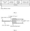
- FIG. 1 is a side view of a laser according to an embodiment of the present invention.
- FIG. 1 is merely a schematic diagram, and is used to explain implementation details of the embodiment of the present invention and may slightly differ from a real object.
- An active gain region, a first phase shift region, an optical branching region, and a reflective mode selection region in the figure are optically coupled directly or indirectly. These regions may be connected directly, or may have spacing among them, or may also be optically coupled by using a waveguide or another optical connecting device, and even they may be directly coupled with another optical device, which is not limited in the embodiment of the present invention.
- FIG. 2 is a top view of the laser in FIG. 1 .
- a substrate is not shown in FIG. 2 .
- the active gain region includes two ports, one port is optically coupled with a highly reflective surface, and the other port is optically coupled with the first phase shift region.
- the active gain region is a region that includes a III-V semiconductor structure and that is used to generate spontaneous emission light.
- a III-V semiconductor mainly refers to a compound of a group III element and a group V element in the periodic table of elements, is also referred to as a compound semiconductor or a III-V compound, and mainly includes gallium arsenide (GaAs), indium phosphide (InP), gallium nitride, and the like.
- the active gain region includes positive and negative electrodes, configured to implement forward bias.
- the III-V semiconductor generates wide-spectrum spontaneous emission light under the effect of forward bias.
- the first phase shift region may tune a spectral position of a longitudinal mode of a resonant cavity of the laser by changing a refractive index of the first phase shift region.
- the longitudinal mode of the resonant cavity of the laser is related to a cavity length of the resonant cavity and a refractive index of a transmission medium.
- the spectral position of the longitudinal mode of the resonant cavity may be tuned by changing the refractive index of the transmission medium, so as to finally obtain a required laser frequency.
- the refractive index of the first phase shift region may be changed in many manners: according to a specific material of the first phase shift region, a thermo-optic tuning method may be used, that is, a change of the refractive index of the first phase shift region is adjusted by using a temperature change; electrical injection tuning may be used, that is, the refractive index of the first phase shift region is changed by means of forming an injected carrier by using an applied electric field; and piezoelectric tuning may also be used.
- the optical branching region is configured to combine and split light, and specifically may be a Y-type waveguide or a 1xN multimode interferometer.
- the reflective mode selection region includes a transflective structure, where a reflectivity is less than a reflectivity of the highly reflective surface. It should be noted that a reflection peak emerges periodically on a spectral reflectance curve of each reflective mode selection region of reflective mode selection regions as a light wavelength or frequency changes continually.
- the reflectivity of the highly reflective surface is greater than the reflectivity of the reflective mode selection region, where "greater than” herein refers to that the reflectivity of the highly reflective surface is greater than a peak value of the reflection peak of the reflective mode selection region. Because the reflectivity of the highly reflective surface is greater than the reflectivity of the reflective mode selection region, a laser beam with a majority of power is emitted from an emission port of the reflective mode selection region.
- a laser beam is emitted only from the reflective mode selection region.
- a part of a laser beam may also be emitted from the highly reflective surface, and this part of the laser beam may be used for monitoring, and the like.
- FIG. 3 is a view of spectral reflectance curves of the two reflective mode selection regions in FIG. 1 and FIG. 2 .
- the spectral reflectance curves are represented by a solid line and a dotted line respectively in FIG. 3 . It can be seen that the two reflective mode selection regions have different spectral reflectance curves.
- a cycle of a reflection peak of each spectral reflectance curve is different, and for different reflective mode selection regions, peak values of reflection peaks may be the same, or may be different.
- Reflection peaks of spectral reflectance curves of different reflective mode selection regions may coincide at a wavelength.
- Reflection peaks of the spectral reflectance curves of the two reflective mode selection regions in FIG. 3 coincide at a wavelength of 1555 nanometers.
- 1555-nanometer light generated by means of spontaneous emission is reflected, and the reflected light is amplified due to stimulated emission when passing through an active gain region. Therefore, the 1555-nanometer light is oscillated back and forth in a resonant cavity, and a stable 1555-nanomater laser beam is finally output.
- free spectral ranges corresponding to the two reflective mode selection regions are 4.64 nanometers and 5 nanometers respectively. According to a Vernier effect, it can be obtained by calculation that a tunable wavelength range that can be achieved by the laser is 64.44 nanometers, and the wavelength range can cover a C-band wavelength range. Due to such a difference between the free spectral ranges of the two reflective mode selection regions, it may be implemented that reflection peaks completely coincide and overlap at only one wavelength position within the C-band range. As shown in FIG. 3 , the reflection peaks completely coincide and overlap only at the 1555-nanometer wavelength.
- Reflected light generated by the reflective mode selection regions is returned to the optical branching region, and is emitted in a combined manner through a port connecting the optical branching region and the first phase shift region.
- a spectrum of the combined light is a result of interference and overlapping of beams of the reflected light.
- multiple reflective mode selection regions as a whole have the spectral reflectance curve shown in FIG. 4 .
- a reflection peak is highest at a 1555-nanometer wavelength, and peak values of reflection peaks of other levels are suppressed and decreased after light combination, so that light with the 1555-nanometer wavelength has a smallest threshold gain in a resonant cavity between a highly reflective surface and the reflective mode selection region, thereby implementing single longitudinal mode lasing.
- a laser beam generated by the resonant cavity is emitted from two ports of the reflective mode selection regions respectively.
- reflectivities of the two reflective mode selection regions may be different, for example, a reflectivity of one reflective mode selection region may be twice a reflectivity of the other reflective mode selection region, optical power of a laser beam emitted from one reflective mode selection region is 1/2 of optical power of a laser beam emitted from the other reflective mode selection region.
- unbalanced output of emission power from two different emission ports may be implemented by setting reflectivities of different reflective mode selection regions.
- gratings of different reflectivities may be formed by using different coupling factor or different sampling cycles.
- a reflectivity when the reflective mode selection region is a microring structure, a reflectivity may be controlled by controlling spacing between a ring in the microring structure and a corresponding coupling waveguide, and the reflectivity may also be controlled by controlling a coupling factor for coupling a waveguide to a ring.
- an overlapping position of the reflective mode selection regions may be adjusted by means of heating tuning, or electrical injection tuning, or piezoelectric tuning, thereby implementing tuning of a wavelength.
- a quantity of the reflective mode selection regions is exemplarily 2, and actually may be 3, 4, or even more, which is not limited in this embodiment of the present invention. Meanwhile, reflectivities of the reflective mode selection regions may be set to be different. In this way, output laser power of the reflective mode selection regions may also be different. Therefore, one laser may output multiple laser beams of different power, so as to meet different application scenarios.
- a laser provided by an embodiment of the present invention may further include an antireflective surface, which may be configured to suppress end face reflection.
- the laser may further include a bent waveguide, configured to suppress end face reflection.
- the antireflective surface may be an antireflective film, a grating with a low reflectivity and a high transmittance, a gradient waveguide structure, or the like.
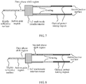
- FIG. 6 shows a laser provided by an embodiment of the present invention.
- an optical branching region is specifically a 1x2 multimode interferometer MMI
- a reflective mode selection region is specifically a grating.
- the grating may be specifically a superstructured sampled grating distributed Bragg reflector (Superstructured sampled grating Distributed Bragg Reflector, SSGDBR), and may also be another appropriate grating structure.
- a reflectivity of a highly reflective surface is greater than 50%, for example, may be 95%.
- a peak value of a reflectivity of the SSGDBR may be 7%, 14%, 20%, or the like, and reflectivities of two SSGDBRs may be the same, or may be different.
- a laser further includes an optical power tuning region.
- the optical power tuning region may be configured to independently tune, amplify, or turn off emission power of a laser beam from a reflective mode selection region.
- an injection current is formed by applying a forward or reverse bias voltage on optical power tuning, where a size of the injection current determines times of gain amplification of an optical gain region. If a forward bias voltage is applied, an emitted laser beam is amplified; and if a reverse bias voltage is applied, an emitted laser beam is decreased, and even is completely absorbed, thereby implementing power tuning of the emitted laser beam.
- a laser further includes a second phase shift region, configured to adjust a phase of light passing through the second phase shift region, so that when the light returns from reflective mode selection regions to an optical branching region for light combination, phases of light returned from each reflective mode selection region are consistent, thereby generating a phase overlapping effect.
- a refractive index of the second phase shift region may be adjusted by means of heating tuning, electrical injection tuning, or piezoelectric tuning, so as to achieve an effect of phase adjustment of light.
- the refractive index of the second phase shift region may be adjusted gradually.
- FIG. 8 exemplarily shows an example that the reflective mode selection region is a grating, and a quantity of reflective mode selection regions is 2. Actually, when there are multiple reflective mode selection regions, there may be multiple second phase shift regions that are respectively configured to modulate phases of light from the reflective mode selection regions.
- a laser further includes a spot adjustment region, configured to adjust a spot size and shape.
- the spot adjustment region may be configured to adjust a spot in a resonant cavity, so that light from a first phase shift region may be better coupled to an optical branching region.
- the spot adjustment region is specifically a lens.
- the substrate in the embodiments of the present invention includes two pieces of substrates: a first substrate and a second substrate respectively, as shown in FIG. 10 .
- the substrate in the embodiments of the present invention may be a III-V compound substrate, or may be a silicon substrate.
- a highly reflective surface, an active gain region, an optical branching region, and a reflective mode selection region that are in the embodiments of the present invention are necessary structures; an antireflective surface, a bent waveguide, an optical power tuning region, a second phase shift region are optional structures, and these optional structures may be used in any combination.
- the optical branching region may be a Y-type waveguide, or may be a 1xN multimode interferometer.
- a laser provided by the embodiments of the present invention includes a substrate and a resonant cavity.
- the resonant cavity further includes a highly reflective surface, where a reflectivity of the highly reflective surface is greater than reflectivities of the N reflective mode selection regions, so that laser beams are output from the N reflective mode selection regions. Because the laser naturally includes at least two reflective mode selection regions, at least two laser beams are output. According to the laser provided by the embodiments of the present invention, one laser can output two laser beams or even multiple laser beams; therefore, laser beam generation efficiency is high and average costs for generating a single laser beam are accordingly reduced.
- a quantity of reflective mode selection regions of a laser may be greater than 2, and for a longitudinal mode selected from multiple reflective mode selection regions, a line width is narrower, and frequency uniformity is better.
- reflectivities of reflective mode selection regions of a laser may be different, so as to implement unbalanced output of laser beams from multiple ports, thereby meeting different application scenarios.
- a laser provided by the embodiments of the present invention may include an antireflective surface and a bent waveguide, which can effectively suppress end face reflection, enhance transmittance of an emitted laser beam, and improve laser beam emission efficiency.
- a laser provided by the embodiments of the present invention may include at least one second phase shift region, configured to flexibly adjust a phase of light, so that phases of light of each reflective mode selection region are the same during light combination, and an overlapping effect is generated, thereby improving laser beam generation efficiency.
- a substrate of a laser provided by the embodiments of the present invention includes a first substrate and a second substrate that are separated, where an active gain region and a first phase shift region are coupled on the first substrate, an optical branching region and N reflective mode selection regions are coupled on the second substrate, and the first phase shift region is optically coupled with the optical branching region by using a lens.
- the laser using two substrates features a significantly larger resonant cavity length than an ordinary laser, and therefore, more excellent narrow linewidth performance may be obtained.
Landscapes
- Physics & Mathematics (AREA)
- Condensed Matter Physics & Semiconductors (AREA)
- General Physics & Mathematics (AREA)
- Electromagnetism (AREA)
- Optics & Photonics (AREA)
- Semiconductor Lasers (AREA)
- Optical Modulation, Optical Deflection, Nonlinear Optics, Optical Demodulation, Optical Logic Elements (AREA)
Claims (10)
- Laser, wobei der Laser ein Substrat und einen Resonanzhohlraum umfasst;
wobei der Resonanzhohlraum eine hochreflektierende Oberfläche, eine aktive Verstärkungsregion, eine erste Phasenverschiebungsregion, die ausgelegt ist zum Abstimmen einer spektralen Position einer Longitudinalmode des Resonanzhohlraums, eine optische Verzweigungsregion und N reflektierende Modenselektionsregionen umfasst, wobei der Resonanzhohlraum ausgelegt ist zum Erzeugen eines Laserstrahls und N größer oder gleich 2 ist;
die aktive Verstärkungsregion, die erste Phasenverschiebungsregion, die optische Verzweigungsregion und die N reflektierenden Modenselektionsregionen mit dem Substrat gekoppelt sind;
die aktive Verstärkungsregion zwei Zugänge umfasst und die zwei Zugänge der aktiven Verstärkungsregion jeweils mit der optisch hochreflektierenden Oberfläche und der ersten Phasenverschiebungsregion gekoppelt sind;
die erste Phasenverschiebungsregion zwei Zugänge umfasst und die zwei Zugänge der ersten Phasenverschiebungsregion jeweils optisch mit der aktiven Verstärkungsregion und der optischen Verzweigungsregion gekoppelt sind;
die optische Verzweigungsregion N+1 Zugänge umfasst, wobei ein Zugang der optischen Verzweigungsregion optisch mit der ersten Phasenverschiebungsregion gekoppelt ist und die anderen N Zugänge der optischen Phasenverschiebungsregion jeweils optisch mit den N reflektierenden Modenselektionsregionen gekoppelt sind; jede reflektierende Modenselektionsregion der N reflektierenden Modenselektionsregionen zwei Zugänge umfasst, wobei ein Zugang optisch mit der optischen Verzweigungsregion gekoppelt ist und der andere Zugang dafür ausgelegt ist, den Laserstrahl auszugeben, so dass der Laser in der Lage ist, N Laserstrahlen mit einer selben Wellenlänge zu emittieren; und
eine Reflektivität der hochreflektierenden Oberfläche größer als Spitzenreflektivitäten der N reflektierenden Modenselektionsregionen ist;
wobei der Laser ferner eine Fleckeinstellungsregion umfasst;
die optische Phasenverschiebungsregion unter Verwendung der Fleckeinstellungsregion optisch mit der optischen Verzweigungsregion gekoppelt ist; und
die Fleckeinstellungsregion dafür ausgelegt ist, eine Fleckgröße und -form von durch die Fleckeinstellungsregion hindurchgehendem Licht einzustellen,
wobei das Substrat ein erstes Substrat und ein zweites Substrat umfasst, die getrennt sind, und ein leerer Schlitz zwischen dem ersten Substrat und dem zweiten Substrat angeordnet ist;
die aktive Verstärkungsregion und die erste Phasenverschiebungsregion auf dem ersten Substrat gekoppelt sind und die optische Verzweigungsregion und die N reflektierenden Modenselektionsregionen auf dem zweiten Substrat gekoppelt sind; und
die Fleckeinstellungsregion insbesondere eine Linse ist, die in dem leeren Schlitz angeordnet ist. - Laser nach Anspruch 1, wobei
die aktive Verstärkungsregion eine III-V-Verbindung umfasst und ausgelegt ist zum Erzeugen von Licht spontaner Emission unter Einwirkung einer Vorwärtsvorspannung;
die erste Phasenverschiebungsregion ausgelegt ist zum Abstimmen einer spektralen Position einer Longitudinalmode des Resonanzhohlraums durch Ändern eines Brechungsindizes der ersten Phasenverschiebungsregion;
die erste Verzweigungsregion ausgelegt ist zum Durchführen von Leistungsaufspaltung an Licht von der ersten Phasenverschiebungsregion und zum Ausgeben von N Strahlen von Licht, das nach der Leistungsaufspaltung in die N reflektierenden Modenselektionsregionen erhalten wird, und ferner ausgelegt ist zum Kombinieren von Licht von den N reflektierenden Modenselektionsregionen und zum Ausgeben von Licht, das nach Lichtkombination erhalten wird, zur ersten Phasenverschiebungsregion; und
jede der N reflektierenden Modenselektionsregionen eine transflektierende Struktur umfasst, wobei bei sich kontinuierlich ändernder Lichtwellenlänge periodisch eine Reflexionsspitze auf einer spektralen Reflektivitätskurve von jeder reflektierenden Modenselektionsregion auftaucht und die spektralen Reflektivitätskurven der N Modenselektionsregionen bei einer selben Wellenlängenposition Reflexionsspitzen aufweisen, wobei die spektrale Reflektivitätskurve eine Spektrallinie ist, die die Lichtwellenlänge oder eine Lichtfrequenz als eine Horizontalachse und eine Reflektivität als eine Vertikalachse verwendet und die ein Variationsmerkmal der Reflektivität mit der Lichtwellenlänge wiedergibt. - Laser nach Anspruch 2, wobei sich Spitzenreflektivitäten der spektralen Reflektivitätskurven von mindestens zwei reflektierenden Modenselektionsregionen der N reflektierenden Modenselektionsregionen gegenseitig bei der Wellenlängenposition unterscheiden.
- Laser nach einem der Ansprüche 1 bis 3, wobei
der Laser ferner N Antireflexoberflächen umfasst und die N Antireflexoberflächen jeweils optisch mit den Zugängen gekoppelt sind, die zu den N reflektierenden Modenselektionsregionen gehören und die ausgelegt sind zum Ausgeben des Laserstrahls. - Laser nach einem der Ansprüche 1 bis 3, wobei
der Laser ferner N optische Leistungsabstimmregionen und N Antireflexoberflächen umfasst, wobei jede optische Leistungsabstimmregion zwei Zugänge aufweist, wobei ein Zugang optisch mit dem Zugang gekoppelt ist, der zu einer reflektierenden Modenselektionsregion gehört und der ausgelegt ist zum Ausgeben des Laserstrahls, wobei der andere Zugang optisch mit einer Antireflexoberfläche gekoppelt ist, und die optische Leistungsabstimmregion dafür ausgelegt ist, die Leistung des von der reflektierenden Modenselektionsregion emittierten Laserstrahls abzustimmen. - Laser nach einem der Ansprüche 1 bis 3, wobei
der Laser ferner N optische Leistungsabstimmregionen, N gebogene Wellenleiterstrukturen und N Antireflexoberflächen umfasst, wobei jede optische Leistungsabstimmregion und jede gebogene Wellenleiterstruktur zwei Zugänge aufweist, wobei ein Zugang von jeder optischen Leistungsabstimmregion optisch mit dem Zugang gekoppelt ist, der zu einer reflektierenden Modenselektionsregion gehört und der ausgelegt ist zum Ausgeben des Laserstrahls, wobei der andere Zugang von jeder optischen Leistungsabstimmregion optisch mit einer gebogenen Wellenleiterstruktur gekoppelt ist, wobei ein Zugang von jeder gebogenen Wellenleiterstruktur optisch mit einer optischen Leistungsabstimmregion gekoppelt ist und der andere Zugang von jeder gebogenen Wellenleiterstruktur optisch mit einer Antireflexoberfläche gekoppelt ist; und die optische Leistungsabstimmregion dafür ausgelegt ist, die Leistung des von der reflektierenden Modenselektionsregion emittierten Laserstrahls abzustimmen. - Laser nach einem der Ansprüche 1 bis 6, wobei
der Laser ferner mindestens eine zweite Phasenverschiebungsregion umfasst; die mindestens eine zweite Phasenverschiebungsregion mit dem zweiten Substrat gekoppelt ist;
mindestens eine reflektierende Modenselektionsregion der N reflektierenden Modenselektionsregionen unter Verwendung der mindestens einen zweiten Phasenverschiebungsregion optisch mit der optischen Verzweigungsregion gekoppelt ist; und
die mindestens eine zweite Phasenverschiebungsregion ausgelegt ist zum Einstellen einer Phase von Licht, das durch die mindestens eine zweite Phasenverschiebungsregion hindurchgeht. - Laser nach einem der Ansprüche 1 bis 7, wobei
die Reflektivität der hochreflektierenden Oberfläche größer als 50% ist. - Laser nach einem der Ansprüche 1 bis 8, wobei
die reflektierende Modenselektionsregion eine gesampelte Faser-Bragg-GitterStruktur oder ein superstrukturierter gesampelter verteilter Bragg-Reflektor oder eine Mikroringstruktur ist. - Laser nach einem der Ansprüche 1 bis 9, wobei
wenn N gleich 2 ist, die optische Verzweigungsregion ein Y-Wellenleiter oder ein 1x2-Multimodeninterferometer ist; und
wenn N größer als 2 ist, die optische Verzweigungsregion ein 1xN-Multimodeninterferometer ist.
Applications Claiming Priority (1)
| Application Number | Priority Date | Filing Date | Title |
|---|---|---|---|
| PCT/CN2013/089244 WO2015085544A1 (zh) | 2013-12-12 | 2013-12-12 | 一种激光器 |
Publications (3)
| Publication Number | Publication Date |
|---|---|
| EP3070792A1 EP3070792A1 (de) | 2016-09-21 |
| EP3070792A4 EP3070792A4 (de) | 2016-12-07 |
| EP3070792B1 true EP3070792B1 (de) | 2018-02-14 |
Family
ID=53370503
Family Applications (1)
| Application Number | Title | Priority Date | Filing Date |
|---|---|---|---|
| EP13899254.0A Active EP3070792B1 (de) | 2013-12-12 | 2013-12-12 | Laser |
Country Status (4)
| Country | Link |
|---|---|
| US (1) | US9735540B2 (de) |
| EP (1) | EP3070792B1 (de) |
| CN (1) | CN105144509B (de) |
| WO (1) | WO2015085544A1 (de) |
Families Citing this family (7)
| Publication number | Priority date | Publication date | Assignee | Title |
|---|---|---|---|---|
| EP3088855B1 (de) * | 2015-04-28 | 2020-10-21 | IMEC vzw | Kompaktes interferometer |
| CN105811241B (zh) * | 2016-04-20 | 2018-07-24 | 太原理工大学 | 一种双反馈的单片集成激光器芯片 |
| CN108075354A (zh) * | 2016-11-14 | 2018-05-25 | 中国科学院苏州纳米技术与纳米仿生研究所 | 窄线宽激光器 |
| EP3535821A1 (de) * | 2016-12-08 | 2019-09-11 | Huawei Technologies Co., Ltd. | Laser mit einer steuerbaren ausgangswellenlänge |
| JP7385158B2 (ja) * | 2020-05-25 | 2023-11-22 | 日本電信電話株式会社 | 波長可変レーザダイオード |
| US20230378718A1 (en) * | 2020-10-13 | 2023-11-23 | Nippon Telegraph And Telephone Corporation | Tunable Light Source and Control Method |
| EP4662169A1 (de) * | 2023-02-06 | 2025-12-17 | Ramot at Tel-Aviv University Ltd. | Laser auf der basis eines dielektrischen resonators mit gas oder plasma bei populationsinversion |
Family Cites Families (12)
| Publication number | Priority date | Publication date | Assignee | Title |
|---|---|---|---|---|
| US5913000A (en) * | 1995-12-29 | 1999-06-15 | Doerr; Christopher Richard | Method and apparatus for guiding optical signals |
| JPH11307847A (ja) * | 1998-04-24 | 1999-11-05 | Ishikawajima Harima Heavy Ind Co Ltd | 2波長同時発振レーザ装置 |
| US6728279B1 (en) | 1999-05-17 | 2004-04-27 | Interuniversitair Microelektronica Centrum | Widely wavelength tunable integrated semiconductor device and method for widely tuning semiconductor devices |
| US20030152116A1 (en) * | 2002-02-12 | 2003-08-14 | Hsien-Kuei Liao | Power-equalizing multi-channel fiber laser array |
| WO2007107187A1 (en) * | 2006-03-23 | 2007-09-27 | Pirelli & C. S.P.A. | Integrated laser optical source with active and passive sections formed in distinct substrates |
| GB2448162A (en) | 2007-04-03 | 2008-10-08 | Bookham Technology Plc | Tunable semiconductor laser |
| US8615025B2 (en) | 2009-10-13 | 2013-12-24 | Skorpios Technologies, Inc. | Method and system for hybrid integration of a tunable laser |
| US8467122B2 (en) * | 2011-07-13 | 2013-06-18 | Oracle America, Inc. | Hybrid laser source with ring-resonator reflector |
| CN103733448B (zh) * | 2011-08-10 | 2016-08-17 | 富士通株式会社 | 半导体光元件 |
| WO2014022971A1 (zh) * | 2012-08-07 | 2014-02-13 | 华为技术有限公司 | 外调制激光器、无源光通信设备及系统 |
| CN103098488A (zh) * | 2012-10-29 | 2013-05-08 | 华为技术有限公司 | 波长可调激光器、无源光网络系统和设备 |
| WO2014107537A1 (en) * | 2013-01-02 | 2014-07-10 | Packet Photonics, Inc. | Tunable u-laser transmitter with integrated mach-zehnder modulator |
-
2013
- 2013-12-12 EP EP13899254.0A patent/EP3070792B1/de active Active
- 2013-12-12 WO PCT/CN2013/089244 patent/WO2015085544A1/zh not_active Ceased
- 2013-12-12 CN CN201380002437.2A patent/CN105144509B/zh active Active
-
2016
- 2016-06-09 US US15/177,853 patent/US9735540B2/en active Active
Non-Patent Citations (1)
| Title |
|---|
| None * |
Also Published As
| Publication number | Publication date |
|---|---|
| US20160294158A1 (en) | 2016-10-06 |
| CN105144509A (zh) | 2015-12-09 |
| CN105144509B (zh) | 2018-01-12 |
| EP3070792A1 (de) | 2016-09-21 |
| EP3070792A4 (de) | 2016-12-07 |
| WO2015085544A1 (zh) | 2015-06-18 |
| US9735540B2 (en) | 2017-08-15 |
Similar Documents
| Publication | Publication Date | Title |
|---|---|---|
| US9735540B2 (en) | Laser | |
| US9762034B2 (en) | Tunable laser source, optical transmitter, and optical transmitter and receiver module | |
| US9705282B2 (en) | Multi-wavelength laser light source and wavelength multiplexing communication system | |
| KR100916311B1 (ko) | 이중 결합 링 공진기를 이용한 파장 가변 레이저 다이오드 | |
| US9436022B2 (en) | Modulated light source | |
| US20170353001A1 (en) | Tunable laser | |
| JP6425631B2 (ja) | 半導体レーザおよびこれを備える光集積光源 | |
| US8467122B2 (en) | Hybrid laser source with ring-resonator reflector | |
| CN108141006B (zh) | 半导体激光器装置 | |
| CN104937791A (zh) | 激光装置、光调制装置以及光半导体元件 | |
| US12500392B2 (en) | Wavelength control of multi-wavelength laser | |
| US20140254617A1 (en) | Tunable laser diode device with amzi-fp filter | |
| CN117498135A (zh) | 大范围波长调谐激光器 | |
| WO2016082541A1 (zh) | 一种大范围调谐激光器及其调谐方法 | |
| JP7662615B2 (ja) | モノリシックに集積されたInPの電気光学的に調整可能なリングレーザー、レーザーデバイス、及び対応する方法 | |
| US8995480B2 (en) | Tunable laser module | |
| KR20140089925A (ko) | 공진기, 파장 가변 필터 및 파장 가변 레이저 다이오드 | |
| JP5001239B2 (ja) | 半導体波長可変レーザ | |
| Bowers | Integrated microwave photonics | |
| US20250015563A1 (en) | Systems and methods for beam combination of tapered diode lasers and amplifiers | |
| JP6540097B2 (ja) | 波長可変レーザ装置 | |
| CN117878722B (zh) | 注入锁定窄线宽硅基端面耦合外腔激光器以及控制方法 | |
| JP5058087B2 (ja) | 波長可変半導体レーザ | |
| CN103384950B (zh) | 激光器波导装置 | |
| JPS62136890A (ja) | 半導体レ−ザ装置 |
Legal Events
| Date | Code | Title | Description |
|---|---|---|---|
| PUAI | Public reference made under article 153(3) epc to a published international application that has entered the european phase |
Free format text: ORIGINAL CODE: 0009012 |
|
| 17P | Request for examination filed |
Effective date: 20160615 |
|
| AK | Designated contracting states |
Kind code of ref document: A1 Designated state(s): AL AT BE BG CH CY CZ DE DK EE ES FI FR GB GR HR HU IE IS IT LI LT LU LV MC MK MT NL NO PL PT RO RS SE SI SK SM TR |
|
| AX | Request for extension of the european patent |
Extension state: BA ME |
|
| A4 | Supplementary search report drawn up and despatched |
Effective date: 20161109 |
|
| RIC1 | Information provided on ipc code assigned before grant |
Ipc: H01S 5/028 20060101ALN20161103BHEP Ipc: H01S 5/0625 20060101ALN20161103BHEP Ipc: H01S 5/02 20060101ALN20161103BHEP Ipc: H01S 5/026 20060101ALN20161103BHEP Ipc: H01S 5/14 20060101AFI20161103BHEP |
|
| DAX | Request for extension of the european patent (deleted) | ||
| REG | Reference to a national code |
Ref country code: DE Ref legal event code: R079 Ref document number: 602013033226 Country of ref document: DE Free format text: PREVIOUS MAIN CLASS: H01S0003082000 Ipc: H01S0005140000 |
|
| GRAP | Despatch of communication of intention to grant a patent |
Free format text: ORIGINAL CODE: EPIDOSNIGR1 |
|
| STAA | Information on the status of an ep patent application or granted ep patent |
Free format text: STATUS: GRANT OF PATENT IS INTENDED |
|
| RIC1 | Information provided on ipc code assigned before grant |
Ipc: H01S 5/0625 20060101ALN20170619BHEP Ipc: H01S 5/028 20060101ALN20170619BHEP Ipc: H01S 5/14 20060101AFI20170619BHEP Ipc: H01S 5/02 20060101ALN20170619BHEP Ipc: H01S 5/026 20060101ALN20170619BHEP |
|
| INTG | Intention to grant announced |
Effective date: 20170704 |
|
| GRAS | Grant fee paid |
Free format text: ORIGINAL CODE: EPIDOSNIGR3 |
|
| GRAA | (expected) grant |
Free format text: ORIGINAL CODE: 0009210 |
|
| STAA | Information on the status of an ep patent application or granted ep patent |
Free format text: STATUS: THE PATENT HAS BEEN GRANTED |
|
| AK | Designated contracting states |
Kind code of ref document: B1 Designated state(s): AL AT BE BG CH CY CZ DE DK EE ES FI FR GB GR HR HU IE IS IT LI LT LU LV MC MK MT NL NO PL PT RO RS SE SI SK SM TR |
|
| REG | Reference to a national code |
Ref country code: GB Ref legal event code: FG4D |
|
| REG | Reference to a national code |
Ref country code: CH Ref legal event code: EP |
|
| REG | Reference to a national code |
Ref country code: IE Ref legal event code: FG4D |
|
| REG | Reference to a national code |
Ref country code: DE Ref legal event code: R096 Ref document number: 602013033226 Country of ref document: DE Ref country code: AT Ref legal event code: REF Ref document number: 970448 Country of ref document: AT Kind code of ref document: T Effective date: 20180315 |
|
| REG | Reference to a national code |
Ref country code: NL Ref legal event code: MP Effective date: 20180214 |
|
| REG | Reference to a national code |
Ref country code: AT Ref legal event code: MK05 Ref document number: 970448 Country of ref document: AT Kind code of ref document: T Effective date: 20180214 |
|
| PG25 | Lapsed in a contracting state [announced via postgrant information from national office to epo] |
Ref country code: NL Free format text: LAPSE BECAUSE OF FAILURE TO SUBMIT A TRANSLATION OF THE DESCRIPTION OR TO PAY THE FEE WITHIN THE PRESCRIBED TIME-LIMIT Effective date: 20180214 Ref country code: LT Free format text: LAPSE BECAUSE OF FAILURE TO SUBMIT A TRANSLATION OF THE DESCRIPTION OR TO PAY THE FEE WITHIN THE PRESCRIBED TIME-LIMIT Effective date: 20180214 Ref country code: ES Free format text: LAPSE BECAUSE OF FAILURE TO SUBMIT A TRANSLATION OF THE DESCRIPTION OR TO PAY THE FEE WITHIN THE PRESCRIBED TIME-LIMIT Effective date: 20180214 Ref country code: NO Free format text: LAPSE BECAUSE OF FAILURE TO SUBMIT A TRANSLATION OF THE DESCRIPTION OR TO PAY THE FEE WITHIN THE PRESCRIBED TIME-LIMIT Effective date: 20180514 Ref country code: HR Free format text: LAPSE BECAUSE OF FAILURE TO SUBMIT A TRANSLATION OF THE DESCRIPTION OR TO PAY THE FEE WITHIN THE PRESCRIBED TIME-LIMIT Effective date: 20180214 Ref country code: FI Free format text: LAPSE BECAUSE OF FAILURE TO SUBMIT A TRANSLATION OF THE DESCRIPTION OR TO PAY THE FEE WITHIN THE PRESCRIBED TIME-LIMIT Effective date: 20180214 Ref country code: CY Free format text: LAPSE BECAUSE OF FAILURE TO SUBMIT A TRANSLATION OF THE DESCRIPTION OR TO PAY THE FEE WITHIN THE PRESCRIBED TIME-LIMIT Effective date: 20180214 |
|
| PG25 | Lapsed in a contracting state [announced via postgrant information from national office to epo] |
Ref country code: SE Free format text: LAPSE BECAUSE OF FAILURE TO SUBMIT A TRANSLATION OF THE DESCRIPTION OR TO PAY THE FEE WITHIN THE PRESCRIBED TIME-LIMIT Effective date: 20180214 Ref country code: LV Free format text: LAPSE BECAUSE OF FAILURE TO SUBMIT A TRANSLATION OF THE DESCRIPTION OR TO PAY THE FEE WITHIN THE PRESCRIBED TIME-LIMIT Effective date: 20180214 Ref country code: GR Free format text: LAPSE BECAUSE OF FAILURE TO SUBMIT A TRANSLATION OF THE DESCRIPTION OR TO PAY THE FEE WITHIN THE PRESCRIBED TIME-LIMIT Effective date: 20180515 Ref country code: BG Free format text: LAPSE BECAUSE OF FAILURE TO SUBMIT A TRANSLATION OF THE DESCRIPTION OR TO PAY THE FEE WITHIN THE PRESCRIBED TIME-LIMIT Effective date: 20180514 Ref country code: RS Free format text: LAPSE BECAUSE OF FAILURE TO SUBMIT A TRANSLATION OF THE DESCRIPTION OR TO PAY THE FEE WITHIN THE PRESCRIBED TIME-LIMIT Effective date: 20180214 Ref country code: AT Free format text: LAPSE BECAUSE OF FAILURE TO SUBMIT A TRANSLATION OF THE DESCRIPTION OR TO PAY THE FEE WITHIN THE PRESCRIBED TIME-LIMIT Effective date: 20180214 |
|
| PG25 | Lapsed in a contracting state [announced via postgrant information from national office to epo] |
Ref country code: AL Free format text: LAPSE BECAUSE OF FAILURE TO SUBMIT A TRANSLATION OF THE DESCRIPTION OR TO PAY THE FEE WITHIN THE PRESCRIBED TIME-LIMIT Effective date: 20180214 Ref country code: IT Free format text: LAPSE BECAUSE OF FAILURE TO SUBMIT A TRANSLATION OF THE DESCRIPTION OR TO PAY THE FEE WITHIN THE PRESCRIBED TIME-LIMIT Effective date: 20180214 Ref country code: EE Free format text: LAPSE BECAUSE OF FAILURE TO SUBMIT A TRANSLATION OF THE DESCRIPTION OR TO PAY THE FEE WITHIN THE PRESCRIBED TIME-LIMIT Effective date: 20180214 Ref country code: PL Free format text: LAPSE BECAUSE OF FAILURE TO SUBMIT A TRANSLATION OF THE DESCRIPTION OR TO PAY THE FEE WITHIN THE PRESCRIBED TIME-LIMIT Effective date: 20180214 Ref country code: RO Free format text: LAPSE BECAUSE OF FAILURE TO SUBMIT A TRANSLATION OF THE DESCRIPTION OR TO PAY THE FEE WITHIN THE PRESCRIBED TIME-LIMIT Effective date: 20180214 |
|
| REG | Reference to a national code |
Ref country code: DE Ref legal event code: R097 Ref document number: 602013033226 Country of ref document: DE |
|
| PG25 | Lapsed in a contracting state [announced via postgrant information from national office to epo] |
Ref country code: SM Free format text: LAPSE BECAUSE OF FAILURE TO SUBMIT A TRANSLATION OF THE DESCRIPTION OR TO PAY THE FEE WITHIN THE PRESCRIBED TIME-LIMIT Effective date: 20180214 Ref country code: SK Free format text: LAPSE BECAUSE OF FAILURE TO SUBMIT A TRANSLATION OF THE DESCRIPTION OR TO PAY THE FEE WITHIN THE PRESCRIBED TIME-LIMIT Effective date: 20180214 Ref country code: CZ Free format text: LAPSE BECAUSE OF FAILURE TO SUBMIT A TRANSLATION OF THE DESCRIPTION OR TO PAY THE FEE WITHIN THE PRESCRIBED TIME-LIMIT Effective date: 20180214 Ref country code: DK Free format text: LAPSE BECAUSE OF FAILURE TO SUBMIT A TRANSLATION OF THE DESCRIPTION OR TO PAY THE FEE WITHIN THE PRESCRIBED TIME-LIMIT Effective date: 20180214 |
|
| PLBE | No opposition filed within time limit |
Free format text: ORIGINAL CODE: 0009261 |
|
| STAA | Information on the status of an ep patent application or granted ep patent |
Free format text: STATUS: NO OPPOSITION FILED WITHIN TIME LIMIT |
|
| 26N | No opposition filed |
Effective date: 20181115 |
|
| PG25 | Lapsed in a contracting state [announced via postgrant information from national office to epo] |
Ref country code: SI Free format text: LAPSE BECAUSE OF FAILURE TO SUBMIT A TRANSLATION OF THE DESCRIPTION OR TO PAY THE FEE WITHIN THE PRESCRIBED TIME-LIMIT Effective date: 20180214 |
|
| REG | Reference to a national code |
Ref country code: CH Ref legal event code: PL |
|
| PG25 | Lapsed in a contracting state [announced via postgrant information from national office to epo] |
Ref country code: MC Free format text: LAPSE BECAUSE OF FAILURE TO SUBMIT A TRANSLATION OF THE DESCRIPTION OR TO PAY THE FEE WITHIN THE PRESCRIBED TIME-LIMIT Effective date: 20180214 Ref country code: LU Free format text: LAPSE BECAUSE OF NON-PAYMENT OF DUE FEES Effective date: 20181212 |
|
| REG | Reference to a national code |
Ref country code: IE Ref legal event code: MM4A |
|
| REG | Reference to a national code |
Ref country code: BE Ref legal event code: MM Effective date: 20181231 |
|
| PG25 | Lapsed in a contracting state [announced via postgrant information from national office to epo] |
Ref country code: IE Free format text: LAPSE BECAUSE OF NON-PAYMENT OF DUE FEES Effective date: 20181212 Ref country code: FR Free format text: LAPSE BECAUSE OF NON-PAYMENT OF DUE FEES Effective date: 20181231 |
|
| PG25 | Lapsed in a contracting state [announced via postgrant information from national office to epo] |
Ref country code: BE Free format text: LAPSE BECAUSE OF NON-PAYMENT OF DUE FEES Effective date: 20181231 |
|
| PG25 | Lapsed in a contracting state [announced via postgrant information from national office to epo] |
Ref country code: LI Free format text: LAPSE BECAUSE OF NON-PAYMENT OF DUE FEES Effective date: 20181231 Ref country code: CH Free format text: LAPSE BECAUSE OF NON-PAYMENT OF DUE FEES Effective date: 20181231 |
|
| PG25 | Lapsed in a contracting state [announced via postgrant information from national office to epo] |
Ref country code: MT Free format text: LAPSE BECAUSE OF NON-PAYMENT OF DUE FEES Effective date: 20181212 |
|
| PG25 | Lapsed in a contracting state [announced via postgrant information from national office to epo] |
Ref country code: TR Free format text: LAPSE BECAUSE OF FAILURE TO SUBMIT A TRANSLATION OF THE DESCRIPTION OR TO PAY THE FEE WITHIN THE PRESCRIBED TIME-LIMIT Effective date: 20180214 |
|
| PG25 | Lapsed in a contracting state [announced via postgrant information from national office to epo] |
Ref country code: PT Free format text: LAPSE BECAUSE OF FAILURE TO SUBMIT A TRANSLATION OF THE DESCRIPTION OR TO PAY THE FEE WITHIN THE PRESCRIBED TIME-LIMIT Effective date: 20180214 |
|
| PG25 | Lapsed in a contracting state [announced via postgrant information from national office to epo] |
Ref country code: MK Free format text: LAPSE BECAUSE OF NON-PAYMENT OF DUE FEES Effective date: 20180214 Ref country code: HU Free format text: LAPSE BECAUSE OF FAILURE TO SUBMIT A TRANSLATION OF THE DESCRIPTION OR TO PAY THE FEE WITHIN THE PRESCRIBED TIME-LIMIT; INVALID AB INITIO Effective date: 20131212 |
|
| PG25 | Lapsed in a contracting state [announced via postgrant information from national office to epo] |
Ref country code: IS Free format text: LAPSE BECAUSE OF FAILURE TO SUBMIT A TRANSLATION OF THE DESCRIPTION OR TO PAY THE FEE WITHIN THE PRESCRIBED TIME-LIMIT Effective date: 20180614 |
|
| PGFP | Annual fee paid to national office [announced via postgrant information from national office to epo] |
Ref country code: DE Payment date: 20251104 Year of fee payment: 13 |
|
| PGFP | Annual fee paid to national office [announced via postgrant information from national office to epo] |
Ref country code: GB Payment date: 20251030 Year of fee payment: 13 |