EP3068008B1 - Améliorations apportées ou relatives à des convertisseurs de puissance à courant continu à haute tension - Google Patents
Améliorations apportées ou relatives à des convertisseurs de puissance à courant continu à haute tension Download PDFInfo
- Publication number
- EP3068008B1 EP3068008B1 EP15275062.6A EP15275062A EP3068008B1 EP 3068008 B1 EP3068008 B1 EP 3068008B1 EP 15275062 A EP15275062 A EP 15275062A EP 3068008 B1 EP3068008 B1 EP 3068008B1
- Authority
- EP
- European Patent Office
- Prior art keywords
- conducting
- current
- protection element
- semiconductor
- electrical assembly
- Prior art date
- Legal status (The legal status is an assumption and is not a legal conclusion. Google has not performed a legal analysis and makes no representation as to the accuracy of the status listed.)
- Active
Links
- 239000004065 semiconductor Substances 0.000 claims description 99
- 230000000712 assembly Effects 0.000 claims description 10
- 238000000429 assembly Methods 0.000 claims description 10
- 238000004891 communication Methods 0.000 claims description 9
- 238000004146 energy storage Methods 0.000 claims description 7
- 230000000903 blocking effect Effects 0.000 claims description 3
- 239000003990 capacitor Substances 0.000 description 10
- 230000005540 biological transmission Effects 0.000 description 3
- 238000006243 chemical reaction Methods 0.000 description 3
- 239000004020 conductor Substances 0.000 description 2
- 238000000034 method Methods 0.000 description 2
- 230000002457 bidirectional effect Effects 0.000 description 1
- 230000000694 effects Effects 0.000 description 1
- 238000000605 extraction Methods 0.000 description 1
- 230000004907 flux Effects 0.000 description 1
- 238000003780 insertion Methods 0.000 description 1
- 230000037431 insertion Effects 0.000 description 1
- 238000002955 isolation Methods 0.000 description 1
- 238000012544 monitoring process Methods 0.000 description 1
- 230000002000 scavenging effect Effects 0.000 description 1
- 230000001960 triggered effect Effects 0.000 description 1
Images


Classifications
-
- H—ELECTRICITY
- H02—GENERATION; CONVERSION OR DISTRIBUTION OF ELECTRIC POWER
- H02M—APPARATUS FOR CONVERSION BETWEEN AC AND AC, BETWEEN AC AND DC, OR BETWEEN DC AND DC, AND FOR USE WITH MAINS OR SIMILAR POWER SUPPLY SYSTEMS; CONVERSION OF DC OR AC INPUT POWER INTO SURGE OUTPUT POWER; CONTROL OR REGULATION THEREOF
- H02M1/00—Details of apparatus for conversion
- H02M1/32—Means for protecting converters other than automatic disconnection
-
- H—ELECTRICITY
- H02—GENERATION; CONVERSION OR DISTRIBUTION OF ELECTRIC POWER
- H02J—CIRCUIT ARRANGEMENTS OR SYSTEMS FOR SUPPLYING OR DISTRIBUTING ELECTRIC POWER; SYSTEMS FOR STORING ELECTRIC ENERGY
- H02J3/00—Circuit arrangements for ac mains or ac distribution networks
- H02J3/36—Arrangements for transfer of electric power between ac networks via a high-tension dc link
-
- H—ELECTRICITY
- H02—GENERATION; CONVERSION OR DISTRIBUTION OF ELECTRIC POWER
- H02M—APPARATUS FOR CONVERSION BETWEEN AC AND AC, BETWEEN AC AND DC, OR BETWEEN DC AND DC, AND FOR USE WITH MAINS OR SIMILAR POWER SUPPLY SYSTEMS; CONVERSION OF DC OR AC INPUT POWER INTO SURGE OUTPUT POWER; CONTROL OR REGULATION THEREOF
- H02M7/00—Conversion of ac power input into dc power output; Conversion of dc power input into ac power output
- H02M7/42—Conversion of dc power input into ac power output without possibility of reversal
- H02M7/44—Conversion of dc power input into ac power output without possibility of reversal by static converters
- H02M7/48—Conversion of dc power input into ac power output without possibility of reversal by static converters using discharge tubes with control electrode or semiconductor devices with control electrode
- H02M7/483—Converters with outputs that each can have more than two voltages levels
- H02M7/4835—Converters with outputs that each can have more than two voltages levels comprising two or more cells, each including a switchable capacitor, the capacitors having a nominal charge voltage which corresponds to a given fraction of the input voltage, and the capacitors being selectively connected in series to determine the instantaneous output voltage
-
- Y—GENERAL TAGGING OF NEW TECHNOLOGICAL DEVELOPMENTS; GENERAL TAGGING OF CROSS-SECTIONAL TECHNOLOGIES SPANNING OVER SEVERAL SECTIONS OF THE IPC; TECHNICAL SUBJECTS COVERED BY FORMER USPC CROSS-REFERENCE ART COLLECTIONS [XRACs] AND DIGESTS
- Y02—TECHNOLOGIES OR APPLICATIONS FOR MITIGATION OR ADAPTATION AGAINST CLIMATE CHANGE
- Y02E—REDUCTION OF GREENHOUSE GAS [GHG] EMISSIONS, RELATED TO ENERGY GENERATION, TRANSMISSION OR DISTRIBUTION
- Y02E60/00—Enabling technologies; Technologies with a potential or indirect contribution to GHG emissions mitigation
- Y02E60/60—Arrangements for transfer of electric power between AC networks or generators via a high voltage DC link [HVCD]
Definitions
- This invention relates to an electrical assembly for use in a limb portion of a converter limb within a high voltage direct current (HVDC) power converter.
- HVDC high voltage direct current
- alternating current (AC) electrical power is converted to high voltage direct current (DC) power for transmission via overhead lines and/or undersea cables.
- DC direct current
- This conversion reduces the cost per kilometre of the lines and/or cables, and is therefore cost-effective when power needs to be transmitted over a long distance.
- the high voltage DC electrical power is converted back to AC electrical power before being distributed to local networks.
- HVDC power converters are required at each interface between AC and DC networks to effect the required conversion between AC power and DC power.
- Each switch cell has bidirectional power semiconductor switches, which can be actuated, having a controlled, unidirectional current conducting direction and a capacitive energy store.
- the inductances of the first and second partial inverter systems are serially connected, with a phase connection being formed by the connection points of the inductances of the first and second partial inverter systems.
- a short-circuit element is connected in parallel to each switch cell to the connection poles thereof in order to contain a fault current in a partial inverter system and an interrupting element is serially connected between the associated short-circuit element and the switch cell.
- WO 2013/083414 describes a method for eliminating an arc driven by at least one phase voltage source of a converter circuit, comprising monitoring a state variable of the converter circuit for a predeterminable threshold value of the state variable to detect an arc, and actuating at least one of a plurality of actuatable power semiconductor switches of the converter unit upon detecting a discrepancy between the state variable and the predeterminable threshold value.
- an electrical assembly for use in a limb portion of a converter limb within a HVDC power converter, the electrical assembly comprising at least one switching assembly including one or more semiconductor switches, the or each semiconductor switch being selectively switchable between conducting and non-conducting conditions, the or each semiconductor switch in the conducting condition allowing current to flow through the said semiconductor switch in a first forward direction and thereby through the said switching assembly in the same forward direction, the or each switching assembly having a bypass protection circuit connected in parallel therewith, the or each bypass protection circuit including a first semiconductor protection element selectively switchable between conducting and non-conducting conditions,the or each said first semiconductor protection element while in the conducting condition providing a first current-conducting path in the forward direction to divert current flowing in the forward direction through the switching assembly away from the switching assembly.
- bypass protection circuit permits the electrical assembly of the invention to handle obscure and unusual fault currents that flow in the forward direction.
- forward fault currents might arise because of a disturbance on an AC side of a power converter in which the electrical assembly of the invention is installed, because of a failure in the control hardware of such a power converter, or because of some other erroneous event.
- the first semiconductor protection element is able to react quickly to the presence of a forward fault current which might otherwise, damage, impair or endanger the associated switching assembly if not diverted away therefrom.
- the first semiconductor protection element can be switched readily and remotely back into a non-conducting condition following the removal of the fault and resulting forward fault current, e.g. without the need to secure physical access to the bypass protection circuit which might otherwise be extremely difficult and/or necessitate the costly interruption of operation of a power converter in which the electrical assembly of the invention is located.
- one or more bypass protection circuits includes a second semiconductor protection element arranged to provide a second current-conducting path in a second reverse direction opposite the forward direction to divert current flowing in a reverse direction through the corresponding switching assembly away from the said switching assembly.
- the second semiconductor protection element of one or more bypass protection circuits is or includes a passive current check element that continually permits current to flow therethrough in the reverse direction while continually blocking the flow of current therethrough in the forward direction.
- Providing such a second semiconductor protection element assists in ensuring permanent bypass protection in the reverse direction without the need to detect a reverse fault current or initiate a switching operation, and so helps to ensure that the electrical assembly of the invention is able to deal with conventional, and more numerous DC faults, i.e. faults that give rise to a fault current flowing in the reverse direction.
- the second semiconductor protection element of one or more bypass protection circuits may be or include a semiconductor switch selectively switchable between conducting and non-conducting conditions.
- a second semiconductor protection element that is selectively switchable between conducting and non-conducting conditions allows use of such a second semiconductor protection element to be limited to the handling of DC faults only, i.e. faults that give rise to a fault current flowing in the reverse direction. Accordingly, during normal operation of a power converter in which the electrical assembly of the invention is, in use, installed, such a second semiconductor protection element can be switched into a non-conducting condition so that sharing of current between the second semiconductor protection element and the associated switching assembly is prevented. Preventing such current sharing allows for the selection of a second semiconductor protection element with lower performance characteristics, i.e. slower switching, that would otherwise be the case, and so reduces the cost of the second semiconductor protection element. In addition, the duty cycle of the second semiconductor protection element is lower than would be the case if current sharing occurred, and so the life expectancy of the second semiconductor protection element is increased.
- the first semiconductor protection element of one or more bypass protection circuits is connected in series with a current-limiting reactor.
- Having a reactor connected in series with a respective first semiconductor protection element helps to limit the rate of rise of current flowing through the first semiconductor protection element when it is switched into a conducting condition, and thereby helps to prevent damage to the first semiconductor protection element.
- Such an arrangement also helps to prevent spurious switching of the first semiconductor protection element into its conducting condition, e.g. as may otherwise be occasioned by an excess change in forward voltage across the first semiconductor protection element during switching within the associated switching assembly.
- the first semiconductor protection element of one or more bypass protection circuits is connected in parallel with a snubber circuit.
- Arranging a snubber circuit in such a manner helps to dampen voltage variations across the said first semiconductor protection element while it is in its non-conducting condition, and also to help limit a voltage overshoot when the first semiconductor protection element is switched from its conducting condition to its non-conducting condition.
- each first semiconductor protection element is arranged in operative communication with a local control unit programmed to at least switch a said first semiconductor protection element into its conducting condition.
- Such an arrangement desirably achieves selective switching of the or each said first semiconductor protection element.
- the or each local control unit may be arranged to draw power from an adjacent component within the electrical assembly.
- Having the or each local control unit so arranged permits the or each said local control unit to operate independently, e.g. when a higher-level control unit is de-energised.
- each local control unit is further programmed to act in accordance with an operating condition of a higher-level control unit with which it is, in use, arranged in operative communication.
- An electrical assembly according to a first embodiment of the invention is designated generally by reference numeral 10 and is shown in Figure 1 .
- the first electrical assembly 10 lies within a first limb portion 12 of a converter limb 14 of a HVDC power converter 16.
- the first limb portion 12 extends between a first DC terminal 18 and an AC terminal 20 within the converter limb 14 and a second limb portion 22 extends between the AC terminal 20 and a second DC terminal 24 to complete the converter limb 14.
- the second limb portion 22 includes an identical first electrical assembly 10, although this need not necessarily be the case.
- Each first electrical assembly 10 includes a single first switching assembly 26 that includes a plurality of first semiconductor switches 28.
- each first electrical assembly 10 includes a plurality of first chain-link sub-modules 30 which together define a chain-link converter 32.
- each first chain-link sub-module 30 includes a first pair 34 of first semiconductor switches 28 that are connected in parallel with an energy storage device 36 in the form of a capacitor 38 (although other forms of energy storage device are also possible) in a known half-bridge arrangement to define a 2-quadrant unipolar module, as shown in Figure 2(a) .
- Each of the first semiconductor switches 28 takes the form of an Insulated Gate Bipolar Transistor (IGBT) which is selectively switchable between a conducting condition, i.e. on, and a non-conducting condition, i.e. off.
- IGBT Insulated Gate Bipolar Transistor
- Other semiconductor switches 28 are, however, also possible.
- Each semiconductor switch 28 when in its conducting condition allows current to flow therethrough in a first forward direction F, and thereby allows current to similarly flow through the first switching assembly 26 in the same forward direction F.
- Each first semiconductor switch 28 is connected in parallel with an anti-parallel diode 40, whereby switching of the first semiconductor switches 28 between their conducting and non-conducting conditions, i.e. on and off, selectively directs current through the capacitor 38 or causes current to bypass the capacitor 38 such that each first chain-link sub-module 30 can provide zero or positive voltage and can conduct current in both the forward direction F and in a second, opposite reverse direction R.
- each of the first chain-link sub-modules 30 works together to permit the chain-link converter 32 to provide a stepped variable voltage source.
- the first chain-link sub-modules 30 are, conveniently, arranged in groups of eight to define a chain-link module 42, as also shown in Figure 1 . This need not necessarily be the case however and, in other embodiments of the invention (not shown), the first chain-link sub-modules 30 may be arranged in groups of more than or less than 8 to define a further chain-link module.
- Figure 2(b) shows an example second chain-link sub-module 44 which may, in an alternative embodiment of the invention, replace one or more of the first chain-link sub-modules 30 in the first switching assembly 26 of each first electrical assembly 10 shown in Figure 1 .
- first and second pairs 34, 46 of first semiconductor switches 28 (again each with a respective anti-parallel diode 40 connected in parallel therewith) and a capacitor 38 are connected in a known full-bridge arrangement to define a 4-quadrant bipolar module. Switching of the first semiconductor switches 28 again selectively directs current through the capacitor 38 or causes current to bypass the capacitor 38 such that the second chain-link sub-module 44 can provide zero, positive or negative voltage and can conduct current in each of forward and reverse directions F, R.
- the single first switching assembly may include a single semiconductor switch (not shown), e.g. in the form of a thyristor, or a plurality of series-connected semiconductor switches (also not shown), e.g. in the form of a series-connected string of thyristors.
- both the single first switching assembly shown in Figure 1 and the first switching assembly in each of the aforementioned further embodiments may additionally include a limb portion inductor, e.g. such as the limb portion inductor 48 lying outside each of the first switching assemblies shown in Figure 1 .
- the first switching assembly 26 thereof has a first bypass protection circuit 50 connected in parallel therewith.
- the first bypass protection circuit 50 includes a first semiconductor protection element 52 which, in the embodiment shown, is a first thyristor 54, although other types of semiconductor may also be used.
- a first semiconductor protection element 52 which, in the embodiment shown, is a first thyristor 54, although other types of semiconductor may also be used.
- Such other types of semiconductor include, by way of example, turn off type semiconductors such as a Gate Turn Off Thyristor (GTO), an Integrated Gate-Commutated Thyristor (IGCT) or an IGBT of module or press-pack type.
- GTO Gate Turn Off Thyristor
- IGCT Integrated Gate-Commutated Thyristor
- IGBT Insulated Thyristor
- a string of series-connected thyristors or other semiconductors may also be used.
- the first semiconductor protection element 52 i.e. the first thyristor 54
- the first semiconductor protection element 52 is selectively switchable between conducting and non-conducting conditions. More particularly, the first thyristor 54 is turned on by an associated control unit so as to adopt its conducting condition, while it is turned off by the operating conditions in the surrounding circuit in order to adopt its non-conducting condition. Typically such turn off of the first thyristor 54 arises when the current passing through the first thyristor 54 is driven down to a level near zero (i.e. below the holding current level of the first thyristor 54) and a reverse-biased voltage is applied to the first thyristor 54. In contrast, other types of first semiconductor protection element 52 may be both turned on and turned off by an associated control unit.
- the first semiconductor protection element 52 while in its conducting condition, i.e. while on, the first semiconductor protection element 52 provides a first current-conducting path 56 in the forward direction F.
- the first semiconductor protection element 52 In use, while in its conducting conduction (i.e. while on), the first semiconductor protection element 52 is able to divert current flowing in the forward direction F through the first switching assembly 26, e.g. a fault current, away from the first switching assembly 26 to thereby help protect from damage the first switching elements 28 in the various first chain-link sub-modules 30 lying within the first switching assembly 26.
- FIG. 3 A portion of an electrical assembly 60 according to a second embodiment of the invention is illustrated schematically in Figure 3 .
- the second electrical assembly 60 is similar to the first electrical assembly 10 and like features share the same reference numerals.
- the second electrical assembly 60 differs from the first electrical assembly 10 in that it includes a plurality of series-connected second switching assemblies 62 (only two of which are shown in Figure 3 ).
- Each second switching assembly 62 includes eight first chain-link sub-modules 30 that are arranged to define a chain-link module 42. In other embodiments, however, each second switching assembly 62 may include fewer than or more than eight first chain-link sub-modules 30, and indeed may instead or additionally include any number of second chain-link sub-modules 44. In still further other embodiments, one or more of the second switching assemblies 62 may include a single semiconductor switch (not shown), e.g. in the form of a thyristor, or a plurality of series-connected semiconductor switches (also not shown), e.g. in the form of a series-connected string of thyristors.
- each second switching assembly 62 has a first bypass protection circuit 50 connected in parallel therewith.
- each first bypass protection circuit 50 is in its conducting conduction (i.e. while on), it is able to divert current, e.g. a fault current, flowing in the forward direction F through the corresponding second switching assembly 62 with which it is connected in parallel, away from the said corresponding second switching assembly 62.
- current e.g. a fault current
- the respective first protection elements 52 thereby again similarly help to protect from damage the first switching elements 28 in the various first chain-link sub-modules 30 lying within the second switching assembly 62.
- FIG. 4 A portion of an electrical assembly 70 according to a third embodiment of the invention is illustrated schematically in Figure 4 .
- the third electrical assembly 70 is similar to each of the first and second electrical assemblies 10; 60 and like features share the same reference numerals.
- the third electrical assembly 70 differs from both the first and second electrical assemblies 10; 60 in that it includes a plurality of series-connected third switching assemblies 72 (only one of which is shown in Figure 4 ).
- Each third switching assembly 72 includes a single first chain-link sub-module 30, although in other embodiments one or more of the third switching assemblies 72 may instead include a second chain-link sub-module 44.
- each third switching assembly 72 has a first bypass protection circuit 50 connected in parallel therewith.
- each first bypass protection circuit 50 while the first protection element 52 in each first bypass protection circuit 50 is in its conducting conduction (i.e. while on), it is able to divert current, e.g. a fault current, flowing in the forward direction F through the corresponding third switching assembly 72 with which it is connected in parallel, away from the said corresponding third switching assembly 72.
- a fault current flowing in the forward direction F through the corresponding third switching assembly 72 with which it is connected in parallel
- the respective first semiconductor protection elements 52 thereby again similarly help to protect from damage the first pair 34 of first switching elements 28 in the first chain-link sub-module 30 lying within the third switching assembly 72.
- a second bypass protection circuit 80 is shown schematically in Figure 5 .
- the second bypass protection circuit 80 may replace one or more of the first bypass protection circuits 50 in any of the aforementioned first, second or third electrical assemblies 10; 60; 70.
- the second bypass protection circuit 80 is similar to the first bypass protection circuit 50 and like features share the same reference numerals. However, the second bypass protection circuit 80 differs from the first bypass protection circuit 50 in that it additionally includes a second semiconductor protection element 82 which is arranged in parallel with the first semiconductor protection element 52 to provide a second current-conducting path 84 in the reverse direction R.
- the second semiconductor protection element 82 is a passive current check element 86 that continually permits current to flow therethrough in the reverse direction R while continually blocking the flow of current therethrough in the forward direction F.
- a suitable form of passive current check element 86 is, as shown, a diode 88 although other forms are also possible.
- the second semiconductor protection element 82 may be formed by a plurality of parallel-connected passive current check elements, e.g. a plurality of parallel-connected diodes.
- the first current conducting path 56 of the second bypass protection circuit 80 functions in the same manner as described hereinabove in relation to the first bypass protection circuit 50. Meanwhile, as necessary, the second current conducting path 84 provided by the second semiconductor protection element 82 diverts current flowing in the reverse direction through the corresponding switching assembly 26; 62; 72, e.g. a DC fault current, away from the said corresponding switching assembly 26; 62; 72.
- the second semiconductor protection element 82 thereby similarly helps to protect from damage the first switching elements 28 lying within a corresponding switching assembly 26; 62; 72.
- the first semiconductor protection element 52 is connected in series with a current-limiting reactor 90, and in parallel with a snubber circuit 92 including a series-connected capacitor 94 and resistor 96.
- the current-limiting reactor 90 is saturable although this need not necessarily be the case.
- the first semiconductor protection element 52 in the first bypass protection circuit 50 may similarly have one or both of a current-limiting reactor 90 connected in series therewith and a snubber circuit 92 connected in parallel therewith.
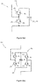
- Figure 6 shows in schematic form a third bypass protection circuit 100.
- the third bypass protection circuit 100 may replace one or more of both the first and second bypass protection circuits 50; 80 in any of the aforementioned first, second or third electrical assemblies 10; 60; 70 described hereinabove.
- the third bypass protection circuit 100 is similar to the second bypass protection circuit 80 and like features again share the same reference numerals.
- the third bypass protection circuit 100 does, however, differ from the second bypass protection circuit 80 in that it includes a second semiconductor protection element 82 in the form of a second semiconductor switch 102, and more particularly in the form of a second thyristor 104.
- the second semiconductor protection element 82 in the third bypass protection circuit 100 may instead be formed from a string of series-connected second thyristors 104.
- the second semiconductor protection element 82 in the third bypass protection circuit 100 is switchable between conducting and non-conducting conditions.
- the second semiconductor protection element 82 i.e. the second thyristor 104
- the second thyristor 104 blocks the flow of current therethrough in the forward direction F.
- the first current conducting path 56 of the third bypass protection circuit 100 again functions in the same manner as described hereinabove in relation to the first bypass protection circuit 50.
- the second current conducting path 84 provided by the second semiconductor protection element 82 i.e. the second thyristor 104, selectively diverts current flowing in the reverse direction through the corresponding switching assembly 26; 62; 72, e.g. a DC fault current, away from the said corresponding switching assembly 26; 62; 72.
- the second semiconductor protection element 82 i.e. the second thyristor 104, thereby again similarly helps to protect from damage the first switching elements 28 lying within a corresponding switching assembly 26; 62; 72.
- the first semiconductor protection element 52 is arranged in operative communication with a local control unit 110 that is programmed to switch the corresponding first semiconductor protection element 52 into its conducting condition.
- the local control unit may be programmed to switch the corresponding first semiconductor protection element 52 between its conducting and non-conducting conditions.
- the local control unit 110 is also arranged in operative communication with the second semiconductor protection element 82, i.e. the second semiconductor switch 102 in the form of the second thyristor 104, although this need not necessarily be the case.
- each local control unit 110 is shown in operative communication with a single corresponding first semiconductor protection element 52. In other embodiments of the invention, however, one or more local control units 110 may be arranged in operative communication with a plurality of corresponding first (and/or second) semiconductor protection elements 52.
- each local control unit 110 is arranged to draw power from an adjacent component within the corresponding electrical assembly 10; 60; 70.
- Figure 7 shows a third switching assembly 72 connected in parallel with which is a second bypass protection circuit 80.
- the third switching assembly 72 shown includes a power extraction circuit 112 that has a coil 114 which bisects the current path extending through the first chain-link sub-module 30 that defines the third switch assembly 72.
- An AC current flowing through the first chain-link sub-module 30 creates a magnetic flux which in turn generates a current in a conductor 116, e.g. a wire, that is wrapped around the coil 114.
- the conductor 116 is electrically connected with the local control unit 110 and so the generated current is able, via a rectifying means, to charge an energy storage device, e.g. a battery (not shown), on the local control unit 110.
- the battery is able subsequently to provide power to operate the said local control unit 110.
- a voltage appearing across the first chain-link sub-module 30 or across the capacitor 94 of an associated snubber circuit 92 may be used to charge the energy storage device within the local control unit 110.
- a resistor may be used to limit the current provided to the energy storage device.
- One or more of the local control units may, however, draw power in a different manner to the two techniques set out above.
- Such different manners of drawing power may include obtaining power from a nearby device, e.g. by way of a current loop or scavenging a voltage such as a capacitor voltage. It might also include ground powering with adequate electrical isolation, e.g. light triggered or laser power.
- each local control unit 110 is further programmed to act in accordance with an operating condition of a higher-level control unit (not shown) with which it is, in use, arranged in operative communication.
- the local control unit 110 may operate on its own if the higher-level control unit becomes de-energized or if the voltage across a particular chain-link sub-module 30; 44 becomes too high and is communicated as such by the higher-level control unit. In this latter regard the local control unit 110 is thereby able to provide a degree of overvoltage protection.
- the local control unit 110 may also be deactivated by the higher-level control unit if the higher-level control unit is operating normally and is fully energised.
- the local control unit 110 may be delay acting in order to allow the voltage across one or more chain-link sub-modules 30; 44 to rise to a minimum level, as set by the higher-level control unit.
- each local control unit 110 will each be placed in a standby mode.
- each local control unit 110 will be placed in an operational mode.
- a further consideration is that the power up time of each of the local control units 110 should be coordinated to allow the higher-level controller sufficient time to power up also.
Landscapes
- Engineering & Computer Science (AREA)
- Power Engineering (AREA)
- Inverter Devices (AREA)
- Power Conversion In General (AREA)
Claims (9)
- Ensemble électrique (60), destiné à être utilisé dans une partie de branche (12, 22) d'une branche de convertisseur (14) au sein d'un convertisseur de puissance CCHT (16), l'ensemble électrique (60) comprenant une pluralité d'ensembles de commutation (62), chaque ensemble de commutation (62) incluant une pluralité de sous-modules à maillon de chaîne (44) agencés pour définir un module à maillon de chaîne (42), chaque sous-module à maillon de chaîne (44) incluant au moins un commutateur à semi-conducteur (28) et au moins un dispositif de stockage d'énergie (38), le ou chaque commutateur à semi-conducteur (28) et le ou chaque dispositif de stockage d'énergie (38) de chaque sous-module à maillon de chaîne (44) se combinant pour fournir sélectivement une source de tension, chaque commutateur à semi-conducteur (28) pouvant être commuté de manière sélective entre des conditions conductrices et non conductrices, chaque commutateur à semi-conducteur (28) dans la condition conductrice permettant au courant de circuler à travers le commutateur à semi-conducteur (28) dans une première direction avant et de cette façon à travers ledit ensemble de commutation (62) dans la même direction avant, chaque ensemble de commutation (62) présentant un circuit de protection de dérivation (50) connecté en parallèle avec celui-ci, chaque circuit de protection de dérivation (50) incluant un premier élément de protection à semi-conducteur (52) pouvant être commuté sélectivement entre des conditions conductrices et non conductrices, le ou chaque dit premier élément de protection à semi-conducteur (52), alors dans la condition conductrice, fournissant un premier trajet conducteur de courant (56) dans la direction avant (F) pour détourner le courant circulant dans la direction avant (F) à travers l'ensemble de commutation (62) correspondant à distance dudit ensemble de commutation (62) correspondant.
- Ensemble électrique selon la revendication 1, dans lequel un ou plusieurs circuits de protection de dérivation (50, 80) inclut un second élément de protection à semi-conducteur (82) agencé pour fournir un second trajet conducteur de courant (56) dans une seconde direction inverse (R) opposée à la direction avant (F) pour détourner le courant circulant dans une direction inverse à travers l'ensemble de commutation (62) correspondant à distance dudit ensemble de commutation (62).
- Ensemble électrique selon la revendication 2, dans lequel le second élément de protection à semi-conducteur (82) d'un ou plusieurs circuits de protection de dérivation (80) est ou inclut un élément de vérification de courant passif (86) qui permet en continu au courant de circuler à travers celui-ci dans la direction inverse (R), tout en bloquant en continu la circulation de courant à travers celui-ci dans la direction avant (F).
- Ensemble électrique selon la revendication 2, dans lequel le second élément de protection à semi-conducteur (82) d'un ou plusieurs circuits de protection de dérivation (80) est ou inclut un commutateur à semi-conducteur (54, 104) pouvant être commuté sélectivement entre des conditions conductrices et non conductrices.
- Ensemble électrique selon l'une quelconque des revendications précédentes, dans lequel le premier élément de protection à semi-conducteur (52) d'un ou plusieurs circuits de protection de dérivation (50, 80) est connecté en série à un réacteur de limitation de courant (90).
- Ensemble électrique selon l'une quelconque des revendications précédentes, dans lequel le premier élément de protection à semi-conducteur (52) d'un ou plusieurs circuits de protection de dérivation (50, 80) est connecté en parallèle à un circuit d'amortissement (92).
- Ensemble électrique selon l'une quelconque des revendications précédentes, dans lequel le ou chaque premier élément de protection à semi-conducteur (52, 82) est agencé en communication fonctionnelle avec une unité de commande locale (110) programmée pour au moins commuter un dit premier élément de protection à semi-conducteur (52) dans sa condition conductrice.
- Ensemble électrique selon la revendication 7, dans lequel la ou chaque unité de commande locale (110) est agencée pour tirer de la puissance d'un composant adjacent dans l'ensemble électrique (60, 70).
- Ensemble électrique selon la revendication 7 ou la revendication 8, dans lequel la ou chaque unité de commande locale (110) est programmée en outre pour agir conformément à une condition fonctionnelle d'une unité de commande de plus haut niveau avec laquelle, lors d'une utilisation, elle est agencée en communication opérationnelle.
Priority Applications (1)
| Application Number | Priority Date | Filing Date | Title |
|---|---|---|---|
| EP15275062.6A EP3068008B1 (fr) | 2015-03-12 | 2015-03-12 | Améliorations apportées ou relatives à des convertisseurs de puissance à courant continu à haute tension |
Applications Claiming Priority (1)
| Application Number | Priority Date | Filing Date | Title |
|---|---|---|---|
| EP15275062.6A EP3068008B1 (fr) | 2015-03-12 | 2015-03-12 | Améliorations apportées ou relatives à des convertisseurs de puissance à courant continu à haute tension |
Publications (2)
| Publication Number | Publication Date |
|---|---|
| EP3068008A1 EP3068008A1 (fr) | 2016-09-14 |
| EP3068008B1 true EP3068008B1 (fr) | 2020-04-29 |
Family
ID=52672215
Family Applications (1)
| Application Number | Title | Priority Date | Filing Date |
|---|---|---|---|
| EP15275062.6A Active EP3068008B1 (fr) | 2015-03-12 | 2015-03-12 | Améliorations apportées ou relatives à des convertisseurs de puissance à courant continu à haute tension |
Country Status (1)
| Country | Link |
|---|---|
| EP (1) | EP3068008B1 (fr) |
Families Citing this family (7)
| Publication number | Priority date | Publication date | Assignee | Title |
|---|---|---|---|---|
| CN109874387B (zh) * | 2016-09-19 | 2020-05-15 | Abb瑞士股份有限公司 | 具有组织成集群的单元的模块化多电平变流器 |
| WO2018113926A1 (fr) * | 2016-12-20 | 2018-06-28 | Siemens Aktiengesellschaft | Convertisseur |
| WO2018184671A1 (fr) * | 2017-04-05 | 2018-10-11 | Siemens Aktiengesellschaft | Convertisseur multi-étagé polyphasé |
| SE543547C2 (en) | 2017-07-03 | 2021-03-23 | Abb Schweiz Ag | Submodule for a modular multilevel converter |
| EP3639354B1 (fr) * | 2017-08-09 | 2022-06-15 | Siemens Energy Global GmbH & Co. KG | Module de puissance pour un convertisseur de courant et convertisseur de courant à plusieurs niveaux |
| CN108258715B (zh) * | 2018-03-05 | 2022-01-14 | 南京南瑞继保电气有限公司 | 一种旁通晶闸管阀组巡检方法和控制装置 |
| WO2020228951A1 (fr) * | 2019-05-15 | 2020-11-19 | Siemens Aktiengesellschaft | Agencement avec un convertisseur à multiples niveaux |
Family Cites Families (4)
| Publication number | Priority date | Publication date | Assignee | Title |
|---|---|---|---|---|
| US5986909A (en) * | 1998-05-21 | 1999-11-16 | Robicon Corporation | Multiphase power supply with plural series connected cells and failed cell bypass |
| DE102005040543A1 (de) * | 2005-08-26 | 2007-03-01 | Siemens Ag | Stromrichterschaltung mit verteilten Energiespeichern |
| WO2013064310A1 (fr) * | 2011-11-03 | 2013-05-10 | Abb Technology Ag | Circuit convertisseur et procédé permettant de faire fonctionner un tel circuit convertisseur |
| EP2789091B1 (fr) * | 2011-12-05 | 2015-10-21 | ABB Technology AG | Procédé d'élimination d'un arc électrique généré par au moins une source de tension simple d'un circuit onduleur |
-
2015
- 2015-03-12 EP EP15275062.6A patent/EP3068008B1/fr active Active
Non-Patent Citations (1)
| Title |
|---|
| None * |
Also Published As
| Publication number | Publication date |
|---|---|
| EP3068008A1 (fr) | 2016-09-14 |
Similar Documents
| Publication | Publication Date | Title |
|---|---|---|
| EP3068008B1 (fr) | Améliorations apportées ou relatives à des convertisseurs de puissance à courant continu à haute tension | |
| EP2781013B1 (fr) | Module électronique de puissance | |
| US8687389B2 (en) | Apparatus having a converter | |
| EP3872944A1 (fr) | Dispositif de dissipation d'énergie à courant continu et son procédé de commande | |
| RU2683956C1 (ru) | Преобразовательное устройство и способ его защиты от короткого замыкания | |
| EP2747267B1 (fr) | Appareil électrique comprenant un convertisseur à cellules reliées en chaîne et un circuit de protection | |
| KR20120089359A (ko) | 고전압용 컨버터 | |
| CN211930497U (zh) | 变换器模块和电压中间电路变换器 | |
| KR20190121829A (ko) | 전류 경로를 분리하기 위한 스위칭 디바이스 | |
| US9847642B2 (en) | Control circuit | |
| WO2016037854A1 (fr) | Convertisseur de source de tension | |
| US20180115253A1 (en) | Improvements in or relating to electrical assemblies | |
| EP2849306A1 (fr) | Convertisseur de source de tension | |
| EP3544141A1 (fr) | Agencement électrique | |
| KR101558862B1 (ko) | 모듈러 멀티 레벨 컨버터 및 이를 포함하는 dc 사고 전류 저감 장치 | |
| EP3338336B1 (fr) | Ensemble électrique | |
| CN218868124U (zh) | 具有支撑结构的功率转换器装置 | |
| WO2020038704A1 (fr) | Valve de commutation | |
| EP3534523B1 (fr) | Améliorations apportées ou se rapportant à des convertisseurs de puissance à courant continu à haute tension | |
| CN112868179A (zh) | 电子阀装置 | |
| CN115004531A (zh) | 电气组合件 |
Legal Events
| Date | Code | Title | Description |
|---|---|---|---|
| PUAI | Public reference made under article 153(3) epc to a published international application that has entered the european phase |
Free format text: ORIGINAL CODE: 0009012 |
|
| AK | Designated contracting states |
Kind code of ref document: A1 Designated state(s): AL AT BE BG CH CY CZ DE DK EE ES FI FR GB GR HR HU IE IS IT LI LT LU LV MC MK MT NL NO PL PT RO RS SE SI SK SM TR |
|
| AX | Request for extension of the european patent |
Extension state: BA ME |
|
| STAA | Information on the status of an ep patent application or granted ep patent |
Free format text: STATUS: REQUEST FOR EXAMINATION WAS MADE |
|
| 17P | Request for examination filed |
Effective date: 20170314 |
|
| RBV | Designated contracting states (corrected) |
Designated state(s): AL AT BE BG CH CY CZ DE DK EE ES FI FR GB GR HR HU IE IS IT LI LT LU LV MC MK MT NL NO PL PT RO RS SE SI SK SM TR |
|
| GRAP | Despatch of communication of intention to grant a patent |
Free format text: ORIGINAL CODE: EPIDOSNIGR1 |
|
| STAA | Information on the status of an ep patent application or granted ep patent |
Free format text: STATUS: GRANT OF PATENT IS INTENDED |
|
| INTG | Intention to grant announced |
Effective date: 20191219 |
|
| RIN1 | Information on inventor provided before grant (corrected) |
Inventor name: CHIVITE-ZABALZA, FRANCISCO JAVIER Inventor name: MORENO MUNOZ, FRANCISCO JOSE Inventor name: OATES, COLIN DONALD MURRAY Inventor name: GREGOIRE, JEROME |
|
| GRAS | Grant fee paid |
Free format text: ORIGINAL CODE: EPIDOSNIGR3 |
|
| GRAA | (expected) grant |
Free format text: ORIGINAL CODE: 0009210 |
|
| STAA | Information on the status of an ep patent application or granted ep patent |
Free format text: STATUS: THE PATENT HAS BEEN GRANTED |
|
| AK | Designated contracting states |
Kind code of ref document: B1 Designated state(s): AL AT BE BG CH CY CZ DE DK EE ES FI FR GB GR HR HU IE IS IT LI LT LU LV MC MK MT NL NO PL PT RO RS SE SI SK SM TR |
|
| REG | Reference to a national code |
Ref country code: GB Ref legal event code: FG4D |
|
| REG | Reference to a national code |
Ref country code: CH Ref legal event code: EP |
|
| REG | Reference to a national code |
Ref country code: AT Ref legal event code: REF Ref document number: 1264744 Country of ref document: AT Kind code of ref document: T Effective date: 20200515 |
|
| REG | Reference to a national code |
Ref country code: DE Ref legal event code: R096 Ref document number: 602015051543 Country of ref document: DE |
|
| REG | Reference to a national code |
Ref country code: IE Ref legal event code: FG4D |
|
| REG | Reference to a national code |
Ref country code: SE Ref legal event code: TRGR |
|
| REG | Reference to a national code |
Ref country code: NL Ref legal event code: MP Effective date: 20200429 |
|
| REG | Reference to a national code |
Ref country code: LT Ref legal event code: MG4D |
|
| PG25 | Lapsed in a contracting state [announced via postgrant information from national office to epo] |
Ref country code: FI Free format text: LAPSE BECAUSE OF FAILURE TO SUBMIT A TRANSLATION OF THE DESCRIPTION OR TO PAY THE FEE WITHIN THE PRESCRIBED TIME-LIMIT Effective date: 20200429 Ref country code: LT Free format text: LAPSE BECAUSE OF FAILURE TO SUBMIT A TRANSLATION OF THE DESCRIPTION OR TO PAY THE FEE WITHIN THE PRESCRIBED TIME-LIMIT Effective date: 20200429 Ref country code: GR Free format text: LAPSE BECAUSE OF FAILURE TO SUBMIT A TRANSLATION OF THE DESCRIPTION OR TO PAY THE FEE WITHIN THE PRESCRIBED TIME-LIMIT Effective date: 20200730 Ref country code: NO Free format text: LAPSE BECAUSE OF FAILURE TO SUBMIT A TRANSLATION OF THE DESCRIPTION OR TO PAY THE FEE WITHIN THE PRESCRIBED TIME-LIMIT Effective date: 20200729 Ref country code: PT Free format text: LAPSE BECAUSE OF FAILURE TO SUBMIT A TRANSLATION OF THE DESCRIPTION OR TO PAY THE FEE WITHIN THE PRESCRIBED TIME-LIMIT Effective date: 20200831 Ref country code: IS Free format text: LAPSE BECAUSE OF FAILURE TO SUBMIT A TRANSLATION OF THE DESCRIPTION OR TO PAY THE FEE WITHIN THE PRESCRIBED TIME-LIMIT Effective date: 20200829 |
|
| REG | Reference to a national code |
Ref country code: AT Ref legal event code: MK05 Ref document number: 1264744 Country of ref document: AT Kind code of ref document: T Effective date: 20200429 |
|
| PG25 | Lapsed in a contracting state [announced via postgrant information from national office to epo] |
Ref country code: BG Free format text: LAPSE BECAUSE OF FAILURE TO SUBMIT A TRANSLATION OF THE DESCRIPTION OR TO PAY THE FEE WITHIN THE PRESCRIBED TIME-LIMIT Effective date: 20200729 Ref country code: HR Free format text: LAPSE BECAUSE OF FAILURE TO SUBMIT A TRANSLATION OF THE DESCRIPTION OR TO PAY THE FEE WITHIN THE PRESCRIBED TIME-LIMIT Effective date: 20200429 Ref country code: RS Free format text: LAPSE BECAUSE OF FAILURE TO SUBMIT A TRANSLATION OF THE DESCRIPTION OR TO PAY THE FEE WITHIN THE PRESCRIBED TIME-LIMIT Effective date: 20200429 Ref country code: LV Free format text: LAPSE BECAUSE OF FAILURE TO SUBMIT A TRANSLATION OF THE DESCRIPTION OR TO PAY THE FEE WITHIN THE PRESCRIBED TIME-LIMIT Effective date: 20200429 |
|
| PG25 | Lapsed in a contracting state [announced via postgrant information from national office to epo] |
Ref country code: AL Free format text: LAPSE BECAUSE OF FAILURE TO SUBMIT A TRANSLATION OF THE DESCRIPTION OR TO PAY THE FEE WITHIN THE PRESCRIBED TIME-LIMIT Effective date: 20200429 Ref country code: NL Free format text: LAPSE BECAUSE OF FAILURE TO SUBMIT A TRANSLATION OF THE DESCRIPTION OR TO PAY THE FEE WITHIN THE PRESCRIBED TIME-LIMIT Effective date: 20200429 |
|
| PG25 | Lapsed in a contracting state [announced via postgrant information from national office to epo] |
Ref country code: ES Free format text: LAPSE BECAUSE OF FAILURE TO SUBMIT A TRANSLATION OF THE DESCRIPTION OR TO PAY THE FEE WITHIN THE PRESCRIBED TIME-LIMIT Effective date: 20200429 Ref country code: DK Free format text: LAPSE BECAUSE OF FAILURE TO SUBMIT A TRANSLATION OF THE DESCRIPTION OR TO PAY THE FEE WITHIN THE PRESCRIBED TIME-LIMIT Effective date: 20200429 Ref country code: AT Free format text: LAPSE BECAUSE OF FAILURE TO SUBMIT A TRANSLATION OF THE DESCRIPTION OR TO PAY THE FEE WITHIN THE PRESCRIBED TIME-LIMIT Effective date: 20200429 Ref country code: EE Free format text: LAPSE BECAUSE OF FAILURE TO SUBMIT A TRANSLATION OF THE DESCRIPTION OR TO PAY THE FEE WITHIN THE PRESCRIBED TIME-LIMIT Effective date: 20200429 Ref country code: CZ Free format text: LAPSE BECAUSE OF FAILURE TO SUBMIT A TRANSLATION OF THE DESCRIPTION OR TO PAY THE FEE WITHIN THE PRESCRIBED TIME-LIMIT Effective date: 20200429 Ref country code: RO Free format text: LAPSE BECAUSE OF FAILURE TO SUBMIT A TRANSLATION OF THE DESCRIPTION OR TO PAY THE FEE WITHIN THE PRESCRIBED TIME-LIMIT Effective date: 20200429 Ref country code: IT Free format text: LAPSE BECAUSE OF FAILURE TO SUBMIT A TRANSLATION OF THE DESCRIPTION OR TO PAY THE FEE WITHIN THE PRESCRIBED TIME-LIMIT Effective date: 20200429 Ref country code: SM Free format text: LAPSE BECAUSE OF FAILURE TO SUBMIT A TRANSLATION OF THE DESCRIPTION OR TO PAY THE FEE WITHIN THE PRESCRIBED TIME-LIMIT Effective date: 20200429 |
|
| REG | Reference to a national code |
Ref country code: DE Ref legal event code: R097 Ref document number: 602015051543 Country of ref document: DE |
|
| PG25 | Lapsed in a contracting state [announced via postgrant information from national office to epo] |
Ref country code: SK Free format text: LAPSE BECAUSE OF FAILURE TO SUBMIT A TRANSLATION OF THE DESCRIPTION OR TO PAY THE FEE WITHIN THE PRESCRIBED TIME-LIMIT Effective date: 20200429 Ref country code: PL Free format text: LAPSE BECAUSE OF FAILURE TO SUBMIT A TRANSLATION OF THE DESCRIPTION OR TO PAY THE FEE WITHIN THE PRESCRIBED TIME-LIMIT Effective date: 20200429 |
|
| PLBE | No opposition filed within time limit |
Free format text: ORIGINAL CODE: 0009261 |
|
| STAA | Information on the status of an ep patent application or granted ep patent |
Free format text: STATUS: NO OPPOSITION FILED WITHIN TIME LIMIT |
|
| 26N | No opposition filed |
Effective date: 20210201 |
|
| PG25 | Lapsed in a contracting state [announced via postgrant information from national office to epo] |
Ref country code: SI Free format text: LAPSE BECAUSE OF FAILURE TO SUBMIT A TRANSLATION OF THE DESCRIPTION OR TO PAY THE FEE WITHIN THE PRESCRIBED TIME-LIMIT Effective date: 20200429 |
|
| PG25 | Lapsed in a contracting state [announced via postgrant information from national office to epo] |
Ref country code: MC Free format text: LAPSE BECAUSE OF FAILURE TO SUBMIT A TRANSLATION OF THE DESCRIPTION OR TO PAY THE FEE WITHIN THE PRESCRIBED TIME-LIMIT Effective date: 20200429 |
|
| REG | Reference to a national code |
Ref country code: CH Ref legal event code: PL |
|
| REG | Reference to a national code |
Ref country code: BE Ref legal event code: MM Effective date: 20210331 |
|
| PG25 | Lapsed in a contracting state [announced via postgrant information from national office to epo] |
Ref country code: IE Free format text: LAPSE BECAUSE OF NON-PAYMENT OF DUE FEES Effective date: 20210312 Ref country code: LI Free format text: LAPSE BECAUSE OF NON-PAYMENT OF DUE FEES Effective date: 20210331 Ref country code: LU Free format text: LAPSE BECAUSE OF NON-PAYMENT OF DUE FEES Effective date: 20210312 Ref country code: CH Free format text: LAPSE BECAUSE OF NON-PAYMENT OF DUE FEES Effective date: 20210331 |
|
| PG25 | Lapsed in a contracting state [announced via postgrant information from national office to epo] |
Ref country code: BE Free format text: LAPSE BECAUSE OF NON-PAYMENT OF DUE FEES Effective date: 20210331 |
|
| PG25 | Lapsed in a contracting state [announced via postgrant information from national office to epo] |
Ref country code: HU Free format text: LAPSE BECAUSE OF FAILURE TO SUBMIT A TRANSLATION OF THE DESCRIPTION OR TO PAY THE FEE WITHIN THE PRESCRIBED TIME-LIMIT; INVALID AB INITIO Effective date: 20150312 |
|
| P01 | Opt-out of the competence of the unified patent court (upc) registered |
Effective date: 20230522 |
|
| PG25 | Lapsed in a contracting state [announced via postgrant information from national office to epo] |
Ref country code: CY Free format text: LAPSE BECAUSE OF FAILURE TO SUBMIT A TRANSLATION OF THE DESCRIPTION OR TO PAY THE FEE WITHIN THE PRESCRIBED TIME-LIMIT Effective date: 20200429 |
|
| PG25 | Lapsed in a contracting state [announced via postgrant information from national office to epo] |
Ref country code: MK Free format text: LAPSE BECAUSE OF FAILURE TO SUBMIT A TRANSLATION OF THE DESCRIPTION OR TO PAY THE FEE WITHIN THE PRESCRIBED TIME-LIMIT Effective date: 20200429 |
|
| PGFP | Annual fee paid to national office [announced via postgrant information from national office to epo] |
Ref country code: DE Payment date: 20240220 Year of fee payment: 10 Ref country code: GB Payment date: 20240221 Year of fee payment: 10 |
|
| PGFP | Annual fee paid to national office [announced via postgrant information from national office to epo] |
Ref country code: SE Payment date: 20240220 Year of fee payment: 10 Ref country code: FR Payment date: 20240220 Year of fee payment: 10 |