EP3066899B1 - Flexible circuit board for led lighting fixtures - Google Patents
Flexible circuit board for led lighting fixtures Download PDFInfo
- Publication number
- EP3066899B1 EP3066899B1 EP14802554.7A EP14802554A EP3066899B1 EP 3066899 B1 EP3066899 B1 EP 3066899B1 EP 14802554 A EP14802554 A EP 14802554A EP 3066899 B1 EP3066899 B1 EP 3066899B1
- Authority
- EP
- European Patent Office
- Prior art keywords
- metallic
- led packages
- laminate sheet
- perforations
- exposed
- Prior art date
- Legal status (The legal status is an assumption and is not a legal conclusion. Google has not performed a legal analysis and makes no representation as to the accuracy of the status listed.)
- Active
Links
Images


Classifications
-
- H—ELECTRICITY
- H05—ELECTRIC TECHNIQUES NOT OTHERWISE PROVIDED FOR
- H05K—PRINTED CIRCUITS; CASINGS OR CONSTRUCTIONAL DETAILS OF ELECTRIC APPARATUS; MANUFACTURE OF ASSEMBLAGES OF ELECTRICAL COMPONENTS
- H05K1/00—Printed circuits
- H05K1/18—Printed circuits structurally associated with non-printed electric components
- H05K1/189—Printed circuits structurally associated with non-printed electric components characterised by the use of flexible or folded printed circuits
-
- H—ELECTRICITY
- H10—SEMICONDUCTOR DEVICES; ELECTRIC SOLID-STATE DEVICES NOT OTHERWISE PROVIDED FOR
- H10W—GENERIC PACKAGES, INTERCONNECTIONS, CONNECTORS OR OTHER CONSTRUCTIONAL DETAILS OF DEVICES COVERED BY CLASS H10
- H10W90/00—Package configurations
-
- H—ELECTRICITY
- H05—ELECTRIC TECHNIQUES NOT OTHERWISE PROVIDED FOR
- H05K—PRINTED CIRCUITS; CASINGS OR CONSTRUCTIONAL DETAILS OF ELECTRIC APPARATUS; MANUFACTURE OF ASSEMBLAGES OF ELECTRICAL COMPONENTS
- H05K3/00—Apparatus or processes for manufacturing printed circuits
- H05K3/10—Apparatus or processes for manufacturing printed circuits in which conductive material is applied to the insulating support in such a manner as to form the desired conductive pattern
- H05K3/103—Apparatus or processes for manufacturing printed circuits in which conductive material is applied to the insulating support in such a manner as to form the desired conductive pattern by bonding or embedding conductive wires or strips
-
- H—ELECTRICITY
- H10—SEMICONDUCTOR DEVICES; ELECTRIC SOLID-STATE DEVICES NOT OTHERWISE PROVIDED FOR
- H10H—INORGANIC LIGHT-EMITTING SEMICONDUCTOR DEVICES HAVING POTENTIAL BARRIERS
- H10H20/00—Individual inorganic light-emitting semiconductor devices having potential barriers, e.g. light-emitting diodes [LED]
- H10H20/80—Constructional details
- H10H20/85—Packages
- H10H20/855—Optical field-shaping means, e.g. lenses
- H10H20/856—Reflecting means
-
- H—ELECTRICITY
- H10—SEMICONDUCTOR DEVICES; ELECTRIC SOLID-STATE DEVICES NOT OTHERWISE PROVIDED FOR
- H10H—INORGANIC LIGHT-EMITTING SEMICONDUCTOR DEVICES HAVING POTENTIAL BARRIERS
- H10H20/00—Individual inorganic light-emitting semiconductor devices having potential barriers, e.g. light-emitting diodes [LED]
- H10H20/80—Constructional details
- H10H20/85—Packages
- H10H20/857—Interconnections, e.g. lead-frames, bond wires or solder balls
-
- H—ELECTRICITY
- H05—ELECTRIC TECHNIQUES NOT OTHERWISE PROVIDED FOR
- H05K—PRINTED CIRCUITS; CASINGS OR CONSTRUCTIONAL DETAILS OF ELECTRIC APPARATUS; MANUFACTURE OF ASSEMBLAGES OF ELECTRICAL COMPONENTS
- H05K1/00—Printed circuits
- H05K1/02—Details
- H05K1/0274—Optical details, e.g. printed circuits comprising integral optical means
-
- H—ELECTRICITY
- H05—ELECTRIC TECHNIQUES NOT OTHERWISE PROVIDED FOR
- H05K—PRINTED CIRCUITS; CASINGS OR CONSTRUCTIONAL DETAILS OF ELECTRIC APPARATUS; MANUFACTURE OF ASSEMBLAGES OF ELECTRICAL COMPONENTS
- H05K1/00—Printed circuits
- H05K1/02—Details
- H05K1/0286—Programmable, customizable or modifiable circuits
- H05K1/0287—Programmable, customizable or modifiable circuits having an universal lay-out, e.g. pad or land grid patterns or mesh patterns
-
- H—ELECTRICITY
- H05—ELECTRIC TECHNIQUES NOT OTHERWISE PROVIDED FOR
- H05K—PRINTED CIRCUITS; CASINGS OR CONSTRUCTIONAL DETAILS OF ELECTRIC APPARATUS; MANUFACTURE OF ASSEMBLAGES OF ELECTRICAL COMPONENTS
- H05K1/00—Printed circuits
- H05K1/18—Printed circuits structurally associated with non-printed electric components
- H05K1/181—Printed circuits structurally associated with non-printed electric components associated with surface mounted components
-
- H—ELECTRICITY
- H05—ELECTRIC TECHNIQUES NOT OTHERWISE PROVIDED FOR
- H05K—PRINTED CIRCUITS; CASINGS OR CONSTRUCTIONAL DETAILS OF ELECTRIC APPARATUS; MANUFACTURE OF ASSEMBLAGES OF ELECTRICAL COMPONENTS
- H05K2201/00—Indexing scheme relating to printed circuits covered by H05K1/00
- H05K2201/10—Details of components or other objects attached to or integrated in a printed circuit board
- H05K2201/10007—Types of components
- H05K2201/10106—Light emitting diode [LED]
-
- H—ELECTRICITY
- H05—ELECTRIC TECHNIQUES NOT OTHERWISE PROVIDED FOR
- H05K—PRINTED CIRCUITS; CASINGS OR CONSTRUCTIONAL DETAILS OF ELECTRIC APPARATUS; MANUFACTURE OF ASSEMBLAGES OF ELECTRICAL COMPONENTS
- H05K2201/00—Indexing scheme relating to printed circuits covered by H05K1/00
- H05K2201/10—Details of components or other objects attached to or integrated in a printed circuit board
- H05K2201/10227—Other objects, e.g. metallic pieces
- H05K2201/1028—Thin metal strips as connectors or conductors
-
- H—ELECTRICITY
- H05—ELECTRIC TECHNIQUES NOT OTHERWISE PROVIDED FOR
- H05K—PRINTED CIRCUITS; CASINGS OR CONSTRUCTIONAL DETAILS OF ELECTRIC APPARATUS; MANUFACTURE OF ASSEMBLAGES OF ELECTRICAL COMPONENTS
- H05K2201/00—Indexing scheme relating to printed circuits covered by H05K1/00
- H05K2201/20—Details of printed circuits not provided for in H05K2201/01 - H05K2201/10
- H05K2201/2054—Light-reflecting surface, e.g. conductors, substrates, coatings, dielectrics
-
- H—ELECTRICITY
- H05—ELECTRIC TECHNIQUES NOT OTHERWISE PROVIDED FOR
- H05K—PRINTED CIRCUITS; CASINGS OR CONSTRUCTIONAL DETAILS OF ELECTRIC APPARATUS; MANUFACTURE OF ASSEMBLAGES OF ELECTRICAL COMPONENTS
- H05K2203/00—Indexing scheme relating to apparatus or processes for manufacturing printed circuits covered by H05K3/00
- H05K2203/06—Lamination
- H05K2203/063—Lamination of preperforated insulating layer
-
- H—ELECTRICITY
- H10—SEMICONDUCTOR DEVICES; ELECTRIC SOLID-STATE DEVICES NOT OTHERWISE PROVIDED FOR
- H10H—INORGANIC LIGHT-EMITTING SEMICONDUCTOR DEVICES HAVING POTENTIAL BARRIERS
- H10H20/00—Individual inorganic light-emitting semiconductor devices having potential barriers, e.g. light-emitting diodes [LED]
- H10H20/01—Manufacture or treatment
- H10H20/032—Manufacture or treatment of electrodes
-
- H—ELECTRICITY
- H10—SEMICONDUCTOR DEVICES; ELECTRIC SOLID-STATE DEVICES NOT OTHERWISE PROVIDED FOR
- H10H—INORGANIC LIGHT-EMITTING SEMICONDUCTOR DEVICES HAVING POTENTIAL BARRIERS
- H10H20/00—Individual inorganic light-emitting semiconductor devices having potential barriers, e.g. light-emitting diodes [LED]
- H10H20/01—Manufacture or treatment
- H10H20/036—Manufacture or treatment of packages
-
- H—ELECTRICITY
- H10—SEMICONDUCTOR DEVICES; ELECTRIC SOLID-STATE DEVICES NOT OTHERWISE PROVIDED FOR
- H10H—INORGANIC LIGHT-EMITTING SEMICONDUCTOR DEVICES HAVING POTENTIAL BARRIERS
- H10H20/00—Individual inorganic light-emitting semiconductor devices having potential barriers, e.g. light-emitting diodes [LED]
- H10H20/01—Manufacture or treatment
- H10H20/036—Manufacture or treatment of packages
- H10H20/0363—Manufacture or treatment of packages of optical field-shaping means
-
- H—ELECTRICITY
- H10—SEMICONDUCTOR DEVICES; ELECTRIC SOLID-STATE DEVICES NOT OTHERWISE PROVIDED FOR
- H10H—INORGANIC LIGHT-EMITTING SEMICONDUCTOR DEVICES HAVING POTENTIAL BARRIERS
- H10H20/00—Individual inorganic light-emitting semiconductor devices having potential barriers, e.g. light-emitting diodes [LED]
- H10H20/01—Manufacture or treatment
- H10H20/036—Manufacture or treatment of packages
- H10H20/0364—Manufacture or treatment of packages of interconnections
Definitions
- This disclosure relates to circuit fabrication, and more specifically to flexible circuit board fabrication and circuits produced therefrom.
- SMD surface mount devices
- the circuit board may be a flexible circuit board.
- Effectively attaching SMDs to flexible circuit boards involves a number of non-trivial challenges. Examples thereof are illustrated in DE 10 2010 049 333 A1 ; EP 0 677 695 A1 ; US 7,446,347 B2 ; EP 1 473 978 A1 and US 2008/295327 A1 .
- Publication DE 10 2010 049 333 A1 relates to an endless band shaped structure for mounting power LEDs.
- the structure comprises a double sided adhesive band with a flexible solderable conductive strip structure applied on one side of the band shaped structure.
- the conductive strip structure is covered with a reflecting film, wherein the reflecting film is punched in areas for mounting power LEDs.
- a flexible circuit includes a perforated upper laminate sheet including a plurality of perforations; a lower laminate sheet; a plurality of metallic conductors laminated between the perforated upper laminate sheet and the lower laminate sheet, wherein the metallic conductors are arranged side by side and extend in a longitudinal direction between the upper and lower laminate sheet, wherein each of the metallic conductors is a metallic ribbon, a metallic tape or a metallic wire and wherein each of the metallic conductors has a plurality of sets of two metallic contacts, wherein the two metallic contacts of each set are on two separate portions of the same metallic conductor, the separate portions formed by perforations in the metallic conductor, wherein each set is exposed by a respective one of the perforations; and a plurality of surface mount devices, wherein each of the surface mount devices is attached to a respective one of the sets of two metallic contacts.
- a method of fabricating a flexible circuit includes a perforating of an upper laminate sheet to form a plurality of perforations in the upper laminate sheet; a laminating of a plurality of metallic conductors between the perforated upper laminate sheet and a lower laminate sheet, wherein each of the metallic conductors is a metallic ribbon, a metallic tape or a metallic wire and wherein each of the metallic conductors has a plurality of portions each exposed by a respective one of the perforations; a perforating of each of the exposed portions of the metallic conductors to respectively form sets of two metallic contacts in each of the exposed portions of the metallic conductors; and an attaching of a LED package respectively to each set of two metallic contacts.
- a method of fabricating a flexible circuit includes a providing of a plurality of plastic housings including a plurality of perforations, wherein each of the plastic housings includes a perforation; a molding of the plurality of plastic housings along a metallic conductor, so that each of a plurality of portions of the metallic conductor is exposed by a respective one of the perforations of the plastic housings, wherein the metallic conductor is a metallic ribbon, a metallic tape or a metallic wire; a perforating of the metallic conductor in each of the exposed portions to form a set of two metallic contacts in each of the exposed portions, wherein each set is exposed by a respective one of the perforations of the plastic housings; a forming of a string of LED packages by attaching a LED package respectively to each set of two metallic contacts; and a laminating of the string of LED packages between a lower laminate sheet and a perforated upper laminate sheet, wherein each of the perforations in the upper laminate sheet exposes a respective one of
- LED packages are attached to multiple metal conductors that are laminated between two laminate sheets, forming a flexible LED circuit.
- the LED packages may be attached prior to laminating the conductive metal strips or after the strips are laminated within the flexible circuit board.
- the metal strips may be perforated using a hole punching mechanism, precision blades, or some other metal-cutting technique for the placement of LED package leads.
- the LED packages may be attached to the conductive strips using solder or a conductive epoxy and the upper laminate layer may include perforations exposing portions of the metal strips for the attachment of the LED packages.
- Strings of LED packages may be fabricated, in some embodiments, by attaching LED packages to conductive strips and these strings may be laminated between flexible sheets to form a laminated LED circuit.
- Plastic housings may aid in attaching the LED packages to the conductive strips, and these housings may help hold the strips together when they are perforated prior to attaching the LED packages.
- the plastic housings and/or the laminate sheets may be made of a reflective material.
- flexible substrates with screen printed circuit patterns are used to fabricate flexible circuits.
- the circuits may be printed using a silver ink, or other conductive ink.
- conductive epoxies used to attach the SMDs to the printed circuit may fail due to adhesions problems with the substrate which is typically polyester (PET). More specifically, the joint holding, for example, a 5 mm x 3 mm LED package may fail because before the conductive epoxy is cured, the epoxy may cause the silver trace of the printed circuit to remove from the PET substrate.
- a light engine that uses a laminated circuit structure may be manufactured using the techniques described herein.
- the metallic conductor may be, for example, gold, aluminum, silver, copper, or any other suitable conductive material.
- a light engine uses a flexible laminated circuit structure to assemble an LED array for area lighting fixtures. The spacing of the LEDs within the LED circuit could be determined, for example, by the spacing of the final application.
- the LED packages might be spaced every inch producing a 12 x 12 array about one square foot for an overhead area light module, in one example.
- the LED packages in each strip would be in series, and the driver would be designed to accommodate that voltage, with each strip in parallel to one another, in some embodiments.
- a plastic housing may be molded directly onto a copper ribbon and LED packages may be attached within the housing.
- the plastic housing is molded from a reflective polymer.
- the spacing of the housings along the length of the copper ribbon would be determined by the layout of the light engine in the luminaire, in some embodiments.
- twelve plastic housings may be molded onto twelve one-foot sections of copper ribbon.
- the copper ribbon within the housings is perforated and LED packages may be attached making twelve strings of LED packages. These twelve strings of LED packages may then be laminated within a roll of PET, producing a 12 x 12 array about one square foot for an overhead area light module, in one example.
- Other lengths and numbers of LED packages are possible, and the length may be chosen based on the desired DC voltage that the lighting driver will apply across the string, in some embodiments.
- the techniques disclosed may be used to laminate various circuit grids within flexible laminate sheets, as well as for the attachment of any SMD onto a flexible laminated circuit.
- examples are provided for fabricating a flexible LED lighting circuit with strings of LED packages.
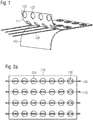
- Figure 1 shows four copper ribbons being laminated between two sheets, according to an embodiment of the present invention.
- the upper laminate sheet includes perforations placed for the eventual location of LED packages on the copper ribbon.
- the perforations in this example are circular; however, they may be oval, rectangular, or any other suitable shape, in other embodiments.
- the upper laminate sheet is a transparent plastic such as polyethylene terephthalate (PET), or other suitable polymer, while the lower laminate sheet has a reflective upper surface. In other embodiments, the upper laminate sheet may have a reflective upper surface.
- PET polyethylene terephthalate
- the thin copper ribbon may be around .003 inches thick.
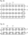
- Figure 2a shows an example flexible laminated circuit board with perforations in the copper ribbons, according to one embodiment of the present invention.
- the laminated sheet includes four copper ribbons and the upper laminate sheet has multiple perforations exposing portions of the copper ribbons for the eventual placement of LED packages.
- the upper laminate sheet in this particular embodiment is transparent and the entire copper ribbons are visible.
- each of the four copper ribbons has been perforated for the eventual placement of the anode and cathode leads of the LED packages.
- the perforation is made using a hole-punching mechanism; however, precision blades or other techniques may be used to sever the copper ribbons.
- Figure 2b shows an example flexible laminated circuit board with perforations in the copper ribbons and a number of LED packages placed across the perforations, according to one embodiment of the present invention.
- the laminated sheet in this example embodiment includes four copper ribbons and the upper laminate sheet has multiple perforations exposing portions of the copper ribbons for the eventual placement of LED packages.
- the upper laminate sheet in this particular embodiment is transparent and the entire copper ribbons are visible.
- an LED package has been placed across a perforation of each of the four copper ribbons.
- the LED packages may be attached using a conductive epoxy or solder, in some embodiments.
- Figure 2c shows another example flexible laminated LED circuit board wherein the series string of LED packages has LED packages connected sideways, or in a serpentine configuration, according to an embodiment of the present invention.
- the flexible laminated LED circuit board includes only two series strings of LED packages, and the sideways connection of the LED packages helps to minimize the stresses on the connections if the substrate is bent. In one such example, the sideways connection relaxes the tolerance on the length of the conductive strip decreasing any shorting worries.
- Figure 3 illustrates an example flexible laminated LED circuit including two LED strings connected in parallel, according to an embodiment of the present invention.
- two strings of LED packages have been connected in series along conductive wires to form a flexible LED circuit.
- This particular example illustrates the flexibility of such a laminated LED circuit.
- Figures 4a-d collectively illustrate the formation of a flexible laminated circuit board, according to an example which is not part of the present invention.
- Figure 4a shows an example of a lower laminate sheet with four columns of conductive strips. The conductive strips are spaced such that LED packages may be attached at the spaces between strips, thus forming four LED strings. The conductive strips could be, for example, sections of copper ribbon, wires, or any other conductive material suitable for depositing LED packages.
- Figure 4b shows an example upper laminate sheet with multiple perforations matching the location of the spaces between the conductive strips.
- Figure 4c shows an example of a laminated circuit board after the lower laminate sheet of Figure 4a and the upper laminate sheet of Figure 4b are laminated together.
- the upper laminate sheet is not transparent, such that the conductive strips are only visible at the perforations.
- the perforations expose the spaces between the conductive strips, and an LED circuit package may be soldered or otherwise attached across these spaces.
- Figure 4d shows an example of a laminated circuit board after LED packages have been attached across the spaces between the conductive strips.
- Figures 5a-c collectively illustrate the formation of a string of LED packages surrounded by plastic housings, according to one embodiment of the present invention.
- Figures 5a and 5c show various cross-sectional views of the formation of the plastic housing and attachment of an LED package
- figure 5b shows a view from above of the formation of the plastic housing and attachment of an LED package, according to an embodiment of the present invention.
- a length of copper ribbon is dispensed from a roll.
- a housing mold forms a plastic housing around the copper ribbon and a perforator cuts the copper ribbon.
- the plastic housing is made from a reflective polymer.
- the housings may have a hole in the center and may resemble a ring when completed, in some embodiments.
- the perforator could be a hole-punching mechanism similar to the one shown, one or more precision blades, or any other device for cutting the copper ribbon and providing two pads for the placement of the anode and cathode leads of the LED packages.
- solder or epoxy may be dispensed on the exposed ends of the copper ribbon within the plastic housing and an LED package may be deposited onto the copper ribbon.
- an epoxy curer may cure the epoxy in order to fully attach the LED package.
- Figure 6 shows a string of LED packages attached to a copper ribbon within plastic housings, according to one embodiment of the present invention.
- many LED packages may be fabricated in a single long string, and the string can be cut to any desired length or number of LED packages.
- the desired length and number of LED packages in each string may be dependent on the desired DC voltage that the lighting driver would apply across the string, in some embodiments.
- the string is cut to a string of five LED packages for the eventual placement within a flexible laminated circuit board. Once the strips are cut to length, they may be attached or laminated to a piece of flexible material (e.g., PET), in some embodiments.
- the plastic housing is reflective and little photometric performance is lost if the flexible substrate is clear.
- Figure 7 shows four strings of LED packages on copper ribbons being laminated between two laminate sheets, according to an embodiment of the present invention.
- the upper laminate sheet includes perforations so that the upper laminate sheet does not cover the LED packages on the copper ribbons.
- the perforations in this example are circular; however, they may be oval, rectangular, or any other suitable shape, in other embodiments.
- the upper laminate sheet is a transparent plastic such as polyethylene terephthalate (PET), or other suitable polymer, while the lower laminate sheet has a reflective upper surface.
- PET polyethylene terephthalate
- the upper laminate sheet may have a reflective upper surface.
- this particular example shows four strings of LED packages laminated between two sheets, other embodiments may include fewer or more strings of LED packages and the copper ribbons may be replaced with copper wires, or any other suitable conductive material.
- Figure 8 illustrates a method for fabricating a flexible laminated LED circuit, according to an embodiment of the present invention.
- the method may begin with providing 801 at least one conductive wire.
- the conductive wire may be a copper ribbon, copper wire, or copper tape.
- the method may continue with determining 802, whether a plastic housing will be formed around the conductive wire for the placement of the LED packages. If a plastic housing will be formed for the LED packages, the method may continue with molding 803 one or more plastic housings around the conductive wire in the locations where the LED packages are to be attached.
- the method may continue with perforating 804 the conductive wire within the plastic housings, thus providing a location for the placement of the LED packages.
- the perforations may be made using various metal cutting techniques, and the plastic housings in such embodiments hold the conductive wire together after the perforations are made.
- the method may continue with dispensing 805 solder or epoxy on the ends of the conductive wire where the perforations have been made.
- the method may continue with attaching 806 the LED packages to the conductive wire.
- the LED packages may be attached to the conductive wire using solder or conductive epoxy.
- the method may continue with curing 807 the epoxy or reflowing the solder, depending on which adhesion technique is used.
- the method may continue with laminating 808 the LED strings between flexible laminate sheets.
- one or more strings of LED packages may be fabricated at once and these strings may be of various lengths and may include the same, more, or fewer LED packages. In some embodiments, the strings of LED packages may be cut to a uniform size before being laminated between the laminate sheets.
- the method may continue with laminating 809 the conductive wires between the flexible laminate sheets.
- the conductive wire may be a length of copper ribbon, a metallic tape, a copper wire.
- the upper sheet of the laminating material may include multiple perforations that expose sections of the conductive wires for the eventual placement of LED packages.
- the method may continue with determining 810 whether the wires are continuous.
- the conductive wires are continuous lengths of metallic ribbon, metallic tape or metallic wire which must be perforated prior to attaching the LED packages.
- the method may continue with perforating 804 the conductive wires as discussed above. After the wires are perforated, the method may continue with dispensing 805 solder or epoxy, attaching 806 the LED packages, and curing 807 the epoxy or reflowing the solder as discussed above.
- One example embodiment of the present invention provides a flexible circuit as defined in claim 1.
- the circuit includes a perforated upper laminate sheet; a lower laminate sheet; a plurality of metallic conductors laminated between the perforated upper laminate sheet and the lower laminate sheets, wherein the metallic contacts of the conductors are exposed by perforations in the perforated upper laminate sheet; and a plurality of surface mount devices attached to the metallic contacts.
- the plurality of surface mount devices includes a plurality of LED packages. In some such cases, the plurality of LED packages is attached to the metallic conductors in at least two series strings connected in parallel.
- the plurality of LED packages is attached to the metallic conductors in a string formation.
- at least one of the perforated upper laminate sheet and/or the lower laminate sheet has a reflective surface.
- the plurality of surface mount devices is attached to the metallic contacts using solder or conductive epoxy.
- the metallic conductors are a metallic ribbon, a metallic tape, and/or a metallic wire.
- Another embodiment of the present invention provides a method of fabricating a flexible circuit as defined in claim 4.
- the method includes perforating an upper laminate sheet; laminating metallic conductors between the upper laminate sheet and a lower laminate sheet, wherein the perforations of the upper laminate sheet expose portions of the conductors; perforating the exposed portions of the metallic conductors; and attaching a plurality of LED packages across the perforated portions of the metallic conductors.
- at least one of the perforated upper laminate sheet and/or the lower laminate sheet has a reflective surface.
- perforating the metallic conductors includes at least one of punching a hole across the exposed conductors and/or cutting away a section of the exposed conductors.
- attaching the LED packages includes attaching the LED packages with solder or conductive epoxy. In some cases, the LED packages are attached with a conductive epoxy, and the method further includes curing the epoxy. In some cases, the LED packages are attached to the metallic conductors forming at least two series strings of LED packages.
- Another embodiment of the present invention provides a method of fabricating a flexible circuit as defined in claim 10.
- the method includes molding a plurality of plastic housings around a metallic conductor, wherein a portion of the conductor is exposed within the plastic housings.
- the method also includes perforating the exposed portions of the metallic conductor; forming a string of LED packages by attaching a plurality of LED packages across perforated portions of the metallic conductor; and laminating the string of LED packages between a lower laminate sheet and a perforated upper laminate sheet, wherein perforations in the upper laminate sheet leave the LED packages exposed.
- perforating the metallic conductors includes punching a hole across the exposed conductors and/or cutting away a section of the exposed conductors.
- metallic conductors include at least one of a metallic ribbon, a metallic tape, and/or a metallic wire.
- the method includes cutting the string of LED packages to a desired length prior to laminating the string of LED packages. In some such cases, the length of the LED package strings is determined by the desired DC voltage drop across the strings.
- attaching the LED packages includes attaching the LED packages to the conductive wire using solder or conductive epoxy. In some cases, the plastic housings are molded from a reflective polymer material.
Landscapes
- Engineering & Computer Science (AREA)
- Microelectronics & Electronic Packaging (AREA)
- Manufacturing & Machinery (AREA)
- Led Device Packages (AREA)
- Fastening Of Light Sources Or Lamp Holders (AREA)
Description
- This disclosure relates to circuit fabrication, and more specifically to flexible circuit board fabrication and circuits produced therefrom.
- In circuit fabrication, surface mount devices (SMD) may be attached to a printed circuit board, and in some cases the circuit board may be a flexible circuit board. Effectively attaching SMDs to flexible circuit boards involves a number of non-trivial challenges. Examples thereof are illustrated in
DE 10 2010 049 333 A1 ;EP 0 677 695 A1US 7,446,347 B2 ;EP 1 473 978 A1 andUS 2008/295327 A1 . PublicationDE 10 2010 049 333 A1 relates to an endless band shaped structure for mounting power LEDs. The structure comprises a double sided adhesive band with a flexible solderable conductive strip structure applied on one side of the band shaped structure. The conductive strip structure is covered with a reflecting film, wherein the reflecting film is punched in areas for mounting power LEDs. -
-
Figure 1 shows four copper ribbons being laminated between two laminate sheets, according to an embodiment of the present invention. -
Figure 2a shows an example flexible laminated circuit board with perforations in the copper ribbons, according to an embodiment of the present invention. -
Figure 2b shows an example flexible laminated circuit board with perforations in the copper ribbons and a number of LED packages placed across the perforations, according to an embodiment of the present invention. -
Figure 2c shows an example flexible laminated circuit board with perforations in the copper ribbons and a number of LED packages placed across the perforations, according to another embodiment of the present invention. -
Figure 3 illustrates an example flexible laminated LED circuit including two LED strings connected in parallel, according to an embodiment of the present invention. -
Figures 4a-d collectively illustrate the formation of a flexible laminated circuit board, according to an example which is not part of the present invention. -
Figures 5a-c collectively illustrate the formation of a string of LED packages surrounded by plastic housings, according to an embodiment of the present invention. -
Figure 6 shows a string of LED packages attached to a copper ribbon within plastic housings, according to an embodiment of the present invention. -
Figure 7 shows four strings of LED packages on copper ribbons being laminated between two laminate sheets, according to an embodiment of the present invention. -
Figure 8 illustrates a method for fabricating a flexible laminated LED circuit, according to an embodiment of the present invention. - Techniques are disclosed for making a flexible laminated circuit board using a metal conductor onto which a surface mount device (SMD) may be attached. In one aspect, a flexible circuit includes a perforated upper laminate sheet including a plurality of perforations; a lower laminate sheet; a plurality of metallic conductors laminated between the perforated upper laminate sheet and the lower laminate sheet, wherein the metallic conductors are arranged side by side and extend in a longitudinal direction between the upper and lower laminate sheet, wherein each of the metallic conductors is a metallic ribbon, a metallic tape or a metallic wire and wherein each of the metallic conductors has a plurality of sets of two metallic contacts, wherein the two metallic contacts of each set are on two separate portions of the same metallic conductor, the separate portions formed by perforations in the metallic conductor, wherein each set is exposed by a respective one of the perforations; and a plurality of surface mount devices, wherein each of the surface mount devices is attached to a respective one of the sets of two metallic contacts. In a further aspect, a method of fabricating a flexible circuit includes a perforating of an upper laminate sheet to form a plurality of perforations in the upper laminate sheet; a laminating of a plurality of metallic conductors between the perforated upper laminate sheet and a lower laminate sheet, wherein each of the metallic conductors is a metallic ribbon, a metallic tape or a metallic wire and wherein each of the metallic conductors has a plurality of portions each exposed by a respective one of the perforations; a perforating of each of the exposed portions of the metallic conductors to respectively form sets of two metallic contacts in each of the exposed portions of the metallic conductors; and an attaching of a LED package respectively to each set of two metallic contacts. In yet another aspect, a method of fabricating a flexible circuit includes a providing of a plurality of plastic housings including a plurality of perforations, wherein each of the plastic housings includes a perforation; a molding of the plurality of plastic housings along a metallic conductor, so that each of a plurality of portions of the metallic conductor is exposed by a respective one of the perforations of the plastic housings, wherein the metallic conductor is a metallic ribbon, a metallic tape or a metallic wire; a perforating of the metallic conductor in each of the exposed portions to form a set of two metallic contacts in each of the exposed portions, wherein each set is exposed by a respective one of the perforations of the plastic housings; a forming of a string of LED packages by attaching a LED package respectively to each set of two metallic contacts; and a laminating of the string of LED packages between a lower laminate sheet and a perforated upper laminate sheet, wherein each of the perforations in the upper laminate sheet exposes a respective one of the LED packages. In one example, which is not part of the present invention, LED packages are attached to multiple metal conductors that are laminated between two laminate sheets, forming a flexible LED circuit. The LED packages may be attached prior to laminating the conductive metal strips or after the strips are laminated within the flexible circuit board. The metal strips may be perforated using a hole punching mechanism, precision blades, or some other metal-cutting technique for the placement of LED package leads. The LED packages may be attached to the conductive strips using solder or a conductive epoxy and the upper laminate layer may include perforations exposing portions of the metal strips for the attachment of the LED packages. Strings of LED packages may be fabricated, in some embodiments, by attaching LED packages to conductive strips and these strings may be laminated between flexible sheets to form a laminated LED circuit. Plastic housings may aid in attaching the LED packages to the conductive strips, and these housings may help hold the strips together when they are perforated prior to attaching the LED packages. The plastic housings and/or the laminate sheets may be made of a reflective material.
- As previously explained, flexible substrates with screen printed circuit patterns are used to fabricate flexible circuits. In some cases the circuits may be printed using a silver ink, or other conductive ink. However, in the attachment of LED packages to the flexible substrates, conductive epoxies used to attach the SMDs to the printed circuit may fail due to adhesions problems with the substrate which is typically polyester (PET). More specifically, the joint holding, for example, a 5 mm x 3 mm LED package may fail because before the conductive epoxy is cured, the epoxy may cause the silver trace of the printed circuit to remove from the PET substrate.
- Thus, in accordance with an embodiment of the present invention, techniques are disclosed for making a flexible laminated circuit board using a metal conductor onto which a SMD may be attached. A base metal, such as copper, would not pose the adhesion problems associated with attaching an SMD to a printed circuit. In one application, a light engine that uses a laminated circuit structure may be manufactured using the techniques described herein. The metallic conductor may be, for example, gold, aluminum, silver, copper, or any other suitable conductive material. In one example embodiment, a light engine uses a flexible laminated circuit structure to assemble an LED array for area lighting fixtures. The spacing of the LEDs within the LED circuit could be determined, for example, by the spacing of the final application. For example, one might have a roll of PET with twelve strips of copper laminated within it each one inch apart. The LED packages might be spaced every inch producing a 12 x 12 array about one square foot for an overhead area light module, in one example. The LED packages in each strip would be in series, and the driver would be designed to accommodate that voltage, with each strip in parallel to one another, in some embodiments.
- In another embodiment, a plastic housing may be molded directly onto a copper ribbon and LED packages may be attached within the housing. In some such embodiments, the plastic housing is molded from a reflective polymer. The spacing of the housings along the length of the copper ribbon would be determined by the layout of the light engine in the luminaire, in some embodiments. For example, similar to the example described above, twelve plastic housings may be molded onto twelve one-foot sections of copper ribbon. The copper ribbon within the housings is perforated and LED packages may be attached making twelve strings of LED packages. These twelve strings of LED packages may then be laminated within a roll of PET, producing a 12 x 12 array about one square foot for an overhead area light module, in one example. Other lengths and numbers of LED packages are possible, and the length may be chosen based on the desired DC voltage that the lighting driver will apply across the string, in some embodiments.
- As will be appreciated, the techniques disclosed may be used to laminate various circuit grids within flexible laminate sheets, as well as for the attachment of any SMD onto a flexible laminated circuit. For ease of description, however, examples are provided for fabricating a flexible LED lighting circuit with strings of LED packages.
-
Figure 1 shows four copper ribbons being laminated between two sheets, according to an embodiment of the present invention. In this particular example, the upper laminate sheet includes perforations placed for the eventual location of LED packages on the copper ribbon. As can be seen, the perforations in this example are circular; however, they may be oval, rectangular, or any other suitable shape, in other embodiments. In one example embodiment, the upper laminate sheet is a transparent plastic such as polyethylene terephthalate (PET), or other suitable polymer, while the lower laminate sheet has a reflective upper surface. In other embodiments, the upper laminate sheet may have a reflective upper surface. Although this particular example shows four copper ribbons laminated between two sheets, other embodiments may include fewer or more copper ribbons and the copper ribbons may be replaced with copper wires, or any other suitable conductive material. In some cases, the thin copper ribbon may be around .003 inches thick. -
Figure 2a shows an example flexible laminated circuit board with perforations in the copper ribbons, according to one embodiment of the present invention. As can be seen in this particular embodiment, the laminated sheet includes four copper ribbons and the upper laminate sheet has multiple perforations exposing portions of the copper ribbons for the eventual placement of LED packages. The upper laminate sheet in this particular embodiment is transparent and the entire copper ribbons are visible. As can be seen in this example, at the right of the laminated sheet each of the four copper ribbons has been perforated for the eventual placement of the anode and cathode leads of the LED packages. In this particular example, the perforation is made using a hole-punching mechanism; however, precision blades or other techniques may be used to sever the copper ribbons. -
Figure 2b shows an example flexible laminated circuit board with perforations in the copper ribbons and a number of LED packages placed across the perforations, according to one embodiment of the present invention. As discussed in reference toFigure 2a , the laminated sheet in this example embodiment includes four copper ribbons and the upper laminate sheet has multiple perforations exposing portions of the copper ribbons for the eventual placement of LED packages. The upper laminate sheet in this particular embodiment is transparent and the entire copper ribbons are visible. As can be seen in this example, at the right of the laminated sheet an LED package has been placed across a perforation of each of the four copper ribbons. The LED packages may be attached using a conductive epoxy or solder, in some embodiments. Because the LED packages are being attached to a metallic conductive wire (a copper ribbon in this example), solder may be used in order to avoid the difficulties associated with conductive epoxies.Figure 2c shows another example flexible laminated LED circuit board wherein the series string of LED packages has LED packages connected sideways, or in a serpentine configuration, according to an embodiment of the present invention. In this particular example, the flexible laminated LED circuit board includes only two series strings of LED packages, and the sideways connection of the LED packages helps to minimize the stresses on the connections if the substrate is bent. In one such example, the sideways connection relaxes the tolerance on the length of the conductive strip decreasing any shorting worries. -
Figure 3 illustrates an example flexible laminated LED circuit including two LED strings connected in parallel, according to an embodiment of the present invention. As can be seen in this example embodiment, two strings of LED packages have been connected in series along conductive wires to form a flexible LED circuit. This particular example illustrates the flexibility of such a laminated LED circuit. -
Figures 4a-d collectively illustrate the formation of a flexible laminated circuit board, according to an example which is not part of the present invention.Figure 4a shows an example of a lower laminate sheet with four columns of conductive strips. The conductive strips are spaced such that LED packages may be attached at the spaces between strips, thus forming four LED strings. The conductive strips could be, for example, sections of copper ribbon, wires, or any other conductive material suitable for depositing LED packages.Figure 4b shows an example upper laminate sheet with multiple perforations matching the location of the spaces between the conductive strips.Figure 4c shows an example of a laminated circuit board after the lower laminate sheet ofFigure 4a and the upper laminate sheet ofFigure 4b are laminated together. In this particular example, the upper laminate sheet is not transparent, such that the conductive strips are only visible at the perforations. As can be seen in this example, the perforations expose the spaces between the conductive strips, and an LED circuit package may be soldered or otherwise attached across these spaces.Figure 4d shows an example of a laminated circuit board after LED packages have been attached across the spaces between the conductive strips. -
Figures 5a-c collectively illustrate the formation of a string of LED packages surrounded by plastic housings, according to one embodiment of the present invention.Figures 5a and 5c show various cross-sectional views of the formation of the plastic housing and attachment of an LED package, whilefigure 5b shows a view from above of the formation of the plastic housing and attachment of an LED package, according to an embodiment of the present invention. In the example shown inFigure 5a , a length of copper ribbon is dispensed from a roll. As can be seen in these figures, a housing mold forms a plastic housing around the copper ribbon and a perforator cuts the copper ribbon. In one embodiment, the plastic housing is made from a reflective polymer. The housings may have a hole in the center and may resemble a ring when completed, in some embodiments. The perforator could be a hole-punching mechanism similar to the one shown, one or more precision blades, or any other device for cutting the copper ribbon and providing two pads for the placement of the anode and cathode leads of the LED packages. In some embodiments, once the ribbon is perforated, solder or epoxy may be dispensed on the exposed ends of the copper ribbon within the plastic housing and an LED package may be deposited onto the copper ribbon. In the embodiments where a conductive epoxy is used to attach the LED packages, an epoxy curer may cure the epoxy in order to fully attach the LED package. -
Figure 6 shows a string of LED packages attached to a copper ribbon within plastic housings, according to one embodiment of the present invention. In some embodiments, many LED packages may be fabricated in a single long string, and the string can be cut to any desired length or number of LED packages. The desired length and number of LED packages in each string may be dependent on the desired DC voltage that the lighting driver would apply across the string, in some embodiments. In this particular example, the string is cut to a string of five LED packages for the eventual placement within a flexible laminated circuit board. Once the strips are cut to length, they may be attached or laminated to a piece of flexible material (e.g., PET), in some embodiments. In one example, the plastic housing is reflective and little photometric performance is lost if the flexible substrate is clear. -
Figure 7 shows four strings of LED packages on copper ribbons being laminated between two laminate sheets, according to an embodiment of the present invention. Once multiple strings of LED packages have been formed on copper ribbons (e.g., as described in reference toFigures 5a-6 ), they may be laminated to form a flexible laminated LED circuit. In this particular example, the upper laminate sheet includes perforations so that the upper laminate sheet does not cover the LED packages on the copper ribbons. As can be seen, the perforations in this example are circular; however, they may be oval, rectangular, or any other suitable shape, in other embodiments. In one example embodiment, the upper laminate sheet is a transparent plastic such as polyethylene terephthalate (PET), or other suitable polymer, while the lower laminate sheet has a reflective upper surface. In other embodiments, the upper laminate sheet may have a reflective upper surface. Although this particular example shows four strings of LED packages laminated between two sheets, other embodiments may include fewer or more strings of LED packages and the copper ribbons may be replaced with copper wires, or any other suitable conductive material. -
Figure 8 illustrates a method for fabricating a flexible laminated LED circuit, according to an embodiment of the present invention. The method may begin with providing 801 at least one conductive wire. In some embodiments, the conductive wire may be a copper ribbon, copper wire, or copper tape. The method may continue with determining 802, whether a plastic housing will be formed around the conductive wire for the placement of the LED packages. If a plastic housing will be formed for the LED packages, the method may continue with molding 803 one or more plastic housings around the conductive wire in the locations where the LED packages are to be attached. The method may continue with perforating 804 the conductive wire within the plastic housings, thus providing a location for the placement of the LED packages. As discussed above, the perforations may be made using various metal cutting techniques, and the plastic housings in such embodiments hold the conductive wire together after the perforations are made. The method may continue with dispensing 805 solder or epoxy on the ends of the conductive wire where the perforations have been made. The method may continue with attaching 806 the LED packages to the conductive wire. As discussed above, the LED packages may be attached to the conductive wire using solder or conductive epoxy. The method may continue with curing 807 the epoxy or reflowing the solder, depending on which adhesion technique is used. The method may continue with laminating 808 the LED strings between flexible laminate sheets. In some embodiments, one or more strings of LED packages may be fabricated at once and these strings may be of various lengths and may include the same, more, or fewer LED packages. In some embodiments, the strings of LED packages may be cut to a uniform size before being laminated between the laminate sheets. - If it is determined at 802 that no plastic housing is to be formed for the LED packages, the method may continue with laminating 809 the conductive wires between the flexible laminate sheets. As discussed above, the conductive wire may be a length of copper ribbon, a metallic tape, a copper wire. The upper sheet of the laminating material may include multiple perforations that expose sections of the conductive wires for the eventual placement of LED packages. The method may continue with determining 810 whether the wires are continuous. According to the invention, the conductive wires are continuous lengths of metallic ribbon, metallic tape or metallic wire which must be perforated prior to attaching the LED packages. The method may continue with perforating 804 the conductive wires as discussed above. After the wires are perforated, the method may continue with dispensing 805 solder or epoxy, attaching 806 the LED packages, and curing 807 the epoxy or reflowing the solder as discussed above.
- Numerous embodiments will be apparent, and features described herein can be combined in any number of configurations. One example embodiment of the present invention provides a flexible circuit as defined in claim 1. The circuit includes a perforated upper laminate sheet; a lower laminate sheet; a plurality of metallic conductors laminated between the perforated upper laminate sheet and the lower laminate sheets, wherein the metallic contacts of the conductors are exposed by perforations in the perforated upper laminate sheet; and a plurality of surface mount devices attached to the metallic contacts. In some cases, the plurality of surface mount devices includes a plurality of LED packages. In some such cases, the plurality of LED packages is attached to the metallic conductors in at least two series strings connected in parallel. In some such cases, the plurality of LED packages is attached to the metallic conductors in a string formation. In some cases, at least one of the perforated upper laminate sheet and/or the lower laminate sheet has a reflective surface. In some cases, the plurality of surface mount devices is attached to the metallic contacts using solder or conductive epoxy. According to the invention, the metallic conductors are a metallic ribbon, a metallic tape, and/or a metallic wire.
- Another embodiment of the present invention provides a method of fabricating a flexible circuit as defined in claim 4. The method includes perforating an upper laminate sheet; laminating metallic conductors between the upper laminate sheet and a lower laminate sheet, wherein the perforations of the upper laminate sheet expose portions of the conductors; perforating the exposed portions of the metallic conductors; and attaching a plurality of LED packages across the perforated portions of the metallic conductors. In some cases, at least one of the perforated upper laminate sheet and/or the lower laminate sheet has a reflective surface. In some cases, perforating the metallic conductors includes at least one of punching a hole across the exposed conductors and/or cutting away a section of the exposed conductors. In some cases, attaching the LED packages includes attaching the LED packages with solder or conductive epoxy. In some cases, the LED packages are attached with a conductive epoxy, and the method further includes curing the epoxy. In some cases, the LED packages are attached to the metallic conductors forming at least two series strings of LED packages.
- Another embodiment of the present invention provides a method of fabricating a flexible circuit as defined in claim 10. The method includes molding a plurality of plastic housings around a metallic conductor, wherein a portion of the conductor is exposed within the plastic housings. The method also includes perforating the exposed portions of the metallic conductor; forming a string of LED packages by attaching a plurality of LED packages across perforated portions of the metallic conductor; and laminating the string of LED packages between a lower laminate sheet and a perforated upper laminate sheet, wherein perforations in the upper laminate sheet leave the LED packages exposed. In some cases, perforating the metallic conductors includes punching a hole across the exposed conductors and/or cutting away a section of the exposed conductors. In some cases, metallic conductors include at least one of a metallic ribbon, a metallic tape, and/or a metallic wire. In some cases, the method includes cutting the string of LED packages to a desired length prior to laminating the string of LED packages. In some such cases, the length of the LED package strings is determined by the desired DC voltage drop across the strings. In some cases, attaching the LED packages includes attaching the LED packages to the conductive wire using solder or conductive epoxy. In some cases, the plastic housings are molded from a reflective polymer material.
- The foregoing description of the embodiments of the invention has been presented for the purposes of illustration and description. It is not intended to be exhaustive or to limit the invention to the precise form disclosed. Many modifications and variations are possible in light of this disclosure. The scope of protection is defined by the claims appended hereto.
-
- 100,110
- laminate sheets/lower (100) and upper (110) laminate sheet
- 120
- perforation(s)
- 130
- copper ribbon(s)
- 210
- laminated sheet
- 220
- upper laminate sheet perforation(s)
- 230
- copper ribbon perforation(s)
- 240
- LED package(s)
- 300
- laminated circuit board
- 410
- conductive strip(s)
- 510
- housing mold
- 520
- perforator
- 530
- housing
- 540
- solder/epoxy dispenser
- 550
- epoxy cure
- 560
- solder/epoxy
- 600
- plastic housing(s)
- 700
- LED package(s) on copper ribbon(s)
Claims (15)
- A flexible circuit comprising:a perforated upper laminate sheet (110) including a plurality of perforations (120, 220);a lower laminate sheet (100);a plurality of metallic conductors (130) laminated between the perforated upper laminate sheet (110) and the lower laminate sheet (100), wherein the metallic conductors (130) are arranged side by side and extend in a longitudinal direction between the upper and lower laminate sheet (100, 110), wherein each of the metallic conductors (130) is a metallic ribbon, a metallic tape or a metallic wire and wherein each of the metallic conductors (130) has a plurality of sets of two metallic contacts, wherein the two metallic contacts of each set are on two separate portions of the same metallic conductor, the separate portions formed by perforations (230) in the metallic conductor (130), wherein each set is exposed by a respective one of the perforations (120, 220); anda plurality of surface mount devices (240), wherein each of the surface mount devices (240) is attached to a respective one of the sets of two metallic contacts.
- The circuit of claim 1 wherein the plurality of surface mount devices (240) comprise a plurality of LED packages (240).
- The circuit of claim 2 wherein the plurality of LED packages (240) are attached to the metallic conductors (130) in at least two series strings connected in parallel.
- A method of fabricating a flexible circuit comprising:perforating an upper laminate sheet (110) to form a plurality of perforations (120, 220) in the upper laminate sheet (110); laminating a plurality of metallic conductors (130) between the perforated upper laminate sheet (110) and a lower laminate sheet (100), wherein each of the metallic conductors (130) is a metallic ribbon, a metallic tape or a metallic wire and wherein each of the metallic conductors (130) has a plurality of portions each exposed by a respective one of the perforations (120, 220);perforating each of the exposed portions of the metallic conductors (130) to respectively form sets of two metallic contacts in each of the exposed portions of the metallic conductors (130); andattaching a LED package (240) respectively to each set of two metallic contacts.
- The method of claim 4 wherein at least one of the perforated upper laminate sheet (110) and/or the lower laminate sheet (100) has a reflective surface.
- The method of claim 4 wherein perforating the metallic conductors (130) comprises at least one of punching a hole across the exposed metallic conductors (130) and/or cutting away a section of the exposed metallic conductors (130).
- The method of claim 4 wherein attaching the LED packages (240) comprises attaching the LED packages (240) with solder (560) or conductive epoxy (560).
- The method of claim 7 wherein the LED packages (240) are attached with a conductive epoxy (560), and wherein the method further comprises curing (550) the epoxy (560).
- The method of claim 4 wherein the LED packages (240) are attached to the metallic conductors (130) forming at least two series strings of LED packages (240).
- A method of fabricating a flexible circuit comprising:providing a plurality of plastic housings (530) including a plurality of perforations , wherein each of the plastic housings (530) includes a perforation ;molding the plurality of plastic housings (530) along a metallic conductor (130), so that each of a plurality of portions of the metallic conductor (130) is exposed by a respective one of the perforations of the plastic housings (530), wherein the metallic conductor (130) is a metallic ribbon, a metallic tape or a metallic wire;perforating the metallic conductor (130) in each of the exposed portions to form a set of two metallic contacts in each of the exposed portions, wherein each set is exposed by a respective one of the perforations of the plastic housings (530);forming a string of LED packages (240) by attaching a LED package (240) respectively to each set of two metallic contacts; andlaminating the string of LED packages (240) between a lower laminate sheet (100) and a perforated upper laminate sheet (110), wherein each of the perforations (120, 220)in the upper laminate sheet (110) exposes a respective one of the LED packages (240).
- The method of claim 10 wherein perforating a part of the metallic conductor (130) comprises at least one of punching a hole across the exposed metallic conductor (130) and/or cutting away a section of the exposed metallic conductor (130).
- The method of claim 10 further comprising cutting the string of LED packages (240) to a desired length prior to laminating the string of LED packages (240).
- The method of claim 12 wherein the length of the LED package (240) strings is determined by the desired DC voltage drop across the strings.
- The method claim 10 wherein attaching the LED packages (240) comprises attaching the LED packages (240) to the metallic conductor (130) using solder or conductive epoxy (550).
- The method of claim 10 wherein the plastic housings (510, 550) are molded from a reflective polymer material.
Applications Claiming Priority (2)
| Application Number | Priority Date | Filing Date | Title |
|---|---|---|---|
| US14/075,142 US10134714B2 (en) | 2013-11-08 | 2013-11-08 | Flexible circuit board for LED lighting fixtures |
| PCT/US2014/064183 WO2015069808A1 (en) | 2013-11-08 | 2014-11-05 | Flexible circuit board for led lighting fixtures |
Publications (2)
| Publication Number | Publication Date |
|---|---|
| EP3066899A1 EP3066899A1 (en) | 2016-09-14 |
| EP3066899B1 true EP3066899B1 (en) | 2021-04-28 |
Family
ID=51947495
Family Applications (1)
| Application Number | Title | Priority Date | Filing Date |
|---|---|---|---|
| EP14802554.7A Active EP3066899B1 (en) | 2013-11-08 | 2014-11-05 | Flexible circuit board for led lighting fixtures |
Country Status (4)
| Country | Link |
|---|---|
| US (1) | US10134714B2 (en) |
| EP (1) | EP3066899B1 (en) |
| CN (1) | CN105684561A (en) |
| WO (1) | WO2015069808A1 (en) |
Families Citing this family (13)
| Publication number | Priority date | Publication date | Assignee | Title |
|---|---|---|---|---|
| EP3081845B1 (en) * | 2015-04-10 | 2022-05-25 | OSRAM GmbH | A support structure for lighting devices and corresponding method |
| JP6447438B2 (en) * | 2015-09-28 | 2019-01-09 | 日亜化学工業株式会社 | Method for manufacturing light emitting device |
| TW201621210A (en) * | 2016-02-26 | 2016-06-16 | 液光固態照明股份有限公司 | LED light source and light fixture |
| FR3054640B1 (en) * | 2016-07-28 | 2020-06-12 | Linxens Holding | LIGHT EMITTING DEVICE |
| US10132453B2 (en) * | 2016-08-23 | 2018-11-20 | Orsam Sylvania Inc. | Flexible light engine with bus bars and interconnectors |
| CN206610054U (en) * | 2016-09-30 | 2017-11-03 | 深圳市玲涛光电科技有限公司 | Light source assembly and its display device |
| US10079223B2 (en) | 2016-11-17 | 2018-09-18 | Osram Sylvania Inc. | Clips defining electrical pathway on a flexible sheet |
| EP3555520B1 (en) * | 2016-12-13 | 2023-04-12 | Lumileds LLC | Arrangement of leds on a leadframe |
| US20180342491A1 (en) * | 2017-05-24 | 2018-11-29 | Osram Gmbh | Light-emitting device and corresponding method |
| CN107632475B (en) * | 2017-10-31 | 2020-11-03 | 武汉天马微电子有限公司 | Display panel and display device |
| CN209431157U (en) * | 2019-02-10 | 2019-09-24 | 中山市蓝德电子有限公司 | A kind of flexible LED upside-down mounting soft light bar |
| CN110703925B (en) * | 2019-04-25 | 2024-05-07 | 光宝电子(广州)有限公司 | mouse |
| CN111479387B (en) * | 2020-03-30 | 2023-06-16 | 深圳市隆利科技股份有限公司 | Method for cutting LED lamp panel |
Family Cites Families (12)
| Publication number | Priority date | Publication date | Assignee | Title |
|---|---|---|---|---|
| DE4412772A1 (en) | 1994-04-14 | 1995-10-19 | Airsigna Gmbh & Co Kg | Lighting device, in particular emergency lighting device for the interior of watercraft |
| JP2778569B2 (en) * | 1996-01-22 | 1998-07-23 | 日立エーアイシー株式会社 | Multilayer printed wiring board and method of manufacturing the same |
| DE10041328B4 (en) | 2000-08-23 | 2018-04-05 | Osram Opto Semiconductors Gmbh | Packaging unit for semiconductor chips |
| TW558622B (en) | 2002-01-24 | 2003-10-21 | Yuan Lin | Lamp on sheet and manufacturing method thereof |
| US7259030B2 (en) * | 2004-03-29 | 2007-08-21 | Articulated Technologies, Llc | Roll-to-roll fabricated light sheet and encapsulated semiconductor circuit devices |
| US8525402B2 (en) * | 2006-09-11 | 2013-09-03 | 3M Innovative Properties Company | Illumination devices and methods for making the same |
| US20080295327A1 (en) | 2007-06-01 | 2008-12-04 | 3M Innovative Properties Company | Flexible circuit |
| CA2671360C (en) * | 2008-07-08 | 2017-01-10 | Virginia Optoelectronics, Inc. | Modular led lighting systems and flexible or rigid strip lighting devices |
| CN102340931B (en) * | 2010-07-20 | 2013-08-28 | 王定锋 | Method for making single-sided circuit board with flat wires arranged side by side |
| US8322882B2 (en) * | 2010-09-22 | 2012-12-04 | Bridgelux, Inc. | Flexible distributed LED-based light source and method for making the same |
| DE102010049333B4 (en) | 2010-10-22 | 2012-07-05 | Jürgen Hackert | Method and device for producing a band-shaped structure for receiving electronic components |
| KR101824886B1 (en) * | 2011-03-25 | 2018-03-14 | 엘지이노텍 주식회사 | Light emitting device package |
-
2013
- 2013-11-08 US US14/075,142 patent/US10134714B2/en active Active
-
2014
- 2014-11-05 WO PCT/US2014/064183 patent/WO2015069808A1/en not_active Ceased
- 2014-11-05 CN CN201480060979.XA patent/CN105684561A/en active Pending
- 2014-11-05 EP EP14802554.7A patent/EP3066899B1/en active Active
Non-Patent Citations (1)
| Title |
|---|
| None * |
Also Published As
| Publication number | Publication date |
|---|---|
| US20150129909A1 (en) | 2015-05-14 |
| EP3066899A1 (en) | 2016-09-14 |
| WO2015069808A1 (en) | 2015-05-14 |
| CN105684561A (en) | 2016-06-15 |
| US10134714B2 (en) | 2018-11-20 |
Similar Documents
| Publication | Publication Date | Title |
|---|---|---|
| US10134714B2 (en) | Flexible circuit board for LED lighting fixtures | |
| JP5786104B2 (en) | Flexible circuit board, lighting device, and vehicular lamp | |
| JP6125504B2 (en) | Component interconnect board manufacturing method | |
| US9859483B2 (en) | Flip-chip light emitting diode and method for manufacturing the same | |
| US20040007981A1 (en) | Chained led light source structure | |
| JPH08213660A (en) | Light emitting device and manufacturing method thereof | |
| EP1788640A1 (en) | Light emitting module and production method therefor | |
| US9577169B2 (en) | LED lead frame for laminated LED circuits | |
| EP3119169B1 (en) | Printed circuit board and method of fabricating the same | |
| JP2019067903A (en) | Light emitting device and method of manufacturing the same | |
| CN110993581A (en) | Circuit configuration | |
| JP5447928B2 (en) | Mounting substrate and method of manufacturing thin light emitting device using the same | |
| TW201228511A (en) | Method for manufacturing multilayer printed circuit board | |
| JP4937241B2 (en) | LED light source and manufacturing method thereof | |
| JP4735941B2 (en) | Wiring board for light emitting device | |
| US8603858B2 (en) | Method for manufacturing a semiconductor package | |
| JP4118320B1 (en) | Mounting substrate and method of manufacturing thin light emitting device using the same | |
| CN102170748B (en) | Adhesive flexible circuit board, its manufacturing method and strip light with the circuit board | |
| TW201128949A (en) | Laminated flexible circuit board, a manufacturing method | |
| KR101425978B1 (en) | Method of consecutively manufacturing line-type flexible printed circuit board using trimming guide | |
| JP4453004B2 (en) | Wiring board for mounting light-emitting elements | |
| JP3596480B2 (en) | Flat wiring material for electronic parts and method of manufacturing the same | |
| KR101500435B1 (en) | Radiator panel and method thereof | |
| JP2017208439A (en) | Circuit board manufacturing method | |
| JPS6220694B2 (en) |
Legal Events
| Date | Code | Title | Description |
|---|---|---|---|
| PUAI | Public reference made under article 153(3) epc to a published international application that has entered the european phase |
Free format text: ORIGINAL CODE: 0009012 |
|
| 17P | Request for examination filed |
Effective date: 20160422 |
|
| AK | Designated contracting states |
Kind code of ref document: A1 Designated state(s): AL AT BE BG CH CY CZ DE DK EE ES FI FR GB GR HR HU IE IS IT LI LT LU LV MC MK MT NL NO PL PT RO RS SE SI SK SM TR |
|
| AX | Request for extension of the european patent |
Extension state: BA ME |
|
| DAX | Request for extension of the european patent (deleted) | ||
| STAA | Information on the status of an ep patent application or granted ep patent |
Free format text: STATUS: EXAMINATION IS IN PROGRESS |
|
| 17Q | First examination report despatched |
Effective date: 20190415 |
|
| GRAP | Despatch of communication of intention to grant a patent |
Free format text: ORIGINAL CODE: EPIDOSNIGR1 |
|
| STAA | Information on the status of an ep patent application or granted ep patent |
Free format text: STATUS: GRANT OF PATENT IS INTENDED |
|
| INTG | Intention to grant announced |
Effective date: 20201204 |
|
| GRAS | Grant fee paid |
Free format text: ORIGINAL CODE: EPIDOSNIGR3 |
|
| GRAA | (expected) grant |
Free format text: ORIGINAL CODE: 0009210 |
|
| STAA | Information on the status of an ep patent application or granted ep patent |
Free format text: STATUS: THE PATENT HAS BEEN GRANTED |
|
| AK | Designated contracting states |
Kind code of ref document: B1 Designated state(s): AL AT BE BG CH CY CZ DE DK EE ES FI FR GB GR HR HU IE IS IT LI LT LU LV MC MK MT NL NO PL PT RO RS SE SI SK SM TR |
|
| REG | Reference to a national code |
Ref country code: GB Ref legal event code: FG4D |
|
| REG | Reference to a national code |
Ref country code: CH Ref legal event code: EP |
|
| REG | Reference to a national code |
Ref country code: DE Ref legal event code: R096 Ref document number: 602014077027 Country of ref document: DE |
|
| REG | Reference to a national code |
Ref country code: AT Ref legal event code: REF Ref document number: 1388626 Country of ref document: AT Kind code of ref document: T Effective date: 20210515 |
|
| REG | Reference to a national code |
Ref country code: IE Ref legal event code: FG4D |
|
| REG | Reference to a national code |
Ref country code: LT Ref legal event code: MG9D |
|
| REG | Reference to a national code |
Ref country code: AT Ref legal event code: MK05 Ref document number: 1388626 Country of ref document: AT Kind code of ref document: T Effective date: 20210428 |
|
| PG25 | Lapsed in a contracting state [announced via postgrant information from national office to epo] |
Ref country code: AT Free format text: LAPSE BECAUSE OF FAILURE TO SUBMIT A TRANSLATION OF THE DESCRIPTION OR TO PAY THE FEE WITHIN THE PRESCRIBED TIME-LIMIT Effective date: 20210428 Ref country code: BG Free format text: LAPSE BECAUSE OF FAILURE TO SUBMIT A TRANSLATION OF THE DESCRIPTION OR TO PAY THE FEE WITHIN THE PRESCRIBED TIME-LIMIT Effective date: 20210728 Ref country code: FI Free format text: LAPSE BECAUSE OF FAILURE TO SUBMIT A TRANSLATION OF THE DESCRIPTION OR TO PAY THE FEE WITHIN THE PRESCRIBED TIME-LIMIT Effective date: 20210428 Ref country code: NL Free format text: LAPSE BECAUSE OF FAILURE TO SUBMIT A TRANSLATION OF THE DESCRIPTION OR TO PAY THE FEE WITHIN THE PRESCRIBED TIME-LIMIT Effective date: 20210428 Ref country code: LT Free format text: LAPSE BECAUSE OF FAILURE TO SUBMIT A TRANSLATION OF THE DESCRIPTION OR TO PAY THE FEE WITHIN THE PRESCRIBED TIME-LIMIT Effective date: 20210428 Ref country code: HR Free format text: LAPSE BECAUSE OF FAILURE TO SUBMIT A TRANSLATION OF THE DESCRIPTION OR TO PAY THE FEE WITHIN THE PRESCRIBED TIME-LIMIT Effective date: 20210428 |
|
| PG25 | Lapsed in a contracting state [announced via postgrant information from national office to epo] |
Ref country code: RS Free format text: LAPSE BECAUSE OF FAILURE TO SUBMIT A TRANSLATION OF THE DESCRIPTION OR TO PAY THE FEE WITHIN THE PRESCRIBED TIME-LIMIT Effective date: 20210428 Ref country code: SE Free format text: LAPSE BECAUSE OF FAILURE TO SUBMIT A TRANSLATION OF THE DESCRIPTION OR TO PAY THE FEE WITHIN THE PRESCRIBED TIME-LIMIT Effective date: 20210428 Ref country code: PT Free format text: LAPSE BECAUSE OF FAILURE TO SUBMIT A TRANSLATION OF THE DESCRIPTION OR TO PAY THE FEE WITHIN THE PRESCRIBED TIME-LIMIT Effective date: 20210830 Ref country code: NO Free format text: LAPSE BECAUSE OF FAILURE TO SUBMIT A TRANSLATION OF THE DESCRIPTION OR TO PAY THE FEE WITHIN THE PRESCRIBED TIME-LIMIT Effective date: 20210728 Ref country code: PL Free format text: LAPSE BECAUSE OF FAILURE TO SUBMIT A TRANSLATION OF THE DESCRIPTION OR TO PAY THE FEE WITHIN THE PRESCRIBED TIME-LIMIT Effective date: 20210428 Ref country code: ES Free format text: LAPSE BECAUSE OF FAILURE TO SUBMIT A TRANSLATION OF THE DESCRIPTION OR TO PAY THE FEE WITHIN THE PRESCRIBED TIME-LIMIT Effective date: 20210428 Ref country code: GR Free format text: LAPSE BECAUSE OF FAILURE TO SUBMIT A TRANSLATION OF THE DESCRIPTION OR TO PAY THE FEE WITHIN THE PRESCRIBED TIME-LIMIT Effective date: 20210729 Ref country code: LV Free format text: LAPSE BECAUSE OF FAILURE TO SUBMIT A TRANSLATION OF THE DESCRIPTION OR TO PAY THE FEE WITHIN THE PRESCRIBED TIME-LIMIT Effective date: 20210428 Ref country code: IS Free format text: LAPSE BECAUSE OF FAILURE TO SUBMIT A TRANSLATION OF THE DESCRIPTION OR TO PAY THE FEE WITHIN THE PRESCRIBED TIME-LIMIT Effective date: 20210828 |
|
| REG | Reference to a national code |
Ref country code: NL Ref legal event code: MP Effective date: 20210428 |
|
| PG25 | Lapsed in a contracting state [announced via postgrant information from national office to epo] |
Ref country code: RO Free format text: LAPSE BECAUSE OF FAILURE TO SUBMIT A TRANSLATION OF THE DESCRIPTION OR TO PAY THE FEE WITHIN THE PRESCRIBED TIME-LIMIT Effective date: 20210428 Ref country code: SK Free format text: LAPSE BECAUSE OF FAILURE TO SUBMIT A TRANSLATION OF THE DESCRIPTION OR TO PAY THE FEE WITHIN THE PRESCRIBED TIME-LIMIT Effective date: 20210428 Ref country code: SM Free format text: LAPSE BECAUSE OF FAILURE TO SUBMIT A TRANSLATION OF THE DESCRIPTION OR TO PAY THE FEE WITHIN THE PRESCRIBED TIME-LIMIT Effective date: 20210428 Ref country code: CZ Free format text: LAPSE BECAUSE OF FAILURE TO SUBMIT A TRANSLATION OF THE DESCRIPTION OR TO PAY THE FEE WITHIN THE PRESCRIBED TIME-LIMIT Effective date: 20210428 Ref country code: EE Free format text: LAPSE BECAUSE OF FAILURE TO SUBMIT A TRANSLATION OF THE DESCRIPTION OR TO PAY THE FEE WITHIN THE PRESCRIBED TIME-LIMIT Effective date: 20210428 Ref country code: DK Free format text: LAPSE BECAUSE OF FAILURE TO SUBMIT A TRANSLATION OF THE DESCRIPTION OR TO PAY THE FEE WITHIN THE PRESCRIBED TIME-LIMIT Effective date: 20210428 |
|
| REG | Reference to a national code |
Ref country code: DE Ref legal event code: R097 Ref document number: 602014077027 Country of ref document: DE |
|
| PLBE | No opposition filed within time limit |
Free format text: ORIGINAL CODE: 0009261 |
|
| STAA | Information on the status of an ep patent application or granted ep patent |
Free format text: STATUS: NO OPPOSITION FILED WITHIN TIME LIMIT |
|
| 26N | No opposition filed |
Effective date: 20220131 |
|
| PG25 | Lapsed in a contracting state [announced via postgrant information from national office to epo] |
Ref country code: IS Free format text: LAPSE BECAUSE OF FAILURE TO SUBMIT A TRANSLATION OF THE DESCRIPTION OR TO PAY THE FEE WITHIN THE PRESCRIBED TIME-LIMIT Effective date: 20210828 Ref country code: AL Free format text: LAPSE BECAUSE OF FAILURE TO SUBMIT A TRANSLATION OF THE DESCRIPTION OR TO PAY THE FEE WITHIN THE PRESCRIBED TIME-LIMIT Effective date: 20210428 |
|
| PG25 | Lapsed in a contracting state [announced via postgrant information from national office to epo] |
Ref country code: MC Free format text: LAPSE BECAUSE OF FAILURE TO SUBMIT A TRANSLATION OF THE DESCRIPTION OR TO PAY THE FEE WITHIN THE PRESCRIBED TIME-LIMIT Effective date: 20210428 |
|
| REG | Reference to a national code |
Ref country code: CH Ref legal event code: PL |
|
| GBPC | Gb: european patent ceased through non-payment of renewal fee |
Effective date: 20211105 |
|
| PG25 | Lapsed in a contracting state [announced via postgrant information from national office to epo] |
Ref country code: LU Free format text: LAPSE BECAUSE OF NON-PAYMENT OF DUE FEES Effective date: 20211105 Ref country code: IT Free format text: LAPSE BECAUSE OF FAILURE TO SUBMIT A TRANSLATION OF THE DESCRIPTION OR TO PAY THE FEE WITHIN THE PRESCRIBED TIME-LIMIT Effective date: 20210428 Ref country code: BE Free format text: LAPSE BECAUSE OF NON-PAYMENT OF DUE FEES Effective date: 20211130 |
|
| REG | Reference to a national code |
Ref country code: BE Ref legal event code: MM Effective date: 20211130 |
|
| PG25 | Lapsed in a contracting state [announced via postgrant information from national office to epo] |
Ref country code: LI Free format text: LAPSE BECAUSE OF NON-PAYMENT OF DUE FEES Effective date: 20211130 Ref country code: CH Free format text: LAPSE BECAUSE OF NON-PAYMENT OF DUE FEES Effective date: 20211130 |
|
| PG25 | Lapsed in a contracting state [announced via postgrant information from national office to epo] |
Ref country code: IE Free format text: LAPSE BECAUSE OF NON-PAYMENT OF DUE FEES Effective date: 20211105 Ref country code: GB Free format text: LAPSE BECAUSE OF NON-PAYMENT OF DUE FEES Effective date: 20211105 |
|
| PG25 | Lapsed in a contracting state [announced via postgrant information from national office to epo] |
Ref country code: FR Free format text: LAPSE BECAUSE OF NON-PAYMENT OF DUE FEES Effective date: 20211130 |
|
| PG25 | Lapsed in a contracting state [announced via postgrant information from national office to epo] |
Ref country code: HU Free format text: LAPSE BECAUSE OF FAILURE TO SUBMIT A TRANSLATION OF THE DESCRIPTION OR TO PAY THE FEE WITHIN THE PRESCRIBED TIME-LIMIT; INVALID AB INITIO Effective date: 20141105 |
|
| REG | Reference to a national code |
Ref country code: DE Ref legal event code: R081 Ref document number: 602014077027 Country of ref document: DE Owner name: INVENTRONICS GMBH, DE Free format text: FORMER OWNER: OSRAM SYLVANIA INC., WILMINGTON, MA, US Ref country code: DE Ref legal event code: R081 Ref document number: 602014077027 Country of ref document: DE Owner name: OPTOTRONIC GMBH, DE Free format text: FORMER OWNER: OSRAM SYLVANIA INC., WILMINGTON, MA, US Ref country code: DE Ref legal event code: R082 Ref document number: 602014077027 Country of ref document: DE |
|
| PG25 | Lapsed in a contracting state [announced via postgrant information from national office to epo] |
Ref country code: CY Free format text: LAPSE BECAUSE OF FAILURE TO SUBMIT A TRANSLATION OF THE DESCRIPTION OR TO PAY THE FEE WITHIN THE PRESCRIBED TIME-LIMIT Effective date: 20210428 |
|
| REG | Reference to a national code |
Ref country code: DE Ref legal event code: R081 Ref document number: 602014077027 Country of ref document: DE Owner name: INVENTRONICS GMBH, DE Free format text: FORMER OWNER: OPTOTRONIC GMBH, 85748 GARCHING, DE |
|
| PG25 | Lapsed in a contracting state [announced via postgrant information from national office to epo] |
Ref country code: MK Free format text: LAPSE BECAUSE OF FAILURE TO SUBMIT A TRANSLATION OF THE DESCRIPTION OR TO PAY THE FEE WITHIN THE PRESCRIBED TIME-LIMIT Effective date: 20210428 |
|
| PG25 | Lapsed in a contracting state [announced via postgrant information from national office to epo] |
Ref country code: MT Free format text: LAPSE BECAUSE OF FAILURE TO SUBMIT A TRANSLATION OF THE DESCRIPTION OR TO PAY THE FEE WITHIN THE PRESCRIBED TIME-LIMIT Effective date: 20210428 |
|
| PG25 | Lapsed in a contracting state [announced via postgrant information from national office to epo] |
Ref country code: TR Free format text: LAPSE BECAUSE OF FAILURE TO SUBMIT A TRANSLATION OF THE DESCRIPTION OR TO PAY THE FEE WITHIN THE PRESCRIBED TIME-LIMIT Effective date: 20210428 |
|
| PGFP | Annual fee paid to national office [announced via postgrant information from national office to epo] |
Ref country code: DE Payment date: 20251118 Year of fee payment: 12 |