EP3061132B1 - Improved solid-state photomultiplier device and method for controlling said photomultiplier device - Google Patents
Improved solid-state photomultiplier device and method for controlling said photomultiplier device Download PDFInfo
- Publication number
- EP3061132B1 EP3061132B1 EP14806724.2A EP14806724A EP3061132B1 EP 3061132 B1 EP3061132 B1 EP 3061132B1 EP 14806724 A EP14806724 A EP 14806724A EP 3061132 B1 EP3061132 B1 EP 3061132B1
- Authority
- EP
- European Patent Office
- Prior art keywords
- light sensitive
- microcells
- photomultiplier device
- reset
- state
- Prior art date
- Legal status (The legal status is an assumption and is not a legal conclusion. Google has not performed a legal analysis and makes no representation as to the accuracy of the status listed.)
- Active
Links
Images




Classifications
-
- H—ELECTRICITY
- H10—SEMICONDUCTOR DEVICES; ELECTRIC SOLID-STATE DEVICES NOT OTHERWISE PROVIDED FOR
- H10F—INORGANIC SEMICONDUCTOR DEVICES SENSITIVE TO INFRARED RADIATION, LIGHT, ELECTROMAGNETIC RADIATION OF SHORTER WAVELENGTH OR CORPUSCULAR RADIATION
- H10F39/00—Integrated devices, or assemblies of multiple devices, comprising at least one element covered by group H10F30/00, e.g. radiation detectors comprising photodiode arrays
- H10F39/10—Integrated devices
- H10F39/107—Integrated devices having multiple elements covered by H10F30/00 in a repetitive configuration, e.g. radiation detectors comprising photodiode arrays
-
- G—PHYSICS
- G01—MEASURING; TESTING
- G01T—MEASUREMENT OF NUCLEAR OR X-RADIATION
- G01T1/00—Measuring X-radiation, gamma radiation, corpuscular radiation, or cosmic radiation
- G01T1/16—Measuring radiation intensity
- G01T1/24—Measuring radiation intensity with semiconductor detectors
- G01T1/248—Silicon photomultipliers [SiPM], e.g. an avalanche photodiode [APD] array on a common Si substrate
-
- H—ELECTRICITY
- H10—SEMICONDUCTOR DEVICES; ELECTRIC SOLID-STATE DEVICES NOT OTHERWISE PROVIDED FOR
- H10F—INORGANIC SEMICONDUCTOR DEVICES SENSITIVE TO INFRARED RADIATION, LIGHT, ELECTROMAGNETIC RADIATION OF SHORTER WAVELENGTH OR CORPUSCULAR RADIATION
- H10F39/00—Integrated devices, or assemblies of multiple devices, comprising at least one element covered by group H10F30/00, e.g. radiation detectors comprising photodiode arrays
- H10F39/10—Integrated devices
- H10F39/12—Image sensors
- H10F39/18—Complementary metal-oxide-semiconductor [CMOS] image sensors; Photodiode array image sensors
- H10F39/189—X-ray, gamma-ray or corpuscular radiation imagers
-
- H—ELECTRICITY
- H10—SEMICONDUCTOR DEVICES; ELECTRIC SOLID-STATE DEVICES NOT OTHERWISE PROVIDED FOR
- H10F—INORGANIC SEMICONDUCTOR DEVICES SENSITIVE TO INFRARED RADIATION, LIGHT, ELECTROMAGNETIC RADIATION OF SHORTER WAVELENGTH OR CORPUSCULAR RADIATION
- H10F39/00—Integrated devices, or assemblies of multiple devices, comprising at least one element covered by group H10F30/00, e.g. radiation detectors comprising photodiode arrays
- H10F39/80—Constructional details of image sensors
- H10F39/803—Pixels having integrated switching, control, storage or amplification elements
- H10F39/8037—Pixels having integrated switching, control, storage or amplification elements the integrated elements comprising a transistor
-
- H—ELECTRICITY
- H10—SEMICONDUCTOR DEVICES; ELECTRIC SOLID-STATE DEVICES NOT OTHERWISE PROVIDED FOR
- H10F—INORGANIC SEMICONDUCTOR DEVICES SENSITIVE TO INFRARED RADIATION, LIGHT, ELECTROMAGNETIC RADIATION OF SHORTER WAVELENGTH OR CORPUSCULAR RADIATION
- H10F39/00—Integrated devices, or assemblies of multiple devices, comprising at least one element covered by group H10F30/00, e.g. radiation detectors comprising photodiode arrays
- H10F39/80—Constructional details of image sensors
- H10F39/813—Electronic components shared by multiple pixels, e.g. one amplifier shared by two pixels
Definitions
- the present invention concerns an improved solid-state photomultiplier device suited to detect one or more photons impacting the sensitive surface of said device.
- the invention also concerns a method for controlling said photomultiplier device.
- PET positron emission tomography
- a radioactive tracer isotope is administered to the body of the patient undergoing the examination, wherein said radioactive tracer isotope, following a process of decay, emission of positrons and annihilation of the latter with electrons, causes the emission of two photons in opposite directions.
- Said photons on reaching a scintillator material placed in the scanning device, generate a flash of light that is detected by said photomultiplier devices.
- the object is to "count" the number of photons and usually also to establish, as precisely as possible, the instant of arrival of the high energy particle.
- photomultiplier devices have been recently developed which in technical jargon are called “silicon photomultipliers” or “SiPMs” and which here below, if not expressly indicated otherwise, are simply referred to as photomultiplier devices.
- Document US2012/0318989 shows a silicon photomultiplier.
- These photomultiplier devices comprise a plurality of light sensitive microcells usually arranged as a matrix on a single semiconductor substrate.
- Each one of said light sensitive microcells comprises a reversely polarized avalanche photodiode that responds independently of the others, emitting an elementary charge packet in the moment when a photon is detected.
- Each light sensitive microcell furthermore comprises a quenching circuit that is connected to the photodiode in series and is suited to quench said avalanche effect that was established in the same photodiode following the impact of a photon on its sensitive surface.
- quenching circuit there are two distinct types of quenching circuit, respectively the passive type and the active type, each one of which has the advantages and the disadvantages described below.
- the relative circuit is implemented with a resistor, arranged in series with respect to the photodiode, which limits the value of the avalanche current until quenching it.
- the relative circuit is implemented by means of a voltage driver that makes it possible to set the polarization voltage between the ends of the photodiode.
- the driver is active for two limited time intervals that correspond to the discharge of the photodiode, that is, the period when it is necessary to quench said avalanche effect, and to the charge of the same photodiode, that is, the period when it is necessary to polarize the photodiode reversely following the quenching of the avalanche effect.
- the driver With the exclusion of said two time intervals, the driver remains at high impedance, leaving the photodiode either charged at the polarization voltage imposed during the charge phase or, advantageously and contrary to the passive approach, in a state of polarization below the breakdown voltage V BD , where no avalanche is generated, for a time period that can be set and that in technical jargon is called “detector idle time”.
- V BD breakdown voltage
- Said last characteristic makes it possible to reduce the "correlated" noise that can be observed in the photomultiplier device as, by choosing a suitable idle time value, it is possible to inhibit the so-called “Afterpulsing" phenomenon that is explained in greater detail below.
- the reaction time of the same circuit following the generation of an avalanche in the photodiode is much longer than the discharge time of the junction of said photodiode. Therefore, notwithstanding the above mentioned advantages obtained with an active quenching circuit, the latter is usually combined with a passive quenching circuit.
- the space occupied by an active quenching circuit is such that it is not possible to integrate it in each light sensitive microcell of a photomultiplier device, if not with an excessive loss of light sensitive area, the photomultiplier devices presently available on the market are provided exclusively with a passive quenching circuit.
- a first type is constituted by digital photomultiplier devices (dSiPMs), in which the signals of the individual photodiodes are digitalized locally, generally at the level of each individual microcell, and sent to a logic unit placed on the same surface on which said light sensitive microcells are provided.
- dSiPMs digital photomultiplier devices
- said dSiPMs are usually made with a modified CMOS technology, which makes it possible to integrate different logic functions directly in the device.
- Said logic unit supplies output data relating to the detection of the incident photons.
- the second type of photomultiplier devices is constituted by analog photomultiplier devices (aSiPMs) that emit a single analog output signal that is proportional to the number of light sensitive microcells activated, that is, proportional to the number of photodiodes on which the impact of one or more photons has occurred.
- aSiPMs analog photomultiplier devices
- the photodiode of each light sensitive microcell of the latter type of photomultiplier devices is connected in parallel to the photodiodes of the other light sensitive microcells and, consequently, the currents generated by the single microcells while a flash of light is detected are summed together.
- Said two types of solid-state photomultiplier devices have advantages and disadvantages with respect to each other, and these are described here below.
- the factors that determine the noisiness of a light sensitive microcell are mainly the so-called “Dark Count Rate” or DCR, the already mentioned “Afterpulsing” or AP, and the “Optical Cross-talk” or OC phenomenon.
- the term “Dark Count Rate” means the probability of generation of the avalanche effect on a photodiode of a light sensitive microcell in the time unit due to the thermal generation of charge carriers in the silicon at the level of the sensitive area, in the absence of impact of a photon on said area, from which the term Dark Count (DC) is derived. Therefore, said type of noise is not correlated with the detection of a photon.
- Afterpulsing means the probability of generation of the avalanche effect on a photodiode due to the release of carriers trapped in the active area of the same photodiode during a previous avalanche caused by the detection of a photon or by said DCR. Said phenomenon, therefore, differently from said "Dark Count Rate", is correlated with the detection of an event, photon or DC, by the photodiode.
- Optical Cross-talk refers to that phenomenon in which, when an avalanche is generated in a single light sensitive microcell, the so-called “hot carriers” emit a certain number of photons that can be absorbed and can determine the generation of an avalanche in another light sensitive microcell belonging to the same photomultiplier device.
- analog photomultiplier devices have a simpler construction structure and are also easier to manage compared to digital photomultipliers. Therefore, photomultiplier devices of the analog type have lower production costs compared to digital photomultiplier devices and so in some situations it is preferable to use the former.
- analog photomultipliers is independent of the logic unit that manages the output signals emitted by the photodiodes, as the connection between the two entities is obtained through discrete connection means (wire bonds or the like), differently from digital photomultiplier devices in which, as already mentioned above, the logic unit is usually obtained on the same surface on which the photodiodes are provided. Consequently and advantageously, analog photomultiplier devices make it possible to intervene on the logic unit independently of the sensitive surface and vice versa.
- digital photomultiplier devices are provided with the logic unit on the surface on which there are the light sensitive microcells determines the presence of a "dead” area that is not sensitive to the impact of photons and that, in turn, determines a decrease in the so-called "Fill Factor” or FF, defined as the ratio between the surface that is actually light sensitive and the entire area occupied by the photomultiplier device.
- FF ill Factor
- the present invention intends to overcome the above mentioned drawbacks.
- the objects described above are achieved by a photomultiplier device having the characteristics illustrated in the main claim.
- the photomultiplier device that is the subject of the invention is of the analog type, that is, it comprises a plurality of avalanche photodiodes connected to one another in parallel, and is characterized in that it includes an interruption component that is suited to interrupt electrical continuity and is connected in series to each one of said avalanche photodiodes. All of said interruption components belonging to the plurality of light sensitive microcells are configured so as to simultaneously switch over from a state of conduction to a state of inhibition or vice versa.
- the invention also includes the method for controlling the photomultiplier device of the invention, according to claim 11.
- each one of said interruption components is implemented through a reset MOS transistor in the manner described in claim 5 makes it possible to limit the space occupied by the same transistor within each light sensitive microcell and, consequently, to increase the Fill Factor value of the entire photomultiplier device.
- the fact of making a MOS capacitor for the extraction of the analog signal according to claim 6 allows the output signal to be made independent of the reset MOS transistor switchover control and also to effectively insulate the light sensitive microcells from one another and from the drain terminal of said reset transistor, as explained in detail in the description of the preferred embodiments of the photomultiplier device of the invention. Furthermore, another advantage, due to the particular implementation of a set of adjacent light sensitive microcells according to the characteristics described in claim 9 or 10, makes it possible to further limit the size of each individual light sensitive microcell and, consequently, to increase the Fill Factor value of the entire photomultiplier device of the invention.
- the photomultiplier device of the invention makes it possible to connect the sensitive surface to different types of logic units depending on the use requirements.
- the solid-state photomultiplier device or SiPM for detecting one or more photons that is the subject of the invention is represented as a whole, according to a first preferred embodiment, in Figure 1 , where it is indicated by 1 and, according to a second preferred embodiment, in Figure 8 , where it is indicated by 100.
- the photomultiplier device 1 of the invention comprises a surface 2 that is sensitive to said photons F and created on a semiconductor substrate 3.
- Said sensitive surface 2 is defined by a plurality of light sensitive microcells 4 connected to one another in parallel in such a way as to supply a single common analog output signal S out from the photomultiplier device 1.
- the photomultiplier device 1 of the invention is considered a solid-state photomultiplier device of the analog type.
- each one of the light sensitive microcells 4 comprises an avalanche photodiode 5 interposed between a first electrode 6 and a second electrode 7, which are configured so as to supply said avalanche photodiode 5 with a reverse polarization voltage.
- Said polarization voltage in particular, is higher than the breakdown voltage V BD of the avalanche photodiode 5 by a pre-defined value V OV .
- the avalanche photodiode 5 is carried out with n on p technology, according to which the accumulation terminal 53 that accumulates the charge of the avalanche coincides with the cathode 51 of the same avalanche photodiode 5. It cannot be excluded, however, that in an alternative embodiment of the photomultiplier device 1 of the invention the avalanche photodiode 5 may be made with p on n technology, according to which the accumulation terminal 53 that accumulates the charge of the avalanche coincides, instead, with the anode 52 of the same avalanche photodiode 5.
- accumulation terminal 53 will be used to indicate the cathode 51 of the n on p photodiode and the anode 52 of the p on n photodiode.
- each one of said light sensitive microcells 4 comprises, furthermore, an interruption component 8 intended to interrupt electric continuity and interposed between the accumulation terminal 53 of the corresponding avalanche photodiode 5 and said first electrode 6.
- All of said interruption components 8 of the plurality of light sensitive microcells 4 are configured in such a way as to simultaneously switch over from a state of conduction, schematically illustrated in Figure 2 , to a state of inhibition, illustrated in Figure 3 .
- said interruption components 8 are configured also to be simultaneously switched over from said state of inhibition to the state of conduction.
- said simultaneous switching operations of the interruption components 8 are carried out, as explained in detail here below in the description of the preferred embodiment of the photomultiplier device 1 of the invention, by means of a control signal S c properly generated and sent to the same interruption components 8 as an input signal.
- this type of implementation makes it possible to provide a method for the control and operation of the same photomultiplier device 1 according to an approach of the so-called "Passive Quenching - Active Recharge” or PQAR type.
- said control and operation method for controlling and operating the photomultiplier device 1 of the invention allows the passive quenching of the avalanche effect generated in one or more of the avalanche photodiodes 5 belonging to the various light sensitive microcells 4 and, at the same time, makes it possible to recharge the same light sensitive microcells 4, and thus to reversely polarize said photodiodes 5, in a desired time instant, meaning in an active mode (Active Recharge).
- interruption components 8 also as passive quenching circuits makes it possible to avoid the need to provide quenching resistors connected in series to the photodiodes 5, and thus also makes it possible to reduce the production costs of the photomultiplier device 1.
- the initial situation should be considered, in which all of the avalanche photodiodes 5 of the light sensitive microcells 4 are in a state of reverse polarization, meaning charged and ready to detect the absorption of a photon F.
- the interruption components 8 should be considered as being in the state of inhibition, as shown in Figure 3 .
- said avalanche effect takes place in said photodiodes 5.
- This avalanche effect is quenched in a passive manner, following the discharge of the junction capacitance of the avalanche photodiode 5 until reaching voltage V BD , as the interruption components 8, being in the state of inhibition, substantially behave as an open circuit and do not allow the current flow through the light sensitive microcell.
- the single light sensitive microcells 4 in which the avalanche effect was generated and quenched remain inhibited until the same interruption components 8 are switched over to the state of conduction, that is, until the corresponding avalanche photodiodes 5 are once again polarized reversely until reaching voltage V BD +V OV .
- reset phase Said simultaneous double switching over of the interruption components 8, which from this point onwards will be referred to as "reset phase", is repeated every time interval T, whose value is properly selected based on the electrical characteristics and the use requirements of the photomultiplier device 1.
- all of the light sensitive microcells 4 are theoretically in an active state, meaning that they are capable of detecting a photon F that impacts their sensitive part, for a period of time that elapses between a reset phase and the successive one.
- a first advantageous effect that is obtained through the implementation of said reset phase on the photomultiplier device 1 of the invention lies in that the light sensitive microcells 4 with a high level of DCR tend, immediately after each reset phase, to generate an avalanche effect independently of whether photons F impact them or not. Therefore, these light sensitive microcells 4 do not contribute to the DCR of the photomultiplier device 1 for most of the time during which the same device 1 is sensitive to photons, that is, between a reset phase and the successive one.
- a further advantageous effect that is obtained with the use of the photomultiplier device 1 of the invention is the considerable reduction, if not the elimination, of the phenomenon of "Afterpulsing".
- this microcell remains inhibited until the successive reset phase, by selecting a suitable reset interval T it is possible to inhibit a further generation of avalanche effect on the same light sensitive microcell 4 due to the phenomenon of Afterpulsing.
- the resulting effect is very similar to the effect obtained with an active quenching circuit, as described above. Even for this reason, advantageously, a fair compromise is obtained between the efficiency of the photomultiplier device 1 of the invention and the noise level of the same.
- each one of said interruption components 8, as can be observed in Figure 5 is a reset MOS transistor 10 connected, by means of its source terminal 11, to the accumulation terminal 53 of the avalanche photodiode 5, which in the case at hand corresponds to the cathode 51 of the same photodiode 5, and to the first electrode 6 by means of its drain terminal 12.
- all of the reset MOS transistors 10 of the plurality of light sensitive microcells 4 have their gate terminals 13 connected together.
- Said gate terminals 13, furthermore, are configured in such a way as to receive said impulse control signal S c as an input, so as to control the simultaneous switching over of the same reset MOS transistors 10 from said state of conduction to the state of inhibition and vice versa and, consequently, in such a way as to carry out the reset phase described above.
- a quenching component 9 can be interposed between the interruption component 8 and the first electrode 6, as can be observed in Figure 4 .
- the presence of said quenching component 9, advantageously, makes it possible to quench any avalanche effect that may be generated in the light sensitive microcells 4 during the reset phase, meaning when the interruption component 8 is in the state of conduction and therefore cannot stop this phenomenon.
- said quenching component 9 is implemented through a quenching resistor 9.
- said quenching resistor 9 is made of silicon, with a layer of the same type as that of the surface layers n+ (or p+), and subjected to suitable doping to obtain the desired resistance value.
- the quenching resistor 9 can be carried out as a single piece with the layer corresponding to the source terminal 11 of the reset MOS transistor 10 or replace it, as shown in Figure 12 , or, according to a further variant embodiment, replace the layer corresponding to the drain terminal 12.
- the quenching resistor 9 is made with a single additional layer and with just one additional lithographic mask with respect to the standard process according to which only the reset MOS transistor 10 is provided.
- said quenching component 9 can be implemented in another way, different from a quenching resistor, provided that it is capable of quenching any avalanche effect that may occur during said reset phase.
- the entire photomultiplier device 1 is not sensitive to light until the beginning of the successive reset phase.
- the probability that this will occur depends, in a first approximation, on the DCR, on the duration of the reset phase, on the reset interval T and on the overvoltage. Therefore, the presence of said quenching component 9, and in particular of the quenching resistor 9, advantageously makes it possible to avoid said concatenation of effects.
- the light sensitive microcells 4 are provided on said single semiconductor substrate 3.
- said semiconductor substrate 3 comprises an epitaxial substrate 14 superimposed to a highly doped layer.
- the p-n junction 15 of the avalanche photodiode 5 is defined on said semiconductor substrate 3 for each light sensitive microcell 4, said junction, as explained above, being carried out according to n on p technology.
- said p-n junction 15 features, in particular, a first layer 16 subjected to doping of type p+, above which a second layer 17 is defined that is subjected to doping of type n+.
- said second layer 17 serves both as cathode 51, and therefore as accumulation terminal 53, of the avalanche photodiode 5, and as source terminal 11 of the reset MOS transistor 10.
- a third layer 18 is furthermore defined on the semiconductor substrate 3, said third layer being spaced from said p-n junction 15 and subjected to doping of type n+, meaning the same type of doping of said second layer 17, in such a way as to define the drain terminal 12 of the rest MOS transistor 10.
- the p-n junction 15 of the avalanche photodiode 5 may be made with p on n technology.
- the first layer 16 is subjected to doping of type n+, while said second and third layers 17 and 18 are subjected to doping of type p+.
- Said gate terminal 13 of the rest MOS transistor 10 is superimposed to the semiconductor substrate 3 between the p-n junction 15 and the third substrate 18.
- Said gate terminal 13 preferably comprises a metal layer 131.
- this solution makes it possible to obtain the avalanche photodiode 5 and the reset MOS transistor 10 of each one of the light sensitive microcells 4 occupying a smaller area of the surface of the photomultiplier device 1 compared to the area that would be occupied by a photodiode and a separate MOS transistor. Therefore, this embodiment of the single light sensitive microcell 4 shown in Figure 6 makes it possible to maintain a high Fill Factor value for the entire photomultiplier device 1, notwithstanding the introduction of an active component, like the reset MOS transistor 10.
- the source terminal 11 and the drain terminal 12 of the reset MOS transistor 10 are preferably but not necessarily carried out substantially exploiting the same layer n+ that allows the accumulation terminal 53 of the avalanche photodiode 5 to be defined. Therefore, this implementation, advantageously, does not increase the complexity of the process required to make said light sensitive microcell 4.
- the latter comprises a plurality of sets of light sensitive microcells 50 located side by side, wherein each one of said sets 50, as shown in Figure 7 , comprises four of said light sensitive microcells 4.
- the four light sensitive microcells 4 that make up each one of said four sets 50, according to the topographic view of Figure 7 are grouped inside a quadrangular area A.
- said quadrangular area A it is possible to identify the p-n junctions 15 of the four light sensitive microcells 4, carried out so that they are adjacent in pairs at the level of the sectors A1 defined by the intersection of two axes D passing through the same quadrangular area A.
- each p-n junction 15 defines the avalanche photodiode 5 and the source terminal 11 of the reset MOS transistor 10 of one of the four light sensitive microcells 4.
- the drain terminals 12 of the reset MOS transistors 10 are carried out as a single element defined in the point P of intersection of the two axes D.
- the gate terminals 13 of the reset MOS transistors 10 are connected together and are superimposed to said semiconductor substrate 3 between the common drain terminal 12 and the source terminal 11.
- the photomultiplier device 1 of the invention comprises electric insulation elements provided along the axes D and on the perimeter of the quadrangular area A, in such a way as to electrically insulate from one another the p-n junctions 15 of the adjacent light sensitive microcells 4.
- the advantages obtained thanks to this special structure of the set 50 comprising four light sensitive microcells 4 are independent of the overall structure and the specific operation of the photomultiplier device 1 of the invention described above. Therefore, also in this case, said characteristics of the set 50 may even be the subject of a claim, independently of the overall structure of the photomultiplier device 1 that is the subject of the present invention and of the related control and operation method.
- the reading of the analog output signal S out generated by the photomultiplier device 1 of the invention is carried out by means of the AC coupling technique through the gate terminals 13 of the reset MOS transistors 10, which are connected together, or through the Back of the same photomultiplier device 1.
- the extraction of the signal S out by means of said AC coupling technique allows the signal to be read rapidly ("fast timing"), given that the latter has a wave shape that is substantially equal to the derivative of a step signal and therefore very short and without undershoot.
- said reading may also be made in DC through the drain terminals 12, always of the reset MOS transistors 10 belonging to the photomultiplier device 1 of the invention.
- a possible further application of this method for storing the signal and reading the same in DC relates to the reading of the rows/columns of the single light sensitive microcells 4 or of subsets of microcells of the photomultiplier device 1.
- a typical subdivision may lead to the division of the active area of the photomultiplier device 1 into a grid of smaller sub-SiPMs.
- the drain terminals 12 of the reset MOS transistors 10 of the microcells 4 of each column of sub-SiPMs are connected together, like the gate terminals 13 of each row of the sub-SiPM.
- the various gate terminals 13 are enabled in sequence, so that the charge stored in the sub-SiPM corresponding to the gate terminal 13 enabled in that precise moment and to the related drain terminal 12 exits from each column constituted by the drain terminals 12 connected together.
- Each drain terminal 12 is associated with a separate reading channel.
- a further method for reading rows/columns may include the connection of all of the drain terminals 12 together to a single reading channel. According to this method, therefore, two MOS transistors in series are used for each light sensitive microcell 4, as can be observed in Figure 13 , said MOS transistors being connected to two control gate terminals 13 that are distinct from each other.
- the two control gate terminals 13 are respectively connected by rows and by columns, obtaining the effect that the rows/columns are read from the drain terminals 12 with a single reading channel, but requiring more time ( n x n x Tread, where Tread is the time needed to read/reset a sub-SiPM).
- FIG. 8 a second embodiment of the photomultiplier device 1 of the invention is shown in Figure 8 , where it is indicated by 100.
- Said photomultiplier device 100 is distinguished from the first embodiment of the invention described above due to the fact that each individual light sensitive microcell 4, as shown in Figure 9 , comprises also an extraction capacitor 19 coupled with the corresponding avalanche photodiode 5 and configured in such a way as to allow the reading, from a first terminal of its own, of the output signal S out through said AC coupling technique.
- This solution advantageously, makes it possible to simplify the reading operations, considerably reducing any interference between the impulse control signal S c and said output signal S out .
- said extraction capacitor 19 is made with MOS technology, so that said reading terminal corresponds to the plate of said capacitor 19 constituted by the so-called conductor side 22 of the MOS, while the second plate of the extraction MOS capacitor 19 is defined by the semiconductor side 20.
- the conductor side 22 is made of a metallic material. It cannot be excluded, however, that said conductor side 22 be made, for example, in polysilicon or any other material, provided that it is a conductor material.
- the conductor side 22 of the extraction MOS capacitor 19 is electrically insulated from the gate terminal 13 of the reset MOS transistor 10.
- the semiconductor side 20 of the extraction MOS capacitor 19 corresponds to the accumulation terminal 53 of the photodiode 5, and thus to the source terminal 11 of the reset MOS transistor 10.
- the conductor side 22 of the extraction MOS capacitor 19 and the drain terminal 12 of the reset MOS transistor 10 can be connected together.
- the signal S out in AC travels through the extraction MOS capacitor 19 when the reset is not active, while the reset control signal S c travels in the drain terminal 12 during the reset cycle, and therefore the two signals S out and S c are temporally separated.
- This last characteristic of the photomultiplier device 100 of the invention makes it possible to exploit the conductor side 22 also or exclusively in the case in which the reading of the signal S out is not carried out through said conductor side 22, as an electric insulation element between two adjacent light sensitive microcells 4.
- the semiconductor side 20 of the same MOS capacitor 19 may correspond, as an alternative to said source terminal 11 of said MOS transistor 10, to said drain terminal 12.
- the MOS capacitor 19 is properly polarized in DC, in such a way as to modify the potential of silicon between the doped layers on which the conductor side 22 is made.
- the photomultiplier device 100 of the invention preferably but not necessarily comprises a plurality of adjacent sets 50 of light sensitive microcells 4.
- each one of said sets 50 as can be observed in the topographic view shown in Figure 10 , comprises four light sensitive microcells 4 grouped inside a quadrangular area A.
- said quadrangular area A it is possible to identify the p-n junctions 15 of the four light sensitive microcells 4 adjacent in pairs at the level of the sectors A1 defined by the intersection of two axes D passing through the same quadrangular area A.
- This implementation advantageously makes it possible to use said MOS capacitor 19 to insulate the adjacent light sensitive microcells 4 and, furthermore, to insulate each one of them and the drain terminal 12 of the reset MOS transistor 10 in the areas, indicated by B in Figure 10 , in which the gate terminal 13 of the same reset transistor 10 is not present between the avalanche photodiode 5 of the light sensitive microcell 4 and said drain terminal 12.
- the MOS capacitor 19 is properly polarized in DC, in such a way as to modify the potential of silicon among the doped layers on which the conductor side 22 is made.
- the gate terminal 13 of the reset MOS transistor 10 of each one of the light sensitive microcells 4 is made in the space defined within the sector A1 of the corresponding p-n junction 15 between the adjacent and intersecting portions of the two axes D. Furthermore, each one of said gate terminals 13 is superimposed to said semiconductor substrate 3 between the drain terminal 12 and the source terminal 11 of the light sensitive microcell 4.
- the invention also includes the method for controlling the photomultiplier devices 1 and 100 of the invention, both provided with an interruption component 8 connected in series to the avalanche photodiode 5 of each one of the light sensitive microcells 4.
- the control method controls the simultaneous switching over of said interruption components 8 of the plurality of light sensitive microcells 4 from the state of inhibition to the state of conduction, in such a way as to impose the desired reverse polarization voltage between the cathode 51 and the anode 52 of each one of the avalanche photodiodes 5.
- the method that is the subject of the invention controls the simultaneous switchover of the interruption components 8 of said plurality of light sensitive microcells 4 from the state of conduction to the state of inhibition, in such a way as to electrically insulate each one of the avalanche photodiodes 5 from the first electrode 6.
- the avalanche photodiodes 5, as described above are configured to generate an avalanche current in the case where one or more photons F impact on them.
- said two switching over operations carried out in sequence, previously defined also as reset phases are repeated at pre-defined time intervals T, whose duration is properly selected based on the electrical characteristics and use requirements of the photomultiplier device 1 and 100.
- said reset phase is carried out through the application of an impulse control input signal S c lasting for a time interval T to the gate terminals 13, connected together, of the reset MOS transistors 10 of the photomultiplier device 1 and 100 of the invention.
- the switching over from the state of inhibition to the state of conduction is carried out at the level of the rising edge of the impulse of the impulse control signal S c , while the switching over of the reset MOS transistors 10 from the state of conduction to the state of inhibition is carried out at the level of the falling edge of the same impulse.
- a method for reducing its effect on the photomultiplier device 1 and 100 consists in dividing the reset cycle, defined as the time interval during which the interruption components 8 are in the state of conduction, into two or more shorter sub-cycles to be rapidly carried out in sequence, in such a way as to cover the same duration of the reset cycle.
- the minimum value of the entire duration of the reset cycle is selected in advance, in order to obtain a complete recharge of the avalanche photodiodes 5.
- An alternative method for reducing the effect of the avalanches that occur during the reset phase consists in adding, to each light sensitive microcell 4, a second interruption component 30, as can be observed in Figure 13 , between the first interruption component 8, represented in Figures 2 and 3 , and the first electrode 6, as well as a capacitor 60 connected with a first plate of its own between said two interruption components 8 and 30.
- the reset phase takes places as described here below.
- the interruption components 8 and 30 are in the state of inhibition.
- the interruption component 30 is switched over from the state of inhibition to the state of conduction, charging the capacitor 60 at the reset voltage, which corresponds to the polarization to be imposed to the accumulation terminal 53 of the photodiode 5.
- the interruption component 30 is switched over to the state of inhibition again and the interruption component 8 is switched over to the state of conduction, so that the charge stored in the capacitor 60 is transferred to the accumulation terminal 53, restoring the above mentioned polarization voltage.
- the interruption component 30 can remain in the state of conduction, maintaining the capacitor 60 charged at the reset voltage. In this way, said capacitor 60 is already charged at the beginning of the successive reset cycle.
- a single reset cycle may not be sufficient to recharge the accumulation terminal 53 at a voltage that is sufficiently near to the desired one. In this case, it is possible to repeat an n number of sequential reset sub-cycles, until obtaining the desired charge of the accumulation terminal 53.
- both the interruption components 8 and 30 are made with MOS transistors 10 and 30 implemented in the same way as the single reset MOS transistor 10 shown in Figure 6 .
- MOS transistors 10 and 30 implemented in the same way as the single reset MOS transistor 10 shown in Figure 6 .
- the same layer n+ of the photodiode 5 it is possible to use the same layer n+ of the photodiode 5 to implement also the source terminals 11 and 31 and the drain terminals 12 and 32 of said two MOS transistors 10 and 30.
- the source terminal 11 related to the MOS transistor 10 is melted with the accumulation terminal 53 of the photodiode 5, while the drain terminal 12 of the same MOS transistor 10 is melted with the source terminal 31 of the MOS transistor 30, advantageously obtaining a very compact and efficient structure in terms of area consumption.
- the capacitor 60 can simply be the capacity of the source terminal 31 of the MOS transistor 30 and of the drain terminal 12 of the MOS transistor 10 to earth.
- the capacitor 60 and the MOS transistor 30 can also be shared by sets of microcells 4, for the purpose of saving more active area and obtain higher values for the capacitor 60, which allow a more complete reset of the photodiode 5 for each reset sub-cycle. Furthermore, if the capacitor 60 is shared among several microcells 4 of the same set, those microcells 4 in which no avalanche occurred in the previous reset interval T are already polarized at the reset voltage and the capacity of their photodiodes 5 contributes, in parallel to the capacitor 60, to recharging the photodiodes 5 of the microcells 4 that on the contrary switched over in the previous reset interval.
- This last implementation would make it possible to read the charge, meaning the number of light sensitive microcells 4 in which an avalanche took place in the reset interval T, at the end of said interval T, according to the procedures previously described in detail.
- the invention achieves the object to provide a photomultiplier device of the analog type that following a recharge phase of the entire light sensitive surface is capable of automatically and rapidly inhibiting those light sensitive microcells that are considered highly noisy, that is, the microcells having a high "Dark Count Rate".
- the invention also achieves the object to provide a photomultiplier device that is capable of limiting, if not eliminating, the so-called "Afterpulsing" phenomenon in the individual light sensitive microcells.
- the invention achieves the further object to provide a photomultiplier device that, considering light sensitive microcells having the same size, makes it possible to increase the FF compared to the photomultiplier devices of the known art, or that makes it possible to reduce the size of the light sensitive microcells though maintaining a high FF value.
- the invention also achieves the object to provide a photomultiplier device whose production efficiency is better than that of the photomultipliers of the known art, thanks to the fact that a smaller number of rejects is generated during production.
- the invention achieves the object to provide a photomultiplier device of the analog type integrating those structural and functional characteristics, typical of digital photomultiplier devices, that make it possible to obtain the advantages defined above while at the same time maintaining a lower production cost compared to said digital devices.
Landscapes
- Engineering & Computer Science (AREA)
- Microelectronics & Electronic Packaging (AREA)
- Physics & Mathematics (AREA)
- Health & Medical Sciences (AREA)
- Life Sciences & Earth Sciences (AREA)
- General Physics & Mathematics (AREA)
- High Energy & Nuclear Physics (AREA)
- Molecular Biology (AREA)
- Spectroscopy & Molecular Physics (AREA)
- Photometry And Measurement Of Optical Pulse Characteristics (AREA)
- Optical Integrated Circuits (AREA)
- Nitrogen And Oxygen Or Sulfur-Condensed Heterocyclic Ring Systems (AREA)
Description
- The present invention concerns an improved solid-state photomultiplier device suited to detect one or more photons impacting the sensitive surface of said device.
- The invention also concerns a method for controlling said photomultiplier device.
- It is known that there are many fields of application in which it is necessary to detect very low intensity light.
- In the medical field, for example, said need can be observed in the equipment for the application of the technique known as positron emission tomography (PET), by means of which it is possible to obtain bio-images that allow the creation of maps of the functional processes within the human body.
- In particular, according to said technique a radioactive tracer isotope is administered to the body of the patient undergoing the examination, wherein said radioactive tracer isotope, following a process of decay, emission of positrons and annihilation of the latter with electrons, causes the emission of two photons in opposite directions.
- Said photons, on reaching a scintillator material placed in the scanning device, generate a flash of light that is detected by said photomultiplier devices.
- In these specific cases, as well as in other applications, the object is to "count" the number of photons and usually also to establish, as precisely as possible, the instant of arrival of the high energy particle.
- In order to allow said detection operation to be carried out, it is therefore necessary to use photomultiplier devices with high performance efficiency, which can be quantified by a high time and energy resolution, by the number of photons generated in the flash of light, and by the limited, if not absent, problems of sensitivity to intrinsic and/or external interferences.
- It is known that solid-state photomultiplier devices have been recently developed which in technical jargon are called "silicon photomultipliers" or "SiPMs" and which here below, if not expressly indicated otherwise, are simply referred to as photomultiplier devices. Document
US2012/0318989 shows a silicon photomultiplier. These photomultiplier devices comprise a plurality of light sensitive microcells usually arranged as a matrix on a single semiconductor substrate. Each one of said light sensitive microcells comprises a reversely polarized avalanche photodiode that responds independently of the others, emitting an elementary charge packet in the moment when a photon is detected. Each light sensitive microcell furthermore comprises a quenching circuit that is connected to the photodiode in series and is suited to quench said avalanche effect that was established in the same photodiode following the impact of a photon on its sensitive surface. - In particular, there are two distinct types of quenching circuit, respectively the passive type and the active type, each one of which has the advantages and the disadvantages described below.
- Concerning the quenching mode of the passive type, the relative circuit is implemented with a resistor, arranged in series with respect to the photodiode, which limits the value of the avalanche current until quenching it.
- Concerning, instead, the quenching mode of the active type, the relative circuit is implemented by means of a voltage driver that makes it possible to set the polarization voltage between the ends of the photodiode. In particular, the driver is active for two limited time intervals that correspond to the discharge of the photodiode, that is, the period when it is necessary to quench said avalanche effect, and to the charge of the same photodiode, that is, the period when it is necessary to polarize the photodiode reversely following the quenching of the avalanche effect.
- With the exclusion of said two time intervals, the driver remains at high impedance, leaving the photodiode either charged at the polarization voltage imposed during the charge phase or, advantageously and contrary to the passive approach, in a state of polarization below the breakdown voltage VBD , where no avalanche is generated, for a time period that can be set and that in technical jargon is called "detector idle time". Said last characteristic, as is explained below, makes it possible to reduce the "correlated" noise that can be observed in the photomultiplier device as, by choosing a suitable idle time value, it is possible to inhibit the so-called "Afterpulsing" phenomenon that is explained in greater detail below.
- However, to disadvantage, in most of the technologies used at present to implement the active quenching circuit, the reaction time of the same circuit following the generation of an avalanche in the photodiode is much longer than the discharge time of the junction of said photodiode. Therefore, notwithstanding the above mentioned advantages obtained with an active quenching circuit, the latter is usually combined with a passive quenching circuit. Moreover, as the space occupied by an active quenching circuit is such that it is not possible to integrate it in each light sensitive microcell of a photomultiplier device, if not with an excessive loss of light sensitive area, the photomultiplier devices presently available on the market are provided exclusively with a passive quenching circuit.
- It is also known that presently there are two types of solid-state photomultiplier devices, depending on how the output signals of the single photodiodes are treated.
- A first type is constituted by digital photomultiplier devices (dSiPMs), in which the signals of the individual photodiodes are digitalized locally, generally at the level of each individual microcell, and sent to a logic unit placed on the same surface on which said light sensitive microcells are provided. For the implementation of these functions, said dSiPMs are usually made with a modified CMOS technology, which makes it possible to integrate different logic functions directly in the device.
- Said logic unit supplies output data relating to the detection of the incident photons.
- The second type of photomultiplier devices is constituted by analog photomultiplier devices (aSiPMs) that emit a single analog output signal that is proportional to the number of light sensitive microcells activated, that is, proportional to the number of photodiodes on which the impact of one or more photons has occurred.
- For this purpose, the photodiode of each light sensitive microcell of the latter type of photomultiplier devices is connected in parallel to the photodiodes of the other light sensitive microcells and, consequently, the currents generated by the single microcells while a flash of light is detected are summed together. Said two types of solid-state photomultiplier devices have advantages and disadvantages with respect to each other, and these are described here below. Concerning the photomultiplier devices of the digital type, advantageously these, thanks to the local implementation of digital logic circuits, make it possible to inhibit at a logic level, in a simple manner, any light sensitive microcells that are not working or are very noisy, differently from the photomultiplier devices of the analog type, in which the inhibition of said light sensitive microcells is not possible unless a physical operation is carried out on the electrical connections.
- In greater detail, the factors that determine the noisiness of a light sensitive microcell are mainly the so-called "Dark Count Rate" or DCR, the already mentioned "Afterpulsing" or AP, and the "Optical Cross-talk" or OC phenomenon. The term "Dark Count Rate" means the probability of generation of the avalanche effect on a photodiode of a light sensitive microcell in the time unit due to the thermal generation of charge carriers in the silicon at the level of the sensitive area, in the absence of impact of a photon on said area, from which the term Dark Count (DC) is derived. Therefore, said type of noise is not correlated with the detection of a photon. The term "Afterpulsing", instead, means the probability of generation of the avalanche effect on a photodiode due to the release of carriers trapped in the active area of the same photodiode during a previous avalanche caused by the detection of a photon or by said DCR. Said phenomenon, therefore, differently from said "Dark Count Rate", is correlated with the detection of an event, photon or DC, by the photodiode. Finally, the term "Optical Cross-talk" refers to that phenomenon in which, when an avalanche is generated in a single light sensitive microcell, the so-called "hot carriers" emit a certain number of photons that can be absorbed and can determine the generation of an avalanche in another light sensitive microcell belonging to the same photomultiplier device.
- Going back to the comparison between the two types of solid-state photomultiplier devices, a further advantage offered by digital photomultipliers compared to analog photomultipliers lies in that their time resolution is substantially independent of the size of the device itself.
- On the other hand, analog photomultiplier devices have a simpler construction structure and are also easier to manage compared to digital photomultipliers. Therefore, photomultiplier devices of the analog type have lower production costs compared to digital photomultiplier devices and so in some situations it is preferable to use the former.
- Furthermore, the sensitive surface of analog photomultipliers is independent of the logic unit that manages the output signals emitted by the photodiodes, as the connection between the two entities is obtained through discrete connection means (wire bonds or the like), differently from digital photomultiplier devices in which, as already mentioned above, the logic unit is usually obtained on the same surface on which the photodiodes are provided. Consequently and advantageously, analog photomultiplier devices make it possible to intervene on the logic unit independently of the sensitive surface and vice versa.
- Furthermore, the fact that digital photomultiplier devices are provided with the logic unit on the surface on which there are the light sensitive microcells determines the presence of a "dead" area that is not sensitive to the impact of photons and that, in turn, determines a decrease in the so-called "Fill Factor" or FF, defined as the ratio between the surface that is actually light sensitive and the entire area occupied by the photomultiplier device.
- The compared analysis of the two types of solid-state photomultiplier devices described above thus shows the drawbacks of the known art.
- The present invention intends to overcome the above mentioned drawbacks.
- In particular, it is the object of the invention to provide a photomultiplier device of the analog type that has a higher efficiency index than the analog devices of the known art.
- In particular, it is the object of the invention to provide a photomultiplier device of the analog type that, following a phase of recharge of the entire light sensitive surface, is capable of automatically and rapidly inhibiting those light sensitive microcells that are considered highly noisy, meaning those microcells that have a high "Dark Count Rate".
- It is a further object of the invention to provide a photomultiplier device that is capable of limiting, if not eliminating, the so-called phenomenon of "Afterpulsing" in the individual light sensitive microcells.
- It is also the object of the invention to provide a photomultiplier device that makes it possible to increase the FF, considering a light sensitive microcell having the same size, compared to the photomultiplier devices of the known art, or that makes it possible to reduce the size of the light sensitive microcells while at the same time maintaining a high FF value.
- Furthermore, it is another object of the invention to provide a photomultiplier device with higher production efficiency compared to the photomultiplier devices of the known art, owing to the generation of a smaller number of rejects during production.
- In particular, thanks to the fact that with the photomultiplier device of the invention it is possible to inhibit the highly noisy light sensitive microcells, which are called "screamers" in technical jargon, during production it will no more be necessary to reject the photomultiplier devices with a high but reasonable number of said "screamers".
- It is another, yet not the least object of the invention to provide a photomultiplier device of the analog type integrating some structural and functional characteristics that are typical of digital photomultiplier devices, which allow the advantages defined above to be achieved while at the same time maintaining a lower production cost compared to said digital devices. The objects described above are achieved by a photomultiplier device having the characteristics illustrated in the main claim.
- In particular, the photomultiplier device that is the subject of the invention is of the analog type, that is, it comprises a plurality of avalanche photodiodes connected to one another in parallel, and is characterized in that it includes an interruption component that is suited to interrupt electrical continuity and is connected in series to each one of said avalanche photodiodes. All of said interruption components belonging to the plurality of light sensitive microcells are configured so as to simultaneously switch over from a state of conduction to a state of inhibition or vice versa.
- Further characteristics of the photomultiplier device of the invention are described in the dependent claims.
- The invention also includes the method for controlling the photomultiplier device of the invention, according to
claim 11. - Advantageously, the fact that each one of said interruption components is implemented through a reset MOS transistor in the manner described in
claim 5 makes it possible to limit the space occupied by the same transistor within each light sensitive microcell and, consequently, to increase the Fill Factor value of the entire photomultiplier device. - Still advantageously, the fact of making a MOS capacitor for the extraction of the analog signal according to
claim 6 allows the output signal to be made independent of the reset MOS transistor switchover control and also to effectively insulate the light sensitive microcells from one another and from the drain terminal of said reset transistor, as explained in detail in the description of the preferred embodiments of the photomultiplier device of the invention. Furthermore, another advantage, due to the particular implementation of a set of adjacent light sensitive microcells according to the characteristics described inclaim - Finally, to advantage, the photomultiplier device of the invention makes it possible to connect the sensitive surface to different types of logic units depending on the use requirements.
- Consequently, a further advantage lies in the possibility to make the photomultiplier device of the invention in such a way that it can be modulated obtaining different functional efficiency levels, thus determining different production and selling costs.
- The objects and advantages described above will be highlighted in greater detail in the description of two preferred embodiments of the invention provided by way of non-limiting example with reference to the attached drawings, wherein:
-
Figure 1 shows an axonometric view of the photomultiplier device of the invention according to a first preferred embodiment; -
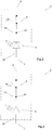
Figure 2 shows the circuit diagram of a single light sensitive microcell belonging to the photomultiplier device of the invention, in the state of inhibition of the interruption component; -
Figure 3 shows the circuit diagram of a single light sensitive microcell belonging to the photomultiplier device of the invention, in the state of conduction of the interruption component; -
Figure 4 shows the circuit diagram of a single light sensitive microcell according to an alternative embodiment to that shown inFigures 2 and 3 , in the state of inhibition of the interruption component; -
Figure 5 shows the circuit diagram related to the implementation of the single microcell represented inFigures 2 and 3 according to a first preferred embodiment of the invention; -
Figure 6 shows a sectional view of the light sensitive microcell ofFigure 5 ; -
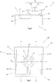
Figure 7 shows a topographic view of a set of four light sensitive microcells according to the first preferred embodiment of the photomultiplier device of the invention; -
Figure 8 shows an axonometric view of the photomultiplier device according to a second preferred embodiment of the invention; -
Figure 9 shows the circuit diagram related to the implementation of a single light sensitive microcell according to said second preferred embodiment of the photomultiplier device of the invention shown inFigure 8 ; -
Figure 10 shows a topographic view of a set of four microcells according to said second preferred embodiment of the photomultiplier device of the invention shown inFigure 8 ; -
Figure 11 shows a topographic view of a set of light sensitive microcells of the photomultiplier device of the invention connected to one another in such a way as to allow the reading of the rows/columns of the single light sensitive microcells; -
Figure 12 shows a sectional view of a possible implementation of the light sensitive microcell schematically shown inFigure 4 ; -
Figure 13 shows the circuit diagram relating to the implementation of a single light sensitive microcell comprising two reset MOS transistors in series and a reset capacitor. - The solid-state photomultiplier device or SiPM for detecting one or more photons that is the subject of the invention is represented as a whole, according to a first preferred embodiment, in
Figure 1 , where it is indicated by 1 and, according to a second preferred embodiment, inFigure 8 , where it is indicated by 100. - Concerning the first preferred embodiment, as shown in
Figure 1 , thephotomultiplier device 1 of the invention comprises asurface 2 that is sensitive to said photons F and created on asemiconductor substrate 3. Saidsensitive surface 2 is defined by a plurality of lightsensitive microcells 4 connected to one another in parallel in such a way as to supply a single common analog output signal Sout from thephotomultiplier device 1. For this reason, thephotomultiplier device 1 of the invention is considered a solid-state photomultiplier device of the analog type. - As can be observed in the circuit diagrams of
Figures 2 and 3 , each one of the lightsensitive microcells 4 comprises anavalanche photodiode 5 interposed between afirst electrode 6 and asecond electrode 7, which are configured so as to supply saidavalanche photodiode 5 with a reverse polarization voltage. Said polarization voltage, in particular, is higher than the breakdown voltage VBD of theavalanche photodiode 5 by a pre-defined value VOV. - According to the preferred embodiment of the
photomultiplier device 1 of the invention described herein and illustrated inFigure 6 , theavalanche photodiode 5 is carried out with n on p technology, according to which theaccumulation terminal 53 that accumulates the charge of the avalanche coincides with thecathode 51 of thesame avalanche photodiode 5. It cannot be excluded, however, that in an alternative embodiment of thephotomultiplier device 1 of the invention theavalanche photodiode 5 may be made with p on n technology, according to which theaccumulation terminal 53 that accumulates the charge of the avalanche coincides, instead, with theanode 52 of thesame avalanche photodiode 5. For this reason and for the sake of clarity, from this point onward, where not expressly specified otherwise the genericterm accumulation terminal 53 will be used to indicate thecathode 51 of the n on p photodiode and theanode 52 of the p on n photodiode. - According to the invention, each one of said light
sensitive microcells 4 comprises, furthermore, aninterruption component 8 intended to interrupt electric continuity and interposed between theaccumulation terminal 53 of thecorresponding avalanche photodiode 5 and saidfirst electrode 6. All of saidinterruption components 8 of the plurality of lightsensitive microcells 4 are configured in such a way as to simultaneously switch over from a state of conduction, schematically illustrated inFigure 2 , to a state of inhibition, illustrated inFigure 3 . Clearly, saidinterruption components 8 are configured also to be simultaneously switched over from said state of inhibition to the state of conduction. - In particular, said simultaneous switching operations of the
interruption components 8 are carried out, as explained in detail here below in the description of the preferred embodiment of thephotomultiplier device 1 of the invention, by means of a control signal Sc properly generated and sent to thesame interruption components 8 as an input signal. - Advantageously, this type of implementation makes it possible to provide a method for the control and operation of the
same photomultiplier device 1 according to an approach of the so-called "Passive Quenching - Active Recharge" or PQAR type. In other words, said control and operation method for controlling and operating thephotomultiplier device 1 of the invention allows the passive quenching of the avalanche effect generated in one or more of theavalanche photodiodes 5 belonging to the various lightsensitive microcells 4 and, at the same time, makes it possible to recharge the same lightsensitive microcells 4, and thus to reversely polarize saidphotodiodes 5, in a desired time instant, meaning in an active mode (Active Recharge). - Advantageously, according to this embodiment of the invention, the exploitation of said
interruption components 8 also as passive quenching circuits makes it possible to avoid the need to provide quenching resistors connected in series to thephotodiodes 5, and thus also makes it possible to reduce the production costs of thephotomultiplier device 1. - In order to better understand how this approach can be applied using the
photomultiplier device 1 of the invention, the initial situation should be considered, in which all of theavalanche photodiodes 5 of the lightsensitive microcells 4 are in a state of reverse polarization, meaning charged and ready to detect the absorption of a photon F. At the same time, theinterruption components 8 should be considered as being in the state of inhibition, as shown inFigure 3 . In this situation, following the impact of a photon F on one or more of saidavalanche photodiodes 5, said avalanche effect takes place in saidphotodiodes 5. This avalanche effect is quenched in a passive manner, following the discharge of the junction capacitance of theavalanche photodiode 5 until reaching voltage VBD, as theinterruption components 8, being in the state of inhibition, substantially behave as an open circuit and do not allow the current flow through the light sensitive microcell. In this condition, the single lightsensitive microcells 4 in which the avalanche effect was generated and quenched remain inhibited until thesame interruption components 8 are switched over to the state of conduction, that is, until thecorresponding avalanche photodiodes 5 are once again polarized reversely until reaching voltage VBD+VOV. - Once the simultaneous switching over of all the
interruption components 8 to the state of conduction has been activated, said lightsensitive microcells 4 on which said avalanche effect has occurred are recharged and return to an active state, like the other lightsensitive microcells 4 on which no photon F has impacted and, consequently, on which said avalanche has not occurred. Therefore, the entiresensitive surface 2 of thephotomultiplier device 1 is again in an active state, ready to detect the impact of one or more photons F on it. At this point, all of theinterruption components 8 are again simultaneously switched over to the state of inhibition in order to re-establish said initial condition. - Said simultaneous double switching over of the
interruption components 8, which from this point onwards will be referred to as "reset phase", is repeated every time interval T, whose value is properly selected based on the electrical characteristics and the use requirements of thephotomultiplier device 1. In practice, all of the lightsensitive microcells 4 are theoretically in an active state, meaning that they are capable of detecting a photon F that impacts their sensitive part, for a period of time that elapses between a reset phase and the successive one. - This type of approach implemented by means of the
photomultiplier device 1 of the invention makes it possible to obtain a series of advantageous technical effects that in turn allow the above mentioned objects of the invention to be achieved. - In particular, a first advantageous effect that is obtained through the implementation of said reset phase on the
photomultiplier device 1 of the invention lies in that the lightsensitive microcells 4 with a high level of DCR tend, immediately after each reset phase, to generate an avalanche effect independently of whether photons F impact them or not. Therefore, these lightsensitive microcells 4 do not contribute to the DCR of thephotomultiplier device 1 for most of the time during which thesame device 1 is sensitive to photons, that is, between a reset phase and the successive one. - At this point, it is important to underline that, in general, in the population of light
sensitive microcells 4 of a SiPM, it is common that a small portion of said microcells contributes to most of the DCR. - As already explained, for the reasons described above, the avalanche effects generated in said light
sensitive microcells 4 with a high level of DCR tend to be exhausted in a limited time. This effect, even if it involves the loss of part of the sensitive surface of thephotomultiplier device 1 due to the quenching of said lightsensitive microcells 4, limits the contribution of these latter lightsensitive microcells 4 to the total noise of thesame photomultiplier device 1 to a small fraction of the period during which the sensitive surface is in the active state. Therefore, to advantage, once said very noisy lightsensitive microcells 4 have been quenched, a fair comprise is obtained between the efficiency (intended as "Photo Detection Efficiency" or PDE) of thephotomultiplier device 1, which decreases, and the noisiness of the same device. - Advantageously, in this way an effect is automatically produced that is similar to the programmable quenching of the more noisy light sensitive microcells in a photomultiplier device of the digital type.
- Moreover, a further advantageous effect that is obtained with the use of the
photomultiplier device 1 of the invention is the considerable reduction, if not the elimination, of the phenomenon of "Afterpulsing". In fact, as following the generation of the avalanche effect in a single lightsensitive microcell 4 this microcell remains inhibited until the successive reset phase, by selecting a suitable reset interval T it is possible to inhibit a further generation of avalanche effect on the same lightsensitive microcell 4 due to the phenomenon of Afterpulsing. From this point of view, the resulting effect is very similar to the effect obtained with an active quenching circuit, as described above. Even for this reason, advantageously, a fair compromise is obtained between the efficiency of thephotomultiplier device 1 of the invention and the noise level of the same. - According to the preferred embodiment of the
photomultiplier device 1 of the invention, the first and thesecond electrode sensitive microcells 4, in such a way as to provide thecorresponding avalanche photodiodes 5 with a common reverse polarization voltage. Furthermore, according to the preferred embodiment of the invention, each one of saidinterruption components 8, as can be observed inFigure 5 , is areset MOS transistor 10 connected, by means of itssource terminal 11, to theaccumulation terminal 53 of theavalanche photodiode 5, which in the case at hand corresponds to thecathode 51 of thesame photodiode 5, and to thefirst electrode 6 by means of itsdrain terminal 12. Furthermore, all of thereset MOS transistors 10 of the plurality of lightsensitive microcells 4 have theirgate terminals 13 connected together. Saidgate terminals 13, furthermore, are configured in such a way as to receive said impulse control signal Sc as an input, so as to control the simultaneous switching over of the samereset MOS transistors 10 from said state of conduction to the state of inhibition and vice versa and, consequently, in such a way as to carry out the reset phase described above. - According to an alternative embodiment of the light
sensitive microcells 4 described herein and illustrated inFigures 2 and 3 , aquenching component 9 can be interposed between theinterruption component 8 and thefirst electrode 6, as can be observed inFigure 4 . The presence of saidquenching component 9, advantageously, makes it possible to quench any avalanche effect that may be generated in the lightsensitive microcells 4 during the reset phase, meaning when theinterruption component 8 is in the state of conduction and therefore cannot stop this phenomenon. - Preferably but not necessarily, said quenching
component 9 is implemented through a quenchingresistor 9. - Furthermore, according to a preferred embodiment of the invention, said quenching
resistor 9 is made of silicon, with a layer of the same type as that of the surface layers n+ (or p+), and subjected to suitable doping to obtain the desired resistance value. In this way the quenchingresistor 9 can be carried out as a single piece with the layer corresponding to thesource terminal 11 of thereset MOS transistor 10 or replace it, as shown inFigure 12 , or, according to a further variant embodiment, replace the layer corresponding to thedrain terminal 12. Advantageously, in this manner the quenchingresistor 9 is made with a single additional layer and with just one additional lithographic mask with respect to the standard process according to which only thereset MOS transistor 10 is provided. - It cannot be excluded that in different embodiments of the
photomultiplier device 1 of the invention saidquenching component 9 can be implemented in another way, different from a quenching resistor, provided that it is capable of quenching any avalanche effect that may occur during said reset phase. - In this regard, it is important to highlight that which happens in a
photodiode 5 when, during a reset phase of thephotomultiplier device 1, an avalanche occurs. In this situation, the number of carriers that pass through the junction of thephotodiode 5 during the avalanche - also called the "gain" of the avalanche - is much higher compared to "normal" events, considering that the avalanche current is not stopped by the quenching effect. - Consequently, also the number of photons F emitted by the hot carriers and the probability of occurrence of Optical Crosstalk among the light
sensitive microcells 4 is proportionally higher. Therefore, if an avalanche occurs in a lightsensitive microcell 4 during the reset phase, it is highly probable that other avalanches will occur also in the adjacent lightsensitive microcells 4 and generate further avalanches, until all of the lightsensitive microcells 4 of thephotomultiplier device 1 are affected. - The result of this process is that the
entire photomultiplier device 1 is not sensitive to light until the beginning of the successive reset phase. The probability that this will occur depends, in a first approximation, on the DCR, on the duration of the reset phase, on the reset interval T and on the overvoltage. Therefore, the presence of saidquenching component 9, and in particular of the quenchingresistor 9, advantageously makes it possible to avoid said concatenation of effects. - In practice, according to the preferred embodiment of the invention described herein, in the
photomultiplier device 1 the lightsensitive microcells 4 are provided on saidsingle semiconductor substrate 3. In particular, preferably but not necessarily, saidsemiconductor substrate 3 comprises anepitaxial substrate 14 superimposed to a highly doped layer. - As can be observed in
Figure 6 , in the preferred embodiment of thephotomultiplier device 1 thep-n junction 15 of theavalanche photodiode 5 is defined on saidsemiconductor substrate 3 for each lightsensitive microcell 4, said junction, as explained above, being carried out according to n on p technology. - Always according to said first preferred embodiment of the invention, said
p-n junction 15 features, in particular, afirst layer 16 subjected to doping of type p+, above which asecond layer 17 is defined that is subjected to doping of type n+. In particular, saidsecond layer 17 serves both ascathode 51, and therefore asaccumulation terminal 53, of theavalanche photodiode 5, and assource terminal 11 of thereset MOS transistor 10. Athird layer 18 is furthermore defined on thesemiconductor substrate 3, said third layer being spaced from saidp-n junction 15 and subjected to doping of type n+, meaning the same type of doping of saidsecond layer 17, in such a way as to define thedrain terminal 12 of therest MOS transistor 10. - As explained above, it cannot however be excluded that in an alternative embodiment of the
photomultiplier device 1 of the invention, thep-n junction 15 of theavalanche photodiode 5 may be made with p on n technology. In this case, thefirst layer 16 is subjected to doping of type n+, while said second andthird layers - Concerning the
gate terminal 13 of therest MOS transistor 10, as can be observed inFigure 6 this is superimposed to thesemiconductor substrate 3 between thep-n junction 15 and thethird substrate 18. Saidgate terminal 13 preferably comprises ametal layer 131. - Advantageously, this solution makes it possible to obtain the
avalanche photodiode 5 and thereset MOS transistor 10 of each one of the lightsensitive microcells 4 occupying a smaller area of the surface of thephotomultiplier device 1 compared to the area that would be occupied by a photodiode and a separate MOS transistor. Therefore, this embodiment of the single lightsensitive microcell 4 shown inFigure 6 makes it possible to maintain a high Fill Factor value for theentire photomultiplier device 1, notwithstanding the introduction of an active component, like thereset MOS transistor 10. - Furthermore, according to the preferred embodiment of the invention described herein and represented in
Figure 6 , thesource terminal 11 and thedrain terminal 12 of thereset MOS transistor 10 are preferably but not necessarily carried out substantially exploiting the same layer n+ that allows theaccumulation terminal 53 of theavalanche photodiode 5 to be defined. Therefore, this implementation, advantageously, does not increase the complexity of the process required to make said lightsensitive microcell 4. - At this point of the description it is important to underline that the structure of the single light
sensitive microcell 4 shown inFigure 6 makes it possible to obtain advantages that are independent of the overall structure and the specific operation of thephotomultiplier device 1 of the invention described above. Therefore, said characteristics of the lightsensitive microcell 4 that have just been described above may even be claimed, independently of said overall structure of thephotomultiplier device 1 that is the object of the present invention and of the related control and operation method. - Furthermore, in order to maintain a high Fill Factor value for the
photomultiplier device 1 of the invention, the latter comprises a plurality of sets of lightsensitive microcells 50 located side by side, wherein each one of said sets 50, as shown inFigure 7 , comprises four of said lightsensitive microcells 4. In particular, the four lightsensitive microcells 4 that make up each one of said foursets 50, according to the topographic view ofFigure 7 , are grouped inside a quadrangular area A. In greater detail, in said quadrangular area A it is possible to identify thep-n junctions 15 of the four lightsensitive microcells 4, carried out so that they are adjacent in pairs at the level of the sectors A1 defined by the intersection of two axes D passing through the same quadrangular area A. As already explained above, eachp-n junction 15 defines theavalanche photodiode 5 and thesource terminal 11 of thereset MOS transistor 10 of one of the four lightsensitive microcells 4. As can be observed always inFigure 7 , thedrain terminals 12 of thereset MOS transistors 10 are carried out as a single element defined in the point P of intersection of the two axes D. - Furthermore, according to the preferred embodiment of the invention described herein, the
gate terminals 13 of thereset MOS transistors 10 are connected together and are superimposed to saidsemiconductor substrate 3 between thecommon drain terminal 12 and thesource terminal 11. Finally, preferably but not necessarily, thephotomultiplier device 1 of the invention comprises electric insulation elements provided along the axes D and on the perimeter of the quadrangular area A, in such a way as to electrically insulate from one another thep-n junctions 15 of the adjacent lightsensitive microcells 4. - Also in this case, the advantages obtained thanks to this special structure of the
set 50 comprising four lightsensitive microcells 4 are independent of the overall structure and the specific operation of thephotomultiplier device 1 of the invention described above. Therefore, also in this case, said characteristics of theset 50 may even be the subject of a claim, independently of the overall structure of thephotomultiplier device 1 that is the subject of the present invention and of the related control and operation method. - According to the preferred embodiment of the
photomultiplier device 1 described herein, the reading of the analog output signal Sout generated by thephotomultiplier device 1 of the invention is carried out by means of the AC coupling technique through thegate terminals 13 of thereset MOS transistors 10, which are connected together, or through the Back of thesame photomultiplier device 1. - Advantageously, the extraction of the signal Sout by means of said AC coupling technique allows the signal to be read rapidly ("fast timing"), given that the latter has a wave shape that is substantially equal to the derivative of a step signal and therefore very short and without undershoot.
- Alternatively, said reading may also be made in DC through the
drain terminals 12, always of thereset MOS transistors 10 belonging to thephotomultiplier device 1 of the invention. - In this way, the information on the light
sensitive microcells 4 that switched over during the reset interval T is maintained in thephotomultiplier device 1 until the beginning of the successive reset cycle, when it is read. - A possible further application of this method for storing the signal and reading the same in DC relates to the reading of the rows/columns of the single light
sensitive microcells 4 or of subsets of microcells of thephotomultiplier device 1. - A typical subdivision may lead to the division of the active area of the
photomultiplier device 1 into a grid of smaller sub-SiPMs. As can be observed inFigure 11 , thedrain terminals 12 of thereset MOS transistors 10 of themicrocells 4 of each column of sub-SiPMs are connected together, like thegate terminals 13 of each row of the sub-SiPM. In the instant when the reading in DC is performed, at the end of the reset interval T, thevarious gate terminals 13 are enabled in sequence, so that the charge stored in the sub-SiPM corresponding to thegate terminal 13 enabled in that precise moment and to therelated drain terminal 12 exits from each column constituted by thedrain terminals 12 connected together. Eachdrain terminal 12 is associated with a separate reading channel. In this way, to advantage, only n reading channels are needed to read an array of n x n sub-SiPMs. Alternatively, a further method for reading rows/columns may include the connection of all of thedrain terminals 12 together to a single reading channel. According to this method, therefore, two MOS transistors in series are used for each lightsensitive microcell 4, as can be observed inFigure 13 , said MOS transistors being connected to twocontrol gate terminals 13 that are distinct from each other. The twocontrol gate terminals 13 are respectively connected by rows and by columns, obtaining the effect that the rows/columns are read from thedrain terminals 12 with a single reading channel, but requiring more time (n x n x Tread, where Tread is the time needed to read/reset a sub-SiPM). - It cannot be excluded, furthermore, that the reading of rows/columns of the individual light
sensitive microcells 4, carried out by means of thephotomultiplier device 1 of the invention, may be implemented in a way different from those described above. - As previously explained, a second embodiment of the
photomultiplier device 1 of the invention is shown inFigure 8 , where it is indicated by 100. - Said
photomultiplier device 100 is distinguished from the first embodiment of the invention described above due to the fact that each individual lightsensitive microcell 4, as shown inFigure 9 , comprises also anextraction capacitor 19 coupled with thecorresponding avalanche photodiode 5 and configured in such a way as to allow the reading, from a first terminal of its own, of the output signal Sout through said AC coupling technique. This solution, advantageously, makes it possible to simplify the reading operations, considerably reducing any interference between the impulse control signal Sc and said output signal Sout. - Preferably, according to said second embodiment of the
device 100 of the invention, saidextraction capacitor 19 is made with MOS technology, so that said reading terminal corresponds to the plate of saidcapacitor 19 constituted by the so-calledconductor side 22 of the MOS, while the second plate of theextraction MOS capacitor 19 is defined by thesemiconductor side 20. Preferably, theconductor side 22 is made of a metallic material. It cannot be excluded, however, that saidconductor side 22 be made, for example, in polysilicon or any other material, provided that it is a conductor material. - In even greater detail, the
conductor side 22 of theextraction MOS capacitor 19 is electrically insulated from thegate terminal 13 of thereset MOS transistor 10. - Furthermore, the
semiconductor side 20 of theextraction MOS capacitor 19 corresponds to theaccumulation terminal 53 of thephotodiode 5, and thus to thesource terminal 11 of thereset MOS transistor 10. - Following this approach it is possible to make a relatively small
reset MOS transistor 10, to induce a reduced disturbance, and a largeextraction MOS capacitor 19, in order to collect the signal Sout as effectively as possible. Optionally, in order to reduce the number of connections towards the outside of thephotomultiplier device 100, theconductor side 22 of theextraction MOS capacitor 19 and thedrain terminal 12 of thereset MOS transistor 10 can be connected together. In fact, the signal Sout in AC travels through theextraction MOS capacitor 19 when the reset is not active, while the reset control signal Sc travels in thedrain terminal 12 during the reset cycle, and therefore the two signals Sout and Sc are temporally separated. - Furthermore, in said second embodiment of the
photomultiplier device 100 of the invention, in each one of said lightsensitive microcells 4 theconductor side 22 of theextraction MOS capacitor 19 is created, as is clearly explained below, along the boundary lines between the same lightsensitive microcell 4 and the adjacent lightsensitive microcell 4. - This last characteristic of the
photomultiplier device 100 of the invention makes it possible to exploit theconductor side 22 also or exclusively in the case in which the reading of the signal Sout is not carried out through saidconductor side 22, as an electric insulation element between two adjacent lightsensitive microcells 4. - In particular, in the case where the
MOS capacitor 19 is used exclusively to obtain electric insulation between the various adjacent lightsensitive microcells 4 and between each one of them and thedrain terminal 12 of theMOS transistor 10, thesemiconductor side 20 of thesame MOS capacitor 19 may correspond, as an alternative to saidsource terminal 11 of saidMOS transistor 10, to saiddrain terminal 12. - In both cases, to obtain said insulation, the
MOS capacitor 19 is properly polarized in DC, in such a way as to modify the potential of silicon between the doped layers on which theconductor side 22 is made. - Advantageously, in the case of the preferred embodiment described herein, according to which the
p-n junctions 15 of theavalanche photodiode 5 are made with n on p technology, said implementation of insulation among lightsensitive microcells 4 is more efficient from the point of view of the space occupied compared, for example, to the known technique that in technical jargon is called "p-stop". By the way, in the alternative case in which saidp-n junctions 15 were made with p on n technology, said known technique would be of the "n-stop" type. Concerning, again, the implementation of insulation by means of saidMOS capacitor 19, this is more economic than the above mentioned "p-stop" or "n-stop" techniques. - As in the case of the
photomultiplier device 1 of the first preferred embodiment of the invention, in order to maintain a high Fill Factor value and at the same time obtain all of the advantages described up to now, also thephotomultiplier device 100 of the invention preferably but not necessarily comprises a plurality ofadjacent sets 50 of lightsensitive microcells 4. In particular, each one of said sets 50, as can be observed in the topographic view shown inFigure 10 , comprises four lightsensitive microcells 4 grouped inside a quadrangular area A. In said quadrangular area A it is possible to identify thep-n junctions 15 of the four lightsensitive microcells 4 adjacent in pairs at the level of the sectors A1 defined by the intersection of two axes D passing through the same quadrangular area A. Each one of thep-n junctions 15, as already explained above, defines theavalanche photodiode 5, thesource terminals 11 of thereset MOS transistor 10 and thesemiconductor side 20 of theextraction MOS capacitor 19 of one of the lightsensitive microcells 4. Furthermore, also in this case thedrain terminals 12 of thereset MOS transistors 10 are made as a single element defined in the point P of intersection of said two axes D. Furthermore, as can be observed always inFigure 10 , theconductor side 22 of theextraction MOS capacitor 19 of each one of the lightsensitive microcells 4 is shared by the adjacent lightsensitive microcell 4 along the portion of each axis D interposed between the corresponding twop-n junctions 15. - This implementation, as explained above, advantageously makes it possible to use said
MOS capacitor 19 to insulate the adjacent lightsensitive microcells 4 and, furthermore, to insulate each one of them and thedrain terminal 12 of thereset MOS transistor 10 in the areas, indicated by B inFigure 10 , in which thegate terminal 13 of thesame reset transistor 10 is not present between theavalanche photodiode 5 of the lightsensitive microcell 4 and saiddrain terminal 12. In order to obtain said insulation, theMOS capacitor 19 is properly polarized in DC, in such a way as to modify the potential of silicon among the doped layers on which theconductor side 22 is made. - In the same way, the
gate terminal 13 of thereset MOS transistor 10 of each one of the lightsensitive microcells 4 is made in the space defined within the sector A1 of the correspondingp-n junction 15 between the adjacent and intersecting portions of the two axes D. Furthermore, each one of saidgate terminals 13 is superimposed to saidsemiconductor substrate 3 between thedrain terminal 12 and thesource terminal 11 of the lightsensitive microcell 4. Once again it is important to underline that the advantages obtained thanks to said special structure of theset 50 comprising four lightsensitive microcells 4 are independent of the overall structure and of the specific operation of thephotomultiplier device 100 of the invention described above. Therefore, also in this case, these characteristics of theset 50 may even be claimed, independently of the overall structure of thephotomultiplier device 100 that is the subject of the present invention and of the related control and operation method. - As already explained, the invention also includes the method for controlling the
photomultiplier devices interruption component 8 connected in series to theavalanche photodiode 5 of each one of the lightsensitive microcells 4. The control method, according to the invention, controls the simultaneous switching over of saidinterruption components 8 of the plurality of lightsensitive microcells 4 from the state of inhibition to the state of conduction, in such a way as to impose the desired reverse polarization voltage between thecathode 51 and theanode 52 of each one of theavalanche photodiodes 5. Furthermore, in sequence, the method that is the subject of the invention controls the simultaneous switchover of theinterruption components 8 of said plurality of lightsensitive microcells 4 from the state of conduction to the state of inhibition, in such a way as to electrically insulate each one of theavalanche photodiodes 5 from thefirst electrode 6. In this condition of reverse polarization, theavalanche photodiodes 5, as described above, are configured to generate an avalanche current in the case where one or more photons F impact on them. According to the method of the invention, said two switching over operations carried out in sequence, previously defined also as reset phases, are repeated at pre-defined time intervals T, whose duration is properly selected based on the electrical characteristics and use requirements of thephotomultiplier device gate terminals 13, connected together, of thereset MOS transistors 10 of thephotomultiplier device - In greater detail, the switching over from the state of inhibition to the state of conduction is carried out at the level of the rising edge of the impulse of the impulse control signal Sc, while the switching over of the
reset MOS transistors 10 from the state of conduction to the state of inhibition is carried out at the level of the falling edge of the same impulse. - Considering the phenomenon of the avalanches that occur during the reset phase, as described above, a method for reducing its effect on the
photomultiplier device interruption components 8 are in the state of conduction, into two or more shorter sub-cycles to be rapidly carried out in sequence, in such a way as to cover the same duration of the reset cycle. The minimum value of the entire duration of the reset cycle is selected in advance, in order to obtain a complete recharge of theavalanche photodiodes 5. In this way, if an avalanche occurs in one ormore avalanche photodiodes 5 during a reset sub-cycle, this is advantageously quenched at the end of the same sub-cycle and not at the end of the entire reset cycle. Therefore, the average duration of the avalanches that occur during the reset phase is advantageously reduced and consequently also the average number of photons F emitted for each one of them is reduced. Consequently, the probability that said negative phenomenon may end with inhibiting theentire photomultiplier device - An alternative method for reducing the effect of the avalanches that occur during the reset phase consists in adding, to each light
sensitive microcell 4, asecond interruption component 30, as can be observed inFigure 13 , between thefirst interruption component 8, represented inFigures 2 and 3 , and thefirst electrode 6, as well as acapacitor 60 connected with a first plate of its own between said twointerruption components interruption components interruption component 30 is switched over from the state of inhibition to the state of conduction, charging thecapacitor 60 at the reset voltage, which corresponds to the polarization to be imposed to theaccumulation terminal 53 of thephotodiode 5. In a successive stage theinterruption component 30 is switched over to the state of inhibition again and theinterruption component 8 is switched over to the state of conduction, so that the charge stored in thecapacitor 60 is transferred to theaccumulation terminal 53, restoring the above mentioned polarization voltage. During the time interval T between a reset cycle and the successive one, theinterruption component 30 can remain in the state of conduction, maintaining thecapacitor 60 charged at the reset voltage. In this way, saidcapacitor 60 is already charged at the beginning of the successive reset cycle. Depending on the value of thecapacitor 60, a single reset cycle may not be sufficient to recharge theaccumulation terminal 53 at a voltage that is sufficiently near to the desired one. In this case, it is possible to repeat an n number of sequential reset sub-cycles, until obtaining the desired charge of theaccumulation terminal 53. With said implementation illustrated inFigure 13 , in the case where an avalanche should occur while theinterruption component 8 is in the state of conduction, the same avalanche would be quenched in any case, as theinterruption component 30 is in the state of inhibition. The gain is higher than that of a "normal" event, as the avalanche discharges thecapacitor 60 beyond the capacity of thephotodiode 5, but in general it is much lower than the gain that would result if the avalanche taking place during the reset phase were not quenched. - As can be observed always in
Figure 13 , according to a possible implementation of the circuit, both theinterruption components MOS transistors reset MOS transistor 10 shown inFigure 6 . In particular, it is possible to use the same layer n+ of thephotodiode 5 to implement also thesource terminals drain terminals MOS transistors source terminal 11 related to theMOS transistor 10 is melted with theaccumulation terminal 53 of thephotodiode 5, while thedrain terminal 12 of thesame MOS transistor 10 is melted with thesource terminal 31 of theMOS transistor 30, advantageously obtaining a very compact and efficient structure in terms of area consumption. Thecapacitor 60 can simply be the capacity of thesource terminal 31 of theMOS transistor 30 and of thedrain terminal 12 of theMOS transistor 10 to earth. - The
capacitor 60 and theMOS transistor 30 can also be shared by sets ofmicrocells 4, for the purpose of saving more active area and obtain higher values for thecapacitor 60, which allow a more complete reset of thephotodiode 5 for each reset sub-cycle. Furthermore, if thecapacitor 60 is shared amongseveral microcells 4 of the same set, thosemicrocells 4 in which no avalanche occurred in the previous reset interval T are already polarized at the reset voltage and the capacity of theirphotodiodes 5 contributes, in parallel to thecapacitor 60, to recharging thephotodiodes 5 of themicrocells 4 that on the contrary switched over in the previous reset interval. - Going back to the control method that is the subject of the invention, as already stated above, according to a first preferred embodiment of the invention it includes the extraction of the common output signal Sout through the AC coupling technique on the
gate terminal 13 of thereset MOS transistor 10 or from the Back of thephotomultiplier device photomultiplier device 100, on theconductor side 22 of theextraction MOS capacitor 19. - It cannot be excluded, however, that in the method of the invention the extraction of the common output signal Sout is carried out through the DC reading technique from the
drain terminal 12 of thereset MOS transistor 10. - This last implementation would make it possible to read the charge, meaning the number of light
sensitive microcells 4 in which an avalanche took place in the reset interval T, at the end of said interval T, according to the procedures previously described in detail. - According to the above, it can therefore be understood that the photomultiplier device of the invention and the related control method achieve all the set objects.
- In particular, the invention achieves the object to provide a photomultiplier device of the analog type that following a recharge phase of the entire light sensitive surface is capable of automatically and rapidly inhibiting those light sensitive microcells that are considered highly noisy, that is, the microcells having a high "Dark Count Rate".
- The invention also achieves the object to provide a photomultiplier device that is capable of limiting, if not eliminating, the so-called "Afterpulsing" phenomenon in the individual light sensitive microcells.
- The invention achieves the further object to provide a photomultiplier device that, considering light sensitive microcells having the same size, makes it possible to increase the FF compared to the photomultiplier devices of the known art, or that makes it possible to reduce the size of the light sensitive microcells though maintaining a high FF value.
- The invention also achieves the object to provide a photomultiplier device whose production efficiency is better than that of the photomultipliers of the known art, thanks to the fact that a smaller number of rejects is generated during production.
- Finally, the invention achieves the object to provide a photomultiplier device of the analog type integrating those structural and functional characteristics, typical of digital photomultiplier devices, that make it possible to obtain the advantages defined above while at the same time maintaining a lower production cost compared to said digital devices.
Claims (14)
- Solid-state photomultiplier device (SiPM) (1) for detecting one or more photons (F), of the type comprising a surface (2) sensitive to said photons (F) and created on a semiconductor substrate (3), said sensitive surface (2) being defined by a plurality of light sensitive microcells (4) connected to one another in parallel in such a way as to send out a common analog output signal (Sout), each one of said light sensitive microcells (4) comprising an avalanche photodiode (5) interposed between a first electrode (6) and a second electrode (7) suited to supply said avalanche photodiode (5) with a reverse polarization voltage, characterized in that for each one of said light sensitive microcells (4) it comprises an interruption component (8) suited to interrupt electrical continuity and interposed between the accumulation terminal (53) that accumulates the avalanche charge of said avalanche photodiode (5) and said first electrode (6), said interruption components (8) of said plurality of light sensitive microcells (4) being configured so as to simultaneously switch over from a state of conduction to a state of inhibition or vice versa.
- Photomultiplier device (1) according to claim 1, characterized in that for each one of said light sensitive microcells (4) it comprises a quenching component (9) interposed between said interruption component (8) and said first electrode (6).
- Photomultiplier device (1) according to any of the preceding claims, characterized in that said first electrode (6) and said second electrode (7) are shared by said plurality of light sensitive microcells (4), in such a way as to supply said avalanche photodiodes (5) of said plurality of light sensitive microcells (4) with a common reverse polarization voltage.
- Photomultiplier device (1) according to any of the preceding claims, characterized in that each one of said interruption components (8) is a reset MOS transistor (10) connected to said accumulation terminal (53) of said avalanche photodiode (5) with its source terminal (11) and to said first electrode (6) with its drain terminal (12), the gate terminals (13) of said reset MOS transistors (10) of said plurality of light sensitive microcells (4) being connected together and being configured to receive an impulse control input signal (Sc) for the simultaneous switchover of said reset MOS transistors (10) from said conduction state to said inhibition state or vice versa.
- Photomultiplier device (1) according to claim 4, characterized in that each one of said light sensitive microcells (4) is created on said semiconductor substrate (3), the following being defined in said semiconductor substrate:- the p-n junction (15) of said avalanche photodiode (5) defined by a first layer (16) subjected to a first doping type, p+ or n+, above which a second layer (17) is defined that is subjected to an opposite doping type, n+ or p+, with respect to said first layer (16), said second layer (17) serving both as accumulation terminal (53) of said avalanche photodiode (5) and as source terminal (11) of said reset MOS transistor (10);- a third layer (18) carried out so that it is spaced from said p-n junction (15) and subjected to a doping type, n+ or p+, corresponding to said second layer (17) so as to serve as drain terminal (12) of said reset MOS transistor (10);- the gate terminal (13) of said reset MOS transistors (10), carried out so that it is superimposed to said semiconductor substrate (3) between said p-n junction (15) and said third layer (18).
- Photomultiplier device (1) according to claim 4 or 5, characterized in that each one of said light sensitive microcells (4) comprises an extraction MOS capacitor (19) coupled with said avalanche photodiode (5) and configured to allow the extraction of said output signal (Sout) from its conductor side (22) through the AC coupling technique.
- Photomultiplier device (1) according to claim 6, characterized in that for each one of said light sensitive microcells (4):- the semiconductor side (20) of said extraction MOS capacitor (19) coincides with said source terminal (11) of said reset MOS transistor (10);- said conductor side (22) of said extraction MOS capacitor (19) is electrically insulated from said gate terminal (13) of said reset MOS transistor (10).
- Photomultiplier device (1) according to claim 7, characterized in that for each one of said light sensitive microcells (4):- said conductor side (22) of said extraction MOS capacitor (19) is carried out along the boundary lines between said light sensitive microcell (4) and the adjacent light sensitive microcell (4) and/or between the p-n junctions (15) and the drain terminal (12) of the reset transistor (10) of each one of said light sensitive microcells (4) so as to serve as an electric insulation element.
- Photomultiplier device (1) according to claim 4 or 5, characterized in that it comprises at least one set (50) comprising four of said light sensitive microcells (4) grouped together, according to a topographic view of said set (50), inside a quadrangular area (A) in which it is possible to identify:- said p-n junctions (15) carried out so that they are adjacent in pairs at the level of the sectors (A1) defined by the intersection of two axes (D) passing inside said quadrangular area (A), each one of said p-n junctions (15) defining said avalanche photodiode (5) and said source terminal (11) of said reset MOS transistor (10) of one of said light sensitive microcells (4);- said drain terminals (12) carried out as a single piece defined in the point (P) of intersection of said two axes (D);- said gate terminals (13) connected together and superimposed to said semiconductor substrate (3) between said drain terminals (12) and said source terminals (11).
- Photomultiplier device (1) according to any of the claims from 6 to 8, characterized in that it comprises at least one set (50) comprising four of said light sensitive microcells (4) grouped together, according to a topographic view of said set (50), inside a quadrangular area (A) in which it is possible to identify:- said p-n junctions (15), carried out so that they are adjacent in pairs at the level of the sectors (A1) defined by the intersection of two axes (D) passing inside said quadrangular area (A), each one of said p-n junctions (15) defining said avalanche photodiode (5), said source terminal (11) of said reset MOS transistors (10) and said semiconductor side (20) of said extraction MOS capacitor (19) of one of said light sensitive microcells (4);- said drain terminals (12) of said reset MOS transistors (10), created as single pieces defined in the point (P) of intersection of said two axes (D);- said conductor side (22) of the extraction MOS capacitor (19) of each one of said light sensitive microcells (4), carried out in common with the adjacent light sensitive microcell (4) along the portion of axis (D) interposed between the two corresponding p-n junctions (15) and/or between each one of said p-n junctions (15) and said drain terminal (12) of said reset transistor (10);- the gate terminal (13) of the reset MOS transistor (10) of each one of said light sensitive microcells (4), carried out in the space defined inside the sector (A1) of the corresponding p-n junction (15) between said two adjacent axes (D) intersecting each other.
- Method for controlling a photomultiplier device (1, 100) of the type according to any of the preceding claims, characterized in that it includes the following operations:- controlling the simultaneous switchover of said interruption components (8) of said plurality of light sensitive microcells (4) from said state of inhibition to said state of conduction, in such a way as to restore the reverse polarization voltage between the cathode (51) and the anode (52) of each one of said avalanche photodiodes (5);- controlling the simultaneous switchover of said interruption components (8) of said plurality of light sensitive microcells (4) from said state of conduction to said state of inhibition, in such a way as to electrically insulate each one of said avalanche photodiodes (5) from said first electrode (6), said avalanche photodiodes (5) being configured to generate an avalanche current in case of impact of one or more of said photons (F);- repeating said switchovers according to pre-established time intervals (T).
- Control method according to claim 11, characterized in that it controls said switchover operations through the application of an impulse control input signal (Sc) lasting for said pre-established time interval (T) to said gate terminals (13), connected together, of said reset MOS transistors (10) of the photomultiplier device (1, 100) according to any of the claims from 4 to 11, said switchover from said state of inhibition to said state of conduction being carried out at the level of the rising edge of the impulse of said impulse control signal (Sc) and said switchover from said state of conduction to said state of inhibition being carried out at the level of the falling edge of the impulse.
- Control method according to any of the claims 11 or 12, characterized in that the extraction of said common output signal (Sout) is carried out through the AC coupling technique on said gate terminal (13) of said reset MOS transistor (10), or on the Back of said photomultiplier device (1, 100), or on said conductor side (22) of said extraction MOS capacitor (19).
- Control method according to any of the claims 11 or 12, characterized in that the extraction of said common output signal (Sout) is carried out through the DC reading technique from said drain terminal (12) of said reset MOS transistor (10) at the end of said reset interval (T).
Applications Claiming Priority (2)
| Application Number | Priority Date | Filing Date | Title |
|---|---|---|---|
| IT000263A ITVI20130263A1 (en) | 2013-10-25 | 2013-10-25 | PHOTOMOLTIPER DEVICE AT THE STATE OF SOLID PERFORMANCE AND METHOD OF CONTROL OF SUCH PHOTOMOLTIPLICATOR DEVICE |
| PCT/IB2014/065566 WO2015059663A1 (en) | 2013-10-25 | 2014-10-23 | Improved solid-state photomultiplier device and method for controlling said photomultiplier device |
Publications (2)
| Publication Number | Publication Date |
|---|---|
| EP3061132A1 EP3061132A1 (en) | 2016-08-31 |
| EP3061132B1 true EP3061132B1 (en) | 2017-11-15 |
Family
ID=49684028
Family Applications (1)
| Application Number | Title | Priority Date | Filing Date |
|---|---|---|---|
| EP14806724.2A Active EP3061132B1 (en) | 2013-10-25 | 2014-10-23 | Improved solid-state photomultiplier device and method for controlling said photomultiplier device |
Country Status (3)
| Country | Link |
|---|---|
| EP (1) | EP3061132B1 (en) |
| IT (1) | ITVI20130263A1 (en) |
| WO (1) | WO2015059663A1 (en) |
Families Citing this family (3)
| Publication number | Priority date | Publication date | Assignee | Title |
|---|---|---|---|---|
| US11356628B2 (en) | 2017-10-31 | 2022-06-07 | Sony Semiconductor Solutions Corporation | Imaging apparatus and imaging system |
| JP7098559B2 (en) * | 2019-03-14 | 2022-07-11 | 株式会社東芝 | Photodetector and lidar device |
| US11428826B2 (en) | 2019-09-09 | 2022-08-30 | Semiconductor Components Industries, Llc | Silicon photomultipliers with split microcells |
Family Cites Families (3)
| Publication number | Priority date | Publication date | Assignee | Title |
|---|---|---|---|---|
| DE102010041805B4 (en) * | 2010-09-01 | 2018-03-22 | Siemens Medical Solutions Usa, Inc. | Device with a plurality of line or matrix-shaped photosensitive microcells |
| KR101814603B1 (en) * | 2011-06-16 | 2018-01-05 | 삼성전자주식회사 | Pixel device, and radiation detecting module and apparatus having the same |
| DE102012204806B4 (en) * | 2012-03-26 | 2013-10-17 | Siemens Aktiengesellschaft | Device with a variety of microcells |
-
2013
- 2013-10-25 IT IT000263A patent/ITVI20130263A1/en unknown
-
2014
- 2014-10-23 EP EP14806724.2A patent/EP3061132B1/en active Active
- 2014-10-23 WO PCT/IB2014/065566 patent/WO2015059663A1/en not_active Ceased
Non-Patent Citations (1)
| Title |
|---|
| None * |
Also Published As
| Publication number | Publication date |
|---|---|
| EP3061132A1 (en) | 2016-08-31 |
| WO2015059663A1 (en) | 2015-04-30 |
| ITVI20130263A1 (en) | 2015-04-26 |
Similar Documents
| Publication | Publication Date | Title |
|---|---|---|
| US11056525B2 (en) | Semiconductor photomultiplier | |
| US9109953B2 (en) | Photodetector and computed tomography apparatus | |
| US10276610B2 (en) | Semiconductor photomultiplier | |
| US8421172B2 (en) | Simplified silicon drift detector and wraparound neutron detector | |
| US8269181B2 (en) | Avalanche pixel sensors and related methods | |
| US9121766B2 (en) | Multi pixel photo detector array of Geiger mode avalanche photodiodes | |
| US9040898B2 (en) | Device having a plurality of photosensitive microcells arranged in row or matrix form | |
| US9664558B2 (en) | Sub-band infra-red irradiation for detector crystals | |
| US20150340390A1 (en) | Semiconductor photomultiplier | |
| JP7414306B2 (en) | Reducing optical crosstalk effects in SiPM | |
| JP6298234B2 (en) | Semiconductor structure for radiation detector and radiation detector | |
| WO2015059663A1 (en) | Improved solid-state photomultiplier device and method for controlling said photomultiplier device | |
| US11710798B2 (en) | Selenium photomultiplier and method for fabrication thereof | |
| CN110998874B (en) | Light emitting semiconductor device for generating short light pulses | |
| EP2740154A1 (en) | Semiconductor detector device | |
| KR20080074084A (en) | High Sensitivity, High Resolution Detector Devices and Arrays | |
| Richardson et al. | A 2um diameter, 9hz dark count, single photon avalanche diode in 130nm cmos technology | |
| CN114402436B (en) | Method for manufacturing back-illuminated CMOS optical sensor | |
| EP3435419A1 (en) | Semiconductor device with single electron counting capability comprising an avalanche bipolar transistor | |
| Choong et al. | Back-side readout silicon photomultiplier | |
| WO2007139451A1 (en) | Microchannel avalanche photodiode | |
| EP3063559B1 (en) | Solid-state photomultiplier device with high spatial resolution and control method for said photomultiplier device. | |
| RU2528107C1 (en) | Semiconductor avalanche detector | |
| RU2294035C2 (en) | Avalanche photodiode | |
| RU2532241C1 (en) | Monolithic rapid coordinate detector of ionising particles |
Legal Events
| Date | Code | Title | Description |
|---|---|---|---|
| PUAI | Public reference made under article 153(3) epc to a published international application that has entered the european phase |
Free format text: ORIGINAL CODE: 0009012 |
|
| 17P | Request for examination filed |
Effective date: 20160525 |
|
| AK | Designated contracting states |
Kind code of ref document: A1 Designated state(s): AL AT BE BG CH CY CZ DE DK EE ES FI FR GB GR HR HU IE IS IT LI LT LU LV MC MK MT NL NO PL PT RO RS SE SI SK SM TR |
|
| AX | Request for extension of the european patent |
Extension state: BA ME |
|
| DAX | Request for extension of the european patent (deleted) | ||
| GRAP | Despatch of communication of intention to grant a patent |
Free format text: ORIGINAL CODE: EPIDOSNIGR1 |
|
| RIC1 | Information provided on ipc code assigned before grant |
Ipc: H01L 27/146 20060101ALI20170517BHEP Ipc: G01T 1/24 20060101ALI20170517BHEP Ipc: H01L 27/144 20060101AFI20170517BHEP |
|
| INTG | Intention to grant announced |
Effective date: 20170608 |
|
| GRAS | Grant fee paid |
Free format text: ORIGINAL CODE: EPIDOSNIGR3 |
|
| GRAA | (expected) grant |
Free format text: ORIGINAL CODE: 0009210 |
|
| AK | Designated contracting states |
Kind code of ref document: B1 Designated state(s): AL AT BE BG CH CY CZ DE DK EE ES FI FR GB GR HR HU IE IS IT LI LT LU LV MC MK MT NL NO PL PT RO RS SE SI SK SM TR |
|
| REG | Reference to a national code |
Ref country code: CH Ref legal event code: EP Ref country code: GB Ref legal event code: FG4D Ref country code: AT Ref legal event code: REF Ref document number: 947054 Country of ref document: AT Kind code of ref document: T Effective date: 20171115 |
|
| REG | Reference to a national code |
Ref country code: IE Ref legal event code: FG4D |
|
| REG | Reference to a national code |
Ref country code: DE Ref legal event code: R096 Ref document number: 602014017364 Country of ref document: DE |
|
| REG | Reference to a national code |
Ref country code: NL Ref legal event code: FP |
|
| REG | Reference to a national code |
Ref country code: LT Ref legal event code: MG4D |
|
| REG | Reference to a national code |
Ref country code: AT Ref legal event code: MK05 Ref document number: 947054 Country of ref document: AT Kind code of ref document: T Effective date: 20171115 |
|
| PG25 | Lapsed in a contracting state [announced via postgrant information from national office to epo] |
Ref country code: ES Free format text: LAPSE BECAUSE OF FAILURE TO SUBMIT A TRANSLATION OF THE DESCRIPTION OR TO PAY THE FEE WITHIN THE PRESCRIBED TIME-LIMIT Effective date: 20171115 Ref country code: NO Free format text: LAPSE BECAUSE OF FAILURE TO SUBMIT A TRANSLATION OF THE DESCRIPTION OR TO PAY THE FEE WITHIN THE PRESCRIBED TIME-LIMIT Effective date: 20180215 Ref country code: SE Free format text: LAPSE BECAUSE OF FAILURE TO SUBMIT A TRANSLATION OF THE DESCRIPTION OR TO PAY THE FEE WITHIN THE PRESCRIBED TIME-LIMIT Effective date: 20171115 Ref country code: LT Free format text: LAPSE BECAUSE OF FAILURE TO SUBMIT A TRANSLATION OF THE DESCRIPTION OR TO PAY THE FEE WITHIN THE PRESCRIBED TIME-LIMIT Effective date: 20171115 Ref country code: FI Free format text: LAPSE BECAUSE OF FAILURE TO SUBMIT A TRANSLATION OF THE DESCRIPTION OR TO PAY THE FEE WITHIN THE PRESCRIBED TIME-LIMIT Effective date: 20171115 |
|
| PG25 | Lapsed in a contracting state [announced via postgrant information from national office to epo] |
Ref country code: GR Free format text: LAPSE BECAUSE OF FAILURE TO SUBMIT A TRANSLATION OF THE DESCRIPTION OR TO PAY THE FEE WITHIN THE PRESCRIBED TIME-LIMIT Effective date: 20180216 Ref country code: RS Free format text: LAPSE BECAUSE OF FAILURE TO SUBMIT A TRANSLATION OF THE DESCRIPTION OR TO PAY THE FEE WITHIN THE PRESCRIBED TIME-LIMIT Effective date: 20171115 Ref country code: BG Free format text: LAPSE BECAUSE OF FAILURE TO SUBMIT A TRANSLATION OF THE DESCRIPTION OR TO PAY THE FEE WITHIN THE PRESCRIBED TIME-LIMIT Effective date: 20180215 Ref country code: AT Free format text: LAPSE BECAUSE OF FAILURE TO SUBMIT A TRANSLATION OF THE DESCRIPTION OR TO PAY THE FEE WITHIN THE PRESCRIBED TIME-LIMIT Effective date: 20171115 Ref country code: HR Free format text: LAPSE BECAUSE OF FAILURE TO SUBMIT A TRANSLATION OF THE DESCRIPTION OR TO PAY THE FEE WITHIN THE PRESCRIBED TIME-LIMIT Effective date: 20171115 Ref country code: LV Free format text: LAPSE BECAUSE OF FAILURE TO SUBMIT A TRANSLATION OF THE DESCRIPTION OR TO PAY THE FEE WITHIN THE PRESCRIBED TIME-LIMIT Effective date: 20171115 |
|
| PG25 | Lapsed in a contracting state [announced via postgrant information from national office to epo] |
Ref country code: EE Free format text: LAPSE BECAUSE OF FAILURE TO SUBMIT A TRANSLATION OF THE DESCRIPTION OR TO PAY THE FEE WITHIN THE PRESCRIBED TIME-LIMIT Effective date: 20171115 Ref country code: CY Free format text: LAPSE BECAUSE OF FAILURE TO SUBMIT A TRANSLATION OF THE DESCRIPTION OR TO PAY THE FEE WITHIN THE PRESCRIBED TIME-LIMIT Effective date: 20171115 Ref country code: CZ Free format text: LAPSE BECAUSE OF FAILURE TO SUBMIT A TRANSLATION OF THE DESCRIPTION OR TO PAY THE FEE WITHIN THE PRESCRIBED TIME-LIMIT Effective date: 20171115 Ref country code: SK Free format text: LAPSE BECAUSE OF FAILURE TO SUBMIT A TRANSLATION OF THE DESCRIPTION OR TO PAY THE FEE WITHIN THE PRESCRIBED TIME-LIMIT Effective date: 20171115 Ref country code: DK Free format text: LAPSE BECAUSE OF FAILURE TO SUBMIT A TRANSLATION OF THE DESCRIPTION OR TO PAY THE FEE WITHIN THE PRESCRIBED TIME-LIMIT Effective date: 20171115 |
|
| REG | Reference to a national code |
Ref country code: DE Ref legal event code: R097 Ref document number: 602014017364 Country of ref document: DE |
|
| PG25 | Lapsed in a contracting state [announced via postgrant information from national office to epo] |
Ref country code: PL Free format text: LAPSE BECAUSE OF FAILURE TO SUBMIT A TRANSLATION OF THE DESCRIPTION OR TO PAY THE FEE WITHIN THE PRESCRIBED TIME-LIMIT Effective date: 20171115 Ref country code: SM Free format text: LAPSE BECAUSE OF FAILURE TO SUBMIT A TRANSLATION OF THE DESCRIPTION OR TO PAY THE FEE WITHIN THE PRESCRIBED TIME-LIMIT Effective date: 20171115 Ref country code: RO Free format text: LAPSE BECAUSE OF FAILURE TO SUBMIT A TRANSLATION OF THE DESCRIPTION OR TO PAY THE FEE WITHIN THE PRESCRIBED TIME-LIMIT Effective date: 20171115 |
|
| PLBE | No opposition filed within time limit |
Free format text: ORIGINAL CODE: 0009261 |
|
| STAA | Information on the status of an ep patent application or granted ep patent |
Free format text: STATUS: NO OPPOSITION FILED WITHIN TIME LIMIT |
|
| 26N | No opposition filed |
Effective date: 20180817 |
|
| PG25 | Lapsed in a contracting state [announced via postgrant information from national office to epo] |
Ref country code: SI Free format text: LAPSE BECAUSE OF FAILURE TO SUBMIT A TRANSLATION OF THE DESCRIPTION OR TO PAY THE FEE WITHIN THE PRESCRIBED TIME-LIMIT Effective date: 20171115 |
|
| REG | Reference to a national code |
Ref country code: CH Ref legal event code: PL |
|
| GBPC | Gb: european patent ceased through non-payment of renewal fee |
Effective date: 20181023 |
|
| REG | Reference to a national code |
Ref country code: BE Ref legal event code: MM Effective date: 20181031 |
|
| PG25 | Lapsed in a contracting state [announced via postgrant information from national office to epo] |
Ref country code: MC Free format text: LAPSE BECAUSE OF FAILURE TO SUBMIT A TRANSLATION OF THE DESCRIPTION OR TO PAY THE FEE WITHIN THE PRESCRIBED TIME-LIMIT Effective date: 20171115 Ref country code: LU Free format text: LAPSE BECAUSE OF NON-PAYMENT OF DUE FEES Effective date: 20181023 |
|
| PG25 | Lapsed in a contracting state [announced via postgrant information from national office to epo] |
Ref country code: FR Free format text: LAPSE BECAUSE OF NON-PAYMENT OF DUE FEES Effective date: 20181031 Ref country code: BE Free format text: LAPSE BECAUSE OF NON-PAYMENT OF DUE FEES Effective date: 20181031 Ref country code: CH Free format text: LAPSE BECAUSE OF NON-PAYMENT OF DUE FEES Effective date: 20181031 Ref country code: LI Free format text: LAPSE BECAUSE OF NON-PAYMENT OF DUE FEES Effective date: 20181031 |
|
| PG25 | Lapsed in a contracting state [announced via postgrant information from national office to epo] |
Ref country code: GB Free format text: LAPSE BECAUSE OF NON-PAYMENT OF DUE FEES Effective date: 20181023 |
|
| PG25 | Lapsed in a contracting state [announced via postgrant information from national office to epo] |
Ref country code: MT Free format text: LAPSE BECAUSE OF NON-PAYMENT OF DUE FEES Effective date: 20181023 |
|
| PG25 | Lapsed in a contracting state [announced via postgrant information from national office to epo] |
Ref country code: TR Free format text: LAPSE BECAUSE OF FAILURE TO SUBMIT A TRANSLATION OF THE DESCRIPTION OR TO PAY THE FEE WITHIN THE PRESCRIBED TIME-LIMIT Effective date: 20171115 |
|
| PG25 | Lapsed in a contracting state [announced via postgrant information from national office to epo] |
Ref country code: PT Free format text: LAPSE BECAUSE OF FAILURE TO SUBMIT A TRANSLATION OF THE DESCRIPTION OR TO PAY THE FEE WITHIN THE PRESCRIBED TIME-LIMIT Effective date: 20171115 |
|
| PG25 | Lapsed in a contracting state [announced via postgrant information from national office to epo] |
Ref country code: HU Free format text: LAPSE BECAUSE OF FAILURE TO SUBMIT A TRANSLATION OF THE DESCRIPTION OR TO PAY THE FEE WITHIN THE PRESCRIBED TIME-LIMIT; INVALID AB INITIO Effective date: 20141023 Ref country code: MK Free format text: LAPSE BECAUSE OF NON-PAYMENT OF DUE FEES Effective date: 20171115 |
|
| PG25 | Lapsed in a contracting state [announced via postgrant information from national office to epo] |
Ref country code: AL Free format text: LAPSE BECAUSE OF FAILURE TO SUBMIT A TRANSLATION OF THE DESCRIPTION OR TO PAY THE FEE WITHIN THE PRESCRIBED TIME-LIMIT Effective date: 20171115 Ref country code: IS Free format text: LAPSE BECAUSE OF FAILURE TO SUBMIT A TRANSLATION OF THE DESCRIPTION OR TO PAY THE FEE WITHIN THE PRESCRIBED TIME-LIMIT Effective date: 20180315 |
|
| P01 | Opt-out of the competence of the unified patent court (upc) registered |
Effective date: 20230530 |
|
| REG | Reference to a national code |
Ref country code: DE Ref legal event code: R079 Ref document number: 602014017364 Country of ref document: DE Free format text: PREVIOUS MAIN CLASS: H01L0027144000 Ipc: H10F0039100000 |
|
| PGFP | Annual fee paid to national office [announced via postgrant information from national office to epo] |
Ref country code: IT Payment date: 20250704 Year of fee payment: 12 |
|
| PGFP | Annual fee paid to national office [announced via postgrant information from national office to epo] |
Ref country code: NL Payment date: 20251021 Year of fee payment: 12 |
|
| PGFP | Annual fee paid to national office [announced via postgrant information from national office to epo] |
Ref country code: DE Payment date: 20251021 Year of fee payment: 12 |
|
| PGFP | Annual fee paid to national office [announced via postgrant information from national office to epo] |
Ref country code: IE Payment date: 20251024 Year of fee payment: 12 |