EP3059802B1 - Array antenna - Google Patents
Array antenna Download PDFInfo
- Publication number
- EP3059802B1 EP3059802B1 EP16151165.4A EP16151165A EP3059802B1 EP 3059802 B1 EP3059802 B1 EP 3059802B1 EP 16151165 A EP16151165 A EP 16151165A EP 3059802 B1 EP3059802 B1 EP 3059802B1
- Authority
- EP
- European Patent Office
- Prior art keywords
- antenna element
- antenna
- frequency
- array
- amount
- Prior art date
- Legal status (The legal status is an assumption and is not a legal conclusion. Google has not performed a legal analysis and makes no representation as to the accuracy of the status listed.)
- Active
Links
Images


Classifications
-
- H—ELECTRICITY
- H01—ELECTRIC ELEMENTS
- H01Q—ANTENNAS, i.e. RADIO AERIALS
- H01Q21/00—Antenna arrays or systems
- H01Q21/06—Arrays of individually energised antenna units similarly polarised and spaced apart
- H01Q21/061—Two dimensional planar arrays
- H01Q21/065—Patch antenna array
-
- H—ELECTRICITY
- H01—ELECTRIC ELEMENTS
- H01Q—ANTENNAS, i.e. RADIO AERIALS
- H01Q21/00—Antenna arrays or systems
- H01Q21/0006—Particular feeding systems
- H01Q21/0075—Stripline fed arrays
-
- H—ELECTRICITY
- H01—ELECTRIC ELEMENTS
- H01Q—ANTENNAS, i.e. RADIO AERIALS
- H01Q13/00—Waveguide horns or mouths; Slot antennas; Leaky-waveguide antennas; Equivalent structures causing radiation along the transmission path of a guided wave
- H01Q13/20—Non-resonant leaky-waveguide or transmission-line antennas; Equivalent structures causing radiation along the transmission path of a guided wave
- H01Q13/206—Microstrip transmission line antennas
-
- H—ELECTRICITY
- H01—ELECTRIC ELEMENTS
- H01Q—ANTENNAS, i.e. RADIO AERIALS
- H01Q21/00—Antenna arrays or systems
- H01Q21/0006—Particular feeding systems
- H01Q21/0037—Particular feeding systems linear waveguide fed arrays
-
- H—ELECTRICITY
- H01—ELECTRIC ELEMENTS
- H01Q—ANTENNAS, i.e. RADIO AERIALS
- H01Q7/00—Loop antennas with a substantially uniform current distribution around the loop and having a directional radiation pattern in a plane perpendicular to the plane of the loop
-
- H—ELECTRICITY
- H01—ELECTRIC ELEMENTS
- H01Q—ANTENNAS, i.e. RADIO AERIALS
- H01Q9/00—Electrically-short antennas having dimensions not more than twice the operating wavelength and consisting of conductive active radiating elements
- H01Q9/04—Resonant antennas
- H01Q9/0407—Substantially flat resonant element parallel to ground plane, e.g. patch antenna
- H01Q9/045—Substantially flat resonant element parallel to ground plane, e.g. patch antenna with particular feeding means
- H01Q9/0457—Substantially flat resonant element parallel to ground plane, e.g. patch antenna with particular feeding means electromagnetically coupled to the feed line
-
- H—ELECTRICITY
- H01—ELECTRIC ELEMENTS
- H01Q—ANTENNAS, i.e. RADIO AERIALS
- H01Q9/00—Electrically-short antennas having dimensions not more than twice the operating wavelength and consisting of conductive active radiating elements
- H01Q9/04—Resonant antennas
- H01Q9/0407—Substantially flat resonant element parallel to ground plane, e.g. patch antenna
- H01Q9/0464—Annular ring patch
Definitions
- the present disclosure relates to an array antenna that radiates a radio wave.
- An example of an array antenna used for wireless communication system or radar application is an array antenna having a microstrip structure.
- Japanese Patent No. 3306592 discloses a microstrip array antenna that includes a plurality of rectangular antenna elements disposed along a linear feed line. Each of the plurality of rectangular antenna elements is connected to the feed line in a direction inclined with respect to the feed line.
- the amount of radiation of an antenna element in the vicinity of the center is made large, and the amount of radiation of an antenna element is made smaller as the distance from the center becomes larger.
- the amount of radiation of an antenna element close to an end need to be adjusted to a low amount of radiation of approximately 1% to 2% of the whole amount of radiation from all of the antenna elements in order to make the side lobe lower by 20 dB than a radio wave in a desired radiation direction.
- the amount of radiation relative to the whole amount of radiation from all of the antenna elements is expressed by percentage.
- the width of each of the plurality of rectangular antenna elements need be set to not more than 50 ⁇ m in order to reduce the amount of radiation of the antenna element to approximately 1% to 2%.
- Reference US 2014/333502 discloses an array antenna device with a substrate, a strip conductor formed on one surface of the substrate, plural loop elements formed on the one surface of the substrate, and a conductor plate formed on the other surface of the substrate.
- Each of the loop elements has a circumferential length that is approximately equal to one wavelength of a radiated radio wave, and is disposed at such a position as to be coupled with the strip conductor electromagnetically, and the loop elements are arranged alongside the strip conductor at distances that are equal to the one wavelength.
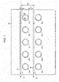
- Fig. 1 illustrates an example of a configuration in which a plurality of general array antennas are disposed.
- the array antenna 10 illustrated in Fig. 1 includes a feed line 30, a plurality of antenna elements 50a through 50n, and an input port 60.
- Fig. 1 illustrates an example in which an array antenna 10' having the same configuration as the array antenna 10 is provided on one surface of a substrate 20 apart by a gap Dp from the array antenna 10.
- the substrate 20 is, for example, a double-sided copper-clad substrate.
- the feed line 30 constitutes a microstrip line with a conductor plate (not illustrated) formed on the other surface of the substrate 20.
- the feed line 30 is linear and formed from a copper foil pattern or the like that has a line width achieving a predetermined characteristic impedance.
- Each of the antenna elements 50a through 50n is a loop-shaped element having a cutout part.
- the antenna elements 50a through 50n are disposed along the feed line 30 at regular gap. More specifically, the antenna elements 50a through 50n are disposed so that the centers of the loop shapes of the antenna elements 50a through 50n are located along the feed line 30 at regular gap.
- Each of the antenna elements 50a through 50n has a width W.
- Each of the antenna elements 50a through 50n is provided away by an gap S' from the feed line 30 and is electromagnetically coupled with the feed line 30.
- the feed line 30 supplies an electric current to the antenna elements 50a through 50n by electromagnetic coupling with the antenna elements 50a through 50n.
- the amount of radiation of each of the antenna elements 50a through 50n is controlled by adjusting the gap S' between each of the antenna elements 50a through 50n and the feed line 30.
- the loop shapes of the antenna elements 50a through 50n are adjusted so that the antenna elements 50a through 50n resonate at a desired frequency.
- a desired frequency is 79 GHz, which is a frequency of a radiated wave
- a radius Rn of an inner periphery of each of the antenna elements 50a through 50n is set to approximately 0.48 mm.
- the array antenna 10 illustrated in Fig. 1 obtains a radiated wave of a desired beam pattern by controlling the amount of radiation through adjustment of the gap S' between the feed line 30 and each of the antenna elements 50a through 50n.
- Fig. 2 is a diagram illustrating a relationship between (i) the gap S' between the feed line 30 and each of the antenna elements 50a through 50n and (ii) the amount of radiation.
- the horizontal axis represents the gap S' between the feed line 30 and each of the antenna elements 50a through 50n
- the vertical axis represents the amount of radiation.
- the amount of radiation becomes smaller as the gap S' becomes larger.
- the amount of radiation is not more than 2%.
- the gap Dp between the feed line 30 and a feed line 30' need be set to an approximately half-wavelength of the wavelength of the radiated wave in order to suppress a grating lobe that occurs due to interference between radio waves radiated by the two array antenna 10 and 10'.
- the half-wavelength is approximately 1.9 mm. That is, in the configuration illustrated in Fig. 1 , when the radiated frequency is 79 GHz, the gap Dp need be set to approximately 1.9 mm.
- the gap Dp need be set to approximately 1.9 mm, and the radius of each of the antenna elements 50a through 50n need be set to approximately 0.48 mm.
- the gap S' between the antenna element 50a and the feed line 30 is set to approximately 0.5 mm in order to adjust the amount of radiation of the antenna element 50a to not more than 2%
- an gap S" between the antenna element 50a and the feed line 30' of the array antenna 10' is 0.24 mm
- the width W of the antenna element is 0.1 mm. That is, in this configuration, coupling between the antenna element 50a and the feed line 30' is stronger than that between the antenna element 50a and the feed line 30 in a case where the amount of radiation of the antenna element 50a is adjusted to not more than 2%.
- the amount of radiation of an antenna element can be adjusted by employing a shape of the antenna element so that the resonant frequency of the antenna element is deviated from a desired frequency. Based on this, the present disclosure was accomplished.
- Embodiment 1 of the present disclosure is described in detail below with reference to the drawings. Note that the embodiments described below are examples, and the present disclosure is not limited to these embodiments.
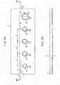
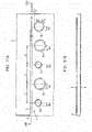
- Figs. 3A and 3B illustrate an example of an array antenna 1 according to Embodiment 1 of the present disclosure.
- Fig. 3A is a plan view of the array antenna 1
- Fig. 3B is a cross-sectional view taken along the line IIIB-IIIB in Fig. 3A .
- the array antenna 1 illustrated in Figs. 3A and 3B includes a substrate 2, a feed line 3, a conductor plate 4, a plurality of antenna elements 5a through 5n, and an input terminal 6.
- the substrate 2 is, for example, a double-sided copper-clad substrate.
- the feed line 3 is formed from a copper foil pattern or the like on one surface of the substrate 2.
- the conductor plate 4 is formed on a surface of the substrate 2 opposite to the surface on which the feed line 3 is formed.
- the conductor plate 4 is ground for the feed line 3 and the antenna elements 5a through 5n.
- the feed line 3 and the conductor plate 4 constitute a microstrip line.
- the input terminal 6 is a feeding point of the array antenna 1. An electric current fed from the input terminal 6 flows through the feed line 3 and Is supplied from the feed line 3 to the antenna elements 5a through 5n.
- the antenna elements 5a through 5n are disposed at regular gap D along the feed line 3 on the surface of the substrate 2 on which the feed line 3 is formed.
- Each of the antenna elements 5a through 5n is a loop-shaped element having a cutout part. More specifically, the antenna elements 5a through 5n are disposed so that the centers of the loop shapes of the antenna elements 5a through 5n are located at the regular gap D along the feed line 3.
- the length of the outer periphery of each of the antenna elements 5a through 5n is approximately 1 wavelength of the resonant frequency thereof. That is, the radius of each of the antenna elements 5a through 5n varies depending on the resonant frequency.
- Each of the antenna elements 5a through 5n has a cutout part having a width G in a circumferential direction of the loop.
- the cutout part is located so that an angle formed by (i) a straight line connecting the center of the antenna element and a substantial center of the cutout part and (ii) the feed line 3 is 45 degrees.
- Each of the antenna elements 5a through 5n is provided away by an gap S from the feed line 3 and is electromagnetically coupled with the feed line 3.
- the feed line 3 supplies an electric current to the antenna elements 5a through 5n by electromagnetic coupling with the antenna elements 5a through 5n.
- the amount of radiation of each of the antenna elements 5a through 5n is controlled by adjusting the gap S between each of the antenna elements 5a through 5n and the feed line 3.
- the radii of the antenna elements 5a through 5n from the centers to the inner peripheries thereof are Ra through Rn.
- a frequency at which each of the antenna elements 50a through 50n resonates is determined by the radius of the loop shape of the antenna element.
- the array antenna 1 radiates a radio wave of a desired beam pattern whose side lobe is suppressed by adjusting the amount of radiation of the antenna elements 5a through 5d located closer to the input terminal 6 to an amount lower than that of the antenna element 5n located farther from the input terminal 6.
- a method for adjusting the amount of radiation of the antenna elements 5a through 5d is described below.
- the shape of the antenna element 5n (hereinafter referred to as a first antenna element) located farther from the input terminal 6 than the antenna element 5d among the antenna elements 5a through 5n is adjusted so that the resonant frequency thereof becomes a frequency (hereinafter referred to as a first frequency) of a radiated wave.
- the shape of each of the antenna elements 5a through 5d (hereinafter referred to as a second antenna element) located closer to the input terminal 6 is adjusted so that the resonant frequency thereof becomes a frequency (hereinafter referred to as a second frequency) that is different by ⁇ f from the first frequency.
- the radius of the second antenna element i.e., the radii Ra through Rd of the antenna elements 5a through 5d
- the radius Rn of the antenna element 5n This causes the second frequency to be higher by ⁇ f (>0) than the first frequency.
- the amount of radiation of the second antenna element is adjusted to a low amount of radiation of not more than 2%.
- the following describes a relationship between the radius Ra of the antenna element 5a as an example of the second antenna element and the amount of radiation.
- Fig. 4 illustrates a relationship between the radius Ra of the antenna element 5a and the resonant frequency of the antenna element 5a.
- the horizontal axis represents the radius Ra
- the vertical axis represents the resonant frequency.
- the resonant frequency of the antenna element 5a can be changed by adjusting the radius Ra of the antenna element 5a.
- Fig. 5 illustrates a relationship between the radius Ra of the antenna element 5a and the amount of radiation of the antenna element 5a.
- the horizontal axis represents the radius Ra as in Fig. 4
- the vertical axis represents the amount of radiation.
- the amount of radiation illustrated in Fig. 5 is the amount of radiation relative to the radius obtained in a case where an electric current for radiation of a radio wave of 79 GHz is fed from the input terminal 6 and the gap S between the feed line 3 and the antenna element 5a is adjusted so that the maximum amount of radiation becomes approximately 7.7%.
- the amount of radiation of the antenna element 5a can be adjusted by adjusting the radius Ra of the antenna element 5a and thereby changing the resonant frequency.
- a low amount of radiation of not more than approximately 2% can be obtained by setting the radius to 0.45 mm or less as illustrated in Fig. 5 .
- the amount of radiation of each of the antenna elements 5b through 5d can be made low by adjusting the radius thereof.
- the amount of radiation of the second antenna element can be adjusted to a low amount of radiation by making the radius of the second antenna element smaller than that of the first antenna element and thereby changing the resonant frequency of the second antenna element.
- the array antenna 1 illustrated in Figs. 3A and 3B can radiate a radio wave of a desired beam pattern whose side lobe is suppressed.
- the antenna elements 5a through 5d have the same shape, but the antenna elements 5a through 5d may have different resonant frequencies, i.e., may have different radii.
- a low amount of radiation of not more than 2% can also be obtained by adjusting the radius to not less than 0.53 mm.
- the following describes an arrangement in which the radius of the second antenna element is made larger.
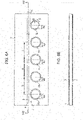
- Figs. 6A and 6B illustrate another example of an array antenna 1' according to Embodiment 1 of the present disclosure.
- Fig. 6A is a plan view of the array antenna 1'
- Fig. 6B is a cross-sectional view taken along the line VIB-VIB in Fig. 6A .
- FIGs. 6A and 6B elements that are identical to those in Figs. 3A and 3B are given identical reference numerals, and detailed description thereof is omitted.
- Antenna elements 5'a through 5'd of the array antenna 1' illustrated in Figs. 6A and 6B are different from the antenna elements 5a through 5d in Fig. 3A
- Each of the antenna elements 5'a through 5'd has a loop shape having a cutout part as with the antenna elements 5a through 5d illustrated in Fig. 3A .
- the antenna elements 5'a through 5'd are located at the same positions as the antenna elements 5a through 5d.
- the radii Ra' through Rd' of the antenna elements 5'a through 5'd are different from the radii Ra through Rd of the antenna elements 5a through 5d,
- Each of the antenna elements 5'a through 5'd is a second antenna element in the array antenna 1'.
- the radius of the second antenna element is larger than that of a first antenna element (a radius Rn of an antenna element 5n). That is, in the configuration illustrated in Figs. 6A and 6B , the second frequency is lower by ⁇ f (> 0) than the first frequency.
- the amount of radiation of the second antenna element can be adjusted to a low amount of radiation by making the radius of the second antenna element larger than that of the first antenna element and thereby changing the resonant frequency of the second antenna element.
- the array antenna 1' illustrated in Figs. 6A and 6B can radiate a radio wave of a desired beam pattern whose side lobe is suppressed.
- Embodiment 1 described above a case where the amount of radiation of an antenna element is adjusted by adjusting the radius of the antenna element and thereby changing the resonant frequency has been described.
- the amount of radiation of an antenna element can also be adjusted by adjusting a size other than the radius of the antenna element and thereby changing the resonant frequency.
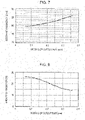
- Fig. 7 illustrates a relationship between a width G of a cutout part of an antenna element (a length in a circumferential direction of a loop) and a resonant frequency of the antenna element.
- the horizontal axis represents the width G of the cutout part of the antenna element
- the vertical axis represents the resonant frequency.
- the resonant frequency of the antenna element can be changed by adjusting the width G of the cutout part of the antenna element.
- Fig. 8 illustrates a relationship between the width G of the cutout part of the antenna element and the amount of radiation of the antenna element.
- the horizontal axis represents the width G of the cutout part of the antenna element as in Fig. 7
- the vertical axis represents the amount of radiation of the antenna element.
- the amount of radiation of the antenna element can be adjusted by adjusting the width G of the cutout part of the antenna element and thereby changing the resonant frequency. Therefore, similar effects can also be obtained by adjustment of the width G of the cutout part of the antenna element instead of adjustment of the radius of the antenna element. Furthermore, it is possible to increase flexibility of design by adjusting not only the radius of the antenna element but also the width G of the cutout part of the antenna element.
- Fig. 9 illustrates a relationship between a width W of an antenna element in a radius direction of the loop and a resonant frequency of the antenna element.
- the horizontal axis represents the width W of the antenna element in a case where the length from the center to the inner periphery (radius) of the antenna element is fixed, and the vertical axis represents the resonant frequency of the antenna element.
- the resonant frequency of the antenna element can be changed by adjusting the width of the antenna element.
- Fig. 10 illustrates a relationship between the width W of the antenna element and the amount of radiation of the antenna element.
- the horizontal axis represents the width W of the antenna element as in Fig. 9
- the vertical axis represents the amount of radiation of the antenna element.
- the amount of radiation of the antenna element can be adjusted by adjusting the width W of the antenna element and thereby changing the resonant frequency. Therefore, similar effects can also be obtained by adjustment of the width W of the antenna element instead of adjustment of the radius of the antenna element or adjustment of the width G of the cutout part of the antenna element. Furthermore, it is possible to increase flexibility of design by adjusting not only the radius of the antenna element and/or the width G of the cutout part of the antenna element, but also the width W of the antenna element.
- the amount of radiation of a loop-shaped antenna element having a cutout part can be adjusted to a low amount of radiation by adjusting the radius of the antenna element, the width of the cutout part in a circumferential direction, or the width of the antenna element in the radius direction and thereby changing the resonant frequency.
- two or more of the radius of the antenna element, the width of the cutout part of the antenna element in the circumferential direction, and the width of the antenna element in the radius direction may be adjusted. Flexibility of design of the antenna element is improved by adjusting two or more of the radius of the antenna element, the width of the cutout part of the antenna element in the circumferential direction, and the width of the antenna element in the radius direction.
- the shape of the antenna element is adjusted so that the resonant frequency thereof becomes a frequency different from a desired frequency in order to obtain a low amount of radiation of not more than approximately 2%. Since the amount of radiation of a radio wave radiated from the antenna element whose shape has been adjusted is low, contribution of the radio wave radiated from the antenna element whose shape has been adjusted to a radio wave radiated from the whole array antenna is small. Accordingly, even in a case where the shape of the antenna element has been adjusted so that the resonant frequency thereof becomes a frequency different from a desired frequency, the influence of the radio wave radiated from the antenna element whose shape has been adjusted on the frequency characteristics of the radio wave radiated from the whole array antenna Is small.
- Embodiment 1 an arrangement in which either an antenna element whose resonant frequency is higher by ⁇ f than a frequency of a radiated wave or an antenna element whose resonant frequency is lower by ⁇ f than the frequency of the radiated wave is provided has been described.
- Embodiment 2 an arrangement in which both of the antenna element whose resonant frequency is higher by ⁇ f than the frequency of the radiated wave and the antenna element whose resonant frequency is lower by ⁇ f than the frequency of the radiated wave are provided Is employed.
- Figs. 11A and 11B are diagrams illustrating an example of a configuration of an array antenna 7 according to Embodiment 2 of the present disclosure.
- Fig. 11A is a plan view of the array antenna 7, and
- Fig. 11B Is a cross-sectional view taken along the line XIB-XIB in Fig. 11A .
- an antenna element that resonates at a second frequency that is higher by ⁇ f than a frequency (first frequency) of a radiated wave is a second antenna element
- an antenna element that resonates at a third frequency that is lower by ⁇ 'f than the frequency (first frequency) of the radiated wave is a third antenna element.
- the first frequency is a frequency between the second frequency and the third frequency
- an absolute value ⁇ f of a difference between the first frequency and the second frequency can be substantially equal to an absolute value ⁇ 'f between the first frequency and the third frequency.
- the antenna elements 5a and 5c whose radii are smaller than a radius Rn of an antenna element 5n are the second antenna element, and the antenna elements 5'b and 5'd whose radii are larger than the radius Rn of the antenna element 5n are the third antenna element.
- the second antenna element and the third antenna element are alternately provided at positions close to the input terminal 6.
- the array antenna 7 illustrated in Figs. 11A and 11B can radiate a radio wave of a desired beam pattern whose side lobe is suppressed as in the array antenna illustrated in Figs. 3A, 3B , 6A and 6B of Embodiment 1.
- the array antenna 7 includes the second antenna element that resonates at a frequency (the second frequency) that is higher by ⁇ f than the frequency (the first frequency) of the radiated wave and the third antenna element that resonates at a frequency (the third frequency) that is lower by ⁇ f than the frequency (the first frequency) of the radiated wave.
- the frequency characteristics of the second antenna element and the frequency characteristics of the third antenna element offset each other. It is therefore possible to further reduce the influence of radio waves radiated from the second antenna element and the third antenna element on the frequency characteristics of radio waves radiated from the whole array antenna.
- the second antenna element and the third antenna element are alternately provided at positions close to the input terminal 6.
- the present embodiment is not limited to this.
- Figs. 12A and 12B illustrate another example of an array antenna 7' according to Embodiment 2 of the present disclosure.
- Fig. 12A is a plan view of the array antenna 7'
- Fig. 12B is a cross-sectional view taken along the line XIIB-XIIB in Fig. 12A .
- the second antenna element and the third antenna element are alternately provided at positions close to the input terminal 6.
- the array antenna 7' illustrated in Figs. 12A and 12B two second antenna elements (antenna elements 5a and 5b) are provided at positions close to the input terminal 6, and two third antenna elements (antenna elements 5'c and 5'd) are provided at positions far from the input terminal 6 than the antenna element 5b.
- the array antenna 7' illustrated in Figs. 12A and 12B can radiate a radio wave of a desired beam pattern whose side lobe is suppressed as in the array antenna 7 illustrated in Figs. 11A and 11B . Furthermore, the array antenna 7' can further reduce the influence of radio waves radiated from the second antenna element and the third antenna element on frequency characteristics of radio waves radiated from the whole array antenna, as in the array antenna 7 Illustrated in Figs. 11A and 11B .
- an antenna element having a cutout part whose width G is large and an antenna element having a cutout part whose width G is small may be disposed as described in Variation 1 of Embodiment 1.
- an antenna element whose width W is large and an antenna element whose width W is small may be disposed as described in Variation 2 of Embodiment 1.
- an antenna element has a loop shape having a cutout part.
- the present disclosure is not limited to this.
- the present disclosure can be applied to an antenna element of any shape provided that the antenna element is electromagnetically coupled with a feed line and the resonant frequency thereof can be adjusted, and thus the amount of radiation of the antenna element can be adjusted.
- An array antenna according to the present disclosure can be used for an on-board radar and the like.
Landscapes
- Physics & Mathematics (AREA)
- Electromagnetism (AREA)
- Variable-Direction Aerials And Aerial Arrays (AREA)
- Waveguide Aerials (AREA)
Applications Claiming Priority (1)
| Application Number | Priority Date | Filing Date | Title |
|---|---|---|---|
| JP2015029660A JP6480751B2 (ja) | 2015-02-18 | 2015-02-18 | アレイアンテナ装置 |
Publications (2)
| Publication Number | Publication Date |
|---|---|
| EP3059802A1 EP3059802A1 (en) | 2016-08-24 |
| EP3059802B1 true EP3059802B1 (en) | 2022-08-03 |
Family
ID=55129691
Family Applications (1)
| Application Number | Title | Priority Date | Filing Date |
|---|---|---|---|
| EP16151165.4A Active EP3059802B1 (en) | 2015-02-18 | 2016-01-14 | Array antenna |
Country Status (4)
| Country | Link |
|---|---|
| US (1) | US9859622B2 (enExample) |
| EP (1) | EP3059802B1 (enExample) |
| JP (1) | JP6480751B2 (enExample) |
| CN (1) | CN105896103A (enExample) |
Families Citing this family (3)
| Publication number | Priority date | Publication date | Assignee | Title |
|---|---|---|---|---|
| JP7593587B2 (ja) * | 2020-09-10 | 2024-12-03 | ミネベアミツミ株式会社 | アンテナ装置、給電装置、及び給電方法 |
| CN114090107A (zh) * | 2021-08-30 | 2022-02-25 | 讯牧信息科技(上海)有限公司 | 计算机和系统启动方法 |
| WO2024174199A1 (zh) * | 2023-02-24 | 2024-08-29 | 京东方科技集团股份有限公司 | 一种毫米波天线、电子设备及其驱动方法 |
Family Cites Families (10)
| Publication number | Priority date | Publication date | Assignee | Title |
|---|---|---|---|---|
| GB2064877B (en) * | 1979-11-22 | 1983-07-27 | Secr Defence | Microstrip antenna |
| JP3306592B2 (ja) | 1999-05-21 | 2002-07-24 | 株式会社豊田中央研究所 | マイクロストリップアレーアンテナ |
| JP2003513496A (ja) * | 1999-10-26 | 2003-04-08 | フラクトゥス・ソシエダッド・アノニマ | インタレースマルチバンドアンテナアレイ |
| ATE279795T1 (de) * | 2000-07-13 | 2004-10-15 | Thomson Licensing Sa | Mehrband-planarantenne |
| US6795020B2 (en) * | 2002-01-24 | 2004-09-21 | Ball Aerospace And Technologies Corp. | Dual band coplanar microstrip interlaced array |
| ES2380580T3 (es) * | 2005-10-14 | 2012-05-16 | Fractus S.A. | Formación menuda de antenas de triple banda para estaciones base celulares |
| JP5091044B2 (ja) * | 2008-07-31 | 2012-12-05 | 株式会社デンソー | マイクロストリップアレーアンテナ |
| DE102010040793A1 (de) * | 2010-09-15 | 2012-03-15 | Robert Bosch Gmbh | Gruppenantenne für Radarsensoren |
| CN103828127B (zh) * | 2012-09-20 | 2015-11-25 | 松下电器产业株式会社 | 阵列天线装置 |
| US9871296B2 (en) * | 2013-06-25 | 2018-01-16 | Huawei Technologies Co., Ltd. | Mixed structure dual-band dual-beam three-column phased array antenna |
-
2015
- 2015-02-18 JP JP2015029660A patent/JP6480751B2/ja active Active
- 2015-12-02 CN CN201510869350.6A patent/CN105896103A/zh active Pending
-
2016
- 2016-01-14 US US14/996,090 patent/US9859622B2/en active Active
- 2016-01-14 EP EP16151165.4A patent/EP3059802B1/en active Active
Also Published As
| Publication number | Publication date |
|---|---|
| US9859622B2 (en) | 2018-01-02 |
| EP3059802A1 (en) | 2016-08-24 |
| CN105896103A (zh) | 2016-08-24 |
| JP6480751B2 (ja) | 2019-03-13 |
| US20160240934A1 (en) | 2016-08-18 |
| JP2016152543A (ja) | 2016-08-22 |
Similar Documents
| Publication | Publication Date | Title |
|---|---|---|
| EP3522297B1 (en) | Wide angle coverage antenna | |
| US9768512B2 (en) | Radar array antenna | |
| EP3264530B1 (en) | Antenna apparatus | |
| EP1748516B1 (en) | Plate board type mimo array antenna including isolation element | |
| US8736507B2 (en) | Antenna apparatus provided with dipole antenna and parasitic element pairs as arranged at intervals | |
| JP6395984B2 (ja) | アレーアンテナ装置 | |
| US10020594B2 (en) | Array antenna | |
| US8742990B2 (en) | Circular polarization antenna | |
| US20140078005A1 (en) | Radar array antenna using open stubs | |
| US8736514B2 (en) | Antenna | |
| JP2007081825A (ja) | 漏れ波アンテナ | |
| EP3062394B1 (en) | Array antenna device | |
| US10756446B2 (en) | Planar antenna structure with reduced coupling between antenna arrays | |
| US20100271277A1 (en) | Slot Antenna | |
| US20240313399A1 (en) | Antenna unit and multi-beam antenna | |
| EP3059802B1 (en) | Array antenna | |
| KR101803208B1 (ko) | 단일 방사체 다중 급전을 이용한 빔조향 안테나 | |
| JP2016086432A (ja) | アレーアンテナおよびレーダ装置 | |
| KR101865135B1 (ko) | 배열 안테나 | |
| JP2013135345A (ja) | マイクロストリップアンテナ、アレーアンテナおよびレーダ装置 | |
| EP3312934B1 (en) | Antenna | |
| US10361475B2 (en) | Antenna unit and antenna system | |
| US10516211B2 (en) | Dual band antenna | |
| KR102039398B1 (ko) | 복수의 주파수 대역에서 동작하는 통합 안테나 | |
| KR101974156B1 (ko) | 송신 배열 안테나 장치, 이를 구비하는 무선 전력 전송 시스템 및 그의 역지향성 빔포밍 방법 |
Legal Events
| Date | Code | Title | Description |
|---|---|---|---|
| PUAI | Public reference made under article 153(3) epc to a published international application that has entered the european phase |
Free format text: ORIGINAL CODE: 0009012 |
|
| AK | Designated contracting states |
Kind code of ref document: A1 Designated state(s): AL AT BE BG CH CY CZ DE DK EE ES FI FR GB GR HR HU IE IS IT LI LT LU LV MC MK MT NL NO PL PT RO RS SE SI SK SM TR |
|
| AX | Request for extension of the european patent |
Extension state: BA ME |
|
| STAA | Information on the status of an ep patent application or granted ep patent |
Free format text: STATUS: REQUEST FOR EXAMINATION WAS MADE |
|
| 17P | Request for examination filed |
Effective date: 20170222 |
|
| RBV | Designated contracting states (corrected) |
Designated state(s): AL AT BE BG CH CY CZ DE DK EE ES FI FR GB GR HR HU IE IS IT LI LT LU LV MC MK MT NL NO PL PT RO RS SE SI SK SM TR |
|
| STAA | Information on the status of an ep patent application or granted ep patent |
Free format text: STATUS: EXAMINATION IS IN PROGRESS |
|
| 17Q | First examination report despatched |
Effective date: 20201113 |
|
| GRAP | Despatch of communication of intention to grant a patent |
Free format text: ORIGINAL CODE: EPIDOSNIGR1 |
|
| STAA | Information on the status of an ep patent application or granted ep patent |
Free format text: STATUS: GRANT OF PATENT IS INTENDED |
|
| INTG | Intention to grant announced |
Effective date: 20220225 |
|
| RAP3 | Party data changed (applicant data changed or rights of an application transferred) |
Owner name: PANASONIC HOLDINGS CORPORATION |
|
| GRAS | Grant fee paid |
Free format text: ORIGINAL CODE: EPIDOSNIGR3 |
|
| GRAA | (expected) grant |
Free format text: ORIGINAL CODE: 0009210 |
|
| STAA | Information on the status of an ep patent application or granted ep patent |
Free format text: STATUS: THE PATENT HAS BEEN GRANTED |
|
| AK | Designated contracting states |
Kind code of ref document: B1 Designated state(s): AL AT BE BG CH CY CZ DE DK EE ES FI FR GB GR HR HU IE IS IT LI LT LU LV MC MK MT NL NO PL PT RO RS SE SI SK SM TR |
|
| REG | Reference to a national code |
Ref country code: AT Ref legal event code: REF Ref document number: 1509497 Country of ref document: AT Kind code of ref document: T Effective date: 20220815 Ref country code: CH Ref legal event code: EP |
|
| REG | Reference to a national code |
Ref country code: DE Ref legal event code: R096 Ref document number: 602016073896 Country of ref document: DE |
|
| REG | Reference to a national code |
Ref country code: IE Ref legal event code: FG4D |
|
| REG | Reference to a national code |
Ref country code: LT Ref legal event code: MG9D |
|
| REG | Reference to a national code |
Ref country code: NL Ref legal event code: MP Effective date: 20220803 |
|
| PG25 | Lapsed in a contracting state [announced via postgrant information from national office to epo] |
Ref country code: SE Free format text: LAPSE BECAUSE OF FAILURE TO SUBMIT A TRANSLATION OF THE DESCRIPTION OR TO PAY THE FEE WITHIN THE PRESCRIBED TIME-LIMIT Effective date: 20220803 Ref country code: RS Free format text: LAPSE BECAUSE OF FAILURE TO SUBMIT A TRANSLATION OF THE DESCRIPTION OR TO PAY THE FEE WITHIN THE PRESCRIBED TIME-LIMIT Effective date: 20220803 Ref country code: PT Free format text: LAPSE BECAUSE OF FAILURE TO SUBMIT A TRANSLATION OF THE DESCRIPTION OR TO PAY THE FEE WITHIN THE PRESCRIBED TIME-LIMIT Effective date: 20221205 Ref country code: NO Free format text: LAPSE BECAUSE OF FAILURE TO SUBMIT A TRANSLATION OF THE DESCRIPTION OR TO PAY THE FEE WITHIN THE PRESCRIBED TIME-LIMIT Effective date: 20221103 Ref country code: NL Free format text: LAPSE BECAUSE OF FAILURE TO SUBMIT A TRANSLATION OF THE DESCRIPTION OR TO PAY THE FEE WITHIN THE PRESCRIBED TIME-LIMIT Effective date: 20220803 Ref country code: LV Free format text: LAPSE BECAUSE OF FAILURE TO SUBMIT A TRANSLATION OF THE DESCRIPTION OR TO PAY THE FEE WITHIN THE PRESCRIBED TIME-LIMIT Effective date: 20220803 Ref country code: LT Free format text: LAPSE BECAUSE OF FAILURE TO SUBMIT A TRANSLATION OF THE DESCRIPTION OR TO PAY THE FEE WITHIN THE PRESCRIBED TIME-LIMIT Effective date: 20220803 Ref country code: FI Free format text: LAPSE BECAUSE OF FAILURE TO SUBMIT A TRANSLATION OF THE DESCRIPTION OR TO PAY THE FEE WITHIN THE PRESCRIBED TIME-LIMIT Effective date: 20220803 Ref country code: ES Free format text: LAPSE BECAUSE OF FAILURE TO SUBMIT A TRANSLATION OF THE DESCRIPTION OR TO PAY THE FEE WITHIN THE PRESCRIBED TIME-LIMIT Effective date: 20220803 |
|
| REG | Reference to a national code |
Ref country code: AT Ref legal event code: MK05 Ref document number: 1509497 Country of ref document: AT Kind code of ref document: T Effective date: 20220803 |
|
| PG25 | Lapsed in a contracting state [announced via postgrant information from national office to epo] |
Ref country code: PL Free format text: LAPSE BECAUSE OF FAILURE TO SUBMIT A TRANSLATION OF THE DESCRIPTION OR TO PAY THE FEE WITHIN THE PRESCRIBED TIME-LIMIT Effective date: 20220803 Ref country code: IS Free format text: LAPSE BECAUSE OF FAILURE TO SUBMIT A TRANSLATION OF THE DESCRIPTION OR TO PAY THE FEE WITHIN THE PRESCRIBED TIME-LIMIT Effective date: 20221203 Ref country code: HR Free format text: LAPSE BECAUSE OF FAILURE TO SUBMIT A TRANSLATION OF THE DESCRIPTION OR TO PAY THE FEE WITHIN THE PRESCRIBED TIME-LIMIT Effective date: 20220803 Ref country code: GR Free format text: LAPSE BECAUSE OF FAILURE TO SUBMIT A TRANSLATION OF THE DESCRIPTION OR TO PAY THE FEE WITHIN THE PRESCRIBED TIME-LIMIT Effective date: 20221104 |
|
| PG25 | Lapsed in a contracting state [announced via postgrant information from national office to epo] |
Ref country code: SM Free format text: LAPSE BECAUSE OF FAILURE TO SUBMIT A TRANSLATION OF THE DESCRIPTION OR TO PAY THE FEE WITHIN THE PRESCRIBED TIME-LIMIT Effective date: 20220803 Ref country code: RO Free format text: LAPSE BECAUSE OF FAILURE TO SUBMIT A TRANSLATION OF THE DESCRIPTION OR TO PAY THE FEE WITHIN THE PRESCRIBED TIME-LIMIT Effective date: 20220803 Ref country code: DK Free format text: LAPSE BECAUSE OF FAILURE TO SUBMIT A TRANSLATION OF THE DESCRIPTION OR TO PAY THE FEE WITHIN THE PRESCRIBED TIME-LIMIT Effective date: 20220803 Ref country code: CZ Free format text: LAPSE BECAUSE OF FAILURE TO SUBMIT A TRANSLATION OF THE DESCRIPTION OR TO PAY THE FEE WITHIN THE PRESCRIBED TIME-LIMIT Effective date: 20220803 Ref country code: AT Free format text: LAPSE BECAUSE OF FAILURE TO SUBMIT A TRANSLATION OF THE DESCRIPTION OR TO PAY THE FEE WITHIN THE PRESCRIBED TIME-LIMIT Effective date: 20220803 |
|
| REG | Reference to a national code |
Ref country code: DE Ref legal event code: R097 Ref document number: 602016073896 Country of ref document: DE |
|
| PG25 | Lapsed in a contracting state [announced via postgrant information from national office to epo] |
Ref country code: SK Free format text: LAPSE BECAUSE OF FAILURE TO SUBMIT A TRANSLATION OF THE DESCRIPTION OR TO PAY THE FEE WITHIN THE PRESCRIBED TIME-LIMIT Effective date: 20220803 Ref country code: EE Free format text: LAPSE BECAUSE OF FAILURE TO SUBMIT A TRANSLATION OF THE DESCRIPTION OR TO PAY THE FEE WITHIN THE PRESCRIBED TIME-LIMIT Effective date: 20220803 |
|
| PLBE | No opposition filed within time limit |
Free format text: ORIGINAL CODE: 0009261 |
|
| STAA | Information on the status of an ep patent application or granted ep patent |
Free format text: STATUS: NO OPPOSITION FILED WITHIN TIME LIMIT |
|
| PG25 | Lapsed in a contracting state [announced via postgrant information from national office to epo] |
Ref country code: AL Free format text: LAPSE BECAUSE OF FAILURE TO SUBMIT A TRANSLATION OF THE DESCRIPTION OR TO PAY THE FEE WITHIN THE PRESCRIBED TIME-LIMIT Effective date: 20220803 |
|
| 26N | No opposition filed |
Effective date: 20230504 |
|
| PG25 | Lapsed in a contracting state [announced via postgrant information from national office to epo] |
Ref country code: SI Free format text: LAPSE BECAUSE OF FAILURE TO SUBMIT A TRANSLATION OF THE DESCRIPTION OR TO PAY THE FEE WITHIN THE PRESCRIBED TIME-LIMIT Effective date: 20220803 |
|
| REG | Reference to a national code |
Ref country code: CH Ref legal event code: PL |
|
| GBPC | Gb: european patent ceased through non-payment of renewal fee |
Effective date: 20230114 |
|
| PG25 | Lapsed in a contracting state [announced via postgrant information from national office to epo] |
Ref country code: LU Free format text: LAPSE BECAUSE OF NON-PAYMENT OF DUE FEES Effective date: 20230114 |
|
| REG | Reference to a national code |
Ref country code: BE Ref legal event code: MM Effective date: 20230131 |
|
| PG25 | Lapsed in a contracting state [announced via postgrant information from national office to epo] |
Ref country code: LI Free format text: LAPSE BECAUSE OF NON-PAYMENT OF DUE FEES Effective date: 20230131 Ref country code: GB Free format text: LAPSE BECAUSE OF NON-PAYMENT OF DUE FEES Effective date: 20230114 Ref country code: CH Free format text: LAPSE BECAUSE OF NON-PAYMENT OF DUE FEES Effective date: 20230131 |
|
| PG25 | Lapsed in a contracting state [announced via postgrant information from national office to epo] |
Ref country code: FR Free format text: LAPSE BECAUSE OF NON-PAYMENT OF DUE FEES Effective date: 20230131 Ref country code: BE Free format text: LAPSE BECAUSE OF NON-PAYMENT OF DUE FEES Effective date: 20230131 |
|
| PG25 | Lapsed in a contracting state [announced via postgrant information from national office to epo] |
Ref country code: IE Free format text: LAPSE BECAUSE OF NON-PAYMENT OF DUE FEES Effective date: 20230114 |
|
| REG | Reference to a national code |
Ref country code: DE Ref legal event code: R081 Ref document number: 602016073896 Country of ref document: DE Owner name: PANASONIC AUTOMOTIVE SYSTEMS CO., LTD., YOKOHA, JP Free format text: FORMER OWNER: PANASONIC HOLDINGS CORPORATION, OSAKA, JP |
|
| PG25 | Lapsed in a contracting state [announced via postgrant information from national office to epo] |
Ref country code: IT Free format text: LAPSE BECAUSE OF FAILURE TO SUBMIT A TRANSLATION OF THE DESCRIPTION OR TO PAY THE FEE WITHIN THE PRESCRIBED TIME-LIMIT Effective date: 20220803 |
|
| PG25 | Lapsed in a contracting state [announced via postgrant information from national office to epo] |
Ref country code: MC Free format text: LAPSE BECAUSE OF FAILURE TO SUBMIT A TRANSLATION OF THE DESCRIPTION OR TO PAY THE FEE WITHIN THE PRESCRIBED TIME-LIMIT Effective date: 20220803 |
|
| PG25 | Lapsed in a contracting state [announced via postgrant information from national office to epo] |
Ref country code: MC Free format text: LAPSE BECAUSE OF FAILURE TO SUBMIT A TRANSLATION OF THE DESCRIPTION OR TO PAY THE FEE WITHIN THE PRESCRIBED TIME-LIMIT Effective date: 20220803 |
|
| PG25 | Lapsed in a contracting state [announced via postgrant information from national office to epo] |
Ref country code: BG Free format text: LAPSE BECAUSE OF FAILURE TO SUBMIT A TRANSLATION OF THE DESCRIPTION OR TO PAY THE FEE WITHIN THE PRESCRIBED TIME-LIMIT Effective date: 20220803 |
|
| PG25 | Lapsed in a contracting state [announced via postgrant information from national office to epo] |
Ref country code: BG Free format text: LAPSE BECAUSE OF FAILURE TO SUBMIT A TRANSLATION OF THE DESCRIPTION OR TO PAY THE FEE WITHIN THE PRESCRIBED TIME-LIMIT Effective date: 20220803 |
|
| PGFP | Annual fee paid to national office [announced via postgrant information from national office to epo] |
Ref country code: DE Payment date: 20250121 Year of fee payment: 10 |
|
| PG25 | Lapsed in a contracting state [announced via postgrant information from national office to epo] |
Ref country code: CY Free format text: LAPSE BECAUSE OF FAILURE TO SUBMIT A TRANSLATION OF THE DESCRIPTION OR TO PAY THE FEE WITHIN THE PRESCRIBED TIME-LIMIT; INVALID AB INITIO Effective date: 20160114 |
|
| PG25 | Lapsed in a contracting state [announced via postgrant information from national office to epo] |
Ref country code: HU Free format text: LAPSE BECAUSE OF FAILURE TO SUBMIT A TRANSLATION OF THE DESCRIPTION OR TO PAY THE FEE WITHIN THE PRESCRIBED TIME-LIMIT; INVALID AB INITIO Effective date: 20160114 |