EP3059711A1 - Coin identification device - Google Patents
Coin identification device Download PDFInfo
- Publication number
- EP3059711A1 EP3059711A1 EP14854387.9A EP14854387A EP3059711A1 EP 3059711 A1 EP3059711 A1 EP 3059711A1 EP 14854387 A EP14854387 A EP 14854387A EP 3059711 A1 EP3059711 A1 EP 3059711A1
- Authority
- EP
- European Patent Office
- Prior art keywords
- coin
- identification sensor
- plated
- identification
- processing device
- Prior art date
- Legal status (The legal status is an assumption and is not a legal conclusion. Google has not performed a legal analysis and makes no representation as to the accuracy of the status listed.)
- Granted
Links
Images




Classifications
-
- G—PHYSICS
- G07—CHECKING-DEVICES
- G07D—HANDLING OF COINS OR VALUABLE PAPERS, e.g. TESTING, SORTING BY DENOMINATIONS, COUNTING, DISPENSING, CHANGING OR DEPOSITING
- G07D5/00—Testing specially adapted to determine the identity or genuineness of coins, e.g. for segregating coins which are unacceptable or alien to a currency
- G07D5/08—Testing the magnetic or electric properties
-
- G—PHYSICS
- G07—CHECKING-DEVICES
- G07D—HANDLING OF COINS OR VALUABLE PAPERS, e.g. TESTING, SORTING BY DENOMINATIONS, COUNTING, DISPENSING, CHANGING OR DEPOSITING
- G07D5/00—Testing specially adapted to determine the identity or genuineness of coins, e.g. for segregating coins which are unacceptable or alien to a currency
Definitions
- the present invention relates to a coin processing device, in particular to a coin processing device for identifying plated coins.
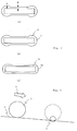
- the plated coins include coins obtained by performing nickel plating on iron, for example, and wear resistance and corrosion resistance of the coins are improved. Therefore, as shown in Fig.1(b) which is a cross section figure of the straight line X-X' in the drawing of the coin 501 shown in Fig. 1 (a) , the coin 501 is constituted by two materials, namely iron 502 and nickel 503.
- an identification sensor 505 and an identification sensor 506 are arranged in a coin passage 504 inclined so that the coin 501 rotatively moves in the direction of the arrow Y in the drawing, and the identification sensor 505 identifies a core material of the coin and the identification sensor 506 identifies a plated material of the coin surface layer.
- the identification sensors 505, 506 are both coils connected to an oscillation circuit, and the identification sensor 505 is oscillated at relatively low frequency (40 kHz, for example) and the identification sensor 506 is oscillated at relatively high frequency (500 kHz, for example), thereby can identify the core material and the plated material of the coin respectively.
- Patent document 1 Japanese Patent No. 4126668
- the plating on the coin surface layer of the plated coin is about several ⁇ m to several tens ⁇ m thick, being sometimes inconsistent, and thus, it was difficult to grasp the characteristics of the plated coin with high accuracy. Accordingly, genuine plated coins and forged plated coins could not always be distinguished with high accuracy.
- the present invention has the purpose of providing the coin processing device capable of identifying a plated coin with high accuracy.
- the invention in claim 1 is characterized with a coin identification device which identifies a plated coin characterized by comprising an identification sensor formed of coils arranged on a wall face of a coin passage in which the coin rotatively moves, in a position where a thickly plated part of layer of the coin passes through, and determination means for determining coin genuineness by obtaining from output of the identification sensor characteristic data including characteristics of both of a plated layer and a core material of the coin.
- the invention in claim 2 is characterized, in the invention in claim 1, in that the identification sensor is arranged on an upper part and a lower part of the wall face of the coin passage.
- the invention in claim 3 is characterized, in the invention in claim 2, in that the identification sensor is arc-shaped according to diameter of the coin to be identified.
- the invention in claim 4 is characterized, in the invention in claim 1, in that the identification sensor is annularly shaped with circumference according to the diameter of the coin to be identified.
- the invention in claim 5 is characterized, in any of the inventions in claims 1-4, in that the identification sensor comprises printed coils obtained by forming a spiral coil of metal foil on a substrate.
- a plated coin can be identified with high precision by making use of its characteristics.
- the present invention intends to determine genuineness of coins while paying attention to the dog-bone effect generated when a coin is plated.
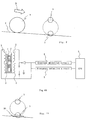
- Fig. 3 explains the dog-bone effect.
- Fig. 3 (a) and Fig. 3 (b) show a genuine coin constituted by a core material 11 and a plated layer 12.
- Fig. 3 (c) shows a forged coin constituted by a core material 13 and a plated layer 14.
- Plating by electroplating concentrates electrical field to the edge of the core material making the plated layer in the edge thicker than the other plated area.
- B defined as the thickness of the plated layer around the center of the coin is smaller than A defined as the thickness of the plated layer in the margin of the coin which is the edge of the core material, namely shown as A>B.
- the plated layer in the margin of the coin namely the edge of the core material thicker than the plated layer in the center of the coin allows the characteristics of the plate material to be obtained more easily.
- the investigation of the actual genuine/forged coin has confirmed that, due to the difference of plating effect between a genuine coin and a forged coin, the thickness of the plated layer in the margin of the genuine coin due to the dog-bone effect is different from the thickness of the plated layer in the margin of the forged coin due to the dog-bone effect, as shown in the genuine coin in Fig. 3 (b) and the forged coin in Fig. 3 (c) .
- the thickness of the plated layer in the margin of the coin is recognized as characteristic, and this characteristic is utilized to determine the genuineness of the coin.
- Fig. 4 shows an example of how the identification sensor in the coin processing device in Embodiment 1 in the present invention is arranged.
- the identification sensor 3 is arranged in the coin passage 2 inclined so that the coin 1 rotatively moves in the direction of the arrow C in the drawing.
- This identification sensor 3 is arranged in the lower part in the coin passage 2, where the part of the layer in the coin 1 thickly plated due to the dog-bone effect passes through.
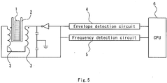
- the identification sensor 3 comprises a pair of coils and, as shown in Fig. 5 , is connected to an oscillation circuit in series and oscillates at 500 kHz.
- CPU 6 obtains voltage from the oscillation circuit by way of an envelope detection circuit 4, obtains frequency by way of a frequency detection circuit 5.
- the CPU 6 functions as determination means, and determines the genuineness of the coin by using determination function to the obtained voltage and frequency.
- a method for determining the genuineness of coins from the obtained voltage value and frequency value by using the determination function such a method as the method for determination based on whether or not the obtained value of voltage or frequency is included within the range of predetermined threshold value and the method for comprehensive determination based on how similar the obtained values of both of voltage and frequency and the genuine coin data prestored in a memory, etc. are to each other can be used, for example.
- a winding coil obtained by winding copper wire, etc. around a core or a printed coil obtained by spirally printing metal foil on a substrate can be used.
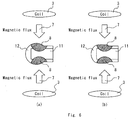
- Fig. 6 explains the principle for determining coins.
- the magnetic flux 7 generated in the identification sensor (coils) 3 causes eddy current to be generated in the coin, and this eddy current causes the voltage and its frequency output from the identification sensor 3 to be changed.
- the voltage and its frequency output from the identification sensor 3 change differently in comparison between the case where the genuine coin has passed and the case where the forged coin has passed, and the difference enables the genuine coin and the forged coin to be determined.
- the characteristic data of the coin composed of the voltage value and frequency value obtained from the coin includes characteristics of both of the plated layer and the core material in the thickly plated part of the layer. Therefore, in the coin processing device in Embodiment 1 in the present invention, the genuineness is determined based on the characteristic data including the characteristics of both of the plated layer and the core material.
- the identification sensor 3 is arranged in the thickly plated position of the layer, and the sensor oscillates at relatively high frequency, and thus, the voltage value and frequency value obtained in the coils 3 notably reflect the difference of plated layer thickness between the genuine coin and the forged coin, and thereby the plated coin can be identified with high precision.
- the identification sensor 3 oscillates at 500 kHz, this frequency is not limited as long as it is subject to the characteristics of the coin surface layer, which is the frequency from 200 kHz to 600 kHz.
- Fig. 7 shows the flow of operation of the coin processing device.
- the coin processing device When the coin processing device starts its operation, it waits for the coin 1 to be thrown.
- the coin 1 When the coin 1 is thrown, rotatively moves in the coin passage 2 and reaches the vicinity of the identification sensor 3, the output (voltage and its frequency) of the identification sensor 3 changes.
- the voltage of the identification sensor 3 changes as shown in Fig. 8 , for example, with t1 representing the time when the coin 1 has reached the vicinity of the identification sensor 3. It is noted that the identification sensor 3 detects the coin 1 between the time t1 and the time t3.
- CPU 6 obtains voltage by way of an envelope detection circuit 4, obtains frequency by way of a frequency detection circuit 5, and stores them in a memory not shown (Step 102).
- the voltage and frequency are regularly obtained and stored (Step 102) until the coin 1 has passed through around the center of the identification sensor 3 (NO in Step 103). It is noted that the CPU 6 determines from the output of the identification sensor 3 whether or not the coin 1 has passed through around the center of the identification sensor 3. When the coin 1 has passed through around the center of the identification sensor 3, the voltage of the identification sensor 3 which has been decreasing begins to increase as the time t2 shows in Fig. 8 , and thus, this output change is recognized as indicating that the coin 1 has passed through around the center of the identification sensor 3.
- the CPU 6 When the coin 1 has passed through around the center of the identification sensor 3 (YES in Step 103), the CPU 6 performs a calculation by substituting the voltage and frequency at the time when the coin 1 has passed through around the center of the identification sensor 3 into the predetermined determination function (Step 104), determines the genuineness of the passing coin 1 based on the calculation result (Step 105), and finishes the processing.
- Embodiment 1 an explanation of how a coin is identified by the use of a pair of identification sensors 3 is shown, whereas in Embodiment 2, an explanation of how a coin is identified by the use of two pairs of identification sensors is shown.
- Fig. 9 shows an example of how the identification sensor in the coin processing device in Embodiment 2 in the present invention is arranged.
- the identification sensor 3 is arranged in the coin passage 2, inclined so that the coin 1 rotatively moves in the direction of the arrow D in the drawing.
- This identification sensor 3 is arranged in the lower part and the upper part in the coin passage 2, where the part of the layer in the coin 1 thickly plated due to the dog-bone effect passes through.
- the identification sensor 3 arranged in the upper part in the coin passage 2 is arranged in the part upper from the floor face of the coin passage 2 to the same extent as the diameter of the coin 1.
- the identification sensor 3 comprises two pairs of coils and, as shown in Fig. 10 , is connected to an oscillation circuit, obtains voltage from the oscillation circuit by way of an envelope detection circuit 4, obtains frequency by way of a frequency detection circuit 5, inputs the obtained voltage and frequency respectively to CPU 6, and uses determination function, in order to determine the genuineness of the coin.
- a winding coil obtained by winding copper wire, etc. around a core or a printed coil obtained by spirally printing metal foil on a substrate can be used.
- Embodiment 3 the identification sensor with a coil having a shape different from the shape of the coils used in Embodiment 1 and Embodiment 2 is explained.
- Fig. 12 shows an example of how the identification sensor in the coin processing device in Embodiment 3 in the present invention is arranged.
- the identification sensor 203 is arranged in the coin passage 2 inclined so that the coin 1 rotatively moves in the direction of the arrow E in the drawing.
- This identification sensor 203 is arranged in the coin passage 2 in the position where the part of the layer in the coin 1 thickly plated due to the dock-bone effect passes through, so that the above part can be entirely detected.
- the above identification sensor 203 is an annular printed coil as shown in Fig. 13 . Since this identification sensor 203 has no coil at the center, and a printed coil has smaller inductance and weaker magnetic field than a winding coil, the magnetic flux diffuses less from the center of the printed coil in comparison with the case of the winding coil. Thereby, the identification sensor 203 is free from any influence from the center of the coin, and the characteristics (voltage value and frequency value) of the edge of the coin can be obtained with high precision.
- the identification sensor 203 entirely detects the part of the layer in the coin 1 thickly plated due to the dog-bone effect, such a case as coin variance or accumulation of dust, etc. in the coin passage 2 would not inhibit the genuineness of the coin 1 from being determined with relatively high precision.
- circuit configuration in the coin processing device in Embodiment 3 is the same as the circuit configuration ( Fig. 5 ) in the coin processing device in Embodiment 1. Also, the principle for determining coins and the operation of the coin processing device are not explained here, since they are the same as in Embodiment 1.
- Embodiment 4 the identification sensor with a coil having a shape different from the shape of the coils used in Embodiment 1, Embodiment 2 and Embodiment 3 is explained.
- Fig. 14 shows an example of how the identification sensor in the coin processing device in Embodiment 4 in the present invention is arranged.
- the identification sensor 303 is arranged in the coin passage 2 inclined so that the coin 1 rotatively moves in the direction of the arrow F in the drawing.
- This identification sensor 203 is arranged in the lower part and the upper part in the coin passage 2, where the part of the layer in the coin 1 thickly plated due to the dog-bone effect passes through.
- the identification sensor 3 arranged in the upper part in the coin passage 2 is arranged in the part upper from the floor face of the coin passage 2 to the same extent as the diameter of the coin 1.
- the identification sensor 303 comprises two pairs of coils, and a winding coil obtained by winding copper wire, etc. around a core or a printed coil obtained by spirally printing metal foil on a substrate can be used.
- the parts in contact with the coin passage 2, namely the faces opposing the coin 1 are arc (bow)-shaped, as shown in Fig. 15 , according to the diameter of the coin 1 to be detected.
- the shape of the coils of the identification sensor 303 is more complicated than in Embodiment 2, but the coin can be determined with higher precision than in Embodiment 2.
- circuit configuration in the coin processing device in Embodiment 4 is the same as the circuit configuration ( Fig. 10 ) in the coin processing device in Embodiment 2. Also, the principle for determining coins and the operation of the coin processing device are not explained here, since they are the same as in Embodiment 1.
Landscapes
- Physics & Mathematics (AREA)
- General Physics & Mathematics (AREA)
- Testing Of Coins (AREA)
- Control Of Vending Devices And Auxiliary Devices For Vending Devices (AREA)
Abstract
Description
- The present invention relates to a coin processing device, in particular to a coin processing device for identifying plated coins.
- Recently, more and more plated foreign coins have been used. The plated coins include coins obtained by performing nickel plating on iron, for example, and wear resistance and corrosion resistance of the coins are improved. Therefore, as shown in
Fig.1(b) which is a cross section figure of the straight line X-X' in the drawing of thecoin 501 shown inFig. 1 (a) , thecoin 501 is constituted by two materials, namelyiron 502 andnickel 503. - When denomination or genuineness of the
coin 501 is identified in a conventional coin processing device as shown inFig. 2 , for example, anidentification sensor 505 and anidentification sensor 506 are arranged in acoin passage 504 inclined so that thecoin 501 rotatively moves in the direction of the arrow Y in the drawing, and theidentification sensor 505 identifies a core material of the coin and theidentification sensor 506 identifies a plated material of the coin surface layer. - The
identification sensors identification sensor 505 is oscillated at relatively low frequency (40 kHz, for example) and theidentification sensor 506 is oscillated at relatively high frequency (500 kHz, for example), thereby can identify the core material and the plated material of the coin respectively. - It is noted that a method for identifying a coin constituted by two different materials is described in the
Patent document 1, for example. - Patent document 1 : Japanese Patent No.
4126668 - However, the plating on the coin surface layer of the plated coin is about several µm to several tens µm thick, being sometimes inconsistent, and thus, it was difficult to grasp the characteristics of the plated coin with high accuracy. Accordingly, genuine plated coins and forged plated coins could not always be distinguished with high accuracy.
- Accordingly, the present invention has the purpose of providing the coin processing device capable of identifying a plated coin with high accuracy.
- In order to achieve the above purpose, the invention in
claim 1 is characterized with a coin identification device which identifies a plated coin characterized by comprising an identification sensor formed of coils arranged on a wall face of a coin passage in which the coin rotatively moves, in a position where a thickly plated part of layer of the coin passes through, and determination means for determining coin genuineness by obtaining from output of the identification sensor characteristic data including characteristics of both of a plated layer and a core material of the coin. - Also, the invention in
claim 2 is characterized, in the invention inclaim 1, in that the identification sensor is arranged on an upper part and a lower part of the wall face of the coin passage. - Also, the invention in
claim 3 is characterized, in the invention inclaim 2, in that the identification sensor is arc-shaped according to diameter of the coin to be identified. - Also, the invention in
claim 4 is characterized, in the invention inclaim 1, in that the identification sensor is annularly shaped with circumference according to the diameter of the coin to be identified. - Also, the invention in
claim 5 is characterized, in any of the inventions in claims 1-4, in that the identification sensor comprises printed coils obtained by forming a spiral coil of metal foil on a substrate. - According the present invention, a plated coin can be identified with high precision by making use of its characteristics.
-
- [
Fig. 1 ] explains a plated coin. - [
Fig. 2 ] shows an example of conventional coin identification device for identifying a plated coin. - [
Fig. 3 ] explains the dog-bone effect. - [
Fig. 4 ] shows an example of how the identification sensor in the coin processing device inEmbodiment 1 in the present invention is arranged. - [
Fig. 5 ] shows a circuit configuration example of the coin processing device inEmbodiment 1 in the present invention. - [
Fig. 6 ] explains the principle for determining coins inEmbodiment 1 in the present invention. - [
Fig. 7 ] shows the flow of operation of the coin processing device inEmbodiment 1 in the present invention. - [
Fig. 8 ] shows an output example of theidentification sensor 3 inEmbodiment 1 in the present invention. - [
Fig. 9 ] shows an example of how the identification sensor in the coin processing device inEmbodiment 2 in the present invention is arranged. - [
Fig. 10 ] shows a circuit configuration example of the coin processing device inEmbodiment 2 in the present invention. - [
Fig. 11 ] explains an example in whichdust 20, etc. is accumulated on the floor face of thecoin passage 2 inEmbodiment 2 in the present invention. - [
Fig. 12 ] shows an example of how the identification sensor in the coin processing device inEmbodiment 3 in the present invention is arranged. - [
Fig. 13 ] shows a configuration example of thecoin identification sensor 203. - [
Fig. 14 ] shows an example of how the identification sensor in the coin processing device inEmbodiment 3 in the present invention is arranged. - [
Fig. 15 ] shows a configuration example of thecoin identification sensor 303. - Shown below is the detailed explanation regarding one embodiment of the coin processing device in the present invention referring to the attached drawings.
- At first, the summary of the invention is explained. The present invention intends to determine genuineness of coins while paying attention to the dog-bone effect generated when a coin is plated.
-
Fig. 3 explains the dog-bone effect.Fig. 3 (a) and Fig. 3 (b) show a genuine coin constituted by acore material 11 and aplated layer 12.Fig. 3 (c) shows a forged coin constituted by acore material 13 and aplated layer 14. Plating by electroplating concentrates electrical field to the edge of the core material making the plated layer in the edge thicker than the other plated area. Thereby, in the plated coin, as shown inFig. 3 (a) , B defined as the thickness of the plated layer around the center of the coin is smaller than A defined as the thickness of the plated layer in the margin of the coin which is the edge of the core material, namely shown as A>B. - Therefore, the plated layer in the margin of the coin, namely the edge of the core material thicker than the plated layer in the center of the coin allows the characteristics of the plate material to be obtained more easily.
- Also the investigation of the actual genuine/forged coin has confirmed that, due to the difference of plating effect between a genuine coin and a forged coin, the thickness of the plated layer in the margin of the genuine coin due to the dog-bone effect is different from the thickness of the plated layer in the margin of the forged coin due to the dog-bone effect, as shown in the genuine coin in
Fig. 3 (b) and the forged coin inFig. 3 (c) . - In the present invention, the thickness of the plated layer in the margin of the coin is recognized as characteristic, and this characteristic is utilized to determine the genuineness of the coin.
-
Fig. 4 shows an example of how the identification sensor in the coin processing device inEmbodiment 1 in the present invention is arranged. As shown inFig. 4 , in the coin processing device inEmbodiment 1, theidentification sensor 3 is arranged in thecoin passage 2 inclined so that thecoin 1 rotatively moves in the direction of the arrow C in the drawing. - This
identification sensor 3 is arranged in the lower part in thecoin passage 2, where the part of the layer in thecoin 1 thickly plated due to the dog-bone effect passes through. - Also, the
identification sensor 3 comprises a pair of coils and, as shown inFig. 5 , is connected to an oscillation circuit in series and oscillates at 500 kHz.CPU 6 obtains voltage from the oscillation circuit by way of anenvelope detection circuit 4, obtains frequency by way of afrequency detection circuit 5. TheCPU 6 functions as determination means, and determines the genuineness of the coin by using determination function to the obtained voltage and frequency. - As a method for determining the genuineness of coins from the obtained voltage value and frequency value by using the determination function, such a method as the method for determination based on whether or not the obtained value of voltage or frequency is included within the range of predetermined threshold value and the method for comprehensive determination based on how similar the obtained values of both of voltage and frequency and the genuine coin data prestored in a memory, etc. are to each other can be used, for example.
- It is noted that, for the coils constituting the
identification sensor 3, a winding coil obtained by winding copper wire, etc. around a core or a printed coil obtained by spirally printing metal foil on a substrate (formed in the same way as the way a printed substrate is formed) can be used. - Next, the principle for determining coins based on the difference of the dog-bone effect is explained.
Fig. 6 explains the principle for determining coins. - When a coin passes through the vicinity of the
identification sensor 3, themagnetic flux 7 generated in the identification sensor (coils) 3 causes eddy current to be generated in the coin, and this eddy current causes the voltage and its frequency output from theidentification sensor 3 to be changed. - In this case, as shown in
Fig. 6 (a) , in the genuine coin (shown inFig. 3 (b) ) constituted by thecore material 11 and theplated layer 12, the eddy current generation region is shown by thereference numeral 8. - In contrast, as shown in
Fig. 6 (b) , in the forged coin (shown inFig. 3(c) ) constituted by thecore material 13 and theplated layer 14, since theplated layer 14 in the margin of the forged coin is thinner than theplated layer 12 in the margin of the genuine coin, the magnetic field permeates to the inside of the coin, and the eddy current generation region is shown by the reference numeral 9. - Due to this difference between the eddy
current generating region 8 and the eddy current generating region 9, the voltage and its frequency output from theidentification sensor 3 change differently in comparison between the case where the genuine coin has passed and the case where the forged coin has passed, and the difference enables the genuine coin and the forged coin to be determined. - It is noted that the characteristic data of the coin composed of the voltage value and frequency value obtained from the coin includes characteristics of both of the plated layer and the core material in the thickly plated part of the layer. Therefore, in the coin processing device in
Embodiment 1 in the present invention, the genuineness is determined based on the characteristic data including the characteristics of both of the plated layer and the core material. - Also, the
identification sensor 3 is arranged in the thickly plated position of the layer, and the sensor oscillates at relatively high frequency, and thus, the voltage value and frequency value obtained in thecoils 3 notably reflect the difference of plated layer thickness between the genuine coin and the forged coin, and thereby the plated coin can be identified with high precision. - It is noted that, regardless of the above explanation that the
identification sensor 3 oscillates at 500 kHz, this frequency is not limited as long as it is subject to the characteristics of the coin surface layer, which is the frequency from 200 kHz to 600 kHz. - Next, it is explained how the coin processing device is operated.
Fig. 7 shows the flow of operation of the coin processing device. - When the coin processing device starts its operation, it waits for the
coin 1 to be thrown. When thecoin 1 is thrown, rotatively moves in thecoin passage 2 and reaches the vicinity of theidentification sensor 3, the output (voltage and its frequency) of theidentification sensor 3 changes. The voltage of theidentification sensor 3 changes as shown inFig. 8 , for example, with t1 representing the time when thecoin 1 has reached the vicinity of theidentification sensor 3. It is noted that theidentification sensor 3 detects thecoin 1 between the time t1 and the time t3. - When the
coin 1 begins to pass through the vicinity of the identification sensor 3 (YES in Step 101),CPU 6 obtains voltage by way of anenvelope detection circuit 4, obtains frequency by way of afrequency detection circuit 5, and stores them in a memory not shown (Step 102). - The voltage and frequency are regularly obtained and stored (Step 102) until the
coin 1 has passed through around the center of the identification sensor 3 (NO in Step 103). It is noted that theCPU 6 determines from the output of theidentification sensor 3 whether or not thecoin 1 has passed through around the center of theidentification sensor 3. When thecoin 1 has passed through around the center of theidentification sensor 3, the voltage of theidentification sensor 3 which has been decreasing begins to increase as the time t2 shows inFig. 8 , and thus, this output change is recognized as indicating that thecoin 1 has passed through around the center of theidentification sensor 3. - When the
coin 1 has passed through around the center of the identification sensor 3 (YES in Step 103), theCPU 6 performs a calculation by substituting the voltage and frequency at the time when thecoin 1 has passed through around the center of theidentification sensor 3 into the predetermined determination function (Step 104), determines the genuineness of the passingcoin 1 based on the calculation result (Step 105), and finishes the processing. - In
Embodiment 1, an explanation of how a coin is identified by the use of a pair ofidentification sensors 3 is shown, whereas inEmbodiment 2, an explanation of how a coin is identified by the use of two pairs of identification sensors is shown. -
Fig. 9 shows an example of how the identification sensor in the coin processing device inEmbodiment 2 in the present invention is arranged. As shown inFig. 9 , in the coin processing device inEmbodiment 2, theidentification sensor 3 is arranged in thecoin passage 2, inclined so that thecoin 1 rotatively moves in the direction of the arrow D in the drawing. - This
identification sensor 3 is arranged in the lower part and the upper part in thecoin passage 2, where the part of the layer in thecoin 1 thickly plated due to the dog-bone effect passes through. Theidentification sensor 3 arranged in the upper part in thecoin passage 2 is arranged in the part upper from the floor face of thecoin passage 2 to the same extent as the diameter of thecoin 1. - Also the
identification sensor 3 comprises two pairs of coils and, as shown inFig. 10 , is connected to an oscillation circuit, obtains voltage from the oscillation circuit by way of anenvelope detection circuit 4, obtains frequency by way of afrequency detection circuit 5, inputs the obtained voltage and frequency respectively toCPU 6, and uses determination function, in order to determine the genuineness of the coin. - It is noted that, for the coils constituting the
identification sensor 3, a winding coil obtained by winding copper wire, etc. around a core or a printed coil obtained by spirally printing metal foil on a substrate can be used. - It is noted that the principle for determining coins and the operation of the coin processing device are not explained here, since they are the same as in
Embodiment 1. - When two pairs of coils are used as the
identification sensor 3 and connected in series as shown in thisEmbodiment 2, even if thedust 20, etc. is accumulated on the floor face of thecoin passage 2 and thecoin 1 passes through the position higher than the floor face of thecoin passage 2 as shown inFig. 11 , the change of detection range of theidentification sensor 3 arranged in the upper part and the change of detection range of theidentification sensor 3 arranged in the lower part are offset, and thereby the genuineness of thecoin 1 can be determined. - In
Embodiment 3, the identification sensor with a coil having a shape different from the shape of the coils used inEmbodiment 1 andEmbodiment 2 is explained. -
Fig. 12 shows an example of how the identification sensor in the coin processing device inEmbodiment 3 in the present invention is arranged. As shown inFig. 12 , in the coin processing device inEmbodiment 3, theidentification sensor 203 is arranged in thecoin passage 2 inclined so that thecoin 1 rotatively moves in the direction of the arrow E in the drawing. - This
identification sensor 203 is arranged in thecoin passage 2 in the position where the part of the layer in thecoin 1 thickly plated due to the dock-bone effect passes through, so that the above part can be entirely detected. - In addition, the
above identification sensor 203 is an annular printed coil as shown inFig. 13 . Since thisidentification sensor 203 has no coil at the center, and a printed coil has smaller inductance and weaker magnetic field than a winding coil, the magnetic flux diffuses less from the center of the printed coil in comparison with the case of the winding coil. Thereby, theidentification sensor 203 is free from any influence from the center of the coin, and the characteristics (voltage value and frequency value) of the edge of the coin can be obtained with high precision. - Furthermore, since the
identification sensor 203 entirely detects the part of the layer in thecoin 1 thickly plated due to the dog-bone effect, such a case as coin variance or accumulation of dust, etc. in thecoin passage 2 would not inhibit the genuineness of thecoin 1 from being determined with relatively high precision. - It is noted that the circuit configuration in the coin processing device in
Embodiment 3 is the same as the circuit configuration (Fig. 5 ) in the coin processing device inEmbodiment 1. Also, the principle for determining coins and the operation of the coin processing device are not explained here, since they are the same as inEmbodiment 1. - In
Embodiment 4, the identification sensor with a coil having a shape different from the shape of the coils used inEmbodiment 1,Embodiment 2 andEmbodiment 3 is explained. -
Fig. 14 shows an example of how the identification sensor in the coin processing device inEmbodiment 4 in the present invention is arranged. As shown inFig. 14 , in the coin processing device inEmbodiment 4, theidentification sensor 303 is arranged in thecoin passage 2 inclined so that thecoin 1 rotatively moves in the direction of the arrow F in the drawing. - This
identification sensor 203 is arranged in the lower part and the upper part in thecoin passage 2, where the part of the layer in thecoin 1 thickly plated due to the dog-bone effect passes through. Theidentification sensor 3 arranged in the upper part in thecoin passage 2 is arranged in the part upper from the floor face of thecoin passage 2 to the same extent as the diameter of thecoin 1. - Also the
identification sensor 303 comprises two pairs of coils, and a winding coil obtained by winding copper wire, etc. around a core or a printed coil obtained by spirally printing metal foil on a substrate can be used. - In the coils in this
identification sensor 303, the parts in contact with thecoin passage 2, namely the faces opposing thecoin 1 are arc (bow)-shaped, as shown inFig. 15 , according to the diameter of thecoin 1 to be detected. - In the configuration explained in
Embodiment 4, the shape of the coils of theidentification sensor 303 is more complicated than inEmbodiment 2, but the coin can be determined with higher precision than inEmbodiment 2. - It is noted that the circuit configuration in the coin processing device in
Embodiment 4 is the same as the circuit configuration (Fig. 10 ) in the coin processing device inEmbodiment 2. Also, the principle for determining coins and the operation of the coin processing device are not explained here, since they are the same as inEmbodiment 1. -
- 1
- Coin
- 2
- Coin passage
- 3
- Identification sensor
- 4
- Envelope detection circuit
- 5
- Frequency detection circuit
- 6
- CPU (Determination means)
- 7
- Magnetic flux
- 8
- Eddy current generating region
- 9
- Eddy current generating region
- 11
- Core material
- 12
- Plated layer
- 13
- Core material
- 14
- Plated layer
- 203
- Identification sensor
- 303
- Identification sensor
Claims (5)
- A coin identification device which identifies a plated coin characterized by comprisingan identification sensor formed of coils arranged on a wall face of a coin passage in which the coin rotatively moves, in a position where a thickly plated part of layer of the coin passes through, anddetermination means for determining coin genuineness by obtaining from output of the identification sensor characteristic data including characteristics of both of a plated layer and a core material of the coin.
- The coin identification device claimed in claim 1 characterized in that the identification sensor is arranged on an upper part and a lower part of the wall face of the coin passage.
- The coin identification device claimed in claim 2 characterized in that the identification sensor is arc-shaped according to diameter of the coin to be identified.
- The coin identification device claimed in claim 1 characterized in that the identification sensor is annularly shaped with circumference according to the diameter of the coin to be identified.
- The coin identification device claimed in any of claims 1-4 characterized in that the identification sensor comprises printed coils obtained by forming a spiral coil of metal foil on a substrate.
Applications Claiming Priority (2)
| Application Number | Priority Date | Filing Date | Title |
|---|---|---|---|
| JP2013217357A JP6425878B2 (en) | 2013-10-18 | 2013-10-18 | Coin handling device |
| PCT/JP2014/076116 WO2015056563A1 (en) | 2013-10-18 | 2014-09-30 | Coin identification device |
Publications (3)
| Publication Number | Publication Date |
|---|---|
| EP3059711A1 true EP3059711A1 (en) | 2016-08-24 |
| EP3059711A4 EP3059711A4 (en) | 2017-07-05 |
| EP3059711B1 EP3059711B1 (en) | 2023-03-29 |
Family
ID=52828011
Family Applications (1)
| Application Number | Title | Priority Date | Filing Date |
|---|---|---|---|
| EP14854387.9A Active EP3059711B1 (en) | 2013-10-18 | 2014-09-30 | Coin identification device |
Country Status (8)
| Country | Link |
|---|---|
| US (1) | US20160260276A1 (en) |
| EP (1) | EP3059711B1 (en) |
| JP (1) | JP6425878B2 (en) |
| KR (1) | KR101819019B1 (en) |
| CN (1) | CN105637566B (en) |
| ES (1) | ES2942847T3 (en) |
| PL (1) | PL3059711T3 (en) |
| WO (1) | WO2015056563A1 (en) |
Families Citing this family (3)
| Publication number | Priority date | Publication date | Assignee | Title |
|---|---|---|---|---|
| JP6352124B2 (en) * | 2014-09-16 | 2018-07-04 | 株式会社日本コンラックス | Coin processing equipment |
| JP6992445B2 (en) * | 2017-11-27 | 2022-01-13 | 富士電機株式会社 | Coin detection antenna and coin processing device |
| KR20240064381A (en) | 2022-11-04 | 2024-05-13 | 김은수 | Curvature Cubic Earrings |
Family Cites Families (54)
| Publication number | Priority date | Publication date | Assignee | Title |
|---|---|---|---|---|
| US3870137A (en) * | 1972-02-23 | 1975-03-11 | Little Inc A | Method and apparatus for coin selection utilizing inductive sensors |
| US3901368A (en) * | 1974-03-11 | 1975-08-26 | Lance T Klinger | Coin acceptor/rejector |
| JPS5611181Y2 (en) * | 1975-12-02 | 1981-03-13 | ||
| US4108296A (en) * | 1976-04-08 | 1978-08-22 | Nippon Coinco Co., Ltd. | Coin receiving apparatus for a vending machine |
| US4286704A (en) * | 1979-04-27 | 1981-09-01 | Coin Controls Limited | Coin-validating arrangement |
| GB2093620B (en) * | 1981-02-11 | 1985-09-04 | Mars Inc | Checking coins |
| GB8303587D0 (en) * | 1983-02-09 | 1983-03-16 | Chapman Cash Processing Ltd | Coin discriminating apparatus |
| GB8400046D0 (en) * | 1984-01-03 | 1984-02-08 | Starpoint Electrics Ltd | Coin checking |
| US4678994A (en) * | 1984-06-27 | 1987-07-07 | Digital Products Corporation | Methods and apparatus employing apparent resonant properties of thin conducting materials |
| JPS6137566U (en) * | 1984-07-31 | 1986-03-08 | 近畿車輌株式会社 | coin sorting device |
| GB8500220D0 (en) * | 1985-01-04 | 1985-02-13 | Coin Controls | Discriminating between metallic articles |
| US4905814A (en) * | 1988-08-16 | 1990-03-06 | Coin Mechanisms, Inc. | Coil configuration for electronic coin tester and method of making |
| GB8912522D0 (en) * | 1989-05-26 | 1989-07-19 | Coin Controls | Coin discrimination apparatus with temperature compensation |
| GB9010507D0 (en) * | 1990-05-10 | 1990-07-04 | Mars Inc | Apparatus and method for testing coins |
| GB2244364B (en) * | 1990-05-24 | 1994-03-09 | Coin Controls | Coin discrimination apparatus |
| DE69127899D1 (en) * | 1990-07-05 | 1997-11-13 | Microsystem Controls Pty Ltd | COIN CHECKER |
| US5263566A (en) * | 1991-04-10 | 1993-11-23 | Matsushita Electric Industrial Co., Ltd. | Coin discriminating apparatus |
| GB2254948B (en) * | 1991-04-15 | 1995-03-08 | Mars Inc | Apparatus and method for testing coins |
| US5191957A (en) * | 1991-06-28 | 1993-03-09 | Protel, Inc. | Coin discrimination method |
| US5568854A (en) * | 1991-06-28 | 1996-10-29 | Protel, Inc. | Coin discrimination method |
| AU649168B2 (en) * | 1991-09-28 | 1994-05-12 | Anritsu Corporation | Device for sorting coins |
| GB2287341B (en) * | 1994-03-11 | 1997-09-17 | Mars Inc | Money validation |
| US5662205A (en) * | 1994-11-03 | 1997-09-02 | Coin Acceptors, Inc. | Coin detection device |
| JP3031525B2 (en) * | 1995-01-27 | 2000-04-10 | 旭精工株式会社 | Electronic coin sorter |
| US5931277A (en) * | 1995-05-09 | 1999-08-03 | Mars, Incorporated | Money validation system using acceptance criteria |
| US5526918A (en) * | 1995-06-15 | 1996-06-18 | Greenwald Industries Inc. | Coin validating apparatus and method |
| US5673781A (en) * | 1995-11-21 | 1997-10-07 | Coin Acceptors, Inc. | Coin detection device and associated method |
| WO1997025692A1 (en) * | 1996-01-11 | 1997-07-17 | Brandt, Inc. | Coin sorter with coin recognition |
| JP2002505770A (en) * | 1996-06-28 | 2002-02-19 | コインスター,インコーポレイテッド | Coin discriminating apparatus and method |
| US6520308B1 (en) * | 1996-06-28 | 2003-02-18 | Coinstar, Inc. | Coin discrimination apparatus and method |
| US6471030B1 (en) * | 1996-06-28 | 2002-10-29 | Coinstar, Inc. | Coin sensing apparatus and method |
| GB2323200B (en) | 1997-02-24 | 2001-02-28 | Mars Inc | Coin validator |
| GB2323199B (en) * | 1997-02-24 | 2000-12-20 | Mars Inc | Method and apparatus for validating coins |
| KR20010031644A (en) * | 1997-11-03 | 2001-04-16 | 할라스 말콤 벨 | Coin acceptor |
| GB2331614A (en) * | 1997-11-19 | 1999-05-26 | Tetrel Ltd | Inductive coin validation system |
| SE512200C2 (en) * | 1998-01-30 | 2000-02-14 | Scan Coin Ind Ab | Apparatus and method for authentication of bimetallic coins |
| AUPP480498A0 (en) * | 1998-07-23 | 1998-08-13 | Microsystem Controls Pty Ltd | Improvements in coin validators |
| GB2341263B (en) * | 1998-08-14 | 2002-12-18 | Mars Inc | Method and apparatus for validating currency |
| US6340082B1 (en) * | 1999-10-22 | 2002-01-22 | Japan Tobacco Inc. | Coin discriminating apparatus |
| DE10030758A1 (en) * | 2000-06-23 | 2002-08-29 | Nokia Mobile Phones Ltd | Procedure for accessing information |
| JP4143711B2 (en) * | 2000-08-30 | 2008-09-03 | 旭精工株式会社 | Coin sensor core |
| DE60136948D1 (en) * | 2000-09-05 | 2009-01-22 | Talaris Inc | METHOD AND DEVICE FOR RECOGNIZING COIN VALUES AND OTHER PARAMETERS |
| DE10140225C2 (en) * | 2001-08-16 | 2003-08-07 | Nat Rejectors Gmbh | Method and device for measuring the diameter of coins |
| SE522752C2 (en) * | 2001-11-05 | 2004-03-02 | Scan Coin Ind Ab | Method of operating a coin discriminator and a coin discriminator where the influence on coil means is measured when coins are exposed to magnetic fields generated by coil means outside the coin |
| JP2004227133A (en) * | 2003-01-21 | 2004-08-12 | Internatl Currency Technologies Corp | Detector of coin receiving device |
| EP1668602B1 (en) * | 2003-09-24 | 2010-04-21 | Scan Coin Ab | Coin discriminator |
| JP2006048509A (en) * | 2004-08-06 | 2006-02-16 | Aisin Kiko Co Ltd | Coin selector |
| JP5130773B2 (en) * | 2006-07-18 | 2013-01-30 | パナソニック株式会社 | Coin identification device |
| US8561777B2 (en) * | 2007-10-23 | 2013-10-22 | Mei, Inc. | Coin sensor |
| JP5468401B2 (en) * | 2010-01-28 | 2014-04-09 | グローリー株式会社 | Coin sensor, effective value calculation method, and coin identification device |
| GB201008177D0 (en) * | 2010-05-17 | 2010-06-30 | Scan Coin Ab | Coin discriminators |
| TWM409489U (en) * | 2011-02-24 | 2011-08-11 | Int Currency Tech | Coin detecting apparatus |
| JP6131262B2 (en) * | 2011-11-01 | 2017-05-17 | ロイヤル カナディアン ミント | Composite structure |
| CN105765632A (en) * | 2013-09-11 | 2016-07-13 | 布劳产品开发有限公司 | Device for use in detecting counterfeit or altered bullion, coins or metal |
-
2013
- 2013-10-18 JP JP2013217357A patent/JP6425878B2/en active Active
-
2014
- 2014-09-30 WO PCT/JP2014/076116 patent/WO2015056563A1/en not_active Ceased
- 2014-09-30 PL PL14854387.9T patent/PL3059711T3/en unknown
- 2014-09-30 ES ES14854387T patent/ES2942847T3/en active Active
- 2014-09-30 US US15/029,681 patent/US20160260276A1/en not_active Abandoned
- 2014-09-30 KR KR1020167004697A patent/KR101819019B1/en active Active
- 2014-09-30 EP EP14854387.9A patent/EP3059711B1/en active Active
- 2014-09-30 CN CN201480055135.6A patent/CN105637566B/en active Active
Also Published As
| Publication number | Publication date |
|---|---|
| WO2015056563A1 (en) | 2015-04-23 |
| CN105637566A (en) | 2016-06-01 |
| EP3059711A4 (en) | 2017-07-05 |
| ES2942847T3 (en) | 2023-06-07 |
| PL3059711T3 (en) | 2023-07-31 |
| JP6425878B2 (en) | 2018-11-21 |
| KR101819019B1 (en) | 2018-01-16 |
| EP3059711B1 (en) | 2023-03-29 |
| KR20160067831A (en) | 2016-06-14 |
| US20160260276A1 (en) | 2016-09-08 |
| JP2015079425A (en) | 2015-04-23 |
| CN105637566B (en) | 2018-10-09 |
Similar Documents
| Publication | Publication Date | Title |
|---|---|---|
| US7537099B2 (en) | Coin discriminator where frequencies of eddy currents are measured | |
| US20160260276A1 (en) | Coin processing device | |
| JP4422480B2 (en) | Metal body identification device | |
| JP5336900B2 (en) | Coin identification device and coin identification method | |
| US6668999B2 (en) | Coin sensor | |
| SE512200C2 (en) | Apparatus and method for authentication of bimetallic coins | |
| EP3196845B1 (en) | Coin processing device | |
| JP4682342B2 (en) | Coin selector for bimetallic coin with weak magnetism | |
| JP2011060087A (en) | Coin identification device | |
| HK1224790A1 (en) | Coin identification device | |
| JP5924737B2 (en) | Coin identification device | |
| JP7752268B2 (en) | Coin identification device and coin identification method | |
| HK1224790B (en) | Coin identification device | |
| JP2985402B2 (en) | Coin identification device | |
| US9530269B2 (en) | Device for identifying coin-shaped identification object | |
| JP3201185B2 (en) | Coin identification device | |
| JP5458614B2 (en) | Coin identification device | |
| HK1234526A1 (en) | Coin processing device | |
| JPH08161575A (en) | Coin identification device | |
| JP2012128500A (en) | Method and device for measuring magnetic print |
Legal Events
| Date | Code | Title | Description |
|---|---|---|---|
| PUAI | Public reference made under article 153(3) epc to a published international application that has entered the european phase |
Free format text: ORIGINAL CODE: 0009012 |
|
| 17P | Request for examination filed |
Effective date: 20160518 |
|
| AK | Designated contracting states |
Kind code of ref document: A1 Designated state(s): AL AT BE BG CH CY CZ DE DK EE ES FI FR GB GR HR HU IE IS IT LI LT LU LV MC MK MT NL NO PL PT RO RS SE SI SK SM TR |
|
| AX | Request for extension of the european patent |
Extension state: BA ME |
|
| DAX | Request for extension of the european patent (deleted) | ||
| RIC1 | Information provided on ipc code assigned before grant |
Ipc: G07D 5/08 20060101AFI20170524BHEP |
|
| A4 | Supplementary search report drawn up and despatched |
Effective date: 20170601 |
|
| 19U | Interruption of proceedings before grant |
Effective date: 20200210 |
|
| 19W | Proceedings resumed before grant after interruption of proceedings |
Effective date: 20200901 |
|
| STAA | Information on the status of an ep patent application or granted ep patent |
Free format text: STATUS: EXAMINATION IS IN PROGRESS |
|
| 17Q | First examination report despatched |
Effective date: 20210720 |
|
| GRAP | Despatch of communication of intention to grant a patent |
Free format text: ORIGINAL CODE: EPIDOSNIGR1 |
|
| STAA | Information on the status of an ep patent application or granted ep patent |
Free format text: STATUS: GRANT OF PATENT IS INTENDED |
|
| INTG | Intention to grant announced |
Effective date: 20220510 |
|
| GRAJ | Information related to disapproval of communication of intention to grant by the applicant or resumption of examination proceedings by the epo deleted |
Free format text: ORIGINAL CODE: EPIDOSDIGR1 |
|
| STAA | Information on the status of an ep patent application or granted ep patent |
Free format text: STATUS: EXAMINATION IS IN PROGRESS |
|
| INTC | Intention to grant announced (deleted) | ||
| GRAP | Despatch of communication of intention to grant a patent |
Free format text: ORIGINAL CODE: EPIDOSNIGR1 |
|
| STAA | Information on the status of an ep patent application or granted ep patent |
Free format text: STATUS: GRANT OF PATENT IS INTENDED |
|
| INTG | Intention to grant announced |
Effective date: 20221019 |
|
| RIN1 | Information on inventor provided before grant (corrected) |
Inventor name: TOKINIWA, MASAAKI Inventor name: KIMURA, YASUYUKI Inventor name: YAMADA, JUN |
|
| GRAS | Grant fee paid |
Free format text: ORIGINAL CODE: EPIDOSNIGR3 |
|
| GRAA | (expected) grant |
Free format text: ORIGINAL CODE: 0009210 |
|
| STAA | Information on the status of an ep patent application or granted ep patent |
Free format text: STATUS: THE PATENT HAS BEEN GRANTED |
|
| RIN1 | Information on inventor provided before grant (corrected) |
Inventor name: TOKINIWA, MASAAKI Inventor name: KIMURA, YASUYUKI Inventor name: YAMADA, JUN |
|
| AK | Designated contracting states |
Kind code of ref document: B1 Designated state(s): AL AT BE BG CH CY CZ DE DK EE ES FI FR GB GR HR HU IE IS IT LI LT LU LV MC MK MT NL NO PL PT RO RS SE SI SK SM TR |
|
| REG | Reference to a national code |
Ref country code: GB Ref legal event code: FG4D |
|
| REG | Reference to a national code |
Ref country code: CH Ref legal event code: EP |
|
| REG | Reference to a national code |
Ref country code: DE Ref legal event code: R096 Ref document number: 602014086570 Country of ref document: DE |
|
| REG | Reference to a national code |
Ref country code: AT Ref legal event code: REF Ref document number: 1557215 Country of ref document: AT Kind code of ref document: T Effective date: 20230415 |
|
| REG | Reference to a national code |
Ref country code: DE Ref legal event code: R081 Ref document number: 602014086570 Country of ref document: DE Owner name: NIPPON CONLUX CO., LTD., SAKADO-SHI, JP Free format text: FORMER OWNER: NIPPON CONLUX CO. LTD., SAKADO-SHI, SAITAMA, JP |
|
| REG | Reference to a national code |
Ref country code: IE Ref legal event code: FG4D |
|
| REG | Reference to a national code |
Ref country code: NL Ref legal event code: FP Ref country code: ES Ref legal event code: FG2A Ref document number: 2942847 Country of ref document: ES Kind code of ref document: T3 Effective date: 20230607 |
|
| REG | Reference to a national code |
Ref country code: LT Ref legal event code: MG9D |
|
| P01 | Opt-out of the competence of the unified patent court (upc) registered |
Effective date: 20230530 |
|
| PG25 | Lapsed in a contracting state [announced via postgrant information from national office to epo] |
Ref country code: RS Free format text: LAPSE BECAUSE OF FAILURE TO SUBMIT A TRANSLATION OF THE DESCRIPTION OR TO PAY THE FEE WITHIN THE PRESCRIBED TIME-LIMIT Effective date: 20230329 Ref country code: NO Free format text: LAPSE BECAUSE OF FAILURE TO SUBMIT A TRANSLATION OF THE DESCRIPTION OR TO PAY THE FEE WITHIN THE PRESCRIBED TIME-LIMIT Effective date: 20230629 Ref country code: LV Free format text: LAPSE BECAUSE OF FAILURE TO SUBMIT A TRANSLATION OF THE DESCRIPTION OR TO PAY THE FEE WITHIN THE PRESCRIBED TIME-LIMIT Effective date: 20230329 Ref country code: LT Free format text: LAPSE BECAUSE OF FAILURE TO SUBMIT A TRANSLATION OF THE DESCRIPTION OR TO PAY THE FEE WITHIN THE PRESCRIBED TIME-LIMIT Effective date: 20230329 Ref country code: HR Free format text: LAPSE BECAUSE OF FAILURE TO SUBMIT A TRANSLATION OF THE DESCRIPTION OR TO PAY THE FEE WITHIN THE PRESCRIBED TIME-LIMIT Effective date: 20230329 |
|
| REG | Reference to a national code |
Ref country code: AT Ref legal event code: MK05 Ref document number: 1557215 Country of ref document: AT Kind code of ref document: T Effective date: 20230329 |
|
| PG25 | Lapsed in a contracting state [announced via postgrant information from national office to epo] |
Ref country code: SE Free format text: LAPSE BECAUSE OF FAILURE TO SUBMIT A TRANSLATION OF THE DESCRIPTION OR TO PAY THE FEE WITHIN THE PRESCRIBED TIME-LIMIT Effective date: 20230329 Ref country code: GR Free format text: LAPSE BECAUSE OF FAILURE TO SUBMIT A TRANSLATION OF THE DESCRIPTION OR TO PAY THE FEE WITHIN THE PRESCRIBED TIME-LIMIT Effective date: 20230630 Ref country code: FI Free format text: LAPSE BECAUSE OF FAILURE TO SUBMIT A TRANSLATION OF THE DESCRIPTION OR TO PAY THE FEE WITHIN THE PRESCRIBED TIME-LIMIT Effective date: 20230329 |
|
| PG25 | Lapsed in a contracting state [announced via postgrant information from national office to epo] |
Ref country code: SM Free format text: LAPSE BECAUSE OF FAILURE TO SUBMIT A TRANSLATION OF THE DESCRIPTION OR TO PAY THE FEE WITHIN THE PRESCRIBED TIME-LIMIT Effective date: 20230329 Ref country code: RO Free format text: LAPSE BECAUSE OF FAILURE TO SUBMIT A TRANSLATION OF THE DESCRIPTION OR TO PAY THE FEE WITHIN THE PRESCRIBED TIME-LIMIT Effective date: 20230329 Ref country code: PT Free format text: LAPSE BECAUSE OF FAILURE TO SUBMIT A TRANSLATION OF THE DESCRIPTION OR TO PAY THE FEE WITHIN THE PRESCRIBED TIME-LIMIT Effective date: 20230731 Ref country code: EE Free format text: LAPSE BECAUSE OF FAILURE TO SUBMIT A TRANSLATION OF THE DESCRIPTION OR TO PAY THE FEE WITHIN THE PRESCRIBED TIME-LIMIT Effective date: 20230329 Ref country code: AT Free format text: LAPSE BECAUSE OF FAILURE TO SUBMIT A TRANSLATION OF THE DESCRIPTION OR TO PAY THE FEE WITHIN THE PRESCRIBED TIME-LIMIT Effective date: 20230329 |
|
| PG25 | Lapsed in a contracting state [announced via postgrant information from national office to epo] |
Ref country code: SK Free format text: LAPSE BECAUSE OF FAILURE TO SUBMIT A TRANSLATION OF THE DESCRIPTION OR TO PAY THE FEE WITHIN THE PRESCRIBED TIME-LIMIT Effective date: 20230329 Ref country code: IS Free format text: LAPSE BECAUSE OF FAILURE TO SUBMIT A TRANSLATION OF THE DESCRIPTION OR TO PAY THE FEE WITHIN THE PRESCRIBED TIME-LIMIT Effective date: 20230729 |
|
| REG | Reference to a national code |
Ref country code: DE Ref legal event code: R097 Ref document number: 602014086570 Country of ref document: DE |
|
| PG25 | Lapsed in a contracting state [announced via postgrant information from national office to epo] |
Ref country code: DK Free format text: LAPSE BECAUSE OF FAILURE TO SUBMIT A TRANSLATION OF THE DESCRIPTION OR TO PAY THE FEE WITHIN THE PRESCRIBED TIME-LIMIT Effective date: 20230329 Ref country code: CZ Free format text: LAPSE BECAUSE OF FAILURE TO SUBMIT A TRANSLATION OF THE DESCRIPTION OR TO PAY THE FEE WITHIN THE PRESCRIBED TIME-LIMIT Effective date: 20230329 |
|
| PLBE | No opposition filed within time limit |
Free format text: ORIGINAL CODE: 0009261 |
|
| STAA | Information on the status of an ep patent application or granted ep patent |
Free format text: STATUS: NO OPPOSITION FILED WITHIN TIME LIMIT |
|
| 26N | No opposition filed |
Effective date: 20240103 |
|
| REG | Reference to a national code |
Ref country code: CH Ref legal event code: PL |
|
| PG25 | Lapsed in a contracting state [announced via postgrant information from national office to epo] |
Ref country code: SI Free format text: LAPSE BECAUSE OF FAILURE TO SUBMIT A TRANSLATION OF THE DESCRIPTION OR TO PAY THE FEE WITHIN THE PRESCRIBED TIME-LIMIT Effective date: 20230329 |
|
| PG25 | Lapsed in a contracting state [announced via postgrant information from national office to epo] |
Ref country code: LU Free format text: LAPSE BECAUSE OF NON-PAYMENT OF DUE FEES Effective date: 20230930 |
|
| REG | Reference to a national code |
Ref country code: BE Ref legal event code: MM Effective date: 20230930 |
|
| PG25 | Lapsed in a contracting state [announced via postgrant information from national office to epo] |
Ref country code: SI Free format text: LAPSE BECAUSE OF FAILURE TO SUBMIT A TRANSLATION OF THE DESCRIPTION OR TO PAY THE FEE WITHIN THE PRESCRIBED TIME-LIMIT Effective date: 20230329 Ref country code: LU Free format text: LAPSE BECAUSE OF NON-PAYMENT OF DUE FEES Effective date: 20230930 Ref country code: MC Free format text: LAPSE BECAUSE OF FAILURE TO SUBMIT A TRANSLATION OF THE DESCRIPTION OR TO PAY THE FEE WITHIN THE PRESCRIBED TIME-LIMIT Effective date: 20230329 |
|
| REG | Reference to a national code |
Ref country code: IE Ref legal event code: MM4A |
|
| PG25 | Lapsed in a contracting state [announced via postgrant information from national office to epo] |
Ref country code: IE Free format text: LAPSE BECAUSE OF NON-PAYMENT OF DUE FEES Effective date: 20230930 |
|
| PG25 | Lapsed in a contracting state [announced via postgrant information from national office to epo] |
Ref country code: CH Free format text: LAPSE BECAUSE OF NON-PAYMENT OF DUE FEES Effective date: 20230930 |
|
| PG25 | Lapsed in a contracting state [announced via postgrant information from national office to epo] |
Ref country code: IE Free format text: LAPSE BECAUSE OF NON-PAYMENT OF DUE FEES Effective date: 20230930 Ref country code: CH Free format text: LAPSE BECAUSE OF NON-PAYMENT OF DUE FEES Effective date: 20230930 |
|
| PG25 | Lapsed in a contracting state [announced via postgrant information from national office to epo] |
Ref country code: BE Free format text: LAPSE BECAUSE OF NON-PAYMENT OF DUE FEES Effective date: 20230930 |
|
| PGFP | Annual fee paid to national office [announced via postgrant information from national office to epo] |
Ref country code: NL Payment date: 20240816 Year of fee payment: 11 |
|
| PGFP | Annual fee paid to national office [announced via postgrant information from national office to epo] |
Ref country code: DE Payment date: 20240806 Year of fee payment: 11 |
|
| PGFP | Annual fee paid to national office [announced via postgrant information from national office to epo] |
Ref country code: GB Payment date: 20240808 Year of fee payment: 11 |
|
| PGFP | Annual fee paid to national office [announced via postgrant information from national office to epo] |
Ref country code: FR Payment date: 20240808 Year of fee payment: 11 |
|
| PGFP | Annual fee paid to national office [announced via postgrant information from national office to epo] |
Ref country code: PL Payment date: 20240814 Year of fee payment: 11 |
|
| PGFP | Annual fee paid to national office [announced via postgrant information from national office to epo] |
Ref country code: IT Payment date: 20240812 Year of fee payment: 11 |
|
| PG25 | Lapsed in a contracting state [announced via postgrant information from national office to epo] |
Ref country code: BG Free format text: LAPSE BECAUSE OF FAILURE TO SUBMIT A TRANSLATION OF THE DESCRIPTION OR TO PAY THE FEE WITHIN THE PRESCRIBED TIME-LIMIT Effective date: 20230329 |
|
| PG25 | Lapsed in a contracting state [announced via postgrant information from national office to epo] |
Ref country code: BG Free format text: LAPSE BECAUSE OF FAILURE TO SUBMIT A TRANSLATION OF THE DESCRIPTION OR TO PAY THE FEE WITHIN THE PRESCRIBED TIME-LIMIT Effective date: 20230329 |
|
| PGFP | Annual fee paid to national office [announced via postgrant information from national office to epo] |
Ref country code: ES Payment date: 20241001 Year of fee payment: 11 |
|
| PG25 | Lapsed in a contracting state [announced via postgrant information from national office to epo] |
Ref country code: CY Free format text: LAPSE BECAUSE OF FAILURE TO SUBMIT A TRANSLATION OF THE DESCRIPTION OR TO PAY THE FEE WITHIN THE PRESCRIBED TIME-LIMIT; INVALID AB INITIO Effective date: 20140930 |
|
| PG25 | Lapsed in a contracting state [announced via postgrant information from national office to epo] |
Ref country code: HU Free format text: LAPSE BECAUSE OF FAILURE TO SUBMIT A TRANSLATION OF THE DESCRIPTION OR TO PAY THE FEE WITHIN THE PRESCRIBED TIME-LIMIT; INVALID AB INITIO Effective date: 20140930 |
|
| PG25 | Lapsed in a contracting state [announced via postgrant information from national office to epo] |
Ref country code: TR Free format text: LAPSE BECAUSE OF FAILURE TO SUBMIT A TRANSLATION OF THE DESCRIPTION OR TO PAY THE FEE WITHIN THE PRESCRIBED TIME-LIMIT Effective date: 20230329 |
|
| REG | Reference to a national code |
Ref country code: DE Ref legal event code: R119 Ref document number: 602014086570 Country of ref document: DE |
|
| REG | Reference to a national code |
Ref country code: NL Ref legal event code: MM Effective date: 20251001 |
|
| GBPC | Gb: european patent ceased through non-payment of renewal fee |
Effective date: 20250930 |
|
| PG25 | Lapsed in a contracting state [announced via postgrant information from national office to epo] |
Ref country code: NL Free format text: LAPSE BECAUSE OF NON-PAYMENT OF DUE FEES Effective date: 20251001 |
|
| PG25 | Lapsed in a contracting state [announced via postgrant information from national office to epo] |
Ref country code: GB Free format text: LAPSE BECAUSE OF NON-PAYMENT OF DUE FEES Effective date: 20250930 |
|
| PG25 | Lapsed in a contracting state [announced via postgrant information from national office to epo] |
Ref country code: IT Free format text: LAPSE BECAUSE OF NON-PAYMENT OF DUE FEES Effective date: 20250930 |
|
| PG25 | Lapsed in a contracting state [announced via postgrant information from national office to epo] |
Ref country code: DE Free format text: LAPSE BECAUSE OF NON-PAYMENT OF DUE FEES Effective date: 20260401 |
|
| PG25 | Lapsed in a contracting state [announced via postgrant information from national office to epo] |
Ref country code: FR Free format text: LAPSE BECAUSE OF NON-PAYMENT OF DUE FEES Effective date: 20250930 |