EP3057311A1 - Improved detection device - Google Patents
Improved detection device Download PDFInfo
- Publication number
- EP3057311A1 EP3057311A1 EP16155440.7A EP16155440A EP3057311A1 EP 3057311 A1 EP3057311 A1 EP 3057311A1 EP 16155440 A EP16155440 A EP 16155440A EP 3057311 A1 EP3057311 A1 EP 3057311A1
- Authority
- EP
- European Patent Office
- Prior art keywords
- voltage
- amplifier
- detection device
- transistors
- ref
- Prior art date
- Legal status (The legal status is an assumption and is not a legal conclusion. Google has not performed a legal analysis and makes no representation as to the accuracy of the status listed.)
- Granted
Links
- 238000001514 detection method Methods 0.000 title claims abstract description 33
- 239000003990 capacitor Substances 0.000 claims abstract description 12
- 230000002596 correlated effect Effects 0.000 claims abstract description 7
- 230000010287 polarization Effects 0.000 description 7
- 239000011159 matrix material Substances 0.000 description 5
- 235000021183 entrée Nutrition 0.000 description 4
- 238000004519 manufacturing process Methods 0.000 description 4
- 239000000463 material Substances 0.000 description 4
- 230000000694 effects Effects 0.000 description 3
- 230000010354 integration Effects 0.000 description 3
- 230000003071 parasitic effect Effects 0.000 description 3
- 239000004065 semiconductor Substances 0.000 description 3
- 239000000758 substrate Substances 0.000 description 3
- 230000004907 flux Effects 0.000 description 2
- 230000000712 assembly Effects 0.000 description 1
- 238000000429 assembly Methods 0.000 description 1
- 230000003542 behavioural effect Effects 0.000 description 1
- 229910052793 cadmium Inorganic materials 0.000 description 1
- BDOSMKKIYDKNTQ-UHFFFAOYSA-N cadmium atom Chemical compound [Cd] BDOSMKKIYDKNTQ-UHFFFAOYSA-N 0.000 description 1
- 238000006243 chemical reaction Methods 0.000 description 1
- 239000006185 dispersion Substances 0.000 description 1
- 230000006872 improvement Effects 0.000 description 1
- QSHDDOUJBYECFT-UHFFFAOYSA-N mercury Chemical compound [Hg] QSHDDOUJBYECFT-UHFFFAOYSA-N 0.000 description 1
- 229910052753 mercury Inorganic materials 0.000 description 1
- 238000000034 method Methods 0.000 description 1
- 229910052714 tellurium Inorganic materials 0.000 description 1
- PORWMNRCUJJQNO-UHFFFAOYSA-N tellurium atom Chemical compound [Te] PORWMNRCUJJQNO-UHFFFAOYSA-N 0.000 description 1
- 230000009466 transformation Effects 0.000 description 1
Images


Classifications
-
- G—PHYSICS
- G01—MEASURING; TESTING
- G01J—MEASUREMENT OF INTENSITY, VELOCITY, SPECTRAL CONTENT, POLARISATION, PHASE OR PULSE CHARACTERISTICS OF INFRARED, VISIBLE OR ULTRAVIOLET LIGHT; COLORIMETRY; RADIATION PYROMETRY
- G01J1/00—Photometry, e.g. photographic exposure meter
- G01J1/42—Photometry, e.g. photographic exposure meter using electric radiation detectors
- G01J1/44—Electric circuits
- G01J1/46—Electric circuits using a capacitor
-
- H—ELECTRICITY
- H03—ELECTRONIC CIRCUITRY
- H03F—AMPLIFIERS
- H03F3/00—Amplifiers with only discharge tubes or only semiconductor devices as amplifying elements
- H03F3/04—Amplifiers with only discharge tubes or only semiconductor devices as amplifying elements with semiconductor devices only
- H03F3/08—Amplifiers with only discharge tubes or only semiconductor devices as amplifying elements with semiconductor devices only controlled by light
- H03F3/087—Amplifiers with only discharge tubes or only semiconductor devices as amplifying elements with semiconductor devices only controlled by light with IC amplifier blocks
-
- H—ELECTRICITY
- H03—ELECTRONIC CIRCUITRY
- H03F—AMPLIFIERS
- H03F3/00—Amplifiers with only discharge tubes or only semiconductor devices as amplifying elements
- H03F3/45—Differential amplifiers
- H03F3/45071—Differential amplifiers with semiconductor devices only
- H03F3/45076—Differential amplifiers with semiconductor devices only characterised by the way of implementation of the active amplifying circuit in the differential amplifier
- H03F3/45179—Differential amplifiers with semiconductor devices only characterised by the way of implementation of the active amplifying circuit in the differential amplifier using MOSFET transistors as the active amplifying circuit
- H03F3/45183—Long tailed pairs
-
- H—ELECTRICITY
- H03—ELECTRONIC CIRCUITRY
- H03F—AMPLIFIERS
- H03F3/00—Amplifiers with only discharge tubes or only semiconductor devices as amplifying elements
- H03F3/45—Differential amplifiers
- H03F3/45071—Differential amplifiers with semiconductor devices only
- H03F3/45076—Differential amplifiers with semiconductor devices only characterised by the way of implementation of the active amplifying circuit in the differential amplifier
- H03F3/45475—Differential amplifiers with semiconductor devices only characterised by the way of implementation of the active amplifying circuit in the differential amplifier using IC blocks as the active amplifying circuit
-
- H—ELECTRICITY
- H03—ELECTRONIC CIRCUITRY
- H03F—AMPLIFIERS
- H03F3/00—Amplifiers with only discharge tubes or only semiconductor devices as amplifying elements
- H03F3/72—Gated amplifiers, i.e. amplifiers which are rendered operative or inoperative by means of a control signal
-
- H—ELECTRICITY
- H04—ELECTRIC COMMUNICATION TECHNIQUE
- H04N—PICTORIAL COMMUNICATION, e.g. TELEVISION
- H04N25/00—Circuitry of solid-state image sensors [SSIS]; Control thereof
- H04N25/70—SSIS architectures; Circuits associated therewith
-
- H—ELECTRICITY
- H04—ELECTRIC COMMUNICATION TECHNIQUE
- H04N—PICTORIAL COMMUNICATION, e.g. TELEVISION
- H04N25/00—Circuitry of solid-state image sensors [SSIS]; Control thereof
- H04N25/70—SSIS architectures; Circuits associated therewith
- H04N25/71—Charge-coupled device [CCD] sensors; Charge-transfer registers specially adapted for CCD sensors
- H04N25/75—Circuitry for providing, modifying or processing image signals from the pixel array
-
- H—ELECTRICITY
- H04—ELECTRIC COMMUNICATION TECHNIQUE
- H04N—PICTORIAL COMMUNICATION, e.g. TELEVISION
- H04N25/00—Circuitry of solid-state image sensors [SSIS]; Control thereof
- H04N25/70—SSIS architectures; Circuits associated therewith
- H04N25/76—Addressed sensors, e.g. MOS or CMOS sensors
- H04N25/77—Pixel circuitry, e.g. memories, A/D converters, pixel amplifiers, shared circuits or shared components
-
- H—ELECTRICITY
- H04—ELECTRIC COMMUNICATION TECHNIQUE
- H04N—PICTORIAL COMMUNICATION, e.g. TELEVISION
- H04N25/00—Circuitry of solid-state image sensors [SSIS]; Control thereof
- H04N25/70—SSIS architectures; Circuits associated therewith
- H04N25/76—Addressed sensors, e.g. MOS or CMOS sensors
- H04N25/78—Readout circuits for addressed sensors, e.g. output amplifiers or A/D converters
-
- H—ELECTRICITY
- H03—ELECTRONIC CIRCUITRY
- H03F—AMPLIFIERS
- H03F2200/00—Indexing scheme relating to amplifiers
- H03F2200/261—Amplifier which being suitable for instrumentation applications
-
- H—ELECTRICITY
- H03—ELECTRONIC CIRCUITRY
- H03F—AMPLIFIERS
- H03F2203/00—Indexing scheme relating to amplifiers with only discharge tubes or only semiconductor devices as amplifying elements covered by H03F3/00
- H03F2203/45—Indexing scheme relating to differential amplifiers
- H03F2203/45396—Indexing scheme relating to differential amplifiers the AAC comprising one or more switches
-
- H—ELECTRICITY
- H03—ELECTRONIC CIRCUITRY
- H03F—AMPLIFIERS
- H03F2203/00—Indexing scheme relating to amplifiers with only discharge tubes or only semiconductor devices as amplifying elements covered by H03F3/00
- H03F2203/45—Indexing scheme relating to differential amplifiers
- H03F2203/45726—Indexing scheme relating to differential amplifiers the LC comprising more than one switch, which are not cross coupled
Definitions
- the invention relates to an improved detection device.
- a scene is observed by a detection device that includes a photodetector.
- the photodetector receives a light signal that transforms into an electrical signal representative of the observed scene.
- the photodetector 1 is a photodiode which comprises a parasitic capacitor C det mounted in parallel with the photodetector 1.
- the photodetector 1 is connected to a capacitive transimpedance amplifier type reading circuit or CTIA in the English language for Capacitive Translmpedance Amplifier.
- the read circuit comprises an amplifier 2, an input of which is connected to the photodetector 1.
- the other input of the amplifier 2 is connected to a voltage source which applies the voltage V ref .
- the output of the amplifier 2 delivers a voltage signal V out representative of the current signal delivered by the photodetector 1.
- An integration capacitor Cint is connected to the amplifier in a feedback arrangement, ie it connects the output terminal and the terminal connected to the photodetector.
- the signal-to-noise ratio is particularly unfavorable in detection devices which have large photodetectors and which are configured to detect a very low flux, that is to say that the integration capacitor has a low electrical capacitance and a strong capacity of the detector.
- the subject of the invention is a detection device which has an improved signal-to-noise ratio.
- the amplifier is unbalanced so that the voltage on the first input terminal of the amplifier is offset from the voltage on the second input terminal of the amplifier by a voltage difference at least 20mV.
- the unpredictability has a negligible effect on the conversion of the light signal into an electrical signal.
- the voltage difference is between 50 and 100mV to further reduce the effects of the method of production on a very large number of photodetectors and read circuits.
- the amplifier comprises a current mirror provided with two branches mounted in shunt, one of the branches having different electrical performance of the other branch.
- one of the branches of the current mirror comprises several additional transistors connected in parallel of a main transistor, the additional transistors and the main transistor all receiving the same signal on their control electrode.
- one of the branches of the current mirror has a plurality of connection switches connected to allow or block the passage of a current from each associated additional transistor.
- first and second input terminals are respectively connected to control electrodes of first and second transistors and the first and second transistors have different electrical performances.
- first and second input terminals are respectively connected to control electrodes of the first and second transistors and that several additional transistors are connected in parallel with the first transistor, the additional transistors receiving on their control electrodes the same signal as the first transistor.
- the additional transistors are connected in parallel by means of a plurality of connection switches connected to enable or block the passage of a current from each associated additional transistor.
- the first voltage source is the second voltage source so that the reference voltage is equal to the detector voltage.
- the first voltage source and the second voltage source are formed by means of an initial voltage source supplying a resistive bridge delivering the reference voltage and the detector voltage different from the reference voltage. .
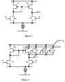
- the figure 2 illustrates a first embodiment of a detection circuit.
- the detection circuit comprises a photodetector 1 which is preferably a photodiode.
- the photodetector comprises a parasitic capacitor C det mounted in parallel with the photodetector 1.
- the photodetector generates a current representative of the observed scene.
- the photodetector can be configured to detect signals in the visible range or in the infrared range.
- the photodetector 1 is connected to a capacitive transimpedance amplifier type reading circuit or CTIA in the English language for Capacitive Translmpedance Amplifier.
- the read circuit comprises an amplifier 2, an input of which is connected to the photodetector 1.
- the other input of the amplifier 2 is connected to a voltage source which applies the voltage V ref .
- the output of the amplifier 2 delivers a voltage signal V out representative of the current signal delivered by the photodetector 1.
- An integrating capacitor C int is connected to the amplifier in a feedback circuit, that is, it connects the output terminal and the first input terminal connected to the photodetector 1.
- noise 1 + VS det VS int .
- V ref * - VS det VS int .
- V ref * and V det * represent the noise components of the voltage V ref and V det .
- the noise level is related to the ratio of the capacitors VS det VS int .
- the electrical capacitance values are related to the performance of the device and are not easily modifiable.
- the voltage V ref and the voltage V det are identical and are provided by the same voltage source so that the noise component supplied by the voltage source is correlated for the voltage V ref applied to a terminal of the amplifier and for the voltage V det applied to a terminal of the photodetector.
- the voltage V det is applied to the photodetector and the amplifier.
- the first voltage source is the second voltage source so that the reference voltage V ref is equal to the detector voltage V det .
- the operational amplifier 2 is unbalanced so as to create a voltage difference between the inverting input and the non-inverting input, that is to say between the two inputs of the amplifier.
- the voltages present on the two inputs of the operational amplifier are identical.
- the voltage V ref is applied to the second input terminal of the amplifier 2 and if the capacitor C int is discharged or lightly charged, the first input terminal of the amplifier is also at the voltage V ref which allows to polarize the photodetector 1.
- V ref voltage which allows to polarize the photodetector 1.
- the voltage difference between the two inputs is less than 10mV in absolute value.
- a detection device which comprises a matrix of photodetectors (for example 1000 photodetectors) associated with a matrix of read circuits (for example 1000 read circuits) of multiple different polarization voltages are observed.
- the operational amplifier 2 In order to ensure a more homogeneous operation of the photodetectors, it is advantageous to unbalance the operational amplifier 2 so that the difference between the inverting and non-inverting inputs is greater than or equal to 20mV and preferably in the range 50.degree. -100mV.
- the amplifier is unbalanced so that the voltage on the first input terminal of the amplifier is shifted from the voltage on the second input terminal of the amplifier of a voltage difference to less than 20mV and preferentially in the range 50-100mV.
- the imbalance is achieved so that the voltage shift is between three and six times the dispersion observed on the transistors.
- the manufacturing variations of the different amplifiers do not disturb the polarization conditions of the photodetector 1.
- the operational amplifier 2 is unbalanced so that the photodetector 1 is reverse biased. In the case where the photodetector 1 is a photodiode, this precaution makes it possible to place the photodiode on the reverse polarization plateau. If a matrix of photodetectors 1 is used in association with a read circuit array, the behavioral variations related to the polarization variation are at least partially erased.
- the first input terminal supplies the voltage V ref .
- the amplifier commonly comprising a current mirror provided with two branches mounted in shunt, it is then possible to provide that one of the branches has different electrical performance of the other branch.
- first and second input terminals are respectively connected to the control electrodes of first and second transistors T3 and T4.
- the imbalance is introduced by using first and second transistors that have different electrical performance.
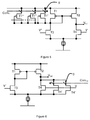
- the figure 3 illustrates a schematic embodiment of an operational amplifier.
- the operational amplifier comprises a current mirror circuit formed by the transistors T1 and T2.
- the inverting and non-inverting inputs are represented by the control electrodes receiving the V - and V + signals.
- the signal V + is applied to the control electrode of the transistor T3.
- the signal V - is applied to the control electrode of the transistor T4.
- Transistors T1 and T3 are connected in series in a first branch while transistors T2 and T4 are connected in series in a second branch. The two branches are connected bypass.
- the transistors are different between the two inputs.
- One way of producing such a device is for example to use transistors having different sizes.
- the transistors T1 and T3 receiving signals V + and V -, that is to say for example the voltage V det, have different dimensions. It is also possible to have transistors T1 and T2 having different dimensions. It is still possible to have a combination of these two embodiments as long as the two branch branches have different electrical performance.
- one of the branches of the current mirror comprises several additional transistors connected in parallel of a main transistor, the additional transistors and the main transistor all receiving the same signal on their control electrode. More specifically, it is possible to provide that the branch provided with the additional transistors comprises a plurality of connection switches 3 connected to enable or block the passage of a current from each associated additional transistor.
- a plurality of additional transistors T2 ', T2 "and T2'" are connected in parallel with the main transistor T2.
- the transistors all receive the same signal on their control electrode.
- the different additional transistors are each coupled to a connection switch 3 which is configured to allow or block the passage of a current to the branch containing the transistor T2.
- These different connection switches 3 are activated separately by the signal Com T2 .
- the signal ComT2 makes it possible to choose whether one or more transistors must be connected in parallel with the transistor T2. In this way, it is possible to choose the amount of current flowing in the branch of the current mirror. The greater the number of connected transistors, the greater the current delivered. By modulating the number of transistors connected in parallel, it is possible to modulate the imbalance between the two branches of the current mirror.
- the transistors T1, T2, T2 ', T2 "and T2'" are identical so as to facilitate the manufacturing process.
- the number of series-connected transistors defines the amplitude of the imbalance.
- the imbalance is achieved on the other branch of the current mirror.
- Several transistors are connected in parallel with the main transistor T1.
- the various additional transistors T1 ', T1 "and T1"' are coupled to connection switches 3 which are activated by the signal Com T1 .
- What has been explained for the embodiment of the figure 4 also applies to the embodiment of the figure 5 by switching the transistors T1 and T2.
- the imbalance is achieved on the transistors receiving the V + and V - signals.
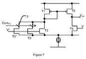
- the embodiments of the figures 6 and 7 represent assemblies for easily unbalancing the operational amplifier.
- the first and second input terminals are respectively connected to the control electrodes of first and second transistors and a plurality of additional transistors are connected in parallel with the first transistor, the additional transistors receiving on their control electrodes the same signal as the first transistor, which may be the transistor T3 or T4. More specifically, it is advantageous to provide that the additional transistors are connected in parallel by means of a plurality of connection switches 3 connected to enable or block the passage of a current from each associated additional transistor.
- the transistor T4 receives the same signal on their control electrode, here the signal V - .
- All additional transistors are also coupled to a connection switch 3 which is configured to allow or block the passage of an additional current in the branch of the operational amplifier.
- the connection switches 3 are activated by means of the signal Com T4 .
- the Com signal T4 makes it possible to define the number of transistors connected in parallel and therefore the difference in current between the two branches.
- the embodiment of the figure 7 illustrates another embodiment where the unbalance of the amplifier is realized by means of several transistors connected in parallel with the transistor T3.
- the multiple transistors connected in parallel make it possible to modulate the amount of current flowing in this branch and therefore the current difference between the two branches.
- the number of transistors involved in the transfer of the current is defined by means of the connection switches 3 and therefore by means of the signal Com T3 which activates the connection switches 3.
- the same voltage source 4 is used to deliver the voltages V ref and V det , but these two voltages are not equal.
- the voltage V ref is obtained from the voltage V det or vice versa. Both voltages are correlated to eliminate the noise component.
- the first voltage source and the second voltage source are formed by means of an initial voltage source supplying a resistive bridge delivering the reference voltage V ref and the detector voltage V det different from the reference voltage V ref .
- the voltage V ref is obtained from the voltage V det by means of a resistive bridge.
- An initial voltage source 5 is used to deliver the voltage V 1 .
- the voltage V 1 is applied to the input of the resistive bridge which delivers the voltages V ref and V det .
- the resistors R1 and R2 are connected in series between the voltage V 1 and the ground and the voltage V ref is delivered by the common terminal to the resistors R1 and R2.
- the resistors R3 and R4 are series mounted and they are together connected in parallel with the resistor R2.
- the voltage V det is delivered by the common terminal to the resistors R3 and R4.
- the reference voltage V ref may be equal to 1.5V.
- the photodetector voltage V det can be shifted from the reference voltage V ref by approximately 200mV.
- the noise level is between 50 and 100 ⁇ V.
- the integration capacitor C int may be of the order of 50 fF.
- the parasitic capacitor C det is about 900 fF.
- the correlation of the voltage sources is advantageous in cooled detection devices, for example in detection devices having an operating temperature below -50 ° C since these devices are generally used to detect low fluxes. It is possible to use photodetectors made on a substrate of Mercury, Cadmium and Tellurium, but other materials are also conceivable.
- the photodetectors are made in a first substrate made of a first semiconductor material and the reading circuits are made in a second substrate made of a second semiconductor material different from the first semiconductor material.
Landscapes
- Engineering & Computer Science (AREA)
- Power Engineering (AREA)
- Multimedia (AREA)
- Signal Processing (AREA)
- Physics & Mathematics (AREA)
- General Physics & Mathematics (AREA)
- Spectroscopy & Molecular Physics (AREA)
- Amplifiers (AREA)
Abstract
Le dispositif de détection comporte un photodétecteur (1) configuré pour transformer un signal électromagnétique en un signal électrique représentatif. Le dispositif de détection comporte également un amplificateur (2) ayant une première borne d'entrée connectée à une première borne du photodétecteur (1). Un condensateur d'intégration (C int ) est connecté à la borne de sortie de l'amplificateur (2) et à la première borne d'entrée de l'amplificateur. Une première source d'une tension de référence (V ref ) est connectée à une deuxième borne d'entrée de l'amplificateur (2). Une deuxième source d'une tension de détecteur (V det ) est connectée à une deuxième borne d'entrée du photodétecteur (1). Les première et deuxième sources de tension (V ref , V det ) sont corrélées de manière à corréler les composantes de bruit.The detection device comprises a photodetector (1) configured to transform an electromagnetic signal into a representative electrical signal. The detection device also includes an amplifier (2) having a first input terminal connected to a first terminal of the photodetector (1). An integrating capacitor (C int) is connected to the output terminal of the amplifier (2) and to the first input terminal of the amplifier. A first source of a reference voltage (V ref) is connected to a second input terminal of the amplifier (2). A second source of a detector voltage (V det) is connected to a second input terminal of the photodetector (1). The first and second voltage sources (V ref, V det) are correlated to correlate the noise components.
Description
L'invention est relative à un dispositif de détection amélioré.The invention relates to an improved detection device.
Dans de nombreuses activités, une scène est observée par un dispositif de détection qui comporte un photodétecteur. Le photodétecteur reçoit un signal lumineux qu'il transforme en un signal électrique représentatif de la scène observée.In many activities, a scene is observed by a detection device that includes a photodetector. The photodetector receives a light signal that transforms into an electrical signal representative of the observed scene.
Dans un mode de réalisation conventionnel illustré à la
Le photodétecteur 1 est relié à un circuit de lecture de type amplificateur transimpédance capacitif ou CTIA en langue anglaise pour Capacitive Translmpedance Amplifier.The photodetector 1 is connected to a capacitive transimpedance amplifier type reading circuit or CTIA in the English language for Capacitive Translmpedance Amplifier.
Le circuit de lecture comporte un amplificateur 2 dont une entrée est reliée au photodétecteur 1. L'autre entrée de l'amplificateur 2 est reliée à une source de tension qui applique la tension Vref. La sortie de l'amplificateur 2 délivre un signal en tension Vout représentatif du signal en courant délivré par le photodétecteur 1.The read circuit comprises an
Un condensateur d'intégration Cint est connecté à l'amplificateur dans un montage en contre-réaction, c'est-à-dire qu'il connecte la borne de sortie et la borne connectée au photodétecteur.An integration capacitor Cint is connected to the amplifier in a feedback arrangement, ie it connects the output terminal and the terminal connected to the photodetector.
Cependant, dans ce type d'architecture, il est observé un bruit sur la borne de sortie qui vient parasiter le signal électrique représentatif de la scène observée.However, in this type of architecture, it is observed a noise on the output terminal that parasitizes the electrical signal representative of the scene observed.
Le rapport signal sur bruit est particulièrement défavorable dans les dispositifs de détection qui présentent des photodétecteurs de taille importante et qui sont configurés pour détecter un très faible flux, c'est-à-dire que le condensateur d'intégration présente une faible capacité électrique et une forte capacité du détecteur.The signal-to-noise ratio is particularly unfavorable in detection devices which have large photodetectors and which are configured to detect a very low flux, that is to say that the integration capacitor has a low electrical capacitance and a strong capacity of the detector.
L'invention a pour objet un dispositif de détection qui présente un rapport signal sur bruit amélioré.The subject of the invention is a detection device which has an improved signal-to-noise ratio.
On tend à atteindre ce résultat au moyen d'un dispositif de détection comportant :
- un photodétecteur configuré pour transformer un signal électromagnétique en un signal électrique représentatif,
- un amplificateur ayant une première borne d'entrée connectée à une première borne du photodétecteur,
- un condensateur d'intégration connecté à la borne de sortie de l'amplificateur et à la première borne d'entrée de l'amplificateur,
- une première source de tension configurée pour délivrer une tension de référence à une deuxième borne d'entrée de l'amplificateur,
- une deuxième source de tension configurée pour délivrer une tension de détecteur à une deuxième borne du photodétecteur,
Le dispositif de détection est remarquable en ce que les première et deuxième sources de tension sont corrélées de manière à corréler les composantes de bruit. De cette manière certaines composantes de bruit s'annulent.
- a photodetector configured to transform an electromagnetic signal into a representative electrical signal,
- an amplifier having a first input terminal connected to a first terminal of the photodetector,
- an integrating capacitor connected to the output terminal of the amplifier and to the first input terminal of the amplifier,
- a first voltage source configured to output a reference voltage to a second input terminal of the amplifier,
- a second voltage source configured to output a detector voltage to a second terminal of the photodetector,
The detection device is notable in that the first and second voltage sources are correlated to correlate the noise components. In this way some noise components cancel each other out.
Il est particulièrement avantageux de prévoir que l'amplificateur est déséquilibré de sorte que la tension sur la première borne d'entrée de l'amplificateur soit décalée de la tension sur la deuxième borne d'entrée de l'amplificateur d'une différence de tension au moins égale à 20mV. Ainsi, les aléas de réalisation ont un effet négligeable sur la conversion du signal lumineux en un signal électrique. De préférence, la différence de tension est comprise entre 50 et 100mV pour réduire encore plus les effets du procédé de réalisation sur un très grand nombre de photodétecteurs et de circuits de lecture.It is particularly advantageous to provide that the amplifier is unbalanced so that the voltage on the first input terminal of the amplifier is offset from the voltage on the second input terminal of the amplifier by a voltage difference at least 20mV. Thus, the unpredictability has a negligible effect on the conversion of the light signal into an electrical signal. Preferably, the voltage difference is between 50 and 100mV to further reduce the effects of the method of production on a very large number of photodetectors and read circuits.
Il est également intéressant de prévoir que l'amplificateur comporte un miroir de courant muni de deux branches montées en dérivation, l'une des branches présentant des performances électriques différentes de l'autre branche. Ainsi, il est possible facilement de réaliser un amplificateur déséquilibré.It is also advantageous to provide that the amplifier comprises a current mirror provided with two branches mounted in shunt, one of the branches having different electrical performance of the other branch. Thus, it is possible to easily realize an unbalanced amplifier.
Dans un cas particulier, l'une des branches du miroir de courant comporte plusieurs transistors additionnels montés en parallèles d'un transistor principal, les transistors additionnels et le transistor principal recevant tous le même signal sur leur électrode de commande. Dans un mode de réalisation plus précis, l'une des branches du miroir de courant comporte plusieurs interrupteurs de connexion connectés pour autoriser ou bloquer le passage d'un courant depuis chaque transistor additionnel associé.In a particular case, one of the branches of the current mirror comprises several additional transistors connected in parallel of a main transistor, the additional transistors and the main transistor all receiving the same signal on their control electrode. In a more precise embodiment, one of the branches of the current mirror has a plurality of connection switches connected to allow or block the passage of a current from each associated additional transistor.
Dans un autre cas particulier, les première et deuxième bornes d'entrée sont connectées respectivement à des électrodes de commande de premier et deuxième transistors et les premier et deuxième transistors présentent des performances électriques différentes.In another particular case, the first and second input terminals are respectively connected to control electrodes of first and second transistors and the first and second transistors have different electrical performances.
Dans un mode de réalisation plus précis, il est possible de prévoir que les première et deuxième bornes d'entrée sont connectées respectivement à des électrodes de commande de premier et deuxième transistors et que plusieurs transistors additionnels sont montés en parallèle du premier transistor, les transistors additionnels recevant sur leurs électrodes de commande le même signal que le premier transistor.In a more precise embodiment, it is possible to provide that the first and second input terminals are respectively connected to control electrodes of the first and second transistors and that several additional transistors are connected in parallel with the first transistor, the additional transistors receiving on their control electrodes the same signal as the first transistor.
Il est encore possible de prévoir que les transistors additionnels sont montés en parallèles au moyen de plusieurs interrupteurs de connexion connectés pour autoriser ou bloquer le passage d'un courant depuis chaque transistor additionnel associé.It is also possible to provide that the additional transistors are connected in parallel by means of a plurality of connection switches connected to enable or block the passage of a current from each associated additional transistor.
Dans un mode de réalisation particulier, la première source de tension est la deuxième source de tension de sorte que la tension de référence est égale à la tension de détecteur.In a particular embodiment, the first voltage source is the second voltage source so that the reference voltage is equal to the detector voltage.
Dans un autre mode de réalisation particulier, la première source de tension et la deuxième source de tension sont formées au moyen d'une source de tension initiale alimentant un pont résistif délivrant la tension de référence et la tension de détecteur différente de la tension de référence.In another particular embodiment, the first voltage source and the second voltage source are formed by means of an initial voltage source supplying a resistive bridge delivering the reference voltage and the detector voltage different from the reference voltage. .
D'autres avantages et caractéristiques ressortiront plus clairement de la description qui va suivre de modes particuliers de réalisation de l'invention donnés à titre d'exemples non limitatifs et représentés aux dessins annexés, dans lesquels :
- la
figure 1 représente, de manière schématique, un circuit de détection de l'art antérieur, - la
figure 2 représente, de manière schématique, un premier mode de réalisation d'un circuit de détection, - la
figure 3 représente, de manière schématique, un premier mode de réalisation d'un amplificateur opérationnel d'un circuit de détection, - les
figures 4 et5 représentent, de manière schématique, des modes de réalisation d'un amplificateur opérationnel avec déséquilibre du miroir de courant, - les
figures 6 et7 représentent, de manière schématique, des modes de réalisation d'un amplificateur opérationnel avec déséquilibre des branches recevant les signaux d'entrée, - la
figure 8 représente, de manière schématique, un autre mode de réalisation d'un circuit de détection.
- the
figure 1 represents, in a schematic manner, a detection circuit of the prior art, - the
figure 2 is a schematic representation of a first embodiment of a detection circuit, - the
figure 3 represents schematically a first embodiment of an operational amplifier of a detection circuit, - the
figures 4 and5 show schematically embodiments of an operational amplifier with imbalance of the current mirror, - the
figures 6 and7 schematically represent embodiments of an operational amplifier with unbalance of the branches receiving the input signals, - the
figure 8 is a schematic representation of another embodiment of a detection circuit.
La
Le circuit de détection comporte un photodétecteur 1 qui est préférentiellement une photodiode. Le photodétecteur comporte un condensateur parasite Cdet monté en parallèle du photodétecteur 1. Le photodétecteur génère un courant représentatif de la scène observée. Le photodétecteur peut être configuré pour détecter des signaux dans le domaine visible ou alors dans le domaine infrarouge.The detection circuit comprises a photodetector 1 which is preferably a photodiode. The photodetector comprises a parasitic capacitor C det mounted in parallel with the photodetector 1. The photodetector generates a current representative of the observed scene. The photodetector can be configured to detect signals in the visible range or in the infrared range.
Le photodétecteur 1 est relié à un circuit de lecture de type amplificateur transimpédance capacitif ou CTIA en langue anglaise pour Capacitive Translmpedance Amplifier.The photodetector 1 is connected to a capacitive transimpedance amplifier type reading circuit or CTIA in the English language for Capacitive Translmpedance Amplifier.
Le circuit de lecture comporte un amplificateur 2 dont une entrée est reliée au photodétecteur 1. L'autre entrée de l'amplificateur 2 est reliée à une source de tension qui applique la tension Vref. La sortie de l'amplificateur 2 délivre un signal en tension Vout représentatif du signal en courant délivré par le photodétecteur 1.The read circuit comprises an
Un condensateur d'intégration Cint est connecté à l'amplificateur dans un montage en contre-réaction, c'est-à-dire qu'il connecte la borne de sortie et la première borne d'entrée connectée au photodétecteur 1.An integrating capacitor C int is connected to the amplifier in a feedback circuit, that is, it connects the output terminal and the first input terminal connected to the photodetector 1.
Dans une telle configuration, une composante du bruit présent sur la borne de sortie délivrant la tension Vout peut s'écrire : ![]()
![]()
Pour réduire la composante de bruit, on remarque qu'il est avantageux d'avoir égalité entre les bruits des tensions Vref* et Vdet* et de fournir les deux tensions au moyen de la même source de tension afin que les composantes du bruit soient corrélés et s'annulent. Vref* et Vdet* représentent les composantes de bruit des tension Vref et Vdet. De cette manière, le bruit généré en sortie du circuit de lecture par les tensions de référence que sont les tensions Vref et Vdet est annulé. On peut également constaté que le niveau du bruit est lié au rapport des condensateurs ![]()
![]()
Dans le mode de réalisation particulier illustré à la
Des essais ont montré que dans ce mode de réalisation, la composante de bruit est annulée ce qui améliore le rapport signal sur bruit.Tests have shown that in this embodiment, the noise component is canceled which improves the signal-to-noise ratio.
Bien que ce mode de réalisation donne de bons résultats, il a été observé que dans une matrice de photodétecteurs associée à une matrice de circuits de lecture, les aléas de fabrication des circuits de lecture entrainent des différences de polarisation appliquée par l'amplificateur 2 sur la borne du photodétecteur 1. Dans certains cas, le photodétecteur 1 est polarisé en inverse, dans d'autres cas le photodétecteur 1 est polarisé en direct et il existe également des cas où la même polarisation est appliquée aux deux bornes du photodétecteur 1.Although this embodiment gives good results, it has been observed that in a matrix of photodetectors associated with a matrix of read circuits, the manufacturing errors of the reading circuits cause differences in the polarization applied by the
Ces variations de polarisation entrainent une différence de comportement du photodétecteur 1 lors de la transformation du signal lumineux en un signal électrique ce qui annule une partie du gain procuré par l'utilisation de la même source de tension sur le niveau de bruit.These polarization variations cause a difference in behavior of the photodetector 1 during the transformation of the light signal into an electrical signal which cancels part of the gain provided by the use of the same voltage source on the noise level.
Dans un mode de réalisation particulier, l'amplificateur opérationnel 2 est déséquilibré de manière à créer une différence de tension entre l'entrée inverseuse et l'entrée non inverseuse, c'est-à-dire entre les deux entrées de l'amplificateur.In a particular embodiment, the
Théoriquement, les tensions présentes sur les deux entrées de l'amplificateur opérationnel sont identiques. Par exemple, lorsque la tension Vref est appliquée sur la deuxième borne d'entrée de l'amplificateur 2 et si le condensateur Cint est déchargé ou faiblement chargé, la première borne d'entrée de l'amplificateur est également à la tension Vref ce qui permet de polariser le photodétecteur 1. Un tel mode de réalisation est illustré à la
Dans la pratique, lorsque plusieurs amplificateurs opérationnels sont réalisés, il existe une légère différence de tension entre les différents amplificateurs et la valeur de cette différence varie d'un amplificateur à un autre. De manière classique, la différence de tension entre les deux entrées (également appelées entrées inverseuse et non inverseuse) est inférieure à 10mV en valeur absolue. Dans un dispositif de détection qui comporte une matrice de photodétecteurs (par exemple 1000 photodétecteurs) associée à une matrice de circuits de lecture (par exemple 1000 circuits de lecture) de multiples tensions différentes de polarisation sont observées.In practice, when several operational amplifiers are made, there is a slight difference in voltage between the different amplifiers and the The value of this difference varies from one amplifier to another. In a conventional manner, the voltage difference between the two inputs (also called inverting and non-inverting inputs) is less than 10mV in absolute value. In a detection device which comprises a matrix of photodetectors (for example 1000 photodetectors) associated with a matrix of read circuits (for example 1000 read circuits) of multiple different polarization voltages are observed.
De manière à s'assurer un fonctionnement plus homogène des photodétecteurs, il est avantageux de déséquilibrer l'amplificateur opérationnel 2 de manière à ce que la différence entre les entrées inverseuse et non inverseuse soit supérieure ou égale à 20mV et de préférence dans la gamme 50-100mV. En d'autres termes, l'amplificateur est déséquilibré de sorte que la tension sur la première borne d'entrée de l'amplificateur soit décalée de la tension sur la deuxième borne d'entrée de l'amplificateur d'une différence de tension au moins égale à 20mV et préférentiellement dans la gamme 50-100mV. De manière préférentielle, le déséquilibre est réalisé de manière à ce que le décalage de tension soit entre trois et six fois la dispersion observée sur les transistors.In order to ensure a more homogeneous operation of the photodetectors, it is advantageous to unbalance the
Dans ces conditions, les variations de fabrication des différents amplificateurs ne viennent pas perturber les conditions de polarisation du photodétecteur 1. De manière particulièrement avantageuse, l'amplificateur opérationnel 2 est déséquilibré de manière à ce que le photodétecteur 1 soit polarisé en inverse. Dans le cas où le photodétecteur 1 est une photodiode, cette précaution permet de placer la photodiode sur le plateau de polarisation inverse. Si une matrice de photodétecteurs 1 est utilisée en association avec une matrice de circuits de lecture, les variations de comportement liées aux variation de polarisation sont au moins partiellement gommées.Under these conditions, the manufacturing variations of the different amplifiers do not disturb the polarization conditions of the photodetector 1. Particularly advantageously, the
Dans ce cas de figure, bien que la tension Vdet soit appliquée sur la deuxième borne d'entrée de l'amplificateur 2, la première borne d'entrée délivre la tension Vref.In this case, although the voltage V det is applied to the second input terminal of the
Pour déséquilibrer un amplificateur, de nombreux modes de réalisation existent. Une manière simple est de déséquilibrer les deux branches connectées aux deux entrées de l'amplificateur. Dans de nombreux modes de réalisation, les deux branches sont montées en dérivation. Il est alors intéressant de présenter deux branches qui comportent des performances électriques différentes.To unbalance an amplifier, many embodiments exist. A simple way is to unbalance the two branches connected to the two inputs of the amplifier. In many embodiments, the two branches are shunted. It is therefore interesting to present two branches that have different electrical performance.
L'amplificateur comportant communément un miroir de courant muni de deux branches montées en dérivation, il est alors possible de prévoir que l'une des branches présente des performances électriques différentes de l'autre branche.The amplifier commonly comprising a current mirror provided with two branches mounted in shunt, it is then possible to provide that one of the branches has different electrical performance of the other branch.
Dans un autre mode de réalisation, les première et deuxième bornes d'entrée sont connectées respectivement aux électrodes de commandes de premier et deuxième transistors T3 et T4. Le déséquilibre est introduit en utilisant des premier et deuxième transistors qui présentent des performances électriques différentes.In another embodiment, the first and second input terminals are respectively connected to the control electrodes of first and second transistors T3 and T4. The imbalance is introduced by using first and second transistors that have different electrical performance.
La
Les transistors T1 et T3 sont montés en série dans une première branche alors que les transistors T2 et T4 sont montés en série dans une deuxième branche. Les deux branches sont montées en dérivation.Transistors T1 and T3 are connected in series in a first branch while transistors T2 and T4 are connected in series in a second branch. The two branches are connected bypass.
Pour réaliser une différence de tension entre les entrées inverseuse et non inverseuse, il est possible de déséquilibrer l'amplificateur opérationnel au moyen de transistors ayant des performances électriques différentes. Alors que dans un amplificateur opérationnel classique, on utilise des transistors identiques pour les entrées inverseuse et non inverseuse, dans ce mode de réalisation les transistors sont différents entre les deux entrées. Une manière de réaliser un tel dispositif est par exemple d'utiliser des transistors ayant des tailles différentes. Les transistors T1 et T3 recevant les signaux V+ et V-, c'est-à-dire par exemple la tension Vdet, ont des dimensions différentes. Il est également possible d'avoir des transistors T1 et T2 ayant des dimensions différentes. Il est encore possible d'avoir une combinaison de ces deux modes de réalisation tant que les deux branches montées en dérivation présentent des performances électriques différentes.To achieve a voltage difference between the inverting and non-inverting inputs, it is possible to unbalance the operational amplifier by means of transistors having different electrical performances. While in a conventional operational amplifier, identical transistors are used for the inverting and non-inverting inputs, in this embodiment the transistors are different between the two inputs. One way of producing such a device is for example to use transistors having different sizes. The transistors T1 and T3 receiving signals V + and V -, that is to say for example the voltage V det, have different dimensions. It is also possible to have transistors T1 and T2 having different dimensions. It is still possible to have a combination of these two embodiments as long as the two branch branches have different electrical performance.
Les
Dans le mode de réalisation de la
En choisissant un transistor T1 plus grand que le transistor T2, il est possible d'avoir un déséquilibre dans un premier sens entre les deux branches du miroir de courant puis d'annuler le déséquilibre ou d'inverser le déséquilibre en augmentant le nombre de transistors montés en parallèle du transistor T2.By choosing a transistor T1 larger than the transistor T2, it is possible to have an imbalance in a first direction between the two branches of the current mirror and then cancel the imbalance or reverse the imbalance by increasing the number of transistors connected in parallel with the transistor T2.
De manière avantageuse, les transistors T1, T2, T2', T2" et T2'" sont identiques de manière à faciliter le procédé de fabrication. Le nombre de transistors montés en série définit l'amplitude du déséquilibre.Advantageously, the transistors T1, T2, T2 ', T2 "and T2'" are identical so as to facilitate the manufacturing process. The number of series-connected transistors defines the amplitude of the imbalance.
Dans le mode de réalisation de la
Il est aussi possible de combiner ces deux modes de réalisation.It is also possible to combine these two embodiments.
Dans une variante de réalisation, le déséquilibre est réalisé sur les transistors recevant les signaux V+ et V-. Les modes de réalisation des
Dans le mode de réalisation de la
Le mode de réalisation de la
Les modes de réalisation des
Ces différents modes de réalisation sont particulièrement avantageux car ils permettent de conserver un dispositif compact et facilement réalisable.These various embodiments are particularly advantageous because they make it possible to maintain a compact and easily achievable device.
Dans une variante de réalisation illustrée à la
Dans le mode de réalisation illustré à la
A titre d'exemple, les résistances R1 et R2 sont montées en série entre la tension V1 et la masse et la tension Vref est délivrée par la borne commune aux résistances R1 et R2. Les résistances R3 et R4 sont montées série et elles sont ensemble montées en parallèle de la résistance R2. La tension Vdet est délivrée par la borne commune aux résistances R3 et R4 En fonction, des valeurs des résistances R1, R2, R3 et R4, il est possible de définir les tensions Vref et Vdet par rapport à la tension V1.By way of example, the resistors R1 and R2 are connected in series between the voltage V 1 and the ground and the voltage V ref is delivered by the common terminal to the resistors R1 and R2. The resistors R3 and R4 are series mounted and they are together connected in parallel with the resistor R2. The voltage V det is delivered by the common terminal to the resistors R3 and R4. Depending on the values of the resistors R1, R2, R3 and R4, it is possible to define the voltages V ref and V det with respect to the voltage V 1 .
A titre d'exemple, la tension de référence Vref peut être égale à 1,5V. La tension de photodétecteur Vdet peut être décalée de la tension de référence Vref d'environ 200mV.For example, the reference voltage V ref may be equal to 1.5V. The photodetector voltage V det can be shifted from the reference voltage V ref by approximately 200mV.
Pour une source de tension conventionnelle, le niveau de bruit est compris entre 50 et 100µV.For a conventional voltage source, the noise level is between 50 and 100μV.
Pour la détection d'un faible signal, le condensateur d'intégration Cint peut être de l'ordre de 50fF. Dans les conditions standards de réalisation, le condensateur parasite Cdet est d'environ 900fF.For the detection of a weak signal, the integration capacitor C int may be of the order of 50 fF. Under standard conditions of realization, the parasitic capacitor C det is about 900 fF.
Pour un tel dispositif de détection, il a été observé une nette amélioration du rapport signal sur bruit en utilisant des source de tension Vref et Vdet corrélées.For such a detection device, a marked improvement in the signal-to-noise ratio has been observed by using correlated voltage sources V ref and V det .
La corrélation des sources de tension est avantageuse dans les dispositifs de détection refroidis, par exemple dans les dispositifs de détection ayant une température de fonctionnement inférieure à -50°C car ces dispositifs sont généralement utilisés pour détecter des faibles flux. Il est possible d'utiliser des photodétecteurs réalisés sur un substrat de Mercure, Cadmium et Tellure, mais d'autres matériaux sont également envisageables.The correlation of the voltage sources is advantageous in cooled detection devices, for example in detection devices having an operating temperature below -50 ° C since these devices are generally used to detect low fluxes. It is possible to use photodetectors made on a substrate of Mercury, Cadmium and Tellurium, but other materials are also conceivable.
Dans les dispositifs de détections refroidis, les photodétecteurs sont réalisés dans un premier substrat en un premier matériau semi-conducteur et les circuits de lecture sont réalisés dans un deuxième substrat en un deuxième matériau semi-conducteur différent du premier matériau semi-conducteur.In the cooled detection devices, the photodetectors are made in a first substrate made of a first semiconductor material and the reading circuits are made in a second substrate made of a second semiconductor material different from the first semiconductor material.
Claims (11)
de détecteur (Vdet) à une deuxième borne du photodétecteur (1), dispositif de détection caractérisé en ce que les première et deuxième sources de tension (Vref, Vdet) sont corrélées de manière à corréler les composantes de bruit.
detector (V det ) at a second terminal of the photodetector (1), detection device characterized in that the first and second voltage sources (V ref , V det ) are correlated so as to correlate the noise components.
Applications Claiming Priority (1)
| Application Number | Priority Date | Filing Date | Title |
|---|---|---|---|
| FR1551132A FR3032853B1 (en) | 2015-02-12 | 2015-02-12 | IMPROVED DETECTION DEVICE |
Publications (2)
| Publication Number | Publication Date |
|---|---|
| EP3057311A1 true EP3057311A1 (en) | 2016-08-17 |
| EP3057311B1 EP3057311B1 (en) | 2020-09-02 |
Family
ID=53674020
Family Applications (1)
| Application Number | Title | Priority Date | Filing Date |
|---|---|---|---|
| EP16155440.7A Active EP3057311B1 (en) | 2015-02-12 | 2016-02-12 | Improved detection device |
Country Status (4)
| Country | Link |
|---|---|
| US (1) | US10066988B2 (en) |
| EP (1) | EP3057311B1 (en) |
| FR (1) | FR3032853B1 (en) |
| IL (1) | IL244094B (en) |
Citations (4)
| Publication number | Priority date | Publication date | Assignee | Title |
|---|---|---|---|---|
| FR2593319A1 (en) * | 1986-01-17 | 1987-07-24 | Thomson Csf | PHOTOSENSITIVE ELEMENT READING METHOD COMPRISING A PHOTODIODE AND A CAPACITY |
| US6097021A (en) * | 1997-01-06 | 2000-08-01 | Texas Instruments Incorporated | Apparatus and method for a managed integration optical sensor array |
| EP0845687B1 (en) * | 1996-11-27 | 2002-05-22 | General Electric Company | Solid state area X-ray detector with adjustable bias |
| US20140061488A1 (en) * | 2012-08-31 | 2014-03-06 | Canon Kabushiki Kaisha | Radiation imaging apparatus and radiation imaging system |
Family Cites Families (3)
| Publication number | Priority date | Publication date | Assignee | Title |
|---|---|---|---|---|
| US4889985A (en) * | 1988-10-26 | 1989-12-26 | Tektronix, Inc. | Combined optical power meter and receiver |
| US7773134B2 (en) * | 2004-03-15 | 2010-08-10 | Avago Technologies Ecbu Ip (Singapore) Pte. Ltd. | System and method for canceling dark photocurrent in a color sensor circuit |
| JP6164798B2 (en) * | 2012-04-04 | 2017-07-19 | キヤノン株式会社 | Radiation imaging apparatus, radiation imaging system, and method for controlling radiation imaging apparatus |
-
2015
- 2015-02-12 FR FR1551132A patent/FR3032853B1/en active Active
-
2016
- 2016-02-11 IL IL24409416A patent/IL244094B/en active IP Right Grant
- 2016-02-11 US US15/041,496 patent/US10066988B2/en active Active
- 2016-02-12 EP EP16155440.7A patent/EP3057311B1/en active Active
Patent Citations (4)
| Publication number | Priority date | Publication date | Assignee | Title |
|---|---|---|---|---|
| FR2593319A1 (en) * | 1986-01-17 | 1987-07-24 | Thomson Csf | PHOTOSENSITIVE ELEMENT READING METHOD COMPRISING A PHOTODIODE AND A CAPACITY |
| EP0845687B1 (en) * | 1996-11-27 | 2002-05-22 | General Electric Company | Solid state area X-ray detector with adjustable bias |
| US6097021A (en) * | 1997-01-06 | 2000-08-01 | Texas Instruments Incorporated | Apparatus and method for a managed integration optical sensor array |
| US20140061488A1 (en) * | 2012-08-31 | 2014-03-06 | Canon Kabushiki Kaisha | Radiation imaging apparatus and radiation imaging system |
Also Published As
| Publication number | Publication date |
|---|---|
| FR3032853A1 (en) | 2016-08-19 |
| IL244094B (en) | 2019-10-31 |
| IL244094A0 (en) | 2016-07-31 |
| EP3057311B1 (en) | 2020-09-02 |
| US10066988B2 (en) | 2018-09-04 |
| FR3032853B1 (en) | 2017-02-17 |
| US20160238446A1 (en) | 2016-08-18 |
Similar Documents
| Publication | Publication Date | Title |
|---|---|---|
| FR2654274A1 (en) | METHOD AND CIRCUIT FOR CANCELING HARMONIC DISTORTION INDUCED BY NONLINEAR CAPACITY. | |
| EP2600125B1 (en) | Radiation-detection device with improved illumination range | |
| FR2623307A1 (en) | TWO-TERMINAL CURRENT SOURCE WITH TEMPERATURE COMPENSATION | |
| FR2558659A1 (en) | POLARIZATION CIRCUIT OF A FIELD EFFECT TRANSISTOR | |
| EP1647091B1 (en) | Low-consumption voltage amplifier | |
| FR3071116B1 (en) | DEVICE THAT MODIFIES THE VALUE OF IMPEDANCE OF A REFERENCE RESISTANCE | |
| EP3057311B1 (en) | Improved detection device | |
| FR2623347A1 (en) | ||
| EP2463632B1 (en) | Detection device comprising a robust test circuit | |
| EP1313309A1 (en) | Calibrating device for a video input stage | |
| EP3451181B1 (en) | Circuit for protecting against high voltages for usb type c receiver | |
| EP3114442B1 (en) | Light-ray detection circuit | |
| EP1102148B1 (en) | Low temperature corrected voltage generating device | |
| EP0750782B1 (en) | Fast differential sample-and-hold circuit | |
| FR2601208A1 (en) | LOW HARMONIC DISTORTION VOLTAGE REPEATER CIRCUIT FOR RESISTIVE COMPONENT LOADS | |
| EP2783192B1 (en) | Detection circuit with a noise-reduction module | |
| EP0568474B1 (en) | MOS circuit for separating a synchronising signal in a composite video signal | |
| FR2822308A1 (en) | Circuit for separating poles between two stages of amplifier circuit, based on Miller effect and comprising resistive voltage divider bridge and two capacitors in serial branch | |
| FR2755805A1 (en) | AMPLIFICATION CIRCUIT COMPRISING AN INPUT CURRENT COMPENSATION DEVICE | |
| EP2309726B1 (en) | Detection circuit with bypass of a part of the photodetector current | |
| EP1487106A1 (en) | Integrated circuit producing power supply independent logic levels without regulators in the power section and a corresponding communication module. | |
| FR2552949A1 (en) | Squelch cascode circuit with dead zone | |
| FR2941305A1 (en) | AMPLIFICATION STRUCTURE AND DETECTION AND MEASURING CHAIN COMPRISING SUCH A STRUCTURE. |
Legal Events
| Date | Code | Title | Description |
|---|---|---|---|
| PUAI | Public reference made under article 153(3) epc to a published international application that has entered the european phase |
Free format text: ORIGINAL CODE: 0009012 |
|
| AK | Designated contracting states |
Kind code of ref document: A1 Designated state(s): AL AT BE BG CH CY CZ DE DK EE ES FI FR GB GR HR HU IE IS IT LI LT LU LV MC MK MT NL NO PL PT RO RS SE SI SK SM TR |
|
| AX | Request for extension of the european patent |
Extension state: BA ME |
|
| STAA | Information on the status of an ep patent application or granted ep patent |
Free format text: STATUS: REQUEST FOR EXAMINATION WAS MADE |
|
| 17P | Request for examination filed |
Effective date: 20170214 |
|
| RBV | Designated contracting states (corrected) |
Designated state(s): AL AT BE BG CH CY CZ DE DK EE ES FI FR GB GR HR HU IE IS IT LI LT LU LV MC MK MT NL NO PL PT RO RS SE SI SK SM TR |
|
| STAA | Information on the status of an ep patent application or granted ep patent |
Free format text: STATUS: EXAMINATION IS IN PROGRESS |
|
| 17Q | First examination report despatched |
Effective date: 20180716 |
|
| RAP1 | Party data changed (applicant data changed or rights of an application transferred) |
Owner name: LYNRED |
|
| GRAP | Despatch of communication of intention to grant a patent |
Free format text: ORIGINAL CODE: EPIDOSNIGR1 |
|
| STAA | Information on the status of an ep patent application or granted ep patent |
Free format text: STATUS: GRANT OF PATENT IS INTENDED |
|
| INTG | Intention to grant announced |
Effective date: 20200327 |
|
| RIC1 | Information provided on ipc code assigned before grant |
Ipc: H04N 5/335 20110101ALI20200314BHEP Ipc: H04N 5/378 20110101ALI20200314BHEP Ipc: H03F 3/45 20060101ALN20200314BHEP Ipc: H03F 3/08 20060101ALI20200314BHEP Ipc: H04N 5/3745 20110101AFI20200314BHEP |
|
| GRAS | Grant fee paid |
Free format text: ORIGINAL CODE: EPIDOSNIGR3 |
|
| GRAA | (expected) grant |
Free format text: ORIGINAL CODE: 0009210 |
|
| STAA | Information on the status of an ep patent application or granted ep patent |
Free format text: STATUS: THE PATENT HAS BEEN GRANTED |
|
| AK | Designated contracting states |
Kind code of ref document: B1 Designated state(s): AL AT BE BG CH CY CZ DE DK EE ES FI FR GB GR HR HU IE IS IT LI LT LU LV MC MK MT NL NO PL PT RO RS SE SI SK SM TR |
|
| REG | Reference to a national code |
Ref country code: GB Ref legal event code: FG4D Free format text: NOT ENGLISH |
|
| REG | Reference to a national code |
Ref country code: AT Ref legal event code: REF Ref document number: 1310168 Country of ref document: AT Kind code of ref document: T Effective date: 20200915 Ref country code: CH Ref legal event code: EP |
|
| REG | Reference to a national code |
Ref country code: DE Ref legal event code: R096 Ref document number: 602016043037 Country of ref document: DE |
|
| REG | Reference to a national code |
Ref country code: IE Ref legal event code: FG4D Free format text: LANGUAGE OF EP DOCUMENT: FRENCH |
|
| REG | Reference to a national code |
Ref country code: SE Ref legal event code: TRGR |
|
| REG | Reference to a national code |
Ref country code: LT Ref legal event code: MG4D |
|
| PG25 | Lapsed in a contracting state [announced via postgrant information from national office to epo] |
Ref country code: HR Free format text: LAPSE BECAUSE OF FAILURE TO SUBMIT A TRANSLATION OF THE DESCRIPTION OR TO PAY THE FEE WITHIN THE PRESCRIBED TIME-LIMIT Effective date: 20200902 Ref country code: BG Free format text: LAPSE BECAUSE OF FAILURE TO SUBMIT A TRANSLATION OF THE DESCRIPTION OR TO PAY THE FEE WITHIN THE PRESCRIBED TIME-LIMIT Effective date: 20201202 Ref country code: GR Free format text: LAPSE BECAUSE OF FAILURE TO SUBMIT A TRANSLATION OF THE DESCRIPTION OR TO PAY THE FEE WITHIN THE PRESCRIBED TIME-LIMIT Effective date: 20201203 Ref country code: NO Free format text: LAPSE BECAUSE OF FAILURE TO SUBMIT A TRANSLATION OF THE DESCRIPTION OR TO PAY THE FEE WITHIN THE PRESCRIBED TIME-LIMIT Effective date: 20201202 Ref country code: FI Free format text: LAPSE BECAUSE OF FAILURE TO SUBMIT A TRANSLATION OF THE DESCRIPTION OR TO PAY THE FEE WITHIN THE PRESCRIBED TIME-LIMIT Effective date: 20200902 Ref country code: LT Free format text: LAPSE BECAUSE OF FAILURE TO SUBMIT A TRANSLATION OF THE DESCRIPTION OR TO PAY THE FEE WITHIN THE PRESCRIBED TIME-LIMIT Effective date: 20200902 |
|
| REG | Reference to a national code |
Ref country code: NL Ref legal event code: MP Effective date: 20200902 |
|
| REG | Reference to a national code |
Ref country code: AT Ref legal event code: MK05 Ref document number: 1310168 Country of ref document: AT Kind code of ref document: T Effective date: 20200902 |
|
| PG25 | Lapsed in a contracting state [announced via postgrant information from national office to epo] |
Ref country code: LV Free format text: LAPSE BECAUSE OF FAILURE TO SUBMIT A TRANSLATION OF THE DESCRIPTION OR TO PAY THE FEE WITHIN THE PRESCRIBED TIME-LIMIT Effective date: 20200902 Ref country code: RS Free format text: LAPSE BECAUSE OF FAILURE TO SUBMIT A TRANSLATION OF THE DESCRIPTION OR TO PAY THE FEE WITHIN THE PRESCRIBED TIME-LIMIT Effective date: 20200902 Ref country code: PL Free format text: LAPSE BECAUSE OF FAILURE TO SUBMIT A TRANSLATION OF THE DESCRIPTION OR TO PAY THE FEE WITHIN THE PRESCRIBED TIME-LIMIT Effective date: 20200902 |
|
| PG25 | Lapsed in a contracting state [announced via postgrant information from national office to epo] |
Ref country code: PT Free format text: LAPSE BECAUSE OF FAILURE TO SUBMIT A TRANSLATION OF THE DESCRIPTION OR TO PAY THE FEE WITHIN THE PRESCRIBED TIME-LIMIT Effective date: 20210104 Ref country code: RO Free format text: LAPSE BECAUSE OF FAILURE TO SUBMIT A TRANSLATION OF THE DESCRIPTION OR TO PAY THE FEE WITHIN THE PRESCRIBED TIME-LIMIT Effective date: 20200902 Ref country code: SM Free format text: LAPSE BECAUSE OF FAILURE TO SUBMIT A TRANSLATION OF THE DESCRIPTION OR TO PAY THE FEE WITHIN THE PRESCRIBED TIME-LIMIT Effective date: 20200902 Ref country code: EE Free format text: LAPSE BECAUSE OF FAILURE TO SUBMIT A TRANSLATION OF THE DESCRIPTION OR TO PAY THE FEE WITHIN THE PRESCRIBED TIME-LIMIT Effective date: 20200902 Ref country code: NL Free format text: LAPSE BECAUSE OF FAILURE TO SUBMIT A TRANSLATION OF THE DESCRIPTION OR TO PAY THE FEE WITHIN THE PRESCRIBED TIME-LIMIT Effective date: 20200902 Ref country code: CZ Free format text: LAPSE BECAUSE OF FAILURE TO SUBMIT A TRANSLATION OF THE DESCRIPTION OR TO PAY THE FEE WITHIN THE PRESCRIBED TIME-LIMIT Effective date: 20200902 |
|
| PG25 | Lapsed in a contracting state [announced via postgrant information from national office to epo] |
Ref country code: AL Free format text: LAPSE BECAUSE OF FAILURE TO SUBMIT A TRANSLATION OF THE DESCRIPTION OR TO PAY THE FEE WITHIN THE PRESCRIBED TIME-LIMIT Effective date: 20200902 Ref country code: AT Free format text: LAPSE BECAUSE OF FAILURE TO SUBMIT A TRANSLATION OF THE DESCRIPTION OR TO PAY THE FEE WITHIN THE PRESCRIBED TIME-LIMIT Effective date: 20200902 Ref country code: ES Free format text: LAPSE BECAUSE OF FAILURE TO SUBMIT A TRANSLATION OF THE DESCRIPTION OR TO PAY THE FEE WITHIN THE PRESCRIBED TIME-LIMIT Effective date: 20200902 Ref country code: IS Free format text: LAPSE BECAUSE OF FAILURE TO SUBMIT A TRANSLATION OF THE DESCRIPTION OR TO PAY THE FEE WITHIN THE PRESCRIBED TIME-LIMIT Effective date: 20210102 |
|
| REG | Reference to a national code |
Ref country code: DE Ref legal event code: R097 Ref document number: 602016043037 Country of ref document: DE |
|
| PG25 | Lapsed in a contracting state [announced via postgrant information from national office to epo] |
Ref country code: SK Free format text: LAPSE BECAUSE OF FAILURE TO SUBMIT A TRANSLATION OF THE DESCRIPTION OR TO PAY THE FEE WITHIN THE PRESCRIBED TIME-LIMIT Effective date: 20200902 |
|
| PLBE | No opposition filed within time limit |
Free format text: ORIGINAL CODE: 0009261 |
|
| STAA | Information on the status of an ep patent application or granted ep patent |
Free format text: STATUS: NO OPPOSITION FILED WITHIN TIME LIMIT |
|
| 26N | No opposition filed |
Effective date: 20210603 |
|
| PG25 | Lapsed in a contracting state [announced via postgrant information from national office to epo] |
Ref country code: DK Free format text: LAPSE BECAUSE OF FAILURE TO SUBMIT A TRANSLATION OF THE DESCRIPTION OR TO PAY THE FEE WITHIN THE PRESCRIBED TIME-LIMIT Effective date: 20200902 Ref country code: SI Free format text: LAPSE BECAUSE OF FAILURE TO SUBMIT A TRANSLATION OF THE DESCRIPTION OR TO PAY THE FEE WITHIN THE PRESCRIBED TIME-LIMIT Effective date: 20200902 |
|
| PG25 | Lapsed in a contracting state [announced via postgrant information from national office to epo] |
Ref country code: MC Free format text: LAPSE BECAUSE OF FAILURE TO SUBMIT A TRANSLATION OF THE DESCRIPTION OR TO PAY THE FEE WITHIN THE PRESCRIBED TIME-LIMIT Effective date: 20200902 |
|
| REG | Reference to a national code |
Ref country code: BE Ref legal event code: MM Effective date: 20210228 |
|
| PG25 | Lapsed in a contracting state [announced via postgrant information from national office to epo] |
Ref country code: LU Free format text: LAPSE BECAUSE OF NON-PAYMENT OF DUE FEES Effective date: 20210212 Ref country code: LI Free format text: LAPSE BECAUSE OF NON-PAYMENT OF DUE FEES Effective date: 20210228 Ref country code: CH Free format text: LAPSE BECAUSE OF NON-PAYMENT OF DUE FEES Effective date: 20210228 Ref country code: IT Free format text: LAPSE BECAUSE OF FAILURE TO SUBMIT A TRANSLATION OF THE DESCRIPTION OR TO PAY THE FEE WITHIN THE PRESCRIBED TIME-LIMIT Effective date: 20200902 |
|
| PG25 | Lapsed in a contracting state [announced via postgrant information from national office to epo] |
Ref country code: IE Free format text: LAPSE BECAUSE OF NON-PAYMENT OF DUE FEES Effective date: 20210212 |
|
| PG25 | Lapsed in a contracting state [announced via postgrant information from national office to epo] |
Ref country code: BE Free format text: LAPSE BECAUSE OF NON-PAYMENT OF DUE FEES Effective date: 20210228 |
|
| REG | Reference to a national code |
Ref country code: DE Ref legal event code: R079 Ref document number: 602016043037 Country of ref document: DE Free format text: PREVIOUS MAIN CLASS: H04N0005374500 Ipc: H04N0025770000 |
|
| PGFP | Annual fee paid to national office [announced via postgrant information from national office to epo] |
Ref country code: FR Payment date: 20230227 Year of fee payment: 8 |
|
| PG25 | Lapsed in a contracting state [announced via postgrant information from national office to epo] |
Ref country code: HU Free format text: LAPSE BECAUSE OF FAILURE TO SUBMIT A TRANSLATION OF THE DESCRIPTION OR TO PAY THE FEE WITHIN THE PRESCRIBED TIME-LIMIT; INVALID AB INITIO Effective date: 20160212 |
|
| PGFP | Annual fee paid to national office [announced via postgrant information from national office to epo] |
Ref country code: SE Payment date: 20230224 Year of fee payment: 8 |
|
| PG25 | Lapsed in a contracting state [announced via postgrant information from national office to epo] |
Ref country code: CY Free format text: LAPSE BECAUSE OF FAILURE TO SUBMIT A TRANSLATION OF THE DESCRIPTION OR TO PAY THE FEE WITHIN THE PRESCRIBED TIME-LIMIT Effective date: 20200902 |
|
| PG25 | Lapsed in a contracting state [announced via postgrant information from national office to epo] |
Ref country code: MK Free format text: LAPSE BECAUSE OF FAILURE TO SUBMIT A TRANSLATION OF THE DESCRIPTION OR TO PAY THE FEE WITHIN THE PRESCRIBED TIME-LIMIT Effective date: 20200902 |
|
| PGFP | Annual fee paid to national office [announced via postgrant information from national office to epo] |
Ref country code: DE Payment date: 20240216 Year of fee payment: 9 Ref country code: GB Payment date: 20240222 Year of fee payment: 9 |