EP3057123A1 - Joining structure and electronic member-joining structural body - Google Patents
Joining structure and electronic member-joining structural body Download PDFInfo
- Publication number
- EP3057123A1 EP3057123A1 EP14851457.3A EP14851457A EP3057123A1 EP 3057123 A1 EP3057123 A1 EP 3057123A1 EP 14851457 A EP14851457 A EP 14851457A EP 3057123 A1 EP3057123 A1 EP 3057123A1
- Authority
- EP
- European Patent Office
- Prior art keywords
- grain size
- crystal grain
- metal
- porous body
- outer layer
- Prior art date
- Legal status (The legal status is an assumption and is not a legal conclusion. Google has not performed a legal analysis and makes no representation as to the accuracy of the status listed.)
- Granted
Links
Images


Classifications
-
- B—PERFORMING OPERATIONS; TRANSPORTING
- B22—CASTING; POWDER METALLURGY
- B22F—WORKING METALLIC POWDER; MANUFACTURE OF ARTICLES FROM METALLIC POWDER; MAKING METALLIC POWDER; APPARATUS OR DEVICES SPECIALLY ADAPTED FOR METALLIC POWDER
- B22F7/00—Manufacture of composite layers, workpieces, or articles, comprising metallic powder, by sintering the powder, with or without compacting wherein at least one part is obtained by sintering or compression
- B22F7/002—Manufacture of composite layers, workpieces, or articles, comprising metallic powder, by sintering the powder, with or without compacting wherein at least one part is obtained by sintering or compression of porous nature
- B22F7/004—Manufacture of composite layers, workpieces, or articles, comprising metallic powder, by sintering the powder, with or without compacting wherein at least one part is obtained by sintering or compression of porous nature comprising at least one non-porous part
-
- H—ELECTRICITY
- H10—SEMICONDUCTOR DEVICES; ELECTRIC SOLID-STATE DEVICES NOT OTHERWISE PROVIDED FOR
- H10W—GENERIC PACKAGES, INTERCONNECTIONS, CONNECTORS OR OTHER CONSTRUCTIONAL DETAILS OF DEVICES COVERED BY CLASS H10
- H10W40/00—Arrangements for thermal protection or thermal control
- H10W40/20—Arrangements for cooling
- H10W40/25—Arrangements for cooling characterised by their materials
- H10W40/255—Arrangements for cooling characterised by their materials having a laminate or multilayered structure, e.g. direct bond copper [DBC] ceramic substrates
-
- H—ELECTRICITY
- H10—SEMICONDUCTOR DEVICES; ELECTRIC SOLID-STATE DEVICES NOT OTHERWISE PROVIDED FOR
- H10W—GENERIC PACKAGES, INTERCONNECTIONS, CONNECTORS OR OTHER CONSTRUCTIONAL DETAILS OF DEVICES COVERED BY CLASS H10
- H10W70/00—Package substrates; Interposers; Redistribution layers [RDL]
- H10W70/01—Manufacture or treatment
- H10W70/02—Manufacture or treatment of conductive package substrates serving as an interconnection, e.g. of metal plates
-
- H—ELECTRICITY
- H10—SEMICONDUCTOR DEVICES; ELECTRIC SOLID-STATE DEVICES NOT OTHERWISE PROVIDED FOR
- H10W—GENERIC PACKAGES, INTERCONNECTIONS, CONNECTORS OR OTHER CONSTRUCTIONAL DETAILS OF DEVICES COVERED BY CLASS H10
- H10W70/00—Package substrates; Interposers; Redistribution layers [RDL]
- H10W70/01—Manufacture or treatment
- H10W70/05—Manufacture or treatment of insulating or insulated package substrates, or of interposers, or of redistribution layers
-
- H—ELECTRICITY
- H10—SEMICONDUCTOR DEVICES; ELECTRIC SOLID-STATE DEVICES NOT OTHERWISE PROVIDED FOR
- H10W—GENERIC PACKAGES, INTERCONNECTIONS, CONNECTORS OR OTHER CONSTRUCTIONAL DETAILS OF DEVICES COVERED BY CLASS H10
- H10W70/00—Package substrates; Interposers; Redistribution layers [RDL]
- H10W70/60—Insulating or insulated package substrates; Interposers; Redistribution layers
- H10W70/62—Insulating or insulated package substrates; Interposers; Redistribution layers characterised by their interconnections
- H10W70/66—Conductive materials thereof
-
- H—ELECTRICITY
- H10—SEMICONDUCTOR DEVICES; ELECTRIC SOLID-STATE DEVICES NOT OTHERWISE PROVIDED FOR
- H10W—GENERIC PACKAGES, INTERCONNECTIONS, CONNECTORS OR OTHER CONSTRUCTIONAL DETAILS OF DEVICES COVERED BY CLASS H10
- H10W70/00—Package substrates; Interposers; Redistribution layers [RDL]
- H10W70/60—Insulating or insulated package substrates; Interposers; Redistribution layers
- H10W70/67—Insulating or insulated package substrates; Interposers; Redistribution layers characterised by their insulating layers or insulating parts
- H10W70/68—Shapes or dispositions thereof
- H10W70/6875—Shapes or dispositions thereof being on a metallic substrate, e.g. insulated metal substrates [IMS]
-
- H—ELECTRICITY
- H10—SEMICONDUCTOR DEVICES; ELECTRIC SOLID-STATE DEVICES NOT OTHERWISE PROVIDED FOR
- H10W—GENERIC PACKAGES, INTERCONNECTIONS, CONNECTORS OR OTHER CONSTRUCTIONAL DETAILS OF DEVICES COVERED BY CLASS H10
- H10W72/00—Interconnections or connectors in packages
- H10W72/071—Connecting or disconnecting
- H10W72/0711—Apparatus therefor
-
- H—ELECTRICITY
- H10—SEMICONDUCTOR DEVICES; ELECTRIC SOLID-STATE DEVICES NOT OTHERWISE PROVIDED FOR
- H10W—GENERIC PACKAGES, INTERCONNECTIONS, CONNECTORS OR OTHER CONSTRUCTIONAL DETAILS OF DEVICES COVERED BY CLASS H10
- H10W72/00—Interconnections or connectors in packages
- H10W72/30—Die-attach connectors
-
- H—ELECTRICITY
- H10—SEMICONDUCTOR DEVICES; ELECTRIC SOLID-STATE DEVICES NOT OTHERWISE PROVIDED FOR
- H10W—GENERIC PACKAGES, INTERCONNECTIONS, CONNECTORS OR OTHER CONSTRUCTIONAL DETAILS OF DEVICES COVERED BY CLASS H10
- H10W72/00—Interconnections or connectors in packages
- H10W72/01—Manufacture or treatment
- H10W72/013—Manufacture or treatment of die-attach connectors
- H10W72/01365—Thermally treating
-
- H—ELECTRICITY
- H10—SEMICONDUCTOR DEVICES; ELECTRIC SOLID-STATE DEVICES NOT OTHERWISE PROVIDED FOR
- H10W—GENERIC PACKAGES, INTERCONNECTIONS, CONNECTORS OR OTHER CONSTRUCTIONAL DETAILS OF DEVICES COVERED BY CLASS H10
- H10W72/00—Interconnections or connectors in packages
- H10W72/071—Connecting or disconnecting
- H10W72/0711—Apparatus therefor
- H10W72/07125—Means for controlling the bonding environment, e.g. valves or vacuum pumps
-
- H—ELECTRICITY
- H10—SEMICONDUCTOR DEVICES; ELECTRIC SOLID-STATE DEVICES NOT OTHERWISE PROVIDED FOR
- H10W—GENERIC PACKAGES, INTERCONNECTIONS, CONNECTORS OR OTHER CONSTRUCTIONAL DETAILS OF DEVICES COVERED BY CLASS H10
- H10W72/00—Interconnections or connectors in packages
- H10W72/071—Connecting or disconnecting
- H10W72/0711—Apparatus therefor
- H10W72/07141—Means for applying energy, e.g. ovens or lasers
-
- H—ELECTRICITY
- H10—SEMICONDUCTOR DEVICES; ELECTRIC SOLID-STATE DEVICES NOT OTHERWISE PROVIDED FOR
- H10W—GENERIC PACKAGES, INTERCONNECTIONS, CONNECTORS OR OTHER CONSTRUCTIONAL DETAILS OF DEVICES COVERED BY CLASS H10
- H10W72/00—Interconnections or connectors in packages
- H10W72/071—Connecting or disconnecting
- H10W72/0711—Apparatus therefor
- H10W72/07188—Apparatus chuck
-
- H—ELECTRICITY
- H10—SEMICONDUCTOR DEVICES; ELECTRIC SOLID-STATE DEVICES NOT OTHERWISE PROVIDED FOR
- H10W—GENERIC PACKAGES, INTERCONNECTIONS, CONNECTORS OR OTHER CONSTRUCTIONAL DETAILS OF DEVICES COVERED BY CLASS H10
- H10W72/00—Interconnections or connectors in packages
- H10W72/071—Connecting or disconnecting
- H10W72/073—Connecting or disconnecting of die-attach connectors
-
- H—ELECTRICITY
- H10—SEMICONDUCTOR DEVICES; ELECTRIC SOLID-STATE DEVICES NOT OTHERWISE PROVIDED FOR
- H10W—GENERIC PACKAGES, INTERCONNECTIONS, CONNECTORS OR OTHER CONSTRUCTIONAL DETAILS OF DEVICES COVERED BY CLASS H10
- H10W72/00—Interconnections or connectors in packages
- H10W72/071—Connecting or disconnecting
- H10W72/073—Connecting or disconnecting of die-attach connectors
- H10W72/07331—Connecting techniques
-
- H—ELECTRICITY
- H10—SEMICONDUCTOR DEVICES; ELECTRIC SOLID-STATE DEVICES NOT OTHERWISE PROVIDED FOR
- H10W—GENERIC PACKAGES, INTERCONNECTIONS, CONNECTORS OR OTHER CONSTRUCTIONAL DETAILS OF DEVICES COVERED BY CLASS H10
- H10W72/00—Interconnections or connectors in packages
- H10W72/071—Connecting or disconnecting
- H10W72/073—Connecting or disconnecting of die-attach connectors
- H10W72/07331—Connecting techniques
- H10W72/07332—Compression bonding, e.g. thermocompression bonding
-
- H—ELECTRICITY
- H10—SEMICONDUCTOR DEVICES; ELECTRIC SOLID-STATE DEVICES NOT OTHERWISE PROVIDED FOR
- H10W—GENERIC PACKAGES, INTERCONNECTIONS, CONNECTORS OR OTHER CONSTRUCTIONAL DETAILS OF DEVICES COVERED BY CLASS H10
- H10W72/00—Interconnections or connectors in packages
- H10W72/071—Connecting or disconnecting
- H10W72/073—Connecting or disconnecting of die-attach connectors
- H10W72/07341—Controlling the bonding environment, e.g. atmosphere composition or temperature
-
- H—ELECTRICITY
- H10—SEMICONDUCTOR DEVICES; ELECTRIC SOLID-STATE DEVICES NOT OTHERWISE PROVIDED FOR
- H10W—GENERIC PACKAGES, INTERCONNECTIONS, CONNECTORS OR OTHER CONSTRUCTIONAL DETAILS OF DEVICES COVERED BY CLASS H10
- H10W72/00—Interconnections or connectors in packages
- H10W72/30—Die-attach connectors
- H10W72/321—Structures or relative sizes of die-attach connectors
- H10W72/325—Die-attach connectors having a filler embedded in a matrix
-
- H—ELECTRICITY
- H10—SEMICONDUCTOR DEVICES; ELECTRIC SOLID-STATE DEVICES NOT OTHERWISE PROVIDED FOR
- H10W—GENERIC PACKAGES, INTERCONNECTIONS, CONNECTORS OR OTHER CONSTRUCTIONAL DETAILS OF DEVICES COVERED BY CLASS H10
- H10W72/00—Interconnections or connectors in packages
- H10W72/30—Die-attach connectors
- H10W72/351—Materials of die-attach connectors
- H10W72/352—Materials of die-attach connectors comprising metals or metalloids, e.g. solders
-
- H—ELECTRICITY
- H10—SEMICONDUCTOR DEVICES; ELECTRIC SOLID-STATE DEVICES NOT OTHERWISE PROVIDED FOR
- H10W—GENERIC PACKAGES, INTERCONNECTIONS, CONNECTORS OR OTHER CONSTRUCTIONAL DETAILS OF DEVICES COVERED BY CLASS H10
- H10W72/00—Interconnections or connectors in packages
- H10W72/30—Die-attach connectors
- H10W72/351—Materials of die-attach connectors
- H10W72/353—Materials of die-attach connectors not comprising solid metals or solid metalloids, e.g. ceramics
-
- H—ELECTRICITY
- H10—SEMICONDUCTOR DEVICES; ELECTRIC SOLID-STATE DEVICES NOT OTHERWISE PROVIDED FOR
- H10W—GENERIC PACKAGES, INTERCONNECTIONS, CONNECTORS OR OTHER CONSTRUCTIONAL DETAILS OF DEVICES COVERED BY CLASS H10
- H10W72/00—Interconnections or connectors in packages
- H10W72/30—Die-attach connectors
- H10W72/381—Auxiliary members
-
- H—ELECTRICITY
- H10—SEMICONDUCTOR DEVICES; ELECTRIC SOLID-STATE DEVICES NOT OTHERWISE PROVIDED FOR
- H10W—GENERIC PACKAGES, INTERCONNECTIONS, CONNECTORS OR OTHER CONSTRUCTIONAL DETAILS OF DEVICES COVERED BY CLASS H10
- H10W72/00—Interconnections or connectors in packages
- H10W72/50—Bond wires
- H10W72/59—Bond pads specially adapted therefor
-
- H—ELECTRICITY
- H10—SEMICONDUCTOR DEVICES; ELECTRIC SOLID-STATE DEVICES NOT OTHERWISE PROVIDED FOR
- H10W—GENERIC PACKAGES, INTERCONNECTIONS, CONNECTORS OR OTHER CONSTRUCTIONAL DETAILS OF DEVICES COVERED BY CLASS H10
- H10W72/00—Interconnections or connectors in packages
- H10W72/90—Bond pads, in general
- H10W72/921—Structures or relative sizes of bond pads
- H10W72/923—Bond pads having multiple stacked layers
-
- H—ELECTRICITY
- H10—SEMICONDUCTOR DEVICES; ELECTRIC SOLID-STATE DEVICES NOT OTHERWISE PROVIDED FOR
- H10W—GENERIC PACKAGES, INTERCONNECTIONS, CONNECTORS OR OTHER CONSTRUCTIONAL DETAILS OF DEVICES COVERED BY CLASS H10
- H10W72/00—Interconnections or connectors in packages
- H10W72/90—Bond pads, in general
- H10W72/931—Shapes of bond pads
-
- H—ELECTRICITY
- H10—SEMICONDUCTOR DEVICES; ELECTRIC SOLID-STATE DEVICES NOT OTHERWISE PROVIDED FOR
- H10W—GENERIC PACKAGES, INTERCONNECTIONS, CONNECTORS OR OTHER CONSTRUCTIONAL DETAILS OF DEVICES COVERED BY CLASS H10
- H10W72/00—Interconnections or connectors in packages
- H10W72/90—Bond pads, in general
- H10W72/951—Materials of bond pads
- H10W72/952—Materials of bond pads comprising metals or metalloids, e.g. PbSn, Ag or Cu
-
- H—ELECTRICITY
- H10—SEMICONDUCTOR DEVICES; ELECTRIC SOLID-STATE DEVICES NOT OTHERWISE PROVIDED FOR
- H10W—GENERIC PACKAGES, INTERCONNECTIONS, CONNECTORS OR OTHER CONSTRUCTIONAL DETAILS OF DEVICES COVERED BY CLASS H10
- H10W90/00—Package configurations
- H10W90/701—Package configurations characterised by the relative positions of pads or connectors relative to package parts
- H10W90/731—Package configurations characterised by the relative positions of pads or connectors relative to package parts of die-attach connectors
- H10W90/734—Package configurations characterised by the relative positions of pads or connectors relative to package parts of die-attach connectors between a chip and a stacked insulating package substrate, interposer or RDL
-
- H—ELECTRICITY
- H10—SEMICONDUCTOR DEVICES; ELECTRIC SOLID-STATE DEVICES NOT OTHERWISE PROVIDED FOR
- H10W—GENERIC PACKAGES, INTERCONNECTIONS, CONNECTORS OR OTHER CONSTRUCTIONAL DETAILS OF DEVICES COVERED BY CLASS H10
- H10W90/00—Package configurations
- H10W90/701—Package configurations characterised by the relative positions of pads or connectors relative to package parts
- H10W90/731—Package configurations characterised by the relative positions of pads or connectors relative to package parts of die-attach connectors
- H10W90/736—Package configurations characterised by the relative positions of pads or connectors relative to package parts of die-attach connectors between a chip and a stacked lead frame, conducting package substrate or heat sink
Definitions
- the present invention relates to a joining structure and an electronic member-joining structural body wherein a metal porous body is joined to a metal member, and particularly relates to a joining structure where the metal member is a circuit board, a substrate such as a ceramic substrate or a lead frame.
- Solder is generally used for connecting a semiconductor device that controls or supplies power (a so-called power semiconductor device) to a substrate such as a circuit board or a ceramic substrate or to a wiring member such as a lead frame.
- a semiconductor device that controls or supplies power
- solder cream which is made to have suitable viscosity by adding flux to solder powder.
- solder cream is made to have suitable viscosity by adding flux to solder powder.
- the surface of the semiconductor device could be contaminated, and there is a problem that a cleaning step becomes necessary.
- lead-free solder materials that do not contain lead.
- Au-Sn solder is known as a lead-free solder material which can withstand heat generation by a power semiconductor device, but it is expensive and thus not practical.
- Sn-Ag-Cu solder is a solder material that is less expensive than Au-Sn solder, but has a problem that a growth of an intermetallic compound due to thermal history may lead to a decrease in reliability.
- Anisotropic Conductive Film is also known that is a film formed of a mixture of a thermosetting resin and fine metal particles having conductivity.
- thermosetting resin may degrade due to high heat, and thus an ACF is not suitable for connecting power semiconductor devices that produce a large amount of heat.
- an Ag paste obtained by dispersing Ag particles in a resin has been proposed.
- an Ag paste as a joining member for a power semiconductor device, high thermal conductivity and high electric conductivity are required. Thus, it is necessary to increase the content of Ag in the paste.
- the content of Ag becomes greater, the ratio of resin which is likely to show elastic deformation becomes smaller. Accordingly, rigidity of the joining layer after the curing process increases, and a strain absorbing capability of the joining layer decreases.
- a strain greater than the strain absorbing capability is applied to such joining layer, there is a problem that a defect may occur at a contact interface between an electrode or a die pad of the semiconductor device and Ag particles, and thus peeling may occur.
- Patent Document 1 it is known to supply metal particles coated with an organic material and having an average particle diameter of less than or equal to 100 nm between the materials to be joined, and joining them by decomposing the organic material by heating and sintering the metal particles with each other (e.g., Patent Document 1).
- an oxidizing process is applied on this layer to produce an oxidized layer having a thickness greater than or equal to a thickness of a naturally oxidized layer, to thereby efficiently perform discharging of an oxide in the joined material during the joining, and thus a shearing strength of the joining face can be increased.
- Patent Documents 1 and 2 In joining by metal particles, there is a large difference in crystal grain size between a paste connection part of the metal fine particles and copper of the metal member as compared to joining between metal particles, and thus there was a problem that a strain concentration (difference in yield strain) occurs at an interface thereof, and a crack initiation point is likely to occur when strain is applied repeatedly. Further, the configuration of Patent Document 3 does not disclose a crystal grain size in the vicinity of an interface of the two metal surfaces.
- a joining structure according to the present invention comprising a metal member and a metal porous body formed on the metal member is characterized in that the metal member includes a first outer layer and a first inner layer, the first outer layer including at least one of main surfaces and being formed on the metal porous body side, the first inner layer being formed at a position farther from the metal porous body than the first outer layer in a thickness direction, the first outer layer has an average crystal grain size ds that is smaller than an average crystal grain size di of the first inner layer, and the metal porous body has an average crystal grain size dp that is smaller than or equal to the average crystal grain size ds of the first outer layer.
- the average crystal grain size ds and the average crystal grain size dp satisfies: 1 ⁇ ds / dp ⁇ 100.
- the average crystal grain size ds is greater than or equal to 0.2 ⁇ m and less than 10 ⁇ m.
- the average crystal grain size di is greater than or equal to 10 ⁇ m and less than 100 ⁇ m.
- the average crystal grain size dp is greater than or equal to 0.1 ⁇ m and less than or equal to 1 ⁇ m.
- the metal member and the metal porous body comprises a metal material that is Cu or Cu alloy or Ag or Ag alloy.
- a metal sheet is further provided on the metal porous body.
- the metal sheet includes a second outer layer and a second inner layer, the second outer layer including at least one of main surfaces and being formed on the metal porous body, the second inner layer being formed at a position farther from the metal porous body than the second outer layer in a thickness direction, and the second outer layer has an average crystal grain size ds' that is smaller than the average crystal grain size di' of the second inner layer.
- the metal member prefferably be substrate for lead frame.
- An electronic member-joining structural body comprising a ceramic substrate, a metal porous body formed on the ceramic substrate, and an electronic member disposed on the metal porous body is characterized in that the ceramic substrate includes a ceramic body and a metal layer formed on the ceramic body, the metal layer includes an outer layer and an inner layer, the outer layer including at least one of main surfaces and being formed on the metal porous body side, the inner layer being formed at a position farther from the metal porous body than the outer layer in a thickness direction, the outer layer has an average crystal grain size ds that is less than an average crystal grain size di of the inner layer, and the metal porous body has an average crystal grain size dp that is smaller than or equal to the average crystal grain size ds of the outer layer.
- an electrode layer including one or more of Au, Ag, Cu, Pd and Pt is provided between the metal porous body and the electronic member.
- the joining structure of the present invention since a yield strain continuously varies in a thickness direction of a laminated body, a strain concentration is suppressed, and thus a crack initiation point is less likely to occur when strain is applied repeatedly. Also, since the crystal grain size of an inner layer of the metal member is large, an overall strain relaxation effect is great. Therefore, crack initiation at a joining portion of a metal member and a metal porous body is prevented, and reliable joining can be achieved.
- Fig. 1 is a cross sectional view schematically showing a joining structure according to the present embodiment.
- the joining structure of the present embodiment includes a metal member 1, and a metal porous body 2 formed on one of main surfaces of the metal member 1.
- a semiconductor chip 10 is disposed on the metal porous body 2.
- the metal member 1 is not particularly limited as long as it is a member containing metal, and may be, for example, a substrate such as a circuit board, a lead frame, or a connector member. It is preferable that the metal member is composed of a metal material such as Cu or Cu alloy, or Ag or Ag alloy.
- a circuit board may be a DBC (Direct Bonding Copper) substrate or an AMC (Active-metal brazed copper) substrate wherein a copper sheet is joined to a ceramic substrate.
- Alumina (Al 2 O 3 ) may be used as a ceramic of a DBC substrate, and silicon nitride (Si 3 N 4 ) or aluminum nitride (AIN) may be used as a ceramic of an AMC substrate.
- the metal porous body 2 is formed by sintering a metal fine particle dispersion containing metal fine particles and an organic dispersion medium.
- the metal fine particles are: fine particles composed of one of metals selected from a group of metal elements consisting of Cu, Ag, Au, Al, Ni, Pt, Sn, Sb and Pd; fine particles which are a mixture of two or more metals selected from the aforementioned group of metal elements; fine particles composed of an alloy of two or more elements selected from the aforementioned group of metal elements; fine particles which are a mixture of fine particles of one element selected from the aforementioned group of metal elements or fine particles of a mixture of two or more elements selected from the aforementioned group of metal elements and fine particles composed of an alloy of two or more elements selected from the aforementioned group of metal elements.
- the metal fine particles may be fine particles composed of an oxide of the aforementioned metals or fine particles composed of an oxide of the aforementioned alloy, or the oxide may be a part of the fine particles.
- an average particle diameter (average particle diameter of primary particles) of the metal fine particles is greater than or equal to 5 nm and less than or equal to 200 nm.
- an average particle diameter of the primary particles means an average of the diameters of the primary particles which are individual metal fine particles constituting a secondary particle. A primary particle size can be measured using an electron microscope. Also, the average particle diameter means a number average particle size of the primary particles. With the average particle diameter of the metal fine particle being greater than or equal to 5 nm, a metal porous body having a homogeneous crystal grain size and pores after baking can be obtained.
- the organic dispersion medium is preferably polyalcohol, and more preferably, one or two or more polyol having two or more hydroxyl groups in a molecule.
- polyol may be one or two or more selected from ethylene glycol, diethylene glycol, 1,2-propanediol, 1,3-propanediol, 1,2-butanediol, 1,3-butanediol, 1,4-butanediol, 2-butene-1,4-diol, 1,2,6-hexantriol, glycerin, and 2-methyl-2,4-pentanediol.
- the metal fine particle dispersion may contain a dispersion aid substance and/or solvent as appropriate.
- a dispersion aid substance a known substance may be used as appropriate, and considering improvements in dispersibility and sinterability of the metal fine particles, it is desirable to use compounds having an amide group, amine compound, etc.
- Fig. 2 is an enlarged cross sectional schematic view for explanation of the joining structure according to an embodiment of the present invention.
- the metal member 1 has an outer layer 1b including one of the main surfaces 1a and formed on the metal porous body 2 side, and an inner layer 1c formed at a position (including the other main surface) farther from the metal porous body 2 than the outer layer 1b in a thickness direction.
- the boundary between the outer layer 1b and the inner layer 1c is indicated by a broken line, but this is for the sake of ease of explanation, and in practice, a certain unevenness is formed at the boundary.
- An average crystal grain size ds of the outer layer 1b is smaller than an average crystal grain size di of the inner layer 1c, and an average crystal grain size dp of the metal porous body 2 is smaller than or equal to an average crystal grain size ds of the outer layer 1b (dp ⁇ ds ⁇ di). It is preferable that the average crystal grain size ds and the average crystal grain size dp satisfy the following equation: 1 ⁇ ds / dp ⁇ 100.
- the average crystal grain size ds of the outer layer 1b is smaller than the average crystal grain size di of the inner layer 1c, and the average crystal grain size dp of the metal porous body 2 is smaller than or equal to the average crystal grain size ds of the outer layer 1b, a yield strain continuously varies and thus a strain concentration is suppressed, and a crack initiation point is less likely to occur when strain is applied repeatedly. Also, since the average crystal grain size di of inner layer 1c is large, an overall strain relaxation effect is great.
- the average crystal grain size dp of the metal porous body 2 does not become excessively smaller than the average crystal grain size ds of the outer layer 1b, and the yield strain is likely to vary continuously, a strain concentration is suppressed, and the crack initiation point is less likely to occur when strain is applied repeatedly.
- the outer layer 1b has an average crystal grain size ds of greater than or equal to 0.2 ⁇ m and less than 10 ⁇ m. With the average crystal grain size ds of less than 0.2 ⁇ m, the yield strain is large, and thus the stress concentrates at an interface (main surface 1a) between the metal porous body 2 and the outer layer 1b, and a crack is likely to occur.
- the average crystal grain size ds of the outer layer 1b is excessively greater than the average crystal grain size dp of the metal porous body 2, and thus a continuous yield strain is not obtained at the interface between the metal porous body 2 and the outer layer 1b, and a crack is likely to occur when strain is applied repeatedly.
- the outer layer 1b has a thickness of greater than or equal to 0.5 ⁇ m and less than or equal to 10 ⁇ m, but should not be limited thereto.
- the inner layer 1c has an average crystal grain size di of greater than or equal to 10 ⁇ m and less than or equal to 100 ⁇ m. In a case where the average crystal grain size di of less than 10 ⁇ m, an overall distortion relaxation effect of the metal porous body 2 and the metal member 1 becomes small. On the other hand, in a case where the average crystal grain size di being greater than or equal to 100 ⁇ m, the average crystal grain size di of the inner layer 1c becomes excessively greater than the average crystal grain size ds of the outer layer 1b, and a continuous yield strain is not obtained in the metal member 1, and a crack is likely to occur when strain is applied repeatedly.
- the average crystal grain size dp of the metal porous body 2 is greater than or equal to 1 ⁇ m and less than or equal to 0.1 ⁇ m. In a case where the average crystal grain size dp of less than 0.1 ⁇ m, sintering of the metal porous body 2 will be insufficient, and the bonding between the metal particles is likely to be weak. On the other hand, in a case where the average crystal grain size dp of greater than 1 ⁇ m, since metal diffusion of the metal fine particles has progressed, microvoids in the metal porous body 2 decreases and the rigidity of the metal porous body 2 as a whole increases. Thus, a stress load on an electronic member (e.g., semiconductor chip), which is an object to be connected, increases. In a case where the metal material composing the metal porous body 2 is Ag or Ag alloy, the average crystal grain size dp of the metal porous body 2 may be greater than 1 ⁇ m.
- a process of forming the outer layer 1b at the main surface 1a of the metal member 1 is performed.
- atomic vacancy and/or inversion is produced at a surface of the metal member 1, and it is preferably carried out by mechanical processing such as grinding by blasting or buffing.
- an abrasive material may be glass beads, alumina beads, and zirconia beads.
- the shape of the abrasive material may be spherical or polygonal, but should not be limited thereto.
- the thickness of outer layer 1b is preferably greater than or equal to 0.5 ⁇ m and less than or equal to 10 ⁇ m, but should not be limited thereto.
- the surface roughness Ra of the outer layer 1b is preferably greater than or equal to 0.1 ⁇ m and less than or equal to 2.0 ⁇ m, but should not be limited thereto.
- a thermal treatment may be performed prior to the process of forming the outer layer 1b on the main surface 1a of the metal member 1.
- a thermal treatment condition is preferably about 300 °C to 400 °C for less than or equal to 1 hour.
- metal fine particle dispersion is applied to the metal member 1 and predrying is performed by heating at 100 °C to 150 °C for 5 to 20 minutes.
- a semiconductor chip 10 is placed on a metal member on which metal fine particles is placed.
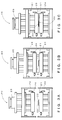
- a laminated body including the metal member 1, the metal porous body 2, and the semiconductor chip 10 placed on top of each other in this order is set in a sintering apparatus as shown in Figs. 3A to 3C .
- Figs. 3A to 3C are drawings indicating a method of forming a joining structure according to the present embodiment.
- a pressing plate 22 for laying up is placed on a lower heating platen 21 of a sintering apparatus 20 and a laminated body 23 is placed thereon.
- a pressing plate 22 is a plate composed of, for example, Teflon (registered trademark), polyimide, and 42 alloy. Pressing plates for laying up may be placed above and below the laminated body 23.
- An inert atmosphere is an atmosphere which is filled with an inactive gas such as nitrogen, or a vacuum atmosphere.
- the laminated body 23 is sandwiched between the lower heating platen 21 and an upper heating platen 26 and heated and baked while applying a pressure with a press cylinder 25.
- the sintering temperature is preferably greater than or equal to 150 °C and less than or equal to 400 °C.
- the pressure during sintering is preferably greater than or equal to 5 MPa and less than or equal to 20 MPa, and the sintering time is preferably greater than 0 (zero) minute and less than 20 minutes.
- the sintering time is preferably less than or equal to 15 minutes, since the shorter the sintering time, the average crystal grain size ds of the outer layer 1b of the metal member 1 can be made smaller than the average crystal grain size di of the inner layer 1c, and also can be made greater than or equal to the average crystal grain size dp of the metal porous body.
- the metal fine particles in the laminated body 23 are sintered, and a metal porous body 2 is formed between the metal member 1 and the semiconductor chip 10.
- Heat treatment may be further performed after having sintered the metal fine particles.
- diffusion joining is accelerated.
- the heat treatment condition is preferably around 300 °C to 500 °C for 30 minutes to one hour.
- the crystal grain size increases as a result of accelerated recrystallization.
- the average crystal grain size ds of the outer layer 1b of the metal member 1 is smaller than the average crystal grain size di of the inner layer 1c, and the average crystal grain size dp of the metal porous body 2 is smaller than or equal to the average crystal grain size ds of the outer layer 1b.
- the metal porous body 2 is formed on one of the main surfaces 1a of the metal member 1, but the metal porous body may be formed on both main surfaces of the metal member 1.
- the joining structure shown in Fig. 4A has a metal member 1, a metal porous body 2 formed on one of the main surfaces of the metal member 1, a semiconductor chip 10 formed on the metal porous body 2, and a metal porous body 3 formed on the other main surface of the metal member 1.
- the metal member 1 has a first outer layer including the main surface on the metal porous body 2 side, and further has a second outer layer including the main surface on the metal porous body 3 side. Further, a first inner layer is formed between the first outer layer and the second outer layer.
- An average crystal grain size ds 12 of the first outer layer of the metal member 1 is smaller than an average crystal grain size di 1 of the first inner layer of the metal member 1, and an average crystal grain size dp 2 of the metal porous body 2 is smaller than or equal to an average crystal grain size ds 12 of the first outer layer of the metal member 1 (dp 2 ⁇ ds 12 ⁇ di 1 ).
- An average crystal grain size ds 13 of the second outer layer of the metal member 1 is smaller than the average crystal grain size di 1 of the first inner layer of the metal member 1 (ds 13 ⁇ di 1 ).
- mechanical processing such as blasting is applied on both main surfaces of the metal member 1. According to the configuration shown in Fig. 4A , occurrence of crack at the joining portion formed on both faces of the metal member 1 can be prevented.
- a joining structure shown in Fig. 4B has a thick copper sheet (metal member) 4, a metal porous body 5 formed on one of the main surfaces of the thick copper sheet 4, and a semiconductor chip 10 formed on the metal porous body 5, and further, on the other main surface of the thick copper sheet 4, a metal porous body 6, a copper sheet 7, a ceramic sheet 8 and a copper sheet 9 are laminated in this order.
- the thick copper sheet 4 has a first outer layer including a main surface on the metal porous body 5 side, and further has a second outer layer including a main surface on the metal porous body 6 side. Further, a first inner layer is formed between the first outer layer and the second outer layer.
- An average crystal grain size ds 45 of the first outer layer of the thick copper sheet 4 is smaller than an average crystal grain size di 4 of the first inner layer of the thick copper sheet 4, and an average crystal grain size dp 5 of the metal porous body 5 is smaller than or equal to an average crystal grain size ds 45 of the first outer layer (dp 5 ⁇ ds 45 ⁇ di 4 ).
- An average crystal grain size ds 46 of the second outer layer of the thick copper sheet 4 is smaller than an average crystal grain size di 4 of the first inner layer of the thick copper sheet 4, and an average crystal grain size dp 6 of the metal porous body 6 is smaller than or equal to an average crystal grain size ds 46 of the second outer layer of the thick copper sheet 4 (dp 6 ⁇ ds 46 ⁇ di 4 ).
- the copper sheet 7 has a third outer layer including a main surface on the metal porous body 6 side, and a third inner layer formed at a position farther from the metal porous body 6 than the third outer layer in a thickness direction and on the ceramic sheet 8 side.
- An average crystal grain size ds 76 of the third outer layer of the copper sheet 7 is smaller than an average crystal grain size di 7 of the third inner layer of the copper sheet 7, and an average crystal grain size dp 6 of the metal porous body 6 is smaller than or equal to the average crystal grain size ds 76 of the third outer layer of the copper sheet 7 (dp 6 ⁇ ds 76 ⁇ di 7 ).
- an electrode layer may be provided between the metal porous body 2, 5 and the semiconductor chip 10.
- the electrode layer is composed of one or more of Au, Ag, Cu, Pd, and Pt.
- a semiconductor chip has a size of 7 mm x 7 mm and a thickness of 230 ⁇ m, and its joining face is metalized with Ni-Ti-Au alloy.
- the material is SiC.
- Copper fine particle dispersion A copper fine particle dispersion in which copper fine particles are dispersed in diethylene glycol at a Cu concentration of 80 mass% was used.
- the copper fine particle dispersion contains 0.3 mass% polyvinylpyrrolidone blended therein as a high polymer dispersing agent.
- Silver fine particle dispersion A silver fine particle dispersion in which silver fine particles are dispersed in octanediol at an Ag concentration of 89 mass% (silver nano paste manufactured by DOWA METALTECH CO., LTD.) was used.
- DBC substrate (Cu/Al 2 O 3 (alumina) /Cu) manufactured by NIPPON STEEL & SUMIKIN Electronics Devices Inc., was used. It has Cu sheet thickness 0.3 mm/ceramic sheet thickness 0.32 mm/Cu sheet thickness 0.3 mm.
- Ni ⁇ Cr/Cu (0.2 ⁇ m/6 ⁇ m) was deposited onto a white ceramic substrate of Al 2 O 3 (alumina) having a thickness of 0.64 mm, and thereafter, thickened under the following plating condition until Cu has a thickness 0.3 mmt for both faces.
- Oxygen-free copper C1020 was used. Thickness was 1.2 mm.
- DBC substrate (Cu/Al 2 O 3 (alumina)/Cu) manufactured by NIPPON STEEL & SUMIKIN Electronics Devices Inc., was used. It was Cu sheet thickness: 0.3 mm/ceramic sheet thickness: 0.32 mm/Cu sheet thickness 0.3 mm.
- One of the surfaces of one copper sheet 7 of the DBC substrate was cleaned, and thereafter, processed by a wet blast (WB) method using a medium of alumina beads having a particle diameter of 40 ⁇ m with a pressure of 0.20 MPa and a processing speed of 10 mm/sec. Then, a copper fine particle dispersion was applied to a WB-processed surface such that the dispersion has a thickness of 100 ⁇ m, and dried at 110 °C for 15 minutes. Further, a thick copper sheet 4 having a thickness of 0.3 mm was mounted on a copper fine particle dispersion layer obtained by the drying process, and set in a sintering apparatus.
- WB wet blast
- Sintering was performed under a reduced pressure atmosphere (oxygen concentration less than or equal to 1,000 ppm), at 300 °C, under a pressure of 10 MPa for 15 minutes to form a metal porous body 6 between the thick copper sheet 4 and the copper sheet 7 of the DBC substrate.
- DBC substrate (Cu/Al 2 O 3 (alumina)/Cu) manufactured by NIPPON STEEL & SUMIKIN Electronics Devices Inc., was used. It was Cu sheet thickness: 0.3 mm/ceramic sheet thickness: 0.32 mm/Cu sheet thickness 0.3 mm.
- a copper foil having a thickness of 0.1 mm was heat-treated at 500 °C for one hour, and thereafter, a plating layer having a thickness of 0.1 mm was formed on both surfaces of the copper foil under plating conditions described below to form a thick copper sheet 4.
- One of the surfaces of the copper sheet 7 of the DBC substrate was cleaned, and thereafter, processed by a wet blast (WB) method using a medium of alumina beads having a particle diameter of 40 ⁇ m with a pressure of 0.20 MPa and a processing speed of 10 mm/sec. Then, a copper fine particle dispersion was applied to a WB-processed surface such that the dispersion has a thickness of 100 ⁇ m, and dried at 110 °C for 15 minutes. Further, the copper foil with plating layer obtained by forming a plating layer on both surfaces of the copper foil was mounted on a copper fine particle dispersion layer obtained by the drying process and set in a sintering apparatus.
- WB wet blast
- a sample was fabricated which includes a porous body and a semiconductor chip formed on a metal member, and ground on its semiconductor chip side until about 10 ⁇ m of the semiconductor chip is remaining. Thereafter, it is processed by Ga beam etching using a nano-processing microscope system (FIB apparatus; Manufactured by SII Nano Technology Corporation SMI3050TB) until the thickness is 50 nm, and a sample is cut out by cutting with a microprobe.
- This sample was set in TEM (JEM3010 manufactured by JEOL), a TEM image was obtained under the conditions of an acceleration voltage of 200 KV and a magnification of x5,000 for observing the crystal grain size of the metal porous body.
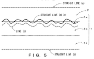
- a straight line (a) was drawn in the middle of the thickness direction of the metal porous body using a software accompanying the TEM (JEM3010 manufactured by JEOL), and an average value of (length + breadth)/2 for twenty crystals existing on the straight line (a) was calculated.
- the straight line (a) was drawn as follows.
- a sample was fabricated which includes a metal porous body and a semiconductor chip that are formed on a metal member.
- the sample was subjected to a thermal cycle test (a cycling test in which 150 °C is maintained for 30 minutes and thereafter -40 °C is maintained for 30 minutes), and observed with an ultra-sonic testing machine (SAT) every 100 cycles.
- SAT ultra-sonic testing machine
- an ultrasonic wave was irradiated from the semiconductor device side, and adjusted by a gate such that it enters from a reverse face of the semiconductor device to the front face of the metal member surface by a reflection method, and measurement was carried out to check whether there are any defects such as peeling or a void in the joining face or in the metal porous body.
- the test was repeated until peeling was observed in an area of greater than or equal to 10% of the area of a joining face between the metal member and the metal porous body. An average value for twenty samples was calculated for the number of cycles before peeling.
- an average number of cycles of greater than or equal to 1000 was defined as “acceptable”, and less than 1000 was defined as “not acceptable”.
- an average number of cycles of greater than or equal to 500 was defined as “acceptable”, and less than 500 was defined as “not acceptable”.
- a surface of a copper sheet of a DBC substrate was cleaned, and thereafter, processed by a wet blast (WB) method using a medium of alumina beads having a particle diameter of 14 ⁇ m with a pressure of 0.20 MPa and a processing speed of 20 mm/sec. Then, a copper fine particle dispersion was applied to have a thickness of 100 ⁇ m, and dried at 110 °C for 15 minutes. After mounting a semiconductor chip, it was set in a sintering apparatus. Sintering was performed under a reduced pressure atmosphere (oxygen concentration less than or equal to 1,000 ppm), at 300 °C, under a pressure of 10 MPa for 15 minutes.
- WB wet blast
- Example 1-1 It was carried out with a method similar to Example 1-1, except that a further heat-treatment was performed after sintering.
- the heat treatment was performed at 500 °C for 30 minutes.
- Example 1-1 It was carried out with a method similar to Example 1-1, except that conditions of a surface treatment was changed.
- the surface treatment was, specifically, performed by a wet blast (WB) method using a medium of alumina beads having a particle diameter of 40 ⁇ m with a pressure of 0.20 MPa and a processing speed of 10 mm/sec.
- WB wet blast
- Example 1-2 It was carried out with a method similar to Example 1-2, except that a substrate obtained by forming a thin film layer of Ni/Cr/Cu by sputtering and a plating layer on a ceramic plate, in place of a DBC substrate, was used, and a heat treatment was performed before a surface treatment. The heat treatment was performed at 400 °C for 30 minutes.
- Example 1-3 It was carried out with a method similar to Example 1-3, except that a further heat treatment was performed after sintering.
- the heat treatment was performed at 500 °C for 30 minutes.
- the surface treatment was, specifically, performed by a wet blast (WB) method using a medium of alumina beads having a particle diameter of 7 ⁇ m with a pressure of 0.2 MPa and a processing speed of 20 mm/sec.
- WB wet blast
- Example 1-1 It was carried out with a method similar to Example 1-1, except that conditions of a surface treatment was changed.
- the surface treatment was, specifically, performed by a wet blast (WB) method using a medium of alumina beads having a particle diameter of 7 ⁇ m with a pressure of 0.2 MPa and a processing speed of 20 mm/sec.
- WB wet blast
- Example 1-1 It was carried out with a method similar to Example 1-1, except that the DBC substrate was replaced with a substrate obtained by forming a thin film layer of Ni/Cr/Cu by sputtering and a plating layer on a ceramic plate.
- Example 1-2 It was carried out with a method similar to Example 1-2, except that heat-treatment was carried out before a surface treatment.
- the heat treatment was performed at 400 °C for one hour.
- Example 1-6 It was carried out with a method similar to Example 1-6, except that sintering was performed at 200 °C and heat treatment was further performed after sintering. The heat treatment was performed at 500 °C for 30 minutes.
- Example 1-11 It was carried out with a method similar to Example 1-11, except that conditions of a surface treatment was changed and sintering was performed at 200 °C.
- the surface treatment was, specifically, performed by a wet blast (WB) method using a medium of alumina beads having a particle diameter of 40 ⁇ m with a pressure of 0.2 MPa and a processing speed of 20 mm/sec.
- WB wet blast
- Example 1-1 It was carried out with a method similar to Example 1-1, except that the surface treatment was changed from a WB process to plasma treatment. Specifically, first, a DBC substrate was set in a chamber of a spattering apparatus and evacuated. Then, Ar gas was introduced into the chamber and the pressure inside the chamber was set at 1 Pa. By supplying electric power using a RF source, Ar plasma was produced near the copper sheet surface of the DBC substrate and irradiated on a copper sheet surface. The condition of an input power of this RF source was 0.25 W/cm 2 and irradiation time was five minutes.
- Example 1-10 It was carried out with a method similar to Example 1-10, except that heat treatment was further performed after sintering. The heat treatment was performed at 500 °C for 30 minutes.
- Example 2-1 It was carried out with a method similar to Example 2-1, except that the surface treatment was changed from a WB process to plasma treatment.
- the plasma treatment was performed by a method similar to Comparative Example 1-2.
- a thick copper sheet laminated DBC substrate including a thick copper sheet (metal member) connected to a ceramic substrate via a sintered body was used.
- Example 3-1 It was carried out with a method similar to Example 3-1, except that surface treatment was not performed on the ceramic substrate side surface of the thick copper sheet on the metal porous body side of the thick copper sheet laminated DBC substrate, and that surface treatment was performed only on the semiconductor chip side surface of the thick copper sheet.
- an average number of cycles in TCT was greater than or equal to 1000 for each of Examples 1-1 to 1-16, and it can be seen that crack occurrence preventing property was good.
- an average number of cycles in TCT was greater than or equal to 1500 for each of Examples 1-1 to 1-9, and thus it can be seen that crack occurrence preventing property was particularly excellent.
- an average number of cycles in TCT was 600 and 580, which are small, for Comparative Examples 1-1 and 1-2 in which the crystal grain size of the outer layer and the crystal grain size of the inner layer were the same.
- An average number of cycles in TCT was 510, which is very small, for Comparative Example 1-3 in which the crystal grain size of the outer layer was greater than the crystal grain size of the inner layer.
- an average number of cycles in TCT was greater than or equal to 600 for each of Examples 2-1 to 2-16, and it can be seen that crack occurrence preventing property was good.
- an average number of cycles in TCT was greater than or equal to 650 for each of Examples 2-1 to 2-9, and thus it can be seen that crack occurrence preventing property was particularly excellent.
- an average number of cycles in TCT was 330 and 410, which are small, for Comparative Examples 2-1 and 2-2 in which the crystal grain size of the outer layer and the crystal grain size of the inner layer were the same.
- an average number of cycles in TCT was greater than or equal to 1000 for each of Examples 3-1 to 3-17, and it can be seen that crack occurrence preventing property was good.
- an average number of cycles in TCT was greater than or equal to 2000 for each of Examples 3-1 to 3-16, and thus it can be seen that crack occurrence preventing property was extremely excellent.
- an average number of cycles in TCT was greater than or equal to 1000 for each of Examples 4-1 to 4-16, and it can be seen that crack occurrence preventing property was excellent.
- an average number of cycles in TCT was 590 and 530, which are small, for Comparative Examples 4-1 and 4-2 in which the crystal grain size of the outer layer and the crystal grain size of the inner layer were the same.
- An average number of cycles in TCT was 500, which is very small, for Comparative Example 4-3 in which the crystal grain size of the outer layer was greater than the crystal grain size of the inner layer.
Landscapes
- Chemical & Material Sciences (AREA)
- Engineering & Computer Science (AREA)
- Composite Materials (AREA)
- Manufacturing & Machinery (AREA)
- Materials Engineering (AREA)
- Mechanical Engineering (AREA)
- Die Bonding (AREA)
- Powder Metallurgy (AREA)
Abstract
Description
- The present invention relates to a joining structure and an electronic member-joining structural body wherein a metal porous body is joined to a metal member, and particularly relates to a joining structure where the metal member is a circuit board, a substrate such as a ceramic substrate or a lead frame.
- Solder is generally used for connecting a semiconductor device that controls or supplies power (a so-called power semiconductor device) to a substrate such as a circuit board or a ceramic substrate or to a wiring member such as a lead frame. Commonly-used solder for such a purpose is solder cream, which is made to have suitable viscosity by adding flux to solder powder. However, when flux is used, the surface of the semiconductor device could be contaminated, and there is a problem that a cleaning step becomes necessary. Further, in recent years, considering an environment impact, it is required to use lead-free solder materials that do not contain lead. Au-Sn solder is known as a lead-free solder material which can withstand heat generation by a power semiconductor device, but it is expensive and thus not practical. Sn-Ag-Cu solder is a solder material that is less expensive than Au-Sn solder, but has a problem that a growth of an intermetallic compound due to thermal history may lead to a decrease in reliability.
- As a joining member free of solder, Anisotropic Conductive Film (ACF) is also known that is a film formed of a mixture of a thermosetting resin and fine metal particles having conductivity. However, there is a concern that the thermosetting resin may degrade due to high heat, and thus an ACF is not suitable for connecting power semiconductor devices that produce a large amount of heat.
- As another joining member free of solder, an Ag paste obtained by dispersing Ag particles in a resin has been proposed. When using an Ag paste as a joining member for a power semiconductor device, high thermal conductivity and high electric conductivity are required. Thus, it is necessary to increase the content of Ag in the paste. However, as the content of Ag becomes greater, the ratio of resin which is likely to show elastic deformation becomes smaller. Accordingly, rigidity of the joining layer after the curing process increases, and a strain absorbing capability of the joining layer decreases. When a strain greater than the strain absorbing capability is applied to such joining layer, there is a problem that a defect may occur at a contact interface between an electrode or a die pad of the semiconductor device and Ag particles, and thus peeling may occur.
- Further, in a case where an electrode of the semiconductor device or an electrode of the substrate contains Ni and an Ag paste is used as a joining member, joining strength (adhesiveness) is low, and thus there is a problem that the interface may break due to an external force during handling and a required long-term reliability cannot be achieved. Thus, it is necessary to apply a noble metal plating on an electrode of the semiconductor device or an electrode of the substrate. However, when joining is performed as described above by applying a noble metal plating, a thermal stress on the semiconductor chip due to a difference in thermal expansion between the members increases, and thus there is a problem of a decrease in durability.
- Accordingly, recently, it is known to supply metal particles coated with an organic material and having an average particle diameter of less than or equal to 100 nm between the materials to be joined, and joining them by decomposing the organic material by heating and sintering the metal particles with each other (e.g., Patent Document 1).
- Further, it is proposed to join members to be joined by forming an oxide layer containing oxygen at a joining interface of the members to be joined, disposing a joining material including metal compound particles having an average particle diameter of greater than or equal to 1 nm and less than or equal to 50 µm and a reducing agent composed of an organic material, and heating and applying a pressure between the members to be joined (e.g., Patent Document 2). It is described that, with this configuration, metal compound particles are reduced at a temperature lower than that of the case of heating and decomposing the metal compound particles as a single body, and metal particles having an average particle diameter of less than or equal to 100 nm are produced. Further, it is disclosed that, after having produced an oxide layer on a joining face prior to the joining, an oxidizing process is applied on this layer to produce an oxidized layer having a thickness greater than or equal to a thickness of a naturally oxidized layer, to thereby efficiently perform discharging of an oxide in the joined material during the joining, and thus a shearing strength of the joining face can be increased.
- Also, it is proposed to connect two metal surfaces with each other after having applied a treatment on the two metal surfaces, such that a connection having conductivity can be formed by substitution diffusion between the same metal ions and/or metal atoms. (E.g., Patent Document 3).
-
- [Patent Document 1] Japanese Laid-Open Patent Publication
2004-107728 - [Patent Document 2] Japanese Laid-Open Patent Publication
2008-208442 - [Patent Document 3] Japanese Laid-Open Patent Publication
2013-524494 - With the configurations of
Patent Documents - It is an object of the present invention to provide a joining structure and an electronic member joining structural body that prevents crack initiation at a joining portion between a metal member and a metal porous body, and can achieve a highly reliable joining.
- In order to achieve the above object, a joining structure according to the present invention comprising a metal member and a metal porous body formed on the metal member is characterized in that the metal member includes a first outer layer and a first inner layer, the first outer layer including at least one of main surfaces and being formed on the metal porous body side, the first inner layer being formed at a position farther from the metal porous body than the first outer layer in a thickness direction, the first outer layer has an average crystal grain size ds that is smaller than an average crystal grain size di of the first inner layer, and the metal porous body has an average crystal grain size dp that is smaller than or equal to the average crystal grain size ds of the first outer layer.
- Further, it is preferable that the average crystal grain size ds and the average crystal grain size dp satisfies:

- Further, it is preferable that the average crystal grain size ds is greater than or equal to 0.2 µm and less than 10 µm.
- Further, it is preferable that the average crystal grain size di is greater than or equal to 10 µm and less than 100 µm.
- Further, it is preferable that the average crystal grain size dp is greater than or equal to 0.1 µm and less than or equal to 1 µm.
- Further, it is preferable that the metal member and the metal porous body comprises a metal material that is Cu or Cu alloy or Ag or Ag alloy.
- It is preferable that a metal sheet is further provided on the metal porous body.
- It is preferable that the metal sheet includes a second outer layer and a second inner layer, the second outer layer including at least one of main surfaces and being formed on the metal porous body, the second inner layer being formed at a position farther from the metal porous body than the second outer layer in a thickness direction, and
the second outer layer has an average crystal grain size ds' that is smaller than the average crystal grain size di' of the second inner layer. - It is preferable that the metal member to be substrate for lead frame.
- An electronic member-joining structural body according to the present invention comprising a ceramic substrate, a metal porous body formed on the ceramic substrate, and an electronic member disposed on the metal porous body is characterized in that the ceramic substrate includes a ceramic body and a metal layer formed on the ceramic body, the metal layer includes an outer layer and an inner layer, the outer layer including at least one of main surfaces and being formed on the metal porous body side, the inner layer being formed at a position farther from the metal porous body than the outer layer in a thickness direction, the outer layer has an average crystal grain size ds that is less than an average crystal grain size di of the inner layer, and the metal porous body has an average crystal grain size dp that is smaller than or equal to the average crystal grain size ds of the outer layer.
- It is preferable that an electrode layer including one or more of Au, Ag, Cu, Pd and Pt is provided between the metal porous body and the electronic member.
- According to the joining structure of the present invention, since a yield strain continuously varies in a thickness direction of a laminated body, a strain concentration is suppressed, and thus a crack initiation point is less likely to occur when strain is applied repeatedly. Also, since the crystal grain size of an inner layer of the metal member is large, an overall strain relaxation effect is great. Therefore, crack initiation at a joining portion of a metal member and a metal porous body is prevented, and reliable joining can be achieved.
-
- [
Fig. 1] Fig. 1 is a cross sectional view schematically showing a joining structure according to an embodiment of the present invention. - [
FIG. 2] Fig. 2 is an enlarged cross sectional schematic view of an interface portion of a metal porous body and a metal member for explanation of the joining structure according to an embodiment of the present invention. - [
FIG. 3] Figs. 3A to 3C are diagrams showing a method of forming a joining structure according to an embodiment of the present invention. - [
FIG. 4] Figs. 4A to 4B are cross sectional views of a joining structure according to other embodiments of the present invention. - [
FIG. 5] Fig. 5 is a diagram for explaining a calculation method of a crystal grain size. - Hereinafter, embodiments of the present invention will be described in detail with reference to the attached drawings.
-
Fig. 1 is a cross sectional view schematically showing a joining structure according to the present embodiment. As shown inFig. 1 , the joining structure of the present embodiment includes ametal member 1, and a metalporous body 2 formed on one of main surfaces of themetal member 1. On the metalporous body 2, asemiconductor chip 10 is disposed. - The
metal member 1 is not particularly limited as long as it is a member containing metal, and may be, for example, a substrate such as a circuit board, a lead frame, or a connector member. It is preferable that the metal member is composed of a metal material such as Cu or Cu alloy, or Ag or Ag alloy. A circuit board may be a DBC (Direct Bonding Copper) substrate or an AMC (Active-metal brazed copper) substrate wherein a copper sheet is joined to a ceramic substrate. Alumina (Al2O3) may be used as a ceramic of a DBC substrate, and silicon nitride (Si3N4) or aluminum nitride (AIN) may be used as a ceramic of an AMC substrate. - The metal
porous body 2 is formed by sintering a metal fine particle dispersion containing metal fine particles and an organic dispersion medium. It is preferable that the metal fine particles are: fine particles composed of one of metals selected from a group of metal elements consisting of Cu, Ag, Au, Al, Ni, Pt, Sn, Sb and Pd; fine particles which are a mixture of two or more metals selected from the aforementioned group of metal elements; fine particles composed of an alloy of two or more elements selected from the aforementioned group of metal elements; fine particles which are a mixture of fine particles of one element selected from the aforementioned group of metal elements or fine particles of a mixture of two or more elements selected from the aforementioned group of metal elements and fine particles composed of an alloy of two or more elements selected from the aforementioned group of metal elements. Also, the metal fine particles may be fine particles composed of an oxide of the aforementioned metals or fine particles composed of an oxide of the aforementioned alloy, or the oxide may be a part of the fine particles. - It is preferable that an average particle diameter (average particle diameter of primary particles) of the metal fine particles is greater than or equal to 5 nm and less than or equal to 200 nm. As used herein, "an average particle diameter of the primary particles" means an average of the diameters of the primary particles which are individual metal fine particles constituting a secondary particle. A primary particle size can be measured using an electron microscope. Also, the average particle diameter means a number average particle size of the primary particles. With the average particle diameter of the metal fine particle being greater than or equal to 5 nm, a metal porous body having a homogeneous crystal grain size and pores after baking can be obtained.
- The organic dispersion medium is preferably polyalcohol, and more preferably, one or two or more polyol having two or more hydroxyl groups in a molecule. Specifically, polyol may be one or two or more selected from ethylene glycol, diethylene glycol, 1,2-propanediol, 1,3-propanediol, 1,2-butanediol, 1,3-butanediol, 1,4-butanediol, 2-butene-1,4-diol, 1,2,6-hexantriol, glycerin, and 2-methyl-2,4-pentanediol.
- The metal fine particle dispersion may contain a dispersion aid substance and/or solvent as appropriate. As a dispersion aid substance, a known substance may be used as appropriate, and considering improvements in dispersibility and sinterability of the metal fine particles, it is desirable to use compounds having an amide group, amine compound, etc.
-
Fig. 2 is an enlarged cross sectional schematic view for explanation of the joining structure according to an embodiment of the present invention. As shown inFig. 2 , themetal member 1 has an outer layer 1b including one of the main surfaces 1a and formed on the metalporous body 2 side, and an inner layer 1c formed at a position (including the other main surface) farther from the metalporous body 2 than the outer layer 1b in a thickness direction. InFig. 2 , the boundary between the outer layer 1b and the inner layer 1c is indicated by a broken line, but this is for the sake of ease of explanation, and in practice, a certain unevenness is formed at the boundary. An average crystal grain size ds of the outer layer 1b is smaller than an average crystal grain size di of the inner layer 1c, and an average crystal grain size dp of the metalporous body 2 is smaller than or equal to an average crystal grain size ds of the outer layer 1b (dp ≤ ds < di). It is preferable that the average crystal grain size ds and the average crystal grain size dp satisfy the following equation:
porous body 2 is smaller than or equal to the average crystal grain size ds of the outer layer 1b, a yield strain continuously varies and thus a strain concentration is suppressed, and a crack initiation point is less likely to occur when strain is applied repeatedly. Also, since the average crystal grain size di of inner layer 1c is large, an overall strain relaxation effect is great. Also, with ds/dp < 100, the average crystal grain size dp of the metalporous body 2 does not become excessively smaller than the average crystal grain size ds of the outer layer 1b, and the yield strain is likely to vary continuously, a strain concentration is suppressed, and the crack initiation point is less likely to occur when strain is applied repeatedly. - It is preferable that the outer layer 1b has an average crystal grain size ds of greater than or equal to 0.2 µm and less than 10 µm. With the average crystal grain size ds of less than 0.2 µm, the yield strain is large, and thus the stress concentrates at an interface (main surface 1a) between the metal
porous body 2 and the outer layer 1b, and a crack is likely to occur. On the other hand, with the average crystal grain size ds that is greater than or equal to 10 µm, the average crystal grain size ds of the outer layer 1b is excessively greater than the average crystal grain size dp of the metalporous body 2, and thus a continuous yield strain is not obtained at the interface between the metalporous body 2 and the outer layer 1b, and a crack is likely to occur when strain is applied repeatedly. It is preferable that the outer layer 1b has a thickness of greater than or equal to 0.5 µm and less than or equal to 10 µm, but should not be limited thereto. - It is preferable that the inner layer 1c has an average crystal grain size di of greater than or equal to 10 µm and less than or equal to 100 µm. In a case where the average crystal grain size di of less than 10 µm, an overall distortion relaxation effect of the metal
porous body 2 and themetal member 1 becomes small. On the other hand, in a case where the average crystal grain size di being greater than or equal to 100 µm, the average crystal grain size di of the inner layer 1c becomes excessively greater than the average crystal grain size ds of the outer layer 1b, and a continuous yield strain is not obtained in themetal member 1, and a crack is likely to occur when strain is applied repeatedly. - It is preferable that the average crystal grain size dp of the metal
porous body 2 is greater than or equal to 1 µm and less than or equal to 0.1 µm. In a case where the average crystal grain size dp of less than 0.1 µm, sintering of the metalporous body 2 will be insufficient, and the bonding between the metal particles is likely to be weak. On the other hand, in a case where the average crystal grain size dp of greater than 1 µm, since metal diffusion of the metal fine particles has progressed, microvoids in the metalporous body 2 decreases and the rigidity of the metalporous body 2 as a whole increases. Thus, a stress load on an electronic member (e.g., semiconductor chip), which is an object to be connected, increases. In a case where the metal material composing the metalporous body 2 is Ag or Ag alloy, the average crystal grain size dp of the metalporous body 2 may be greater than 1 µm. - A method of joining the
semiconductor chip 10 with themetal member 1 via the metalporous body 2 will now be described. - First, a process of forming the outer layer 1b at the main surface 1a of the
metal member 1 is performed. By forming the outer layer 1b, atomic vacancy and/or inversion is produced at a surface of themetal member 1, and it is preferably carried out by mechanical processing such as grinding by blasting or buffing. In the case of the grinding by blasting, an abrasive material may be glass beads, alumina beads, and zirconia beads. The shape of the abrasive material may be spherical or polygonal, but should not be limited thereto. - The thickness of outer layer 1b is preferably greater than or equal to 0.5 µm and less than or equal to 10 µm, but should not be limited thereto. The surface roughness Ra of the outer layer 1b is preferably greater than or equal to 0.1 µm and less than or equal to 2.0 µm, but should not be limited thereto.
- Further, a thermal treatment may be performed prior to the process of forming the outer layer 1b on the main surface 1a of the
metal member 1. By performing a thermal treatment, recrystallization of themetal member 1 is accelerated, and the crystal grain size can be increased. Considering the recrystallization, the thermal treatment condition is preferably about 300 °C to 400 °C for less than or equal to 1 hour. - Then, metal fine particle dispersion is applied to the
metal member 1 and predrying is performed by heating at 100 °C to 150 °C for 5 to 20 minutes. Asemiconductor chip 10 is placed on a metal member on which metal fine particles is placed. Then, a laminated body including themetal member 1, the metalporous body 2, and thesemiconductor chip 10 placed on top of each other in this order is set in a sintering apparatus as shown inFigs. 3A to 3C . -
Figs. 3A to 3C are drawings indicating a method of forming a joining structure according to the present embodiment. As shown inFig. 3A , apressing plate 22 for laying up is placed on alower heating platen 21 of asintering apparatus 20 and alaminated body 23 is placed thereon. Apressing plate 22 is a plate composed of, for example, Teflon (registered trademark), polyimide, and 42 alloy. Pressing plates for laying up may be placed above and below thelaminated body 23. - Then, a
chamber 24 is closed, and an inert atmosphere is created in the chamber 24 (Fig. 3B ). An inert atmosphere is an atmosphere which is filled with an inactive gas such as nitrogen, or a vacuum atmosphere. By creating an inert atmosphere in thechamber 24, it is possible to remove an oxidization layer on a surface of metal fine particles and sinterability of the metal fine particles can be improved. - Then, as shown in
Fig. 3C , thelaminated body 23 is sandwiched between thelower heating platen 21 and anupper heating platen 26 and heated and baked while applying a pressure with apress cylinder 25. The sintering temperature is preferably greater than or equal to 150 °C and less than or equal to 400 °C. The pressure during sintering is preferably greater than or equal to 5 MPa and less than or equal to 20 MPa, and the sintering time is preferably greater than 0 (zero) minute and less than 20 minutes. The sintering time is preferably less than or equal to 15 minutes, since the shorter the sintering time, the average crystal grain size ds of the outer layer 1b of themetal member 1 can be made smaller than the average crystal grain size di of the inner layer 1c, and also can be made greater than or equal to the average crystal grain size dp of the metal porous body. By this baking, the metal fine particles in thelaminated body 23 are sintered, and a metalporous body 2 is formed between themetal member 1 and thesemiconductor chip 10. - Heat treatment may be further performed after having sintered the metal fine particles. By performing heat treatment, diffusion joining is accelerated. To obtain sufficient diffusion joining, the heat treatment condition is preferably around 300 °C to 500 °C for 30 minutes to one hour. The crystal grain size increases as a result of accelerated recrystallization.
- As set forth above, according to the joining structure of the present embodiment, the average crystal grain size ds of the outer layer 1b of the metal member 1is smaller than the average crystal grain size di of the inner layer 1c, and the average crystal grain size dp of the metal
porous body 2 is smaller than or equal to the average crystal grain size ds of the outer layer 1b. Thereby, since yield strain continuously varies in the thickness direction of the joining, a strain concentration is suppressed, and a crack initiation point is less likely to occur when strain is applied repeatedly. Also, since the crystal grain size of the inner layer of themetal member 1 is large, an overall strain relaxation effect is large. Particularly, it is possible to prevent propagation of a crack formed laterally along an interface between themetal member 1 and the metalporous body 2. - In the present embodiment, the metal
porous body 2 is formed on one of the main surfaces 1a of themetal member 1, but the metal porous body may be formed on both main surfaces of themetal member 1. - For example, the joining structure shown in
Fig. 4A has ametal member 1, a metalporous body 2 formed on one of the main surfaces of themetal member 1, asemiconductor chip 10 formed on the metalporous body 2, and a metal porous body 3 formed on the other main surface of themetal member 1. Themetal member 1 has a first outer layer including the main surface on the metalporous body 2 side, and further has a second outer layer including the main surface on the metal porous body 3 side. Further, a first inner layer is formed between the first outer layer and the second outer layer. An average crystal grain size ds12 of the first outer layer of themetal member 1 is smaller than an average crystal grain size di1 of the first inner layer of themetal member 1, and an average crystal grain size dp2 of the metalporous body 2 is smaller than or equal to an average crystal grain size ds12 of the first outer layer of the metal member 1 (dp2 ≤ ds12 < di1). An average crystal grain size ds13 of the second outer layer of themetal member 1 is smaller than the average crystal grain size di1 of the first inner layer of the metal member 1 (ds13 < di1). In this case, mechanical processing such as blasting is applied on both main surfaces of themetal member 1. According to the configuration shown inFig. 4A , occurrence of crack at the joining portion formed on both faces of themetal member 1 can be prevented. - A joining structure shown in
Fig. 4B has a thick copper sheet (metal member) 4, a metalporous body 5 formed on one of the main surfaces of thethick copper sheet 4, and asemiconductor chip 10 formed on the metalporous body 5, and further, on the other main surface of thethick copper sheet 4, a metalporous body 6, acopper sheet 7, aceramic sheet 8 and acopper sheet 9 are laminated in this order. Thethick copper sheet 4 has a first outer layer including a main surface on the metalporous body 5 side, and further has a second outer layer including a main surface on the metalporous body 6 side. Further, a first inner layer is formed between the first outer layer and the second outer layer. An average crystal grain size ds45 of the first outer layer of thethick copper sheet 4 is smaller than an average crystal grain size di4 of the first inner layer of thethick copper sheet 4, and an average crystal grain size dp5 of the metalporous body 5 is smaller than or equal to an average crystal grain size ds45 of the first outer layer (dp5 ≤ ds45 < di4). An average crystal grain size ds46 of the second outer layer of thethick copper sheet 4 is smaller than an average crystal grain size di4 of the first inner layer of thethick copper sheet 4, and an average crystal grain size dp6 of the metalporous body 6 is smaller than or equal to an average crystal grain size ds46 of the second outer layer of the thick copper sheet 4 (dp6 ≤ ds46 < di4). - Further, the
copper sheet 7 has a third outer layer including a main surface on the metalporous body 6 side, and a third inner layer formed at a position farther from the metalporous body 6 than the third outer layer in a thickness direction and on theceramic sheet 8 side. An average crystal grain size ds76 of the third outer layer of thecopper sheet 7 is smaller than an average crystal grain size di7 of the third inner layer of thecopper sheet 7, and an average crystal grain size dp6 of the metalporous body 6 is smaller than or equal to the average crystal grain size ds76 of the third outer layer of the copper sheet 7 (dp6 ≤ ds76 < di7). In this case, mechanical processing such as blasting is applied on the metalporous body 6 side main surface and the metalporous body 5 side main surface (both faces) of thethick copper sheet 4 and on the metalporous body 6 side main surface of thecopper sheet 7. According to the configuration ofFig. 4B , occurrence of a crack can be suppressed not only at the joining portion formed on one of the faces of the metalporous body 5, but also at the joining portions formed on both faces of metalporous body 6. - Note that, an electrode layer, not shown, may be provided between the metal
porous body semiconductor chip 10. For example, the electrode layer is composed of one or more of Au, Ag, Cu, Pd, and Pt. - Hereinafter, preferred embodiments of the present invention will be described in detail based on examples and comparative examples, but the present invention is not limited to these examples.
- Hereinafter, (1) raw materials, (2) an apparatus, and (3) an evaluation method used for Examples and Comparative Examples will be described.
- A semiconductor chip has a size of 7 mm x 7 mm and a thickness of 230 µm, and its joining face is metalized with Ni-Ti-Au alloy. The material is SiC.
- Copper fine particle dispersion: A copper fine particle dispersion in which copper fine particles are dispersed in diethylene glycol at a Cu concentration of 80 mass% was used. The copper fine particle dispersion contains 0.3 mass% polyvinylpyrrolidone blended therein as a high polymer dispersing agent.
- Silver fine particle dispersion: A silver fine particle dispersion in which silver fine particles are dispersed in octanediol at an Ag concentration of 89 mass% (silver nano paste manufactured by DOWA METALTECH CO., LTD.) was used.
- DBC substrate (Cu/Al2O3 (alumina) /Cu) manufactured by NIPPON STEEL & SUMIKIN Electronics Devices Inc., was used. It has Cu sheet thickness 0.3 mm/ceramic sheet thickness 0.32 mm/Cu sheet thickness 0.3 mm.
- Ni·Cr/Cu (0.2 µm/6 µm) was deposited onto a white ceramic substrate of Al2O3 (alumina) having a thickness of 0.64 mm, and thereafter, thickened under the following plating condition until Cu has a thickness 0.3 mmt for both faces.
- Plating Solution: CuSO4·5H2O 250 g/L (water), H2SO4 50 g/L (water), NaCl 0.1 g/L (water)
- Electric current density: 5A/dm2, temperature 40 °C
- Oxygen-free copper C1020 was used. Thickness was 1.2 mm.
- DBC substrate (Cu/Al2O3 (alumina)/Cu) manufactured by NIPPON STEEL & SUMIKIN Electronics Devices Inc., was used. It was Cu sheet thickness: 0.3 mm/ceramic sheet thickness: 0.32 mm/Cu sheet thickness 0.3 mm.
- One of the surfaces of one
copper sheet 7 of the DBC substrate was cleaned, and thereafter, processed by a wet blast (WB) method using a medium of alumina beads having a particle diameter of 40 µm with a pressure of 0.20 MPa and a processing speed of 10 mm/sec. Then, a copper fine particle dispersion was applied to a WB-processed surface such that the dispersion has a thickness of 100 µm, and dried at 110 °C for 15 minutes. Further, athick copper sheet 4 having a thickness of 0.3 mm was mounted on a copper fine particle dispersion layer obtained by the drying process, and set in a sintering apparatus. Sintering was performed under a reduced pressure atmosphere (oxygen concentration less than or equal to 1,000 ppm), at 300 °C, under a pressure of 10 MPa for 15 minutes to form a metalporous body 6 between thethick copper sheet 4 and thecopper sheet 7 of the DBC substrate. - DBC substrate (Cu/Al2O3 (alumina)/Cu) manufactured by NIPPON STEEL & SUMIKIN Electronics Devices Inc., was used. It was Cu sheet thickness: 0.3 mm/ceramic sheet thickness: 0.32 mm/Cu sheet thickness 0.3 mm.
- A copper foil having a thickness of 0.1 mm was heat-treated at 500 °C for one hour, and thereafter, a plating layer having a thickness of 0.1 mm was formed on both surfaces of the copper foil under plating conditions described below to form a
thick copper sheet 4. - One of the surfaces of the
copper sheet 7 of the DBC substrate was cleaned, and thereafter, processed by a wet blast (WB) method using a medium of alumina beads having a particle diameter of 40 µm with a pressure of 0.20 MPa and a processing speed of 10 mm/sec. Then, a copper fine particle dispersion was applied to a WB-processed surface such that the dispersion has a thickness of 100 µm, and dried at 110 °C for 15 minutes. Further, the copper foil with plating layer obtained by forming a plating layer on both surfaces of the copper foil was mounted on a copper fine particle dispersion layer obtained by the drying process and set in a sintering apparatus. Sintering was performed under a reduced pressure atmosphere (oxygen concentration less than or equal to 1,000 ppm), at 300 °C, under a pressure of 10 MPa for 15 minutes to form a metalporous body 6 between thethick copper sheet 4 and thecopper sheet 7 of the DBC substrate. Plating solution: CuSO4·5H2O 250 g/L (water), H2SO4 50 g/L (water), NaCl 0.1 g/L (water) - Electric current density: 5A/dm2, temperature 40 °C
- A sintering apparatus shown in
Figs. 3A to 3C was used. - It was measured with a laser microscope (KEYENCE VK9710).
- A sample was fabricated which includes a porous body and a semiconductor chip formed on a metal member, and ground on its semiconductor chip side until about 10 µm of the semiconductor chip is remaining. Thereafter, it is processed by Ga beam etching using a nano-processing microscope system (FIB apparatus; Manufactured by SII Nano Technology Corporation SMI3050TB) until the thickness is 50 nm, and a sample is cut out by cutting with a microprobe. This sample was set in TEM (JEM3010 manufactured by JEOL), a TEM image was obtained under the conditions of an acceleration voltage of 200 KV and a magnification of x5,000 for observing the crystal grain size of the metal porous body. In a TEM image, a straight line (a) was drawn in the middle of the thickness direction of the metal porous body using a software accompanying the TEM (JEM3010 manufactured by JEOL), and an average value of (length + breadth)/2 for twenty crystals existing on the straight line (a) was calculated. The straight line (a) was drawn as follows.
- First, at an interface between the metal substrate and the metal porous body, two points were selected such that a straight line distance between them corresponds to the thickness of the metal porous body, and a straight line (b) connecting the two points was drawn. Then, at a position spaced apart by half the thickness of the metal porous body from the straight line (b) in a thickness direction of the metal porous body, a straight line (a) which is a straight line parallel to the straight line (b) was drawn (
Fig. 5 ). - Using a TEM under the same conditions as in (B), a sample obtained similarly to (B) was used for observing the crystal grain size of the outer layer of the metal member. In a TEM image, at a position at a distance of 1 µm from an interface between the metal porous body and the metal member to the metal member side, a line (c) was drawn along the interface. An average value of (length + breadth)/2 for twenty crystals existing on the line (c) was calculated (
Fig. 5 ). - Using a TEM under the same conditions as in (B), a sample obtained similarly to (B) was used for observing the crystal grain size of the inner layer of the metal member. In a TEM image, a straight line (d) was drawn in the middle in the thickness direction of the metal member. An average value of (length + breadth)/2 for twenty crystals existing on the straight line (d) was calculated. The straight line (d) was drawn as follows.
- First, at an interface between the metal substrate and the metal porous body, two points were selected such that a straight line distance between them corresponds to the thickness of the metal member, and a straight line (e) connecting the two points was drawn. Then, at a position spaced apart by half the thickness of the metal member from the straight line (e) in a thickness direction of the metal member, a straight line (d) which is a straight line parallel to the straight line (e) was drawn (
Fig. 5 ). - A sample was fabricated which includes a metal porous body and a semiconductor chip that are formed on a metal member. The sample was subjected to a thermal cycle test (a cycling test in which 150 °C is maintained for 30 minutes and thereafter -40 °C is maintained for 30 minutes), and observed with an ultra-sonic testing machine (SAT) every 100 cycles. Using an ultra-sonic testing machine (manufactured by Hitachi Construction Machinery Co., Ltd., Mi-Scope) and a probe (model PQ2-13, 50MHz), an ultrasonic wave was irradiated from the semiconductor device side, and adjusted by a gate such that it enters from a reverse face of the semiconductor device to the front face of the metal member surface by a reflection method, and measurement was carried out to check whether there are any defects such as peeling or a void in the joining face or in the metal porous body. The test was repeated until peeling was observed in an area of greater than or equal to 10% of the area of a joining face between the metal member and the metal porous body. An average value for twenty samples was calculated for the number of cycles before peeling.
- For metal members having a ceramic substrate, an average number of cycles of greater than or equal to 1000 was defined as "acceptable", and less than 1000 was defined as "not acceptable". For metal members that is a lead frame material, an average number of cycles of greater than or equal to 500 was defined as "acceptable", and less than 500 was defined as "not acceptable".
- A surface of a copper sheet of a DBC substrate was cleaned, and thereafter, processed by a wet blast (WB) method using a medium of alumina beads having a particle diameter of 14 µm with a pressure of 0.20 MPa and a processing speed of 20 mm/sec. Then, a copper fine particle dispersion was applied to have a thickness of 100 µm, and dried at 110 °C for 15 minutes. After mounting a semiconductor chip, it was set in a sintering apparatus. Sintering was performed under a reduced pressure atmosphere (oxygen concentration less than or equal to 1,000 ppm), at 300 °C, under a pressure of 10 MPa for 15 minutes.
- It was carried out with a method similar to Example 1-1, except that a further heat-treatment was performed after sintering. The heat treatment was performed at 500 °C for 30 minutes.
- It was carried out with a method similar to Example 1-1, except that conditions of a surface treatment was changed. The surface treatment was, specifically, performed by a wet blast (WB) method using a medium of alumina beads having a particle diameter of 40 µm with a pressure of 0.20 MPa and a processing speed of 10 mm/sec.
- It was carried out with a method similar to Example 1-2, except that a substrate obtained by forming a thin film layer of Ni/Cr/Cu by sputtering and a plating layer on a ceramic plate, in place of a DBC substrate, was used, and a heat treatment was performed before a surface treatment. The heat treatment was performed at 400 °C for 30 minutes.
- It was carried out with a method similar to Example 1-3, except that a further heat treatment was performed after sintering. The heat treatment was performed at 500 °C for 30 minutes.
- It was carried out with a method similar to Example 1-4, except that conditions of a surface treatment was changed and a further heat treatment was not carried out after sintering. The surface treatment was, specifically, performed by a wet blast (WB) method using a medium of alumina beads having a particle diameter of 7 µm with a pressure of 0.2 MPa and a processing speed of 20 mm/sec.
- It was carried out with a method similar to Example 1-1, except that conditions of a surface treatment was changed. The surface treatment was, specifically, performed by a wet blast (WB) method using a medium of alumina beads having a particle diameter of 7 µm with a pressure of 0.2 MPa and a processing speed of 20 mm/sec.
- It was carried out with a method similar to Example 1-4, except that heat treatment before a surface treatment was performed at 400 °C for 15 minutes.
- It was carried out with a method similar to Example 1-1, except that the DBC substrate was replaced with a substrate obtained by forming a thin film layer of Ni/Cr/Cu by sputtering and a plating layer on a ceramic plate.
- It was carried out with a method similar to Example 1-1, except that sintering was performed at 250 °C.
- It was carried out with a method similar to Example 1-2, except that heat-treatment was carried out before a surface treatment. The heat treatment was performed at 400 °C for one hour.
- It was carried out with a method similar to Example 1-3, except that heat-treated was further performed after sintering. The heat treatment was performed at 500 °C for 30 minutes.
- It was carried out with a method similar to Example 1-6, except that sintering was performed at 200 °C and heat treatment was further performed after sintering. The heat treatment was performed at 500 °C for 30 minutes.
- It was carried out with a method similar to Example 1-12, except that sintering was performed at 200 °C.
- It was carried out with a method similar to Example 1-13, except that heat treatment was not performed before a surface treatment and sintering was performed at 250 °C.
- It was carried out with a method similar to Example 1-11, except that conditions of a surface treatment was changed and sintering was performed at 200 °C. The surface treatment was, specifically, performed by a wet blast (WB) method using a medium of alumina beads having a particle diameter of 40 µm with a pressure of 0.2 MPa and a processing speed of 20 mm/sec.
- It was carried out with a method similar to Example 1-1, except that a surface treatment was not performed.
- It was carried out with a method similar to Example 1-1, except that the surface treatment was changed from a WB process to plasma treatment. Specifically, first, a DBC substrate was set in a chamber of a spattering apparatus and evacuated. Then, Ar gas was introduced into the chamber and the pressure inside the chamber was set at 1 Pa. By supplying electric power using a RF source, Ar plasma was produced near the copper sheet surface of the DBC substrate and irradiated on a copper sheet surface. The condition of an input power of this RF source was 0.25 W/cm2 and irradiation time was five minutes.
- It was carried out with a method similar to Example 1-10, except that heat treatment was further performed after sintering. The heat treatment was performed at 500 °C for 30 minutes.
- These were carried out with methods similar to Examples 1-1 to 1-16, except that the metal member was changed from a ceramic substrate to a lead frame material.
- It was carried out with a method similar to Example 2-2, except that a surface treatment was not performed.
- It was carried out with a method similar to Example 2-1, except that the surface treatment was changed from a WB process to plasma treatment. The plasma treatment was performed by a method similar to Comparative Example 1-2.
- A thick copper sheet laminated DBC substrate including a thick copper sheet (metal member) connected to a ceramic substrate via a sintered body was used.
- On both upper and lower surfaces of the thick copper sheet of the thick copper sheet laminated DBC substrate, surface treatment and heat treatment were performed in a manner similar to Examples 1-1 to 1-16, and a semiconductor chip was mounted on the thick copper sheet via the metal porous body.
- It was carried out with a method similar to Example 3-1, except that surface treatment was not performed on the ceramic substrate side surface of the thick copper sheet on the metal porous body side of the thick copper sheet laminated DBC substrate, and that surface treatment was performed only on the semiconductor chip side surface of the thick copper sheet.
- These were carried out with methods similar to Examples 1-1 to 1-16, except that the copper fine particle dispersion was changed to a silver particle dispersion, and that sintering was performed in the atmosphere.
- These were carried out with methods similar to Comparative Examples 1-1 to 1-3, except that the copper fine particle dispersion was replaced with a silver fine particle dispersion, and that sintering was performed in an atmosphere.
[Table 1]TABLE 1 EXAMPLE 1-1 EXAMPLE 1-2 EXAMPLE 1-3 EXAMPLE 1-4 EXAMPLE 1-5 EXAMPLE 1-6 EXAMPLE 1-7 EXAMPLE 1-8 EXAMPLE 1-9 EXAMPLE 1-10 SURFACE TREATMENT CONDITION METAL SUBSTRATE TYPE OF SUBSTRATE CERAMIC SUBSTRATE CERAMIC SUBSTRATE CERAMIC SUBSTRATE CERAMIC SUBSTRATE CERAMIC SUBSTRATE CERAMIC SUBSTRATE CERAMIC SUBSTRATE CERAMIC SUBSTRATE CERAMIC SUBSTRATE CERAMIC SUBSTRATE METAL MEMBER DBC (COPPER SHEET) DBC (COPPER SHEET) DBC (COPPER SHEET) THIN FILM + PLATING DBC (COPPER SHEET) THIN FILM + PLATING DBC (COPPER SHEET) THIN FILM + PLATING THIN FILM + PLATING DBC (COPPER SHEET) HEAT TREATMENT (400 °C) N/A N/A N/A 0.5h N/A 0.5h N/A 0.25h N/A N/A SURFACE TREATMENT WB WB WB STRONG WB WB STRONG WB WEAK WB WEAK WB WB WB SURFACE ROUGHNESS Ra (µm) 0.21 0.23 0.53 0.22 0.55 0.13 0.14 0.2 0.22 0.25 JOINING CONDITION SINTERING TEMPERATURE 300 °C 300 °C 300 °C 300 °C 300 °C 300 °C 300 °C 300 °C 300 °C 250 °C HEAT TREATMENT (500°C, 30 min) N/A YES N/A YES YES N/A N/A YES N/A N/A METAL POROUS BODY CRYSTAL GRAIN SIZE dp (µm) 0.5 0.8 0.3 0.7 0.9 0.2 0.1 1 0.1 0.08 METAL MEMBER CRYSTAL GRAIN SIZE OF OUTER LAYER ds (µm) 2 7 6 4 9 0.6 0.2 1 8 6 CRYSTAL GRAIN SIZE OF INNER LAYER di (µm) 33 52 82 20 45 13 82 12 11 82 ds/dp 4 9 20 6 10 3 2 1 80 75 TCT AVERAGE NUMBER OF CYCLES 2550 3200 4200 2840 3210 2120 1650 1200 1500 1130 TABLE 2 EXAMPLE 1-11 EXAMPLE 1-12 EXAMPLE 1-13 EXAMPLE 1-14 EXAMPLE 1-15 EXAMPLE 1-16 COMPARATIVE EXAMPLE 1-1 COMPARATIVE EXAMPLE 1-2 COMPARATIVE EXAMPLE 1-3 SURFACE TREATMENT CONDITION METAL SUBSTRATE TYPE OF SUBSTRATE CERAMIC SUBSTRATE CERAMIC SUBSTRATE CERAMIC SUBSTRATE CERAMIC SUBSTRATE CERAMIC SUBSTRATE CERAMIC SUBSTRATE CERAMIC SUBSTRATE CERAMIC SUBSTRATE CERAMIC SUBSTRATE METAL MEMBER DBC (COPPER SHEET) DBC (COPPER SHEET) THIN FILM + PLATING DBC (COPPER SHEET) THIN FILM + PLATING DBC (COPPER SHEET) DBC(COPPER SHEET) DBC (COPPER SHEET) THIN FILM + PLATING HEAT TREATMENT (400 °C) 1h N/A 0.5h N/A N/A 1h N/A N/A N/A SURFACE TREATMENT WB WB STRONG WB WEAK WB STRONG WB WEAK WB STRONG N/A PLASMA WB SURFACE ROUGHNESS Ra (µm) 0.21 0.54 0.12 0.55 0.11 0.53 1.77 1.74 - JOINING CONDITION SINTERING TEMPERATURE 300 °C 300 °C 200 °C 200 °C 250 °C 200 °C 300 °C 300 °C - HEAT TREATMENT (500°C, 30 min) YES YES YES YES YES YES N/A N/A YES METAL POROUS BODY CRYSTAL GRAIN SIZE dp (µm) 1.1 0.3 0.1 0.2 0.3 0.8 0.3 0.3 0.7 METAL MEMBER CRYSTAL GRAIN SIZE OF OUTER LAYER ds (µm) 9 14 0.18 22 4 9 75 72 20 CRYSTAL GRAIN SIZE OF INNER LAYER di (µm) 90 82 20 82 9 106 75 72 4 ds/dp 8 47 2 110 13 11 250 240 29 TCT AVERAGE NUMBER OF CYCLES 1110 1090 1120 1010 1080 1110 600 580 510 TABLE 3 EXAMPLE 2-1 EXAMPLE 2-2 EXAMPLE 2-3 EXAMPLE 2-4 EXAMPLE 2-5 EXAMPLE 2-6 EXAMPLE 2-7 EXAMPLE 2-8 EXAMPLE 2-9 EXAMPLE 2-10 SURFACE TREATMENT CONDITION METAL MEMBER LEAD FRAME MATERIAL LEAD FRAME MATERIAL LEAD FRAME MATERIAL LEAD FRAME MATERIAL LEAD FRAME MATERIAL LEAD FRAME MATERIAL LEAD FRAME MATERIAL LEAD FRAME MATERIAL LEAD FRAME MATERIAL LEAD FRAME MATERIAL HEAT TREATMENT (400 °C) N/A N/A N/A 0.5h N/A 0.5h N/A 0.25h N/A N/A SURFACE TREATMENT WB WB WB STRONG WB WB STRONG WB WEAK WB WEAK WB WB WB SURFACE ROUGHNESS Ra (µm) 0.22 0.23 0.53 0.22 0.55 0.13 0.14 0.2 0.22 0.25 JOINING CONDITION SINTERING TEMPERATURE 300 °C 300 °C 300 °C 300 °C 300 °C 300 °C 300 °C 300 °C 300 °C 250 °C HEAT TREATMENT (500°C, 30 min) N/A YES N/A YES YES N/A N/A YES N/A N/A METAL POROUS BODY CRYSTAL GRAIN SIZE dp (µm) 0.4 0.7 0.3 0.7 0.9 0.2 0.1 1 0.1 0.08 METAL MEMBER CRYSTAL GRAIN SIZE OF OUTER LAYER ds (µm) 2 8 6 4 9 0.7 0.2 1 8 6 CRYSTAL GRAIN SIZE OF INNER LAYER di (µm) 36 50 84 19 46 13 80 13 11 84 ds/dp 5 11 20 6 10 4 2 1 80 75 TCT AVERAGE NUMBER OF CYCLES 780 840 900 820 850 730 700 650 660 640 TABLE 4 EXAMPLE 2-11 EXAMPLE 2-12 EXAMPLE 2-13 EXAMPLE 2-14 EXAMPLE 2-15 EXAMPLE 2-16 COMPARATIVE EXAMPLE 2-1 COMPARATIVE EXAMPLE 2-2 SURFACE TREATMENT CONDITION METAL MEMBER LEAD FRAME MATERIAL LEAD FRAME MATERIAL LEAD FRAME MATERIAL LEAD FRAME MATERIAL LEAD FRAME MATERIAL LEAD FRAME MATERIAL LEAD FRAME MATERIAL LEAD FRAME MATERIAL HEAT TREATMENT (400 °C) 1h N/A 0.5h N/A N/A 1h N/A N/A SURFACE TREATMENT WB WB STRONG WB WEAK WB STRONG WB WEAK WB STRONG N/A PLASMA SURFACE ROUGHNESS Ra (µm) 0.21 0.54 0.12 0.55 0.11 0.53 0.07 0.08 JOINING CONDITION SINTERING TEMPERATURE 300 °C 300 °C 200 °C 200 °C 250 °C 200 °C 300 °C 300 °C HEAT TREATMENT (500°C, 30 min) YES YES YES YES YES YES YES N/A METAL POROUS BODY CRYSTAL GRAIN SIZE dp (µm) 1.1 0.3 0.1 0.2 0.4 0.8 0.3 0.3 METAL MEMBER CRYSTAL GRAIN SIZE OF OUTER LAYER ds (µm) 9 15 0.18 22 5 9 45 43 CRYSTAL GRAIN SIZE OF INNER LAYER di (µm) 91 84 22 82 9 108 45 43 ds/dp 8 50 2 110 13 11 150 143.3 TCT AVERAGE NUMBER OF CYCLES 630 620 630 610 620 630 330 410 TABLE 5 EXAMPLE 3-1 EXAMPLE 3-2 EXAMPLE 3-3 EXAMPLE 3-4 EXAMPLE 3-5 EXAMPLE 3-6 EXAMPLE 3-7 EXAMPLE 3-8 EXAMPLE 3-9 EXAMPLE 3-10 SURFACE TREATMENT CONDITION METAL SUBSTRATE TYPE OF SUBSTRATE LAMINATED DBC SUBSTRATE LAMINATED DBC SUBSTRATE LAMINATED DBC SUBSTRATE LAMINATED DBC SUBSTRATE LAMINATED DBC SUBSTRATE LAMINATED DBC SUBSTRATE LAMINATED DBC SUBSTRATE LAMINATED DBC SUBSTRATE LAMINATED DBC SUBSTRATE LAMINATED DBC SUBSTRATE METAL MEMBER THICK COPPER SHEET THICK COPPER SHEET THICK COPPER SHEET THICK COPPER SHEET THICK COPPER SHEET THICK COPPER SHEET THICK COPPER SHEET THICK COPPER SHEET THICK COPPER SHEET THICK COPPER SHEET HEAT TREATMENT (400 °C) N/A N/A N/A 0.5h N/A 0.5h N/A 0.25h N/A N/A SURFACE TREATMENT WB WB WB STRONG WB WB STRONG WB WEAK WB WEAK WB WB WB SURFACE ROUGHNESS Ra (µm) 0.21 0.23 0.53 0.22 0.55 0.13 0.14 0.2 0.22 0.25 JOINING CONDITION SINTERING TEMPERATURE 300 °C 300 °C 300 °C 300 °C 300 °C 300 °C 300 °C 300 °C 300 °C 250 °C HEAT TREATMENT (500°C, 30 min) N/A YES N/A YES YES N/A N/A YES N/A N/A METAL POROUS BODY CRYSTAL GRAIN SIZE dp (µm) 0.4 0.8 0.3 0.7 0.9 0.2 0.1 1 0.1 0.08 METAL MEMBER CRYSTAL GRAIN SIZE OF OUTER LAYER ds (µm) 2.2 8 6 4 9 0.6 0.2 1 8 6 CRYSTAL GRAIN SIZE OF INNER LAYER di (µm) 36 45 82 20 45 13 82 12 11 82 ds/dp 6 10 20 6 10 3 2 1 80 75 TCT AVERAGE NUMBER OF CYCLES 3550 4200 5250 3800 4260 3100 2600 2100 2410 2050 TABLE 6 EXAMPLE 3-11 EXAMPLE 3-12 EXAMPLE 3-13 EXAMPLE 3-14 EXAMPLE 3-15 EXAMPLE 3-16 EXAMPLE 3-17 SURFACE TREATMENT CONDITION METAL SUBSTRATE TYPE OF SUBSTRATE LAMINATED DBC SUBSTRATE LAMINATED DBC SUBSTRATE LAMINATED DBC SUBSTRATE LAMINATED DBC SUBSTRATE LAMINATED DBC SUBSTRATE LAMINATED DBC SUBSTRATE LAMINATED DBC SUBSTRATE METAL MEMBER THICK COPPER SHEET THICK COPPER SHEET THICK COPPER SHEET THICK COPPER SHEET THICK COPPER SHEET THICK COPPER SHEET THICK COPPER SHEET HEAT TREATMENT (400 °C) 1h N/A 0.5h N/A N/A 1h N/A SURFACE TREATMENT WB WB STRONG WB WEAK WB STRONG WB WEAK WB STRONG WB SURFACE ROUGHNESS Ra (µm) 0.21 0.54 0.12 0.55 0.11 0.53 0.21 JOINING CONDITION SINTERING TEMPERATURE 300 °C 300 °C 200 °C 200 °C 250 °C 200 °C 300 °C HEAT TREATMENT (500°C,30 min) YES YES YES YES YES YES N/A METAL POROUS BODY CRYSTAL GRAIN SIZE dp (µm) 1.1 0.3 0.1 0.2 0.3 0.8 0.3 METAL MEMBER CRYSTAL GRAIN SIZE OF OUTER LAYER ds (µm) 9 14 0.18 22 4 9 2.2 CRYSTAL GRAIN SIZE OF INNER LAYER di (µm) 90 82 20 82 9 106 17 ds/dp 8 47 2 110 13 11 7 TCT AVERAGE NUMBER OF CYCLES 2020 2010 2030 2000 2010 2020 1750 TABLE 7 EXAMPLE 4-1 EXAMPLE 4-2 EXAMPLE 4-3 EXAMPLE 4-4 EXAMPLE 4-5 EXAMPLE 4-6 EXAMPLE 4-7 EXAMPLE 4-8 EXAMPLE 4-9 EXAMPLE 4-10 SURFACE TREATMENT CONDITION METAL SUBSTRATE TYPE OF SUBSTRATE CERAMIC SUBSTRATE CERAMIC SUBSTRATE CERAMIC SUBSTRATE CERAMIC SUBSTRATE CERAMIC SUBSTRATE CERAMIC SUBSTRATE CERAMIC SUBSTRATE CERAMIC SUBSTRATE CERAMIC SUBSTRATE CERAMIC SUBSTRATE METAL MEMBER DBC (COPPER SHEET) DBC (COPPER SHEET) DBC (COPPER SHEET) THIN FILM + PLATING DBC (COPPER SHEET) THIN FILM + PLATING DBC (COPPER SHEET) THIN FILM + PLATING THIN FILM + PLATING DBC (COPPER SHEET) (400 °C) N/A N/A N/A 0.5h N/A 0.5h N/A 0.25h N/A N/A SURFACE TREATMENT WB WB WB STRONG WB WB STRONG WB WEAK WB WEAK WB WB WB SURFACE ROUGHNESS Ra (µm) 0.21 0.23 0.53 0.22 0.55 0.13 0.14 0.2 0.22 0.25 JOINING CONDITION SINTERING TEMPERATURE 300 °C 300 °C 300 °C 300°C 300 °C 300 °C 300 °C 300 °C 300 °C 250 °C HEAT TREATMENT (500°C, 30 min) N/A YES N/A YES YES N/A N/A YES N/A N/A METAL POROUS BODY CRYSTAL GRAIN SIZE dp (µm) 0.4 0.2 0.2 0.6 0.8 0.2 0.1 1.0 0.1 0.07 METAL MEMBER CRYSTAL GRAIN SIZE OF OUTER LAYER ds (µm) 2 8 6 4 9 0.6 0.2 1 8 6 CRYSTAL GRAIN SIZE OF INNER LAYER di (µm) 73 48 82 20 45 13 82 12 11 82 ds/dp 5 40 30 7 11 3 2 1 80 86 TCT AVERAGE NUMBER OF CYCLES 2520 3100 4000 2420 3100 2050 1450 1120 1250 1090 TABLE 8 EXAMPLE 4-11 EXAMPLE 4-12 EXAMPLE 4-13 EXAMPLE 4-14 EXAMPLE 4-15 EXAMPLE 4-16 COMPARATIVE EXAMPLE 4-1 COMPARATIVE EXAMPLE 4-2 COMPARATIVE EXAMPLE 4-3 SURFACE TREATMENT CONDITION METAL SUBSTRATE TYPE OF SUBSTRATE CERAMIC SUBSTRATE CERAMIC SUBSTRATE CERAMIC SUBSTRATE CERAMIC SUBSTRATE CERAMIC SUBSTRATE CERAMIC SUBSTRATE CERAMIC SUBSTRATE CERAMIC SUBSTRATE CERAMIC SUBSTRATE METAL MEMBER DBC (COPPER SHEET) DBC (COPPER SHEET) THIN FILM + PLATING DBC (COPPER SHEET) THIN FILM + PLATING DBC (COPPER SHEET) DBC (COPPER SHEET) DBC (COPPER SHEET) THIN FILM + PLATING HEAT TREATMENT (400 °C) 1h N/A 0.5h N/A N/A 1h N/A N/A N/A SURFACE TREATMENT WB WB STRONG WB WEAK WB STRONG WB WEAK WB STRONG N/A PLASMA WB SURFACE ROUGHNESS Ra (µm) 0.21 0.54 0.12 0.55 0.11 0.53 1.77 1.74 - JOINING CONDITION SINTERING TEMPERATURE 300 °C 300 °C 200 °C 200 °C 250 °C 200 °C 300 °C 300 °C HEAT TREATMENT (500°C, 30 min) YES YES YES YES YES YES N/A N/A YES METAL POROUS BODY CRYSTAL GRAIN SIZE dp (µm) 1.1 0.2 0.1 0.2 0.3 0.7 0.1 0.2 0.7 METAL MEMBER CRYSTAL GRAIN SIZE OF OUTER LAYER ds (µm) 9 14 0.18 23 3 9 75 72 20 CRYSTAL GRAIN SIZE OF INNER LAYER di (µm) 90 82 20 82 9 106 75 72 4 ds/dp 8 70 2 115 10 13 750 360 29 TCT AVERAGE NUMBER OF CYCLES 1100 1040 1020 1010 1050 1070 590 530 500 - As shown in Tables 1 and 2, an average number of cycles in TCT was greater than or equal to 1000 for each of Examples 1-1 to 1-16, and it can be seen that crack occurrence preventing property was good. Particularly, an average number of cycles in TCT was greater than or equal to 1500 for each of Examples 1-1 to 1-9, and thus it can be seen that crack occurrence preventing property was particularly excellent. On the other hand, an average number of cycles in TCT was 600 and 580, which are small, for Comparative Examples 1-1 and 1-2 in which the crystal grain size of the outer layer and the crystal grain size of the inner layer were the same. An average number of cycles in TCT was 510, which is very small, for Comparative Example 1-3 in which the crystal grain size of the outer layer was greater than the crystal grain size of the inner layer.
- As shown in Tables 3 and 4, an average number of cycles in TCT was greater than or equal to 600 for each of Examples 2-1 to 2-16, and it can be seen that crack occurrence preventing property was good. Particularly, an average number of cycles in TCT was greater than or equal to 650 for each of Examples 2-1 to 2-9, and thus it can be seen that crack occurrence preventing property was particularly excellent. On the other hand, an average number of cycles in TCT was 330 and 410, which are small, for Comparative Examples 2-1 and 2-2 in which the crystal grain size of the outer layer and the crystal grain size of the inner layer were the same.
- As shown in Tables 5 and 6, an average number of cycles in TCT was greater than or equal to 1000 for each of Examples 3-1 to 3-17, and it can be seen that crack occurrence preventing property was good. Particularly, an average number of cycles in TCT was greater than or equal to 2000 for each of Examples 3-1 to 3-16, and thus it can be seen that crack occurrence preventing property was extremely excellent.
- As shown in Tables 7 and 8, an average number of cycles in TCT was greater than or equal to 1000 for each of Examples 4-1 to 4-16, and it can be seen that crack occurrence preventing property was excellent. On the other hand, an average number of cycles in TCT was 590 and 530, which are small, for Comparative Examples 4-1 and 4-2 in which the crystal grain size of the outer layer and the crystal grain size of the inner layer were the same. An average number of cycles in TCT was 500, which is very small, for Comparative Example 4-3 in which the crystal grain size of the outer layer was greater than the crystal grain size of the inner layer.
-
- 1
- metal member
- 1a
- main surface
- 1b
- outer layer
- 1c
- inner layer
- 2, 3, 5, 6
- metal porous body
- 4
- thick copper sheet
- 7, 9
- copper sheet
- 8
- ceramic sheet
- 21
- lower heating platen
- 22
- pressing plate
- 23
- laminated body
- 24
- chamber
- 25
- pressure cylinder
- 26
- upper heating platen
Claims (11)
- A joining structure comprising a metal member and a metal porous body formed on the metal member, characterized in that
the metal member includes a first outer layer and a first inner layer, the first outer layer including at least one of main surfaces and being formed on the metal porous body side, the first inner layer being formed at a position farther from the metal porous body than the first outer layer in a thickness direction,
the first outer layer has an average crystal grain size ds that is smaller than an average crystal grain size di of the first inner layer, and
the metal porous body has an average crystal grain size dp that is smaller than or equal to the average crystal grain size ds of the first outer layer. - The joining structure according to claim 1, characterized in that the average crystal grain size ds and the average crystal grain size dp satisfies:

- The joining structure according to claim 1 or 2, characterized in that the average crystal grain size ds is greater than or equal to 0.2 µm and less than 10 µm.
- The joining structure according to any one of claims 1 to 3, characterized in that the average crystal grain size di is greater than or equal to 10 µm and less than 100 µm.
- The joining structure according to any one of claims 1 to 4, characterized in that the average crystal grain size dp is greater than or equal to 0.1 µm and less than or equal to 1 µm.
- The joining structure according to any one of claims 1 to 5, characterized in that the metal member and the metal porous body comprises a metal material that is Cu or Cu alloy or Ag or Ag alloy.
- The joining structure according to any one of claims 1 to 6, characterized by further comprising a metal sheet on the metal porous body.
- The joining structure according to claim 7, characterized in that the metal sheet includes a second outer layer and a second inner layer, the second outer layer including at least one of main surfaces and being formed on the metal porous body, the second inner layer being formed at a position farther from the metal porous body than the second outer layer in a thickness direction, and
the second outer layer has an average crystal grain size ds' that is smaller than the average crystal grain size di' of the second inner layer. - The joining structure according to any one of claims 1 to 6, characterized in that the metal member is a substrate for a lead frame.
- An electronic member-joining structural body comprising a ceramic substrate, a metal porous body formed on the ceramic substrate, and an electronic member disposed on the metal porous body, characterized in that
the ceramic substrate includes a ceramic body and a metal layer formed on the ceramic body,
the metal layer includes an outer layer and an inner layer, the outer layer including at least one of main surfaces and being formed on the metal porous body side, the inner layer being formed at a position farther from the metal porous body than the outer layer in a thickness direction,
the outer layer has an average crystal grain size ds that is less than an average crystal grain size di of the inner layer, and
the metal porous body has an average crystal grain size dp that is smaller than or equal to the average crystal grain size ds of the outer layer. - The electronic member joining-structural body according to claim 10, characterized by further comprising an electrode layer including one or more of Au, Ag, Cu, Pd and Pt between the metal porous body and the electronic member.
Applications Claiming Priority (2)
| Application Number | Priority Date | Filing Date | Title |
|---|---|---|---|
| JP2013210555 | 2013-10-07 | ||
| PCT/JP2014/076570 WO2015053193A1 (en) | 2013-10-07 | 2014-10-03 | Joining structure and electronic member-joining structural body |
Publications (3)
| Publication Number | Publication Date |
|---|---|
| EP3057123A1 true EP3057123A1 (en) | 2016-08-17 |
| EP3057123A4 EP3057123A4 (en) | 2017-09-13 |
| EP3057123B1 EP3057123B1 (en) | 2021-12-08 |
Family
ID=52813009
Family Applications (1)
| Application Number | Title | Priority Date | Filing Date |
|---|---|---|---|
| EP14851457.3A Active EP3057123B1 (en) | 2013-10-07 | 2014-10-03 | Joining structure comprising layers with different average crystal grain sizes for a semiconductor chip |
Country Status (4)
| Country | Link |
|---|---|
| EP (1) | EP3057123B1 (en) |
| JP (1) | JP5877276B2 (en) |
| KR (1) | KR101887290B1 (en) |
| WO (1) | WO2015053193A1 (en) |
Cited By (1)
| Publication number | Priority date | Publication date | Assignee | Title |
|---|---|---|---|---|
| US10468375B2 (en) | 2016-07-04 | 2019-11-05 | Mitsubishi Electric Corporation | Semiconductor device and method for manufacturing same |
Families Citing this family (5)
| Publication number | Priority date | Publication date | Assignee | Title |
|---|---|---|---|---|
| JP6890520B2 (en) * | 2017-10-04 | 2021-06-18 | 三菱電機株式会社 | Power semiconductor device |
| JPWO2021048937A1 (en) * | 2019-09-11 | 2021-11-25 | 三菱電機株式会社 | Semiconductor devices and methods for manufacturing semiconductor devices |
| CN117296235B (en) * | 2021-03-15 | 2024-09-20 | 美国轮轴制造公司 | Electric drive unit |
| KR102897765B1 (en) * | 2022-12-13 | 2025-12-10 | 주식회사 케이씨씨 | Preparing method for ceramic substrate |
| JP2025124488A (en) * | 2024-02-14 | 2025-08-26 | ミネベアパワーデバイス株式会社 | Semiconductor device and method for manufacturing the same |
Family Cites Families (18)
| Publication number | Priority date | Publication date | Assignee | Title |
|---|---|---|---|---|
| JP3166819B2 (en) * | 1995-08-09 | 2001-05-14 | 三菱マテリアル株式会社 | Power module circuit board and method of manufacturing the same |
| JP2004107728A (en) | 2002-09-18 | 2004-04-08 | Ebara Corp | Joining material and joining method |
| US8257795B2 (en) * | 2004-02-18 | 2012-09-04 | Virginia Tech Intellectual Properties, Inc. | Nanoscale metal paste for interconnect and method of use |
| JP4915011B2 (en) * | 2005-03-31 | 2012-04-11 | Dowaメタルテック株式会社 | Metal-ceramic bonding substrate |
| JP4737116B2 (en) | 2007-02-28 | 2011-07-27 | 株式会社日立製作所 | Joining method |
| WO2009090748A1 (en) * | 2008-01-17 | 2009-07-23 | Applied Nanoparticle Laboratory Corporation | Silver composite nanoparticle and process and apparatus for producing the same |
| JP2009277856A (en) * | 2008-05-14 | 2009-11-26 | Toyota Motor Corp | Power module and method of manufacturing the same |
| JP2011003565A (en) * | 2009-06-16 | 2011-01-06 | Hitachi Automotive Systems Ltd | Electronic unit |
| EP2597670B1 (en) | 2010-03-31 | 2016-03-30 | EV Group E. Thallner GmbH | Method for permanently connecting two metal surfaces |
| JP2011249361A (en) * | 2010-05-21 | 2011-12-08 | Toyota Motor Corp | Semiconductor device and manufacturing method of the same |
| KR101479431B1 (en) * | 2010-08-30 | 2015-01-06 | 후루카와 덴키 고교 가부시키가이샤 | Solar cell lead wire and method of manufacturing thereof |
| WO2012081255A1 (en) * | 2010-12-17 | 2012-06-21 | 古河電気工業株式会社 | Material for thermal bonding, coating material for thermal bonding, coating, and electronic component bonding method |
| JP5779931B2 (en) * | 2011-03-24 | 2015-09-16 | 富士通株式会社 | Manufacturing method of semiconductor device |
| JP2013041884A (en) * | 2011-08-11 | 2013-02-28 | Furukawa Electric Co Ltd:The | Semiconductor device |
| JP2013209720A (en) * | 2012-03-30 | 2013-10-10 | Furukawa Electric Co Ltd:The | Method for jointing metal body |
| JP5651807B2 (en) * | 2012-09-05 | 2015-01-14 | パナソニックIpマネジメント株式会社 | Semiconductor device and manufacturing method thereof |
| CN104661786B (en) * | 2012-09-28 | 2017-05-24 | Ev 集团 E·索尔纳有限责任公司 | Method for coating and bonding substrates |
| JP6099453B2 (en) * | 2012-11-28 | 2017-03-22 | Dowaメタルテック株式会社 | Electronic component mounting substrate and manufacturing method thereof |
-
2014
- 2014-10-03 EP EP14851457.3A patent/EP3057123B1/en active Active
- 2014-10-03 WO PCT/JP2014/076570 patent/WO2015053193A1/en not_active Ceased
- 2014-10-03 JP JP2015512823A patent/JP5877276B2/en active Active
- 2014-10-03 KR KR1020167009824A patent/KR101887290B1/en active Active
Cited By (1)
| Publication number | Priority date | Publication date | Assignee | Title |
|---|---|---|---|---|
| US10468375B2 (en) | 2016-07-04 | 2019-11-05 | Mitsubishi Electric Corporation | Semiconductor device and method for manufacturing same |
Also Published As
| Publication number | Publication date |
|---|---|
| JPWO2015053193A1 (en) | 2017-03-09 |
| JP5877276B2 (en) | 2016-03-02 |
| KR101887290B1 (en) | 2018-08-09 |
| WO2015053193A1 (en) | 2015-04-16 |
| KR20160067119A (en) | 2016-06-13 |
| EP3057123A4 (en) | 2017-09-13 |
| EP3057123B1 (en) | 2021-12-08 |
Similar Documents
| Publication | Publication Date | Title |
|---|---|---|
| EP3057123B1 (en) | Joining structure comprising layers with different average crystal grain sizes for a semiconductor chip | |
| EP2727898B1 (en) | Brazing filler metal, brazing filler metal paste, ceramic circuit substrate, and ceramic master circuit substrate | |
| JP5718536B2 (en) | Connection structure and semiconductor device | |
| EP3618107A1 (en) | Ceramic circuit board, method for manufacturing ceramic circuit board, and module using ceramic circuit board | |
| EP3109222B1 (en) | Ceramic circuit board | |
| EP4130308A1 (en) | Brazing material, method for producing same, and method for producing metal-ceramics bonded substrate | |
| EP3632880B1 (en) | Ceramic circuit board and method for producing same | |
| EP3885331B1 (en) | Ceramic-copper composite, method for producing ceramic-copper composite, ceramic circuit board, and power module | |
| EP4079711A1 (en) | Copper/ceramic joined body and insulated circuit board | |
| KR20150106429A (en) | Sample holding tool | |
| JP2016169411A (en) | Porous silver-made sheet and metallic member conjugate using the porous silver-made sheet | |
| EP4378913A1 (en) | Copper/ceramic bonded body and insulated circuit board | |
| Schu¨ ler et al. | Direct silver bonding–an alternative for substrates in power semiconductor packaging | |
| EP4585581A1 (en) | Copper/ceramic bonded body and insulated circuit board | |
| EP4426075A1 (en) | Ceramic copper circuit board and semiconductor device using same | |
| EP3960722B1 (en) | Copper/ceramic joined body, insulating circuit substrate, copper/ceramic joined body production method, and insulating circuit substrate production method | |
| EP3056303B1 (en) | Method for bonding metal bodies and bonding structure for metal bodies | |
| US20250183083A1 (en) | Electrostatic chuck member and electrostatic chuck device | |
| JP6678374B2 (en) | Joint structure and electronic member joint structure | |
| EP4074678B1 (en) | Copper/ceramic assembly and insulated circuit board | |
| KR20240140947A (en) | Electrostatic chuck member, electrostatic chuck device, and method for manufacturing electrostatic chuck member | |
| EP4378914A1 (en) | Copper/ceramic bonded body and insulated circuit board | |
| US20260042173A1 (en) | Joining material and method of producing joined body | |
| US20260042174A1 (en) | Joining material and method of producing joined body |
Legal Events
| Date | Code | Title | Description |
|---|---|---|---|
| PUAI | Public reference made under article 153(3) epc to a published international application that has entered the european phase |
Free format text: ORIGINAL CODE: 0009012 |
|
| 17P | Request for examination filed |
Effective date: 20160428 |
|
| AK | Designated contracting states |
Kind code of ref document: A1 Designated state(s): AL AT BE BG CH CY CZ DE DK EE ES FI FR GB GR HR HU IE IS IT LI LT LU LV MC MK MT NL NO PL PT RO RS SE SI SK SM TR |
|
| AX | Request for extension of the european patent |
Extension state: BA ME |
|
| DAX | Request for extension of the european patent (deleted) | ||
| RIC1 | Information provided on ipc code assigned before grant |
Ipc: B22F 7/04 20060101ALI20170503BHEP Ipc: H01L 21/48 20060101ALI20170503BHEP Ipc: H01L 23/488 20060101AFI20170503BHEP Ipc: H01L 23/495 20060101ALI20170503BHEP Ipc: H01L 23/373 20060101ALI20170503BHEP Ipc: H01L 21/58 20060101ALI20170503BHEP |
|
| A4 | Supplementary search report drawn up and despatched |
Effective date: 20170810 |
|
| RIC1 | Information provided on ipc code assigned before grant |
Ipc: H01L 23/373 20060101ALI20170804BHEP Ipc: H01L 23/495 20060101ALI20170804BHEP Ipc: H01L 21/48 20060101ALI20170804BHEP Ipc: H01L 23/488 20060101AFI20170804BHEP Ipc: H01L 21/58 20060101ALI20170804BHEP Ipc: B22F 7/04 20060101ALI20170804BHEP |
|
| STAA | Information on the status of an ep patent application or granted ep patent |
Free format text: STATUS: EXAMINATION IS IN PROGRESS |
|
| 17Q | First examination report despatched |
Effective date: 20200622 |
|
| REG | Reference to a national code |
Ref country code: DE Ref legal event code: R079 Ref document number: 602014081675 Country of ref document: DE Free format text: PREVIOUS MAIN CLASS: H01L0021603000 Ipc: H01L0023488000 |
|
| GRAP | Despatch of communication of intention to grant a patent |
Free format text: ORIGINAL CODE: EPIDOSNIGR1 |
|
| STAA | Information on the status of an ep patent application or granted ep patent |
Free format text: STATUS: GRANT OF PATENT IS INTENDED |
|
| RIC1 | Information provided on ipc code assigned before grant |
Ipc: H01L 23/488 20060101AFI20210426BHEP Ipc: H01L 23/498 20060101ALI20210426BHEP Ipc: H01L 23/373 20060101ALI20210426BHEP Ipc: H01L 21/60 20060101ALI20210426BHEP Ipc: H01L 21/48 20060101ALI20210426BHEP |
|
| INTG | Intention to grant announced |
Effective date: 20210517 |
|
| GRAS | Grant fee paid |
Free format text: ORIGINAL CODE: EPIDOSNIGR3 |
|
| GRAA | (expected) grant |
Free format text: ORIGINAL CODE: 0009210 |
|
| STAA | Information on the status of an ep patent application or granted ep patent |
Free format text: STATUS: THE PATENT HAS BEEN GRANTED |
|
| AK | Designated contracting states |
Kind code of ref document: B1 Designated state(s): AL AT BE BG CH CY CZ DE DK EE ES FI FR GB GR HR HU IE IS IT LI LT LU LV MC MK MT NL NO PL PT RO RS SE SI SK SM TR |
|
| REG | Reference to a national code |
Ref country code: GB Ref legal event code: FG4D |
|
| REG | Reference to a national code |
Ref country code: AT Ref legal event code: REF Ref document number: 1454409 Country of ref document: AT Kind code of ref document: T Effective date: 20211215 Ref country code: CH Ref legal event code: EP |
|
| REG | Reference to a national code |
Ref country code: DE Ref legal event code: R096 Ref document number: 602014081675 Country of ref document: DE |
|
| REG | Reference to a national code |
Ref country code: IE Ref legal event code: FG4D |
|
| REG | Reference to a national code |
Ref country code: LT Ref legal event code: MG9D |
|
| REG | Reference to a national code |
Ref country code: NL Ref legal event code: MP Effective date: 20211208 |
|
| PG25 | Lapsed in a contracting state [announced via postgrant information from national office to epo] |
Ref country code: RS Free format text: LAPSE BECAUSE OF FAILURE TO SUBMIT A TRANSLATION OF THE DESCRIPTION OR TO PAY THE FEE WITHIN THE PRESCRIBED TIME-LIMIT Effective date: 20211208 Ref country code: LT Free format text: LAPSE BECAUSE OF FAILURE TO SUBMIT A TRANSLATION OF THE DESCRIPTION OR TO PAY THE FEE WITHIN THE PRESCRIBED TIME-LIMIT Effective date: 20211208 Ref country code: FI Free format text: LAPSE BECAUSE OF FAILURE TO SUBMIT A TRANSLATION OF THE DESCRIPTION OR TO PAY THE FEE WITHIN THE PRESCRIBED TIME-LIMIT Effective date: 20211208 Ref country code: BG Free format text: LAPSE BECAUSE OF FAILURE TO SUBMIT A TRANSLATION OF THE DESCRIPTION OR TO PAY THE FEE WITHIN THE PRESCRIBED TIME-LIMIT Effective date: 20220308 |
|
| REG | Reference to a national code |
Ref country code: AT Ref legal event code: MK05 Ref document number: 1454409 Country of ref document: AT Kind code of ref document: T Effective date: 20211208 |
|
| PG25 | Lapsed in a contracting state [announced via postgrant information from national office to epo] |
Ref country code: SE Free format text: LAPSE BECAUSE OF FAILURE TO SUBMIT A TRANSLATION OF THE DESCRIPTION OR TO PAY THE FEE WITHIN THE PRESCRIBED TIME-LIMIT Effective date: 20211208 Ref country code: NO Free format text: LAPSE BECAUSE OF FAILURE TO SUBMIT A TRANSLATION OF THE DESCRIPTION OR TO PAY THE FEE WITHIN THE PRESCRIBED TIME-LIMIT Effective date: 20220308 Ref country code: LV Free format text: LAPSE BECAUSE OF FAILURE TO SUBMIT A TRANSLATION OF THE DESCRIPTION OR TO PAY THE FEE WITHIN THE PRESCRIBED TIME-LIMIT Effective date: 20211208 Ref country code: HR Free format text: LAPSE BECAUSE OF FAILURE TO SUBMIT A TRANSLATION OF THE DESCRIPTION OR TO PAY THE FEE WITHIN THE PRESCRIBED TIME-LIMIT Effective date: 20211208 Ref country code: GR Free format text: LAPSE BECAUSE OF FAILURE TO SUBMIT A TRANSLATION OF THE DESCRIPTION OR TO PAY THE FEE WITHIN THE PRESCRIBED TIME-LIMIT Effective date: 20220309 Ref country code: ES Free format text: LAPSE BECAUSE OF FAILURE TO SUBMIT A TRANSLATION OF THE DESCRIPTION OR TO PAY THE FEE WITHIN THE PRESCRIBED TIME-LIMIT Effective date: 20211208 |
|
| PG25 | Lapsed in a contracting state [announced via postgrant information from national office to epo] |
Ref country code: NL Free format text: LAPSE BECAUSE OF FAILURE TO SUBMIT A TRANSLATION OF THE DESCRIPTION OR TO PAY THE FEE WITHIN THE PRESCRIBED TIME-LIMIT Effective date: 20211208 |
|
| PG25 | Lapsed in a contracting state [announced via postgrant information from national office to epo] |
Ref country code: SM Free format text: LAPSE BECAUSE OF FAILURE TO SUBMIT A TRANSLATION OF THE DESCRIPTION OR TO PAY THE FEE WITHIN THE PRESCRIBED TIME-LIMIT Effective date: 20211208 Ref country code: SK Free format text: LAPSE BECAUSE OF FAILURE TO SUBMIT A TRANSLATION OF THE DESCRIPTION OR TO PAY THE FEE WITHIN THE PRESCRIBED TIME-LIMIT Effective date: 20211208 Ref country code: RO Free format text: LAPSE BECAUSE OF FAILURE TO SUBMIT A TRANSLATION OF THE DESCRIPTION OR TO PAY THE FEE WITHIN THE PRESCRIBED TIME-LIMIT Effective date: 20211208 Ref country code: PT Free format text: LAPSE BECAUSE OF FAILURE TO SUBMIT A TRANSLATION OF THE DESCRIPTION OR TO PAY THE FEE WITHIN THE PRESCRIBED TIME-LIMIT Effective date: 20220408 Ref country code: EE Free format text: LAPSE BECAUSE OF FAILURE TO SUBMIT A TRANSLATION OF THE DESCRIPTION OR TO PAY THE FEE WITHIN THE PRESCRIBED TIME-LIMIT Effective date: 20211208 Ref country code: CZ Free format text: LAPSE BECAUSE OF FAILURE TO SUBMIT A TRANSLATION OF THE DESCRIPTION OR TO PAY THE FEE WITHIN THE PRESCRIBED TIME-LIMIT Effective date: 20211208 |
|
| PG25 | Lapsed in a contracting state [announced via postgrant information from national office to epo] |
Ref country code: PL Free format text: LAPSE BECAUSE OF FAILURE TO SUBMIT A TRANSLATION OF THE DESCRIPTION OR TO PAY THE FEE WITHIN THE PRESCRIBED TIME-LIMIT Effective date: 20211208 Ref country code: AT Free format text: LAPSE BECAUSE OF FAILURE TO SUBMIT A TRANSLATION OF THE DESCRIPTION OR TO PAY THE FEE WITHIN THE PRESCRIBED TIME-LIMIT Effective date: 20211208 |
|
| REG | Reference to a national code |
Ref country code: DE Ref legal event code: R097 Ref document number: 602014081675 Country of ref document: DE |
|
| PG25 | Lapsed in a contracting state [announced via postgrant information from national office to epo] |
Ref country code: IS Free format text: LAPSE BECAUSE OF FAILURE TO SUBMIT A TRANSLATION OF THE DESCRIPTION OR TO PAY THE FEE WITHIN THE PRESCRIBED TIME-LIMIT Effective date: 20220408 |
|
| PLBE | No opposition filed within time limit |
Free format text: ORIGINAL CODE: 0009261 |
|
| STAA | Information on the status of an ep patent application or granted ep patent |
Free format text: STATUS: NO OPPOSITION FILED WITHIN TIME LIMIT |
|
| PG25 | Lapsed in a contracting state [announced via postgrant information from national office to epo] |
Ref country code: DK Free format text: LAPSE BECAUSE OF FAILURE TO SUBMIT A TRANSLATION OF THE DESCRIPTION OR TO PAY THE FEE WITHIN THE PRESCRIBED TIME-LIMIT Effective date: 20211208 Ref country code: AL Free format text: LAPSE BECAUSE OF FAILURE TO SUBMIT A TRANSLATION OF THE DESCRIPTION OR TO PAY THE FEE WITHIN THE PRESCRIBED TIME-LIMIT Effective date: 20211208 |
|
| 26N | No opposition filed |
Effective date: 20220909 |
|
| PG25 | Lapsed in a contracting state [announced via postgrant information from national office to epo] |
Ref country code: SI Free format text: LAPSE BECAUSE OF FAILURE TO SUBMIT A TRANSLATION OF THE DESCRIPTION OR TO PAY THE FEE WITHIN THE PRESCRIBED TIME-LIMIT Effective date: 20211208 |
|
| PG25 | Lapsed in a contracting state [announced via postgrant information from national office to epo] |
Ref country code: MC Free format text: LAPSE BECAUSE OF FAILURE TO SUBMIT A TRANSLATION OF THE DESCRIPTION OR TO PAY THE FEE WITHIN THE PRESCRIBED TIME-LIMIT Effective date: 20211208 Ref country code: IT Free format text: LAPSE BECAUSE OF FAILURE TO SUBMIT A TRANSLATION OF THE DESCRIPTION OR TO PAY THE FEE WITHIN THE PRESCRIBED TIME-LIMIT Effective date: 20211208 |
|
| REG | Reference to a national code |
Ref country code: CH Ref legal event code: PL |
|
| P01 | Opt-out of the competence of the unified patent court (upc) registered |
Effective date: 20230512 |
|
| REG | Reference to a national code |
Ref country code: BE Ref legal event code: MM Effective date: 20221031 |
|
| GBPC | Gb: european patent ceased through non-payment of renewal fee |
Effective date: 20221003 |
|
| PG25 | Lapsed in a contracting state [announced via postgrant information from national office to epo] |
Ref country code: LU Free format text: LAPSE BECAUSE OF NON-PAYMENT OF DUE FEES Effective date: 20221003 |
|
| PG25 | Lapsed in a contracting state [announced via postgrant information from national office to epo] |
Ref country code: LI Free format text: LAPSE BECAUSE OF NON-PAYMENT OF DUE FEES Effective date: 20221031 Ref country code: FR Free format text: LAPSE BECAUSE OF NON-PAYMENT OF DUE FEES Effective date: 20221031 Ref country code: CH Free format text: LAPSE BECAUSE OF NON-PAYMENT OF DUE FEES Effective date: 20221031 |
|
| PG25 | Lapsed in a contracting state [announced via postgrant information from national office to epo] |
Ref country code: BE Free format text: LAPSE BECAUSE OF NON-PAYMENT OF DUE FEES Effective date: 20221031 |
|
| PG25 | Lapsed in a contracting state [announced via postgrant information from national office to epo] |
Ref country code: IE Free format text: LAPSE BECAUSE OF NON-PAYMENT OF DUE FEES Effective date: 20221003 Ref country code: GB Free format text: LAPSE BECAUSE OF NON-PAYMENT OF DUE FEES Effective date: 20221003 |
|
| PG25 | Lapsed in a contracting state [announced via postgrant information from national office to epo] |
Ref country code: HU Free format text: LAPSE BECAUSE OF FAILURE TO SUBMIT A TRANSLATION OF THE DESCRIPTION OR TO PAY THE FEE WITHIN THE PRESCRIBED TIME-LIMIT; INVALID AB INITIO Effective date: 20141003 |
|
| PG25 | Lapsed in a contracting state [announced via postgrant information from national office to epo] |
Ref country code: CY Free format text: LAPSE BECAUSE OF FAILURE TO SUBMIT A TRANSLATION OF THE DESCRIPTION OR TO PAY THE FEE WITHIN THE PRESCRIBED TIME-LIMIT Effective date: 20211208 |
|
| PG25 | Lapsed in a contracting state [announced via postgrant information from national office to epo] |
Ref country code: MK Free format text: LAPSE BECAUSE OF FAILURE TO SUBMIT A TRANSLATION OF THE DESCRIPTION OR TO PAY THE FEE WITHIN THE PRESCRIBED TIME-LIMIT Effective date: 20211208 |
|
| PG25 | Lapsed in a contracting state [announced via postgrant information from national office to epo] |
Ref country code: TR Free format text: LAPSE BECAUSE OF FAILURE TO SUBMIT A TRANSLATION OF THE DESCRIPTION OR TO PAY THE FEE WITHIN THE PRESCRIBED TIME-LIMIT Effective date: 20211208 |
|
| PG25 | Lapsed in a contracting state [announced via postgrant information from national office to epo] |
Ref country code: MT Free format text: LAPSE BECAUSE OF FAILURE TO SUBMIT A TRANSLATION OF THE DESCRIPTION OR TO PAY THE FEE WITHIN THE PRESCRIBED TIME-LIMIT Effective date: 20211208 |
|
| REG | Reference to a national code |
Ref country code: DE Ref legal event code: R079 Ref document number: 602014081675 Country of ref document: DE Free format text: PREVIOUS MAIN CLASS: H01L0023488000 Ipc: H10W0072000000 |
|
| PGFP | Annual fee paid to national office [announced via postgrant information from national office to epo] |
Ref country code: DE Payment date: 20250902 Year of fee payment: 12 |