EP3056912A1 - High frequency probe tip - Google Patents
High frequency probe tip Download PDFInfo
- Publication number
- EP3056912A1 EP3056912A1 EP15203192.8A EP15203192A EP3056912A1 EP 3056912 A1 EP3056912 A1 EP 3056912A1 EP 15203192 A EP15203192 A EP 15203192A EP 3056912 A1 EP3056912 A1 EP 3056912A1
- Authority
- EP
- European Patent Office
- Prior art keywords
- component
- test probe
- test
- plunger
- tip
- Prior art date
- Legal status (The legal status is an assumption and is not a legal conclusion. Google has not performed a legal analysis and makes no representation as to the accuracy of the status listed.)
- Granted
Links
Images



Classifications
-
- G—PHYSICS
- G01—MEASURING; TESTING
- G01R—MEASURING ELECTRIC VARIABLES; MEASURING MAGNETIC VARIABLES
- G01R1/00—Details of instruments or arrangements of the types included in groups G01R5/00 - G01R13/00 and G01R31/00
- G01R1/02—General constructional details
- G01R1/06—Measuring leads; Measuring probes
- G01R1/067—Measuring probes
- G01R1/06711—Probe needles; Cantilever beams; "Bump" contacts; Replaceable probe pins
- G01R1/06716—Elastic
- G01R1/06722—Spring-loaded
-
- G—PHYSICS
- G01—MEASURING; TESTING
- G01R—MEASURING ELECTRIC VARIABLES; MEASURING MAGNETIC VARIABLES
- G01R1/00—Details of instruments or arrangements of the types included in groups G01R5/00 - G01R13/00 and G01R31/00
- G01R1/02—General constructional details
- G01R1/06—Measuring leads; Measuring probes
- G01R1/067—Measuring probes
- G01R1/06772—High frequency probes
-
- G—PHYSICS
- G01—MEASURING; TESTING
- G01R—MEASURING ELECTRIC VARIABLES; MEASURING MAGNETIC VARIABLES
- G01R1/00—Details of instruments or arrangements of the types included in groups G01R5/00 - G01R13/00 and G01R31/00
- G01R1/02—General constructional details
- G01R1/06—Measuring leads; Measuring probes
- G01R1/067—Measuring probes
- G01R1/06766—Input circuits therefor
-
- H—ELECTRICITY
- H01—ELECTRIC ELEMENTS
- H01R—ELECTRICALLY-CONDUCTIVE CONNECTIONS; STRUCTURAL ASSOCIATIONS OF A PLURALITY OF MUTUALLY-INSULATED ELECTRICAL CONNECTING ELEMENTS; COUPLING DEVICES; CURRENT COLLECTORS
- H01R13/00—Details of coupling devices of the kinds covered by groups H01R12/70 or H01R24/00 - H01R33/00
- H01R13/02—Contact members
- H01R13/22—Contacts for co-operating by abutting
- H01R13/24—Contacts for co-operating by abutting resilient; resiliently-mounted
- H01R13/2407—Contacts for co-operating by abutting resilient; resiliently-mounted characterized by the resilient means
- H01R13/2421—Contacts for co-operating by abutting resilient; resiliently-mounted characterized by the resilient means using coil springs
-
- G—PHYSICS
- G01—MEASURING; TESTING
- G01R—MEASURING ELECTRIC VARIABLES; MEASURING MAGNETIC VARIABLES
- G01R1/00—Details of instruments or arrangements of the types included in groups G01R5/00 - G01R13/00 and G01R31/00
- G01R1/02—General constructional details
- G01R1/06—Measuring leads; Measuring probes
- G01R1/067—Measuring probes
- G01R1/073—Multiple probes
-
- G—PHYSICS
- G05—CONTROLLING; REGULATING
- G05G—CONTROL DEVICES OR SYSTEMS INSOFAR AS CHARACTERISED BY MECHANICAL FEATURES ONLY
- G05G1/00—Controlling members, e.g. knobs or handles; Assemblies or arrangements thereof; Indicating position of controlling members
-
- H—ELECTRICITY
- H01—ELECTRIC ELEMENTS
- H01R—ELECTRICALLY-CONDUCTIVE CONNECTIONS; STRUCTURAL ASSOCIATIONS OF A PLURALITY OF MUTUALLY-INSULATED ELECTRICAL CONNECTING ELEMENTS; COUPLING DEVICES; CURRENT COLLECTORS
- H01R2101/00—One pole
-
- H—ELECTRICITY
- H01—ELECTRIC ELEMENTS
- H01R—ELECTRICALLY-CONDUCTIVE CONNECTIONS; STRUCTURAL ASSOCIATIONS OF A PLURALITY OF MUTUALLY-INSULATED ELECTRICAL CONNECTING ELEMENTS; COUPLING DEVICES; CURRENT COLLECTORS
- H01R2201/00—Connectors or connections adapted for particular applications
- H01R2201/20—Connectors or connections adapted for particular applications for testing or measuring purposes
-
- H—ELECTRICITY
- H03—ELECTRONIC CIRCUITRY
- H03F—AMPLIFIERS
- H03F1/00—Details of amplifiers with only discharge tubes, only semiconductor devices or only unspecified devices as amplifying elements
-
- H—ELECTRICITY
- H10—SEMICONDUCTOR DEVICES; ELECTRIC SOLID-STATE DEVICES NOT OTHERWISE PROVIDED FOR
- H10P—GENERIC PROCESSES OR APPARATUS FOR THE MANUFACTURE OR TREATMENT OF DEVICES COVERED BY CLASS H10
- H10P95/00—Generic processes or apparatus for manufacture or treatments not covered by the other groups of this subclass
Definitions
- This disclosure relates generally to test probes and, more particularly, to probe tips for test probes.
- DDR2 double data rate second generation
- SDRAM double data rate fourth generation
- PCIe peripheral component interconnect express
- test points in these products vary greatly in both geometry and accessibility, usually requiring one or two points of contact.
- points of contact include micro traces, vias, component pads, and connector contacts that provide electrical contact with and, thus, access to high-speed signals.
- the test points are not always in the same plane and, if two probe contacts are required at once (e.g., as in the case of a differential probe), tip compliance is highly desirable to assist with positioning the probe for proper contact.
- Points of contact may reside on principal component analysis (PCA) hardware in virtually every angle of orientation, including from vertical to horizontal. In these types of scenarios, the test points are better accessed by probe tips with compliance.
- PCA principal component analysis
- a test probe tip may include a compliance member or force deflecting assembly that includes a barrel component that receives a plunger base coupled with a resistive/impedance element that is also coupled with a tip component.
- a spring mechanism may be trapped or otherwise positioned within the barrel component and the plunger base may be configured to slide axially inside the barrel component and be acted upon by the spring mechanism therein to advantageously create a compression resistance, e.g., with a test point on a DUT.
- Embodiments of the disclosed technology generally include probe tips suitable for use with a test probe and configured to provide a precise, height-compliant, quick, and light-pressure contact with a test point, e.g., on a device under test (DUT).
- a probe tip may be configured as a spring probe that includes a resistive or impedance element positioned nearly at the point of contact with the DUT.
- the resistive or impedance element may greatly improve the through response of the spring probe and also decrease the DUT loading significantly, thus enabling high-speed signal acquisition.
- Test probes and probe tips in accordance with the disclosed technology may advantageously create a better physical and electrical control of the contact area and also lend themselves well to fast debugging environments that typically cannot accommodate long contact setup times.
- Test probes and probe tips in accordance with the disclosed technology may advantageously provide superior visibility for connection placement and intuitive operation various classes of products, specifically hand-held or rapid placement probing.
- FIGURE 1 illustrates an exploded view of an example of a test probe tip 100 in accordance with certain embodiments of the disclosed technology.
- the test probe tip 100 includes a compliance member or force deflecting assembly and a tip component 108 coupled therewith.
- the compliance member or force deflecting assembly includes a barrel component 102 configured to be integrated with a test probe.
- the probe tip 100 also includes a resistive/impedance element 106, e.g., a round rod resistor, and a plunger base component 104 configured to be coupled, e.g., by way of an electro-mechanical bond, with an end surface of the resistive/impedance element 106.
- the resistive/impedance element 106 may be have a tube-like form with resistance on the outside full circumference thereof.
- the resistive/impedance element 106 may include a resistive coating that covers a tube and the metal connection may be a short overlapping tube on the ends.
- the tube-like structure of the resistor may enable high bandwidth, low bandwidth loading. Round surfaces of the resistive/impedance element 106 may advantageously maximize the cross-sectional strength of the resistive/impedance element 106.
- the tip component 108 is configured to be coupled, e.g., by way of an electro-mechanical bond, with an end surface of the resistive/impedance element 106 opposite the end surface that is coupled with the plunger base component 104.
- the tip component 108 may have one or more sharp points, e.g., to establish or otherwise facilitate fine-grain electrical connectivity with one or more contact points on a DUT.
- a spring mechanism may be trapped or otherwise positioned within the barrel component 102, and the plunger base 104 may be configured to slide axially inside the barrel component 102 and, consequently, be acted upon by the spring mechanism positioned inside the barrel component 102 to advantageously create a compression resistance.
- FIGURE 2 illustrates an assembled view of an example of a test probe tip 200 having a compliance member or force deflecting assembly and a tip component coupled therewith in accordance with certain embodiments of the disclosed technology.
- a barrel component 202 receives a plunger base 204 that is coupled, e.g., by way of an electro-mechanical bond, with an end of a resistive/impedance element 206.
- the resistive/impedance element 206 may have a tube-like form with resistance on the outside full circumference thereof.
- a tip component 208 is coupled, e.g., by way of an electro-mechanical bond, with an end of the resistive/impedance element 206 opposite the end thereof that is coupled with the plunger base 204.
- a spring mechanism may be trapped or otherwise positioned within the barrel component 202, and the plunger base 204 may be configured to slide axially inside the barrel component 202 and be acted upon by the spring mechanism therein to advantageously create a compression resistance.
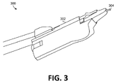
- FIGURE 3 illustrates an example of a single-tip test probe 300 in accordance with certain embodiments of the disclosed technology.
- the test probe 300 includes a test probe body 302 and a test probe tip 304, such as the test probe tips 100 and 200 illustrated by FIGURES 1 and 2 , respectively.
- a user may use the test probe 300 to create a compression resistance between the test probe tip 304 and a test point, such as a high-speed signal access point or other suitable point on a DUT, for example.
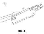
- FIGURE 4 illustrates an example of a differential probe 400 in accordance with certain embodiments of the disclosed technology.
- the differential probe 400 includes a probe body 402 and two test probe tips 404 and 406, such as the test probe tips 100 and 200 illustrated by FIGURES 1 and 2 , respectively.
- a user may use the differential probe 400 to create a compression resistance between either or both of the test probe tips 404 and 406 and one or two test points, such as a high-speed signal access point or other suitable point on a DUT, for example.
- FIGURE 5 is a graphical representation of an example of a frequency response plot 500 for a test probe tip in accordance with certain embodiments of the disclosed technology.
- the configuration of the resistor fabrication e.g., rod tube nature
- close proximity to the contact point of the DUT contact generates a highly flat response to signals on the DUT, yielding high signal reproduction fidelity while keeping DUT loading to a minimum. This is important for measuring signal busses that are sensitive to loading. If the tip/probe input structure loads (e.g., reduces or alters the signal eye) the signaling between transmitter-receiver is interrupted, the communication bus under test fails to work properly, which ruins the test.
- Probe tips in accordance with the disclosed technology advantageously limits this issue greatly.
- Examples provide a test probe tip, comprising a force deflecting assembly, a resistive/impedance element configured to be coupled with the force deflecting assembly, wherein the resistive/impedance element is a round rod resistor, and a tip component configured to be coupled with the resistive/impedance element.
- the force deflecting assembly includes a plunger component configured to be coupled with the resistive/impedance element, a barrel component configured to receive the plunger component, wherein the plunger component is configured to slide axially inside the barrel component, and a spring mechanism positioned within the barrel component and configured to act on the plunger component responsive to the plunger component sliding in an inward direction inside the barrel component.
- the resistive/impedance element is coupled with the plunger component by way of an electro-mechanical bond.
- the tip component is coupled with the resistive/impedance element by way of an electro-mechanical bond.
- the tip component includes at least one sharp point configured to establish an electrical connection with a test point on a device under test (DUT).
- DUT device under test
- the spring mechanism is configured to create a compression resistance between the probe tip and a test point on a device under test (DUT).
- DUT device under test
- the round rod resistor includes a resistive coating covering a tube.
- the metal connection of the round rod resistor includes a short overlapping tube on each end.
- test probe comprising a test probe body, and at least one test probe tip integrated with the test probe body, each test probe tip including a compliance member, a resistive/impedance element configured to be coupled with the compliance member, wherein the resistive/impedance element is a round rod resistor, and a tip component configured to be coupled with the resistive/impedance element.
- the compliance member includes a plunger component, a barrel component configured to receive the plunger component, wherein the plunger component is configured to slide axially inside the barrel component, and a spring mechanism positioned within the barrel component and configured to act on the plunger component responsive to the plunger component sliding in an inward direction inside the barrel component.
- the resistive/impedance element is coupled with the plunger component by way of an electro-mechanical bond.
- the tip component is coupled with the resistive/impedance element by way of an electro-mechanical bond.
- the tip component includes at least one sharp point configured to establish an electrical connection between the test probe and a test point on a device under test (DUT).
- DUT device under test
- the spring mechanism is configured to create a compression resistance between the test probe and a test point on a device under test (DUT).
- DUT device under test
- Some examples further comprise two test probe tips.
- the compliance member of each of the two test probe tips includes a plunger component, a barrel component configured to receive the plunger component, wherein the plunger component is configured to slide axially inside the barrel component, a spring mechanism positioned within the barrel component and configured to act on the plunger component responsive to the plunger component sliding in an inward direction inside the barrel component.
- the round rod resistor includes a resistive coating covering a tube.
- the metal connection of the round rod resistor includes a short overlapping tube on each end.
Landscapes
- Physics & Mathematics (AREA)
- General Physics & Mathematics (AREA)
- Measuring Leads Or Probes (AREA)
Abstract
Description
- This disclosure relates generally to test probes and, more particularly, to probe tips for test probes.
- Today's engineers are attempting to test devices that carry high-speed serial busses. Many of these devices can be identified as, but are not limited to, double data rate second generation (DDR2) synchronous dynamic random-access memory (SDRAM), double data rate fourth generation (DDR4) SDRAM, and peripheral component interconnect express (PCIe). The magnitude of voltage swings and pulse frequencies are very high and the complexity of the signaling requires precise electrical probing. These and other busses are becoming highly prevalent in various types of consumer hardware devices. There are many test points of interest in each of these products.
- The test points in these products vary greatly in both geometry and accessibility, usually requiring one or two points of contact. Typically, points of contact include micro traces, vias, component pads, and connector contacts that provide electrical contact with and, thus, access to high-speed signals. However, the test points are not always in the same plane and, if two probe contacts are required at once (e.g., as in the case of a differential probe), tip compliance is highly desirable to assist with positioning the probe for proper contact. Points of contact may reside on principal component analysis (PCA) hardware in virtually every angle of orientation, including from vertical to horizontal. In these types of scenarios, the test points are better accessed by probe tips with compliance.
- While there are semi-permanent forms of probe contact for these access points, including the soldering or conductive epoxying of wires to these points, such solutions present a number of disadvantages, including potential damage to the device under test (DUT) during connection, long set-up times, and a requirement for exceptional dexterity skills in order to solder wires to these test points. Also, semi-permanent contacts do not provide for quick debugging. Solder-in probe tips tend to wear out after only a few connections and, thus, create a need for replacements, which can be significantly expensive. Finally, there tends to be a high variability in the signal fidelity, particularly in upper signal frequencies, due to the quality and geometry of solder and/or epoxy connections.
- Accordingly, there remains a need for improved probe tips for use in connection with test probes.
- Embodiments of the disclosed technology generally pertain to probe tips suitable for use with test probes. A test probe tip may include a compliance member or force deflecting assembly that includes a barrel component that receives a plunger base coupled with a resistive/impedance element that is also coupled with a tip component. A spring mechanism may be trapped or otherwise positioned within the barrel component and the plunger base may be configured to slide axially inside the barrel component and be acted upon by the spring mechanism therein to advantageously create a compression resistance, e.g., with a test point on a DUT.
-
-
FIGURE 1 illustrates an exploded view of an example of a probe tip in accordance with certain embodiments of the disclosed technology. -
FIGURE 2 illustrates an assembled view of the probe tip illustrated byFIGURE 1 in accordance with certain embodiments of the disclosed technology. -
FIGURE 3 illustrates an example of a single-tip test probe in accordance with certain embodiments of the disclosed technology. -
FIGURE 4 illustrates an example of a differential probe in accordance with certain embodiments of the disclosed technology. -
FIGURE 5 is a graphical representation of an example of a frequency response plot for a test probe tip in accordance with certain embodiments of the disclosed technology. - Embodiments of the disclosed technology generally include probe tips suitable for use with a test probe and configured to provide a precise, height-compliant, quick, and light-pressure contact with a test point, e.g., on a device under test (DUT). Such a probe tip may be configured as a spring probe that includes a resistive or impedance element positioned nearly at the point of contact with the DUT. The resistive or impedance element may greatly improve the through response of the spring probe and also decrease the DUT loading significantly, thus enabling high-speed signal acquisition.
- Test probes and probe tips in accordance with the disclosed technology may advantageously create a better physical and electrical control of the contact area and also lend themselves well to fast debugging environments that typically cannot accommodate long contact setup times. Test probes and probe tips in accordance with the disclosed technology may advantageously provide superior visibility for connection placement and intuitive operation various classes of products, specifically hand-held or rapid placement probing.
-
FIGURE 1 illustrates an exploded view of an example of atest probe tip 100 in accordance with certain embodiments of the disclosed technology. In the example, thetest probe tip 100 includes a compliance member or force deflecting assembly and atip component 108 coupled therewith. - In the example, the compliance member or force deflecting assembly includes a
barrel component 102 configured to be integrated with a test probe. Theprobe tip 100 also includes a resistive/impedance element 106, e.g., a round rod resistor, and aplunger base component 104 configured to be coupled, e.g., by way of an electro-mechanical bond, with an end surface of the resistive/impedance element 106. - The resistive/
impedance element 106 may be have a tube-like form with resistance on the outside full circumference thereof. For example, the resistive/impedance element 106 may include a resistive coating that covers a tube and the metal connection may be a short overlapping tube on the ends. The tube-like structure of the resistor may enable high bandwidth, low bandwidth loading. Round surfaces of the resistive/impedance element 106 may advantageously maximize the cross-sectional strength of the resistive/impedance element 106. - In the example, the
tip component 108 is configured to be coupled, e.g., by way of an electro-mechanical bond, with an end surface of the resistive/impedance element 106 opposite the end surface that is coupled with theplunger base component 104. Thetip component 108 may have one or more sharp points, e.g., to establish or otherwise facilitate fine-grain electrical connectivity with one or more contact points on a DUT. - A spring mechanism may be trapped or otherwise positioned within the
barrel component 102, and theplunger base 104 may be configured to slide axially inside thebarrel component 102 and, consequently, be acted upon by the spring mechanism positioned inside thebarrel component 102 to advantageously create a compression resistance. -
FIGURE 2 illustrates an assembled view of an example of atest probe tip 200 having a compliance member or force deflecting assembly and a tip component coupled therewith in accordance with certain embodiments of the disclosed technology. In the example, abarrel component 202 receives aplunger base 204 that is coupled, e.g., by way of an electro-mechanical bond, with an end of a resistive/impedance element 206. The resistive/impedance element 206 may have a tube-like form with resistance on the outside full circumference thereof. In the example, atip component 208 is coupled, e.g., by way of an electro-mechanical bond, with an end of the resistive/impedance element 206 opposite the end thereof that is coupled with theplunger base 204. - As with the
test probe tip 100 illustrated byFIGURE 1 , a spring mechanism may be trapped or otherwise positioned within thebarrel component 202, and theplunger base 204 may be configured to slide axially inside thebarrel component 202 and be acted upon by the spring mechanism therein to advantageously create a compression resistance. -
FIGURE 3 illustrates an example of a single-tip test probe 300 in accordance with certain embodiments of the disclosed technology. In the example, thetest probe 300 includes atest probe body 302 and atest probe tip 304, such as thetest probe tips FIGURES 1 and2 , respectively. A user may use thetest probe 300 to create a compression resistance between thetest probe tip 304 and a test point, such as a high-speed signal access point or other suitable point on a DUT, for example. -
FIGURE 4 illustrates an example of adifferential probe 400 in accordance with certain embodiments of the disclosed technology. In the example, thedifferential probe 400 includes aprobe body 402 and twotest probe tips test probe tips FIGURES 1 and2 , respectively. A user may use thedifferential probe 400 to create a compression resistance between either or both of thetest probe tips -
FIGURE 5 is a graphical representation of an example of a frequency response plot 500 for a test probe tip in accordance with certain embodiments of the disclosed technology. The configuration of the resistor fabrication (e.g., rod tube nature) and close proximity to the contact point of the DUT contact generates a highly flat response to signals on the DUT, yielding high signal reproduction fidelity while keeping DUT loading to a minimum. This is important for measuring signal busses that are sensitive to loading. If the tip/probe input structure loads (e.g., reduces or alters the signal eye) the signaling between transmitter-receiver is interrupted, the communication bus under test fails to work properly, which ruins the test. Probe tips in accordance with the disclosed technology advantageously limits this issue greatly. - Examples provide a test probe tip, comprising a force deflecting assembly, a resistive/impedance element configured to be coupled with the force deflecting assembly, wherein the resistive/impedance element is a round rod resistor, and a tip component configured to be coupled with the resistive/impedance element.
- In some examples the force deflecting assembly includes a plunger component configured to be coupled with the resistive/impedance element, a barrel component configured to receive the plunger component, wherein the plunger component is configured to slide axially inside the barrel component, and a spring mechanism positioned within the barrel component and configured to act on the plunger component responsive to the plunger component sliding in an inward direction inside the barrel component.
- In some examples the resistive/impedance element is coupled with the plunger component by way of an electro-mechanical bond.
- In some examples the tip component is coupled with the resistive/impedance element by way of an electro-mechanical bond.
- In some examples the tip component includes at least one sharp point configured to establish an electrical connection with a test point on a device under test (DUT).
- In some examples the spring mechanism is configured to create a compression resistance between the probe tip and a test point on a device under test (DUT).
- In some examples the round rod resistor includes a resistive coating covering a tube.
- In some examples the metal connection of the round rod resistor includes a short overlapping tube on each end.
- Examples provide a test probe, comprising a test probe body, and at least one test probe tip integrated with the test probe body, each test probe tip including a compliance member, a resistive/impedance element configured to be coupled with the compliance member, wherein the resistive/impedance element is a round rod resistor, and a tip component configured to be coupled with the resistive/impedance element.
- In some examples the compliance member includes a plunger component, a barrel component configured to receive the plunger component, wherein the plunger component is configured to slide axially inside the barrel component, and a spring mechanism positioned within the barrel component and configured to act on the plunger component responsive to the plunger component sliding in an inward direction inside the barrel component.
- In some examples, the resistive/impedance element is coupled with the plunger component by way of an electro-mechanical bond.
- In some examples, the tip component is coupled with the resistive/impedance element by way of an electro-mechanical bond.
- In some examples, the tip component includes at least one sharp point configured to establish an electrical connection between the test probe and a test point on a device under test (DUT).
- In some examples, the spring mechanism is configured to create a compression resistance between the test probe and a test point on a device under test (DUT).
- Some examples further comprise two test probe tips.
- In some examples the compliance member of each of the two test probe tips includes a plunger component, a barrel component configured to receive the plunger component, wherein the plunger component is configured to slide axially inside the barrel component, a spring mechanism positioned within the barrel component and configured to act on the plunger component responsive to the plunger component sliding in an inward direction inside the barrel component.
- In some examples, the round rod resistor includes a resistive coating covering a tube.
- In some examples, the metal connection of the round rod resistor includes a short overlapping tube on each end.
- Having described and illustrated the principles of the invention with reference to illustrated embodiments, it will be recognized that the illustrated embodiments may be modified in arrangement and detail without departing from such principles, and may be combined in any desired manner. And although the foregoing discussion has focused on particular embodiments, other configurations are contemplated.
- In particular, even though expressions such as "according to an embodiment of the invention" or the like are used herein, these phrases are meant to generally reference embodiment possibilities, and are not intended to limit the invention to particular embodiment configurations. As used herein, these terms may reference the same or different embodiments that are combinable into other embodiments.
- Consequently, in view of the wide variety of permutations to the embodiments that are described herein, this detailed description and accompanying material is intended to be illustrative only, and should not be taken as limiting the scope of the invention. What is claimed as the invention, therefore, is all such modifications as may come within the scope of the following claims and equivalents thereto.
Claims (10)
- A test probe, comprising:a test probe body; andat least one test probe tip integrated with the test probe body, each test probe tip including:a compliance member;a resistive/impedance element configured to be coupled with the compliance member, wherein the resistive/impedance element is a round rod resistor; anda tip component configured to be coupled with the resistive/impedance element.
- The test probe of claim 1, wherein the compliance member includes:a plunger component;a barrel component configured to receive the plunger component,wherein the plunger component is configured to slide axially inside the barrel component; anda spring mechanism positioned within the barrel component and configured to act on the plunger component responsive to the plunger component sliding in an inward direction inside the barrel component.
- The test probe of claim 2, wherein the resistive/impedance element is coupled with the plunger component by way of an electro-mechanical bond.
- The test probe of any of claims 1 to 3, wherein the tip component is coupled with the resistive/impedance element by way of an electro-mechanical bond.
- The test probe of any of claims 1 to 4, wherein the tip component includes at least one sharp point configured to establish an electrical connection between the test probe and a test point on a device under test, DUT.
- The test probe of claim 2, wherein the spring mechanism is configured to create a compression resistance between the test probe and a test point on a device under test, DUT.
- The test probe of any of claims 1 to 6, further comprising two test probe tips.
- The test probe of claim 7, wherein the compliance member of each of the two test probe tips includes:a plunger component;a barrel component configured to receive the plunger component,wherein the plunger component is configured to slide axially inside the barrel component;a spring mechanism positioned within the barrel component and configured to act on the plunger component responsive to the plunger component sliding in an inward direction inside the barrel component.
- The test probe of any of claims 1 to 8, wherein the round rod resistor includes a resistive coating covering a tube.
- The test probe tip of claim 9, wherein the metal connection of the round rod resistor includes a short overlapping tube on each end.
Applications Claiming Priority (1)
| Application Number | Priority Date | Filing Date | Title |
|---|---|---|---|
| US14/587,703 US9810715B2 (en) | 2014-12-31 | 2014-12-31 | High impedance compliant probe tip |
Publications (2)
| Publication Number | Publication Date |
|---|---|
| EP3056912A1 true EP3056912A1 (en) | 2016-08-17 |
| EP3056912B1 EP3056912B1 (en) | 2021-04-07 |
Family
ID=55068911
Family Applications (1)
| Application Number | Title | Priority Date | Filing Date |
|---|---|---|---|
| EP15203192.8A Active EP3056912B1 (en) | 2014-12-31 | 2015-12-30 | High frequency probe tip |
Country Status (4)
| Country | Link |
|---|---|
| US (1) | US9810715B2 (en) |
| EP (1) | EP3056912B1 (en) |
| JP (1) | JP7231977B2 (en) |
| CN (1) | CN105938152A (en) |
Cited By (1)
| Publication number | Priority date | Publication date | Assignee | Title |
|---|---|---|---|---|
| US10886588B2 (en) | 2018-09-26 | 2021-01-05 | Keysight Technologies, Inc. | High dynamic range probe using pole-zero cancellation |
Families Citing this family (14)
| Publication number | Priority date | Publication date | Assignee | Title |
|---|---|---|---|---|
| HUP1700051A2 (en) * | 2017-02-02 | 2018-08-28 | Equip Test Kft | Contact device and headunit, and method of contact device and headunit production |
| US10753961B2 (en) * | 2017-05-10 | 2020-08-25 | Tektronix, Inc. | Shielded probe tip interface |
| US10845384B2 (en) * | 2017-11-07 | 2020-11-24 | Tektronix. Inc. | Surface-mountable apparatus for coupling a test and measurement instrument to a device under test |
| CN109752574A (en) * | 2017-11-07 | 2019-05-14 | 特克特朗尼克公司 | Probe end and probe assembly |
| TWD197822S (en) * | 2018-02-02 | 2019-06-01 | Nihon Micronics Kk | Part of electric contact |
| JP1622970S (en) * | 2018-02-02 | 2019-01-28 | ||
| JP1622968S (en) * | 2018-02-02 | 2019-01-28 | ||
| JP1622969S (en) * | 2018-02-02 | 2019-01-28 | ||
| JP1626668S (en) * | 2018-02-02 | 2019-03-18 | ||
| JP1623279S (en) * | 2018-02-02 | 2019-01-28 | ||
| JP1626667S (en) * | 2018-02-02 | 2019-03-18 | ||
| JP1623280S (en) * | 2018-02-02 | 2019-01-28 | ||
| US11079408B2 (en) * | 2018-05-18 | 2021-08-03 | Tektronix, Inc. | Resistive test-probe tips |
| USD904212S1 (en) * | 2019-04-15 | 2020-12-08 | Ingun Prüfmittelbau Gmbh | Self-cleaning head shape |
Citations (7)
| Publication number | Priority date | Publication date | Assignee | Title |
|---|---|---|---|---|
| US2849681A (en) * | 1955-12-21 | 1958-08-26 | Prec Apparatus Co Inc | Electrical probe |
| DE8417746U1 (en) * | 1984-06-12 | 1986-01-09 | Feinmetall Gmbh, 7033 Herrenberg | Contact element |
| DE3533227A1 (en) * | 1984-09-27 | 1986-04-03 | Feinmetall Gmbh, 7033 Herrenberg | Spring contact pin |
| US20030222665A1 (en) * | 2002-04-18 | 2003-12-04 | Dascher David J. | Voltage probe systems having improved bandwidth capability |
| US20050079772A1 (en) * | 2003-10-14 | 2005-04-14 | The Ludlow Company, Lp | Cable terminal with air-enhanced contact pins |
| US7116121B1 (en) * | 2005-10-27 | 2006-10-03 | Agilent Technologies, Inc. | Probe assembly with controlled impedance spring pin or resistor tip spring pin contacts |
| DE102009008156A1 (en) * | 2009-02-09 | 2010-08-19 | Ingun Prüfmittelbau Gmbh | Cylindrical electrical high frequency test probe for use in testing field and/or measuring system, has inner and outer piston sections electrically connected with separate ohmic resistance body axially arranged between piston sections |
Family Cites Families (37)
| Publication number | Priority date | Publication date | Assignee | Title |
|---|---|---|---|---|
| US3136973A (en) * | 1961-09-18 | 1964-06-09 | Cons Electronics Ind | Sealed resistor |
| US3174123A (en) * | 1963-01-28 | 1965-03-16 | Blossy D Frederico | High power hybrid-l coaxial attenuator with t-fitting for inner conductors |
| US3578428A (en) * | 1968-11-04 | 1971-05-11 | Jobling & Co James A | Methods of producing ceramic material in rod or tube form |
| US3859568A (en) * | 1974-01-16 | 1975-01-07 | Gen Electric | Overvoltage surge arrester with improved voltage grading circuit |
| US4884034A (en) * | 1989-01-03 | 1989-11-28 | Hermilo Guzman | Ground fault detector and locator |
| US5045780A (en) * | 1989-12-04 | 1991-09-03 | Everett/Charles Contact Products, Inc. | Electrical test probe contact tip |
| JP2559875B2 (en) * | 1990-03-16 | 1996-12-04 | 日本碍子株式会社 | Resistor element |
| US5136237A (en) | 1991-01-29 | 1992-08-04 | Tektronix, Inc. | Double insulated floating high voltage test probe |
| US5106312A (en) * | 1991-06-27 | 1992-04-21 | Yeh Ming H | Coaxial cable output terminal safety plug device |
| JPH05175002A (en) * | 1991-12-20 | 1993-07-13 | Rohm Co Ltd | Cylindrical electronic component |
| JPH0613202A (en) * | 1992-06-26 | 1994-01-21 | Matsushita Electric Ind Co Ltd | Resistor |
| JP3112765B2 (en) * | 1993-03-15 | 2000-11-27 | 日本碍子株式会社 | Thermal flow meter |
| JPH0886808A (en) * | 1994-07-20 | 1996-04-02 | Sony Tektronix Corp | High voltage probe |
| JP2000260601A (en) * | 1999-03-08 | 2000-09-22 | Matsushita Electric Ind Co Ltd | Resistor and manufacturing method thereof |
| US6222378B1 (en) | 1999-05-28 | 2001-04-24 | Tektronix, Inc. | Probe adapter for a ball-grid-array package |
| WO2002010675A1 (en) | 2000-07-31 | 2002-02-07 | Lecroy Corporation | Electrical test probe flexible spring tip |
| USD444401S1 (en) | 2000-07-31 | 2001-07-03 | Lecroy Corporation | Electrical test probe wedge tip |
| US6605934B1 (en) | 2000-07-31 | 2003-08-12 | Lecroy Corporation | Cartridge system for a probing head for an electrical test probe |
| US6538424B1 (en) | 2000-07-31 | 2003-03-25 | Le Croy Corporation | Notched electrical test probe tip |
| USD444720S1 (en) | 2000-07-31 | 2001-07-10 | Lecroy Corporation | Notched electrical test probe tip |
| USD444721S1 (en) | 2000-07-31 | 2001-07-10 | Lecroy Corporation | Electrical test probe probing head |
| US6518780B1 (en) | 2000-07-31 | 2003-02-11 | Lecroy Corporation | Electrical test probe wedge tip |
| US6462529B1 (en) | 2000-07-31 | 2002-10-08 | Lecroy Corporation | Legs for trimming a tripod with an electrical test probe tip |
| US6433527B1 (en) * | 2001-06-01 | 2002-08-13 | Maxim Integrated Products, Inc. | Phase failure detector for multi-phase switching regulators |
| US6956362B1 (en) | 2001-12-14 | 2005-10-18 | Lecroy Corporation | Modular active test probe and removable tip module therefor |
| US6822463B1 (en) | 2001-12-21 | 2004-11-23 | Lecroy Corporation | Active differential test probe with a transmission line input structure |
| US7173439B1 (en) | 2003-02-14 | 2007-02-06 | Lecroy Corporation | Guide for tip to transmission path contact |
| US7317312B1 (en) | 2003-02-14 | 2008-01-08 | Lecroy Corporation | Guide for tip to transmission path contact |
| US7321234B2 (en) | 2003-12-18 | 2008-01-22 | Lecroy Corporation | Resistive test probe tips and applications therefor |
| US7262614B1 (en) | 2005-02-10 | 2007-08-28 | Lecroy Corporation | Planar on edge probing tip with flex |
| US7202678B2 (en) | 2003-12-18 | 2007-04-10 | Lecroy Corporation | Resistive probe tips |
| WO2005060718A2 (en) | 2003-12-18 | 2005-07-07 | Lecroy Corporation | Cap at resistors of electrical test probe |
| US7221179B1 (en) | 2003-12-18 | 2007-05-22 | Lecroy Corporation | Bendable conductive connector |
| US7894174B2 (en) * | 2004-08-23 | 2011-02-22 | Monolithic Power Systems, Inc. | Method and apparatus for fault detection scheme for cold cathode fluorescent lamp (CCFL) integrated circuits |
| US7242202B2 (en) * | 2005-05-31 | 2007-07-10 | Agilent Technologies, Inc. | Signal probe and probe assembly |
| US8134377B1 (en) | 2005-08-31 | 2012-03-13 | Lecroy Corporation | Adherable holder and locater tool |
| US7671613B1 (en) | 2006-01-06 | 2010-03-02 | Lecroy Corporation | Probing blade conductive connector for use with an electrical test probe |
-
2014
- 2014-12-31 US US14/587,703 patent/US9810715B2/en active Active
-
2015
- 2015-12-29 JP JP2015257610A patent/JP7231977B2/en active Active
- 2015-12-30 EP EP15203192.8A patent/EP3056912B1/en active Active
- 2015-12-31 CN CN201511036011.6A patent/CN105938152A/en active Pending
Patent Citations (7)
| Publication number | Priority date | Publication date | Assignee | Title |
|---|---|---|---|---|
| US2849681A (en) * | 1955-12-21 | 1958-08-26 | Prec Apparatus Co Inc | Electrical probe |
| DE8417746U1 (en) * | 1984-06-12 | 1986-01-09 | Feinmetall Gmbh, 7033 Herrenberg | Contact element |
| DE3533227A1 (en) * | 1984-09-27 | 1986-04-03 | Feinmetall Gmbh, 7033 Herrenberg | Spring contact pin |
| US20030222665A1 (en) * | 2002-04-18 | 2003-12-04 | Dascher David J. | Voltage probe systems having improved bandwidth capability |
| US20050079772A1 (en) * | 2003-10-14 | 2005-04-14 | The Ludlow Company, Lp | Cable terminal with air-enhanced contact pins |
| US7116121B1 (en) * | 2005-10-27 | 2006-10-03 | Agilent Technologies, Inc. | Probe assembly with controlled impedance spring pin or resistor tip spring pin contacts |
| DE102009008156A1 (en) * | 2009-02-09 | 2010-08-19 | Ingun Prüfmittelbau Gmbh | Cylindrical electrical high frequency test probe for use in testing field and/or measuring system, has inner and outer piston sections electrically connected with separate ohmic resistance body axially arranged between piston sections |
Non-Patent Citations (1)
| Title |
|---|
| JIS-C: "Carbon Film MELF Resistors", 1 June 2011 (2011-06-01), pages 1 - 2, XP055277810, Retrieved from the Internet <URL:http://www.cinetech.com.tw/upload/2011/06/20110617152049.pdf> [retrieved on 20160603] * |
Cited By (1)
| Publication number | Priority date | Publication date | Assignee | Title |
|---|---|---|---|---|
| US10886588B2 (en) | 2018-09-26 | 2021-01-05 | Keysight Technologies, Inc. | High dynamic range probe using pole-zero cancellation |
Also Published As
| Publication number | Publication date |
|---|---|
| JP2016126018A (en) | 2016-07-11 |
| US9810715B2 (en) | 2017-11-07 |
| CN105938152A (en) | 2016-09-14 |
| EP3056912B1 (en) | 2021-04-07 |
| US20160187382A1 (en) | 2016-06-30 |
| JP7231977B2 (en) | 2023-03-02 |
Similar Documents
| Publication | Publication Date | Title |
|---|---|---|
| US9810715B2 (en) | High impedance compliant probe tip | |
| US10241133B2 (en) | Probe tip and probe assembly | |
| US10119992B2 (en) | High impedance compliant probe tip | |
| US20180080955A1 (en) | Bolt type probe | |
| CN106716145A (en) | Contact probes for test fixtures | |
| CN110133328A (en) | Detector | |
| JP2016520835A (en) | Test probe, test probe assembly and test platform | |
| KR101956650B1 (en) | Ground spring with strain relief | |
| TWI582434B (en) | Probe device | |
| CN110501537B (en) | Resistive Test Probe Tips | |
| US20140266277A1 (en) | Semiconductor testing probe needle | |
| US10845384B2 (en) | Surface-mountable apparatus for coupling a test and measurement instrument to a device under test | |
| CN109164346B (en) | Automobile connector detection device | |
| JP2019086519A (en) | Test probe and test probe tip | |
| CN110416791B (en) | Pogo pin connector | |
| CN208902823U (en) | A kind of automobile connector detection device | |
| CN111721977B (en) | Surface mountable device that couples test and measurement instruments to the device under test | |
| JP3183676U (en) | Probe pin for semiconductor inspection | |
| CN223284238U (en) | A high-impedance contact electrostatic tester | |
| CN112129975A (en) | Electrical connection assembly | |
| KR101509418B1 (en) | A probe card with non-resistibility | |
| TWI617811B (en) | Probe card | |
| CN104714059A (en) | Test joint | |
| TWM453149U (en) | Concentric testing pins | |
| TWM478823U (en) | signal adaptor structure of probe detector |
Legal Events
| Date | Code | Title | Description |
|---|---|---|---|
| PUAI | Public reference made under article 153(3) epc to a published international application that has entered the european phase |
Free format text: ORIGINAL CODE: 0009012 |
|
| AK | Designated contracting states |
Kind code of ref document: A1 Designated state(s): AL AT BE BG CH CY CZ DE DK EE ES FI FR GB GR HR HU IE IS IT LI LT LU LV MC MK MT NL NO PL PT RO RS SE SI SK SM TR |
|
| AX | Request for extension of the european patent |
Extension state: BA ME |
|
| STAA | Information on the status of an ep patent application or granted ep patent |
Free format text: STATUS: REQUEST FOR EXAMINATION WAS MADE |
|
| 17P | Request for examination filed |
Effective date: 20170217 |
|
| RBV | Designated contracting states (corrected) |
Designated state(s): AL AT BE BG CH CY CZ DE DK EE ES FI FR GB GR HR HU IE IS IT LI LT LU LV MC MK MT NL NO PL PT RO RS SE SI SK SM TR |
|
| RIN1 | Information on inventor provided before grant (corrected) |
Inventor name: ENNS, CHRISTINA Inventor name: POLLOCK, IRA Inventor name: CAMPBELL, JULIE Inventor name: HAGERUP, WILLIAM |
|
| STAA | Information on the status of an ep patent application or granted ep patent |
Free format text: STATUS: EXAMINATION IS IN PROGRESS |
|
| 17Q | First examination report despatched |
Effective date: 20180409 |
|
| REG | Reference to a national code |
Ref country code: DE Ref legal event code: R079 Ref document number: 602015067707 Country of ref document: DE Free format text: PREVIOUS MAIN CLASS: G01R0001067000 Ipc: H01R0101000000 |
|
| GRAP | Despatch of communication of intention to grant a patent |
Free format text: ORIGINAL CODE: EPIDOSNIGR1 |
|
| STAA | Information on the status of an ep patent application or granted ep patent |
Free format text: STATUS: GRANT OF PATENT IS INTENDED |
|
| RIC1 | Information provided on ipc code assigned before grant |
Ipc: H01R 13/24 20060101ALI20200925BHEP Ipc: G01R 1/067 20060101ALI20200925BHEP Ipc: G01R 1/073 20060101ALI20200925BHEP Ipc: H01R 101/00 20060101AFI20200925BHEP |
|
| INTG | Intention to grant announced |
Effective date: 20201016 |
|
| GRAS | Grant fee paid |
Free format text: ORIGINAL CODE: EPIDOSNIGR3 |
|
| GRAA | (expected) grant |
Free format text: ORIGINAL CODE: 0009210 |
|
| STAA | Information on the status of an ep patent application or granted ep patent |
Free format text: STATUS: THE PATENT HAS BEEN GRANTED |
|
| AK | Designated contracting states |
Kind code of ref document: B1 Designated state(s): AL AT BE BG CH CY CZ DE DK EE ES FI FR GB GR HR HU IE IS IT LI LT LU LV MC MK MT NL NO PL PT RO RS SE SI SK SM TR |
|
| REG | Reference to a national code |
Ref country code: GB Ref legal event code: FG4D |
|
| REG | Reference to a national code |
Ref country code: AT Ref legal event code: REF Ref document number: 1380905 Country of ref document: AT Kind code of ref document: T Effective date: 20210415 Ref country code: CH Ref legal event code: EP |
|
| REG | Reference to a national code |
Ref country code: DE Ref legal event code: R096 Ref document number: 602015067707 Country of ref document: DE |
|
| REG | Reference to a national code |
Ref country code: IE Ref legal event code: FG4D |
|
| REG | Reference to a national code |
Ref country code: LT Ref legal event code: MG9D |
|
| REG | Reference to a national code |
Ref country code: NL Ref legal event code: MP Effective date: 20210407 Ref country code: AT Ref legal event code: MK05 Ref document number: 1380905 Country of ref document: AT Kind code of ref document: T Effective date: 20210407 |
|
| PG25 | Lapsed in a contracting state [announced via postgrant information from national office to epo] |
Ref country code: FI Free format text: LAPSE BECAUSE OF FAILURE TO SUBMIT A TRANSLATION OF THE DESCRIPTION OR TO PAY THE FEE WITHIN THE PRESCRIBED TIME-LIMIT Effective date: 20210407 Ref country code: NL Free format text: LAPSE BECAUSE OF FAILURE TO SUBMIT A TRANSLATION OF THE DESCRIPTION OR TO PAY THE FEE WITHIN THE PRESCRIBED TIME-LIMIT Effective date: 20210407 Ref country code: LT Free format text: LAPSE BECAUSE OF FAILURE TO SUBMIT A TRANSLATION OF THE DESCRIPTION OR TO PAY THE FEE WITHIN THE PRESCRIBED TIME-LIMIT Effective date: 20210407 Ref country code: HR Free format text: LAPSE BECAUSE OF FAILURE TO SUBMIT A TRANSLATION OF THE DESCRIPTION OR TO PAY THE FEE WITHIN THE PRESCRIBED TIME-LIMIT Effective date: 20210407 Ref country code: AT Free format text: LAPSE BECAUSE OF FAILURE TO SUBMIT A TRANSLATION OF THE DESCRIPTION OR TO PAY THE FEE WITHIN THE PRESCRIBED TIME-LIMIT Effective date: 20210407 Ref country code: BG Free format text: LAPSE BECAUSE OF FAILURE TO SUBMIT A TRANSLATION OF THE DESCRIPTION OR TO PAY THE FEE WITHIN THE PRESCRIBED TIME-LIMIT Effective date: 20210707 |
|
| PG25 | Lapsed in a contracting state [announced via postgrant information from national office to epo] |
Ref country code: LV Free format text: LAPSE BECAUSE OF FAILURE TO SUBMIT A TRANSLATION OF THE DESCRIPTION OR TO PAY THE FEE WITHIN THE PRESCRIBED TIME-LIMIT Effective date: 20210407 Ref country code: GR Free format text: LAPSE BECAUSE OF FAILURE TO SUBMIT A TRANSLATION OF THE DESCRIPTION OR TO PAY THE FEE WITHIN THE PRESCRIBED TIME-LIMIT Effective date: 20210708 Ref country code: IS Free format text: LAPSE BECAUSE OF FAILURE TO SUBMIT A TRANSLATION OF THE DESCRIPTION OR TO PAY THE FEE WITHIN THE PRESCRIBED TIME-LIMIT Effective date: 20210807 Ref country code: ES Free format text: LAPSE BECAUSE OF FAILURE TO SUBMIT A TRANSLATION OF THE DESCRIPTION OR TO PAY THE FEE WITHIN THE PRESCRIBED TIME-LIMIT Effective date: 20210407 Ref country code: PL Free format text: LAPSE BECAUSE OF FAILURE TO SUBMIT A TRANSLATION OF THE DESCRIPTION OR TO PAY THE FEE WITHIN THE PRESCRIBED TIME-LIMIT Effective date: 20210407 Ref country code: NO Free format text: LAPSE BECAUSE OF FAILURE TO SUBMIT A TRANSLATION OF THE DESCRIPTION OR TO PAY THE FEE WITHIN THE PRESCRIBED TIME-LIMIT Effective date: 20210707 Ref country code: PT Free format text: LAPSE BECAUSE OF FAILURE TO SUBMIT A TRANSLATION OF THE DESCRIPTION OR TO PAY THE FEE WITHIN THE PRESCRIBED TIME-LIMIT Effective date: 20210809 Ref country code: SE Free format text: LAPSE BECAUSE OF FAILURE TO SUBMIT A TRANSLATION OF THE DESCRIPTION OR TO PAY THE FEE WITHIN THE PRESCRIBED TIME-LIMIT Effective date: 20210407 Ref country code: RS Free format text: LAPSE BECAUSE OF FAILURE TO SUBMIT A TRANSLATION OF THE DESCRIPTION OR TO PAY THE FEE WITHIN THE PRESCRIBED TIME-LIMIT Effective date: 20210407 |
|
| REG | Reference to a national code |
Ref country code: DE Ref legal event code: R097 Ref document number: 602015067707 Country of ref document: DE |
|
| PG25 | Lapsed in a contracting state [announced via postgrant information from national office to epo] |
Ref country code: SK Free format text: LAPSE BECAUSE OF FAILURE TO SUBMIT A TRANSLATION OF THE DESCRIPTION OR TO PAY THE FEE WITHIN THE PRESCRIBED TIME-LIMIT Effective date: 20210407 Ref country code: SM Free format text: LAPSE BECAUSE OF FAILURE TO SUBMIT A TRANSLATION OF THE DESCRIPTION OR TO PAY THE FEE WITHIN THE PRESCRIBED TIME-LIMIT Effective date: 20210407 Ref country code: DK Free format text: LAPSE BECAUSE OF FAILURE TO SUBMIT A TRANSLATION OF THE DESCRIPTION OR TO PAY THE FEE WITHIN THE PRESCRIBED TIME-LIMIT Effective date: 20210407 Ref country code: EE Free format text: LAPSE BECAUSE OF FAILURE TO SUBMIT A TRANSLATION OF THE DESCRIPTION OR TO PAY THE FEE WITHIN THE PRESCRIBED TIME-LIMIT Effective date: 20210407 Ref country code: CZ Free format text: LAPSE BECAUSE OF FAILURE TO SUBMIT A TRANSLATION OF THE DESCRIPTION OR TO PAY THE FEE WITHIN THE PRESCRIBED TIME-LIMIT Effective date: 20210407 Ref country code: RO Free format text: LAPSE BECAUSE OF FAILURE TO SUBMIT A TRANSLATION OF THE DESCRIPTION OR TO PAY THE FEE WITHIN THE PRESCRIBED TIME-LIMIT Effective date: 20210407 |
|
| PLBE | No opposition filed within time limit |
Free format text: ORIGINAL CODE: 0009261 |
|
| STAA | Information on the status of an ep patent application or granted ep patent |
Free format text: STATUS: NO OPPOSITION FILED WITHIN TIME LIMIT |
|
| 26N | No opposition filed |
Effective date: 20220110 |
|
| PG25 | Lapsed in a contracting state [announced via postgrant information from national office to epo] |
Ref country code: IS Free format text: LAPSE BECAUSE OF FAILURE TO SUBMIT A TRANSLATION OF THE DESCRIPTION OR TO PAY THE FEE WITHIN THE PRESCRIBED TIME-LIMIT Effective date: 20210807 Ref country code: AL Free format text: LAPSE BECAUSE OF FAILURE TO SUBMIT A TRANSLATION OF THE DESCRIPTION OR TO PAY THE FEE WITHIN THE PRESCRIBED TIME-LIMIT Effective date: 20210407 |
|
| PG25 | Lapsed in a contracting state [announced via postgrant information from national office to epo] |
Ref country code: MC Free format text: LAPSE BECAUSE OF FAILURE TO SUBMIT A TRANSLATION OF THE DESCRIPTION OR TO PAY THE FEE WITHIN THE PRESCRIBED TIME-LIMIT Effective date: 20210407 Ref country code: IT Free format text: LAPSE BECAUSE OF FAILURE TO SUBMIT A TRANSLATION OF THE DESCRIPTION OR TO PAY THE FEE WITHIN THE PRESCRIBED TIME-LIMIT Effective date: 20210407 |
|
| REG | Reference to a national code |
Ref country code: CH Ref legal event code: PL |
|
| GBPC | Gb: european patent ceased through non-payment of renewal fee |
Effective date: 20211230 |
|
| REG | Reference to a national code |
Ref country code: BE Ref legal event code: MM Effective date: 20211231 |
|
| PG25 | Lapsed in a contracting state [announced via postgrant information from national office to epo] |
Ref country code: LU Free format text: LAPSE BECAUSE OF NON-PAYMENT OF DUE FEES Effective date: 20211230 Ref country code: IE Free format text: LAPSE BECAUSE OF NON-PAYMENT OF DUE FEES Effective date: 20211230 Ref country code: GB Free format text: LAPSE BECAUSE OF NON-PAYMENT OF DUE FEES Effective date: 20211230 |
|
| PG25 | Lapsed in a contracting state [announced via postgrant information from national office to epo] |
Ref country code: FR Free format text: LAPSE BECAUSE OF NON-PAYMENT OF DUE FEES Effective date: 20211231 Ref country code: BE Free format text: LAPSE BECAUSE OF NON-PAYMENT OF DUE FEES Effective date: 20211231 |
|
| PG25 | Lapsed in a contracting state [announced via postgrant information from national office to epo] |
Ref country code: LI Free format text: LAPSE BECAUSE OF NON-PAYMENT OF DUE FEES Effective date: 20211231 Ref country code: CH Free format text: LAPSE BECAUSE OF NON-PAYMENT OF DUE FEES Effective date: 20211231 |
|
| PG25 | Lapsed in a contracting state [announced via postgrant information from national office to epo] |
Ref country code: HU Free format text: LAPSE BECAUSE OF FAILURE TO SUBMIT A TRANSLATION OF THE DESCRIPTION OR TO PAY THE FEE WITHIN THE PRESCRIBED TIME-LIMIT; INVALID AB INITIO Effective date: 20151230 |
|
| PG25 | Lapsed in a contracting state [announced via postgrant information from national office to epo] |
Ref country code: CY Free format text: LAPSE BECAUSE OF FAILURE TO SUBMIT A TRANSLATION OF THE DESCRIPTION OR TO PAY THE FEE WITHIN THE PRESCRIBED TIME-LIMIT Effective date: 20210407 |
|
| P01 | Opt-out of the competence of the unified patent court (upc) registered |
Effective date: 20230530 |
|
| PG25 | Lapsed in a contracting state [announced via postgrant information from national office to epo] |
Ref country code: MK Free format text: LAPSE BECAUSE OF FAILURE TO SUBMIT A TRANSLATION OF THE DESCRIPTION OR TO PAY THE FEE WITHIN THE PRESCRIBED TIME-LIMIT Effective date: 20210407 |
|
| PG25 | Lapsed in a contracting state [announced via postgrant information from national office to epo] |
Ref country code: MT Free format text: LAPSE BECAUSE OF FAILURE TO SUBMIT A TRANSLATION OF THE DESCRIPTION OR TO PAY THE FEE WITHIN THE PRESCRIBED TIME-LIMIT Effective date: 20210407 |
|
| PG25 | Lapsed in a contracting state [announced via postgrant information from national office to epo] |
Ref country code: TR Free format text: LAPSE BECAUSE OF FAILURE TO SUBMIT A TRANSLATION OF THE DESCRIPTION OR TO PAY THE FEE WITHIN THE PRESCRIBED TIME-LIMIT Effective date: 20210407 |
|
| PGFP | Annual fee paid to national office [announced via postgrant information from national office to epo] |
Ref country code: DE Payment date: 20251229 Year of fee payment: 11 |