EP3054748A1 - Microplasma spray element, laminated microplasma spray module and method for manufacturing microplasma spray element - Google Patents
Microplasma spray element, laminated microplasma spray module and method for manufacturing microplasma spray element Download PDFInfo
- Publication number
- EP3054748A1 EP3054748A1 EP14850871.6A EP14850871A EP3054748A1 EP 3054748 A1 EP3054748 A1 EP 3054748A1 EP 14850871 A EP14850871 A EP 14850871A EP 3054748 A1 EP3054748 A1 EP 3054748A1
- Authority
- EP
- European Patent Office
- Prior art keywords
- plasma generation
- insulating layer
- generation electrode
- substrate
- layer
- Prior art date
- Legal status (The legal status is an assumption and is not a legal conclusion. Google has not performed a legal analysis and makes no representation as to the accuracy of the status listed.)
- Granted
Links
Images




Classifications
-
- H—ELECTRICITY
- H05—ELECTRIC TECHNIQUES NOT OTHERWISE PROVIDED FOR
- H05H—PLASMA TECHNIQUE; PRODUCTION OF ACCELERATED ELECTRICALLY-CHARGED PARTICLES OR OF NEUTRONS; PRODUCTION OR ACCELERATION OF NEUTRAL MOLECULAR OR ATOMIC BEAMS
- H05H1/00—Generating plasma; Handling plasma
- H05H1/24—Generating plasma
- H05H1/26—Plasma torches
- H05H1/32—Plasma torches using an arc
- H05H1/34—Details, e.g. electrodes, nozzles
-
- H—ELECTRICITY
- H05—ELECTRIC TECHNIQUES NOT OTHERWISE PROVIDED FOR
- H05H—PLASMA TECHNIQUE; PRODUCTION OF ACCELERATED ELECTRICALLY-CHARGED PARTICLES OR OF NEUTRONS; PRODUCTION OR ACCELERATION OF NEUTRAL MOLECULAR OR ATOMIC BEAMS
- H05H1/00—Generating plasma; Handling plasma
- H05H1/24—Generating plasma
- H05H1/2406—Generating plasma using dielectric barrier discharges, i.e. with a dielectric interposed between the electrodes
-
- H—ELECTRICITY
- H01—ELECTRIC ELEMENTS
- H01J—ELECTRIC DISCHARGE TUBES OR DISCHARGE LAMPS
- H01J37/00—Discharge tubes with provision for introducing objects or material to be exposed to the discharge, e.g. for the purpose of examination or processing thereof
- H01J37/32—Gas-filled discharge tubes
- H01J37/32431—Constructional details of the reactor
- H01J37/32458—Vessel
- H01J37/32467—Material
-
- H—ELECTRICITY
- H01—ELECTRIC ELEMENTS
- H01J—ELECTRIC DISCHARGE TUBES OR DISCHARGE LAMPS
- H01J37/00—Discharge tubes with provision for introducing objects or material to be exposed to the discharge, e.g. for the purpose of examination or processing thereof
- H01J37/32—Gas-filled discharge tubes
- H01J37/32431—Constructional details of the reactor
- H01J37/32532—Electrodes
-
- H—ELECTRICITY
- H05—ELECTRIC TECHNIQUES NOT OTHERWISE PROVIDED FOR
- H05H—PLASMA TECHNIQUE; PRODUCTION OF ACCELERATED ELECTRICALLY-CHARGED PARTICLES OR OF NEUTRONS; PRODUCTION OR ACCELERATION OF NEUTRAL MOLECULAR OR ATOMIC BEAMS
- H05H1/00—Generating plasma; Handling plasma
- H05H1/24—Generating plasma
- H05H1/2406—Generating plasma using dielectric barrier discharges, i.e. with a dielectric interposed between the electrodes
- H05H1/2437—Multilayer systems
-
- H—ELECTRICITY
- H05—ELECTRIC TECHNIQUES NOT OTHERWISE PROVIDED FOR
- H05H—PLASMA TECHNIQUE; PRODUCTION OF ACCELERATED ELECTRICALLY-CHARGED PARTICLES OR OF NEUTRONS; PRODUCTION OR ACCELERATION OF NEUTRAL MOLECULAR OR ATOMIC BEAMS
- H05H2245/00—Applications of plasma devices
- H05H2245/40—Surface treatments
Definitions
- the present invention relates to a plasma jet device, and more particularly, to a microplasma jet device capable of processing a large area, a laminated microplasma jet module, and a method of manufacturing the microplasma jet device.
- Plasma has been applied in various fields such as the semiconductor industry, the display industry, and for surface modification of materials. Recently, attempts to apply plasma to a bio-medical technology or surface processing of a material such as plastic or fiber have been made. However, in these applications, since an object material that should be treated by the plasma is sensitive to heat, a glow discharge, which is low-temperature plasma, should be used. Because glow discharge is very unstable at normal pressure, a glow-to-arc transition (GAT) in which the glow discharge is transitioned to an arc discharge, which is high-temperature plasma, is likely to occur.
- GAT glow-to-arc transition
- the GAT occurs by heat generated while the plasma is generated, and research on microplasma generated by reducing the capacity of the plasma has been progressing as a method of preventing the GAT.
- devices for generating microplasma cause discharge using needles or tubes which are mechanically processed.
- needles or tubes which are mechanically processed.
- an area that can be processed at one time is limited.
- the present invention is directed to providing a microplasma jet device capable of processing a larger area, a laminated microplasma jet module, and a method of manufacturing the microplasma jet device.
- One aspect of the present invention provides a microplasma jet device including: a channel layer having a plurality of microfluidic channels arranged in parallel so as to enable a gas for generating plasma to pass therethrough; a first insulating layer bonded to one surface of the channel layer and in which a first plasma generation electrode is formed; and a second insulating layer bonded to another surface of the channel layer and in which a second plasma generation electrode is formed.
- the microplasma jet device may further include a first substrate to which the first insulating layer is fixed and a second substrate to which the second insulating layer is fixed.
- the channel layer may be made of a polymer-based material.
- the polymer-based material may include polydimethylsiloxane (PDMS).
- PDMS polydimethylsiloxane
- the first insulating layer and the second insulating layer may be made of a polymer-based material.
- the first plasma generation electrode and the second plasma generation electrode may be formed by nickel plating.
- the plurality of microfluidic channels may be insulated from the first plasma generation electrode and the second plasma generation electrode by the first insulating layer and the second insulating layer.
- Another aspect of the present invention provides a microplasma jet module having a structure in which two or more of the microplasma jet devices are laminated by interposing a substrate therebetween.
- Still another aspect of the present invention provides a method of manufacturing the microplasma jet device including: forming a mold by patterning a photosensitizer on one surface of a substrate to correspond to a plurality of microfluidic channels to be formed; forming a channel layer by pouring a polymer solution into the mold and curing the polymer solution; separating the channel layer from the mold; patterning a seed layer on one surface of a first substrate to correspond to a pattern of a first plasma generation electrode to be formed; forming the first plasma generation electrode by plating the seed layer; forming a first insulating layer by polymer coating a surface of the first substrate, in which the first plasma generation electrode is formed; patterning a seed layer on one surface of a second substrate to correspond to a pattern of a second plasma generation electrode to be formed; forming the second plasma generation electrode by plating the seed layer; forming a second insulating layer by polymer coating a surface of the second substrate, in which the second plasma generation electrode is formed; and bonding the first insulating
- the polymer solution may include a PDMS solution.
- the patterning of the seed layer may include depositing titanium or gold.
- the forming of the first plasma generation electrode or the forming of the second plasma generation electrode may include electroplating the seed layer with nickel.
- a microplasma jet device capable of processing a larger area, a laminated microplasma jet module, and a method of manufacturing the microplasma jet device are provided.
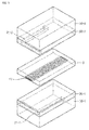
- FIGS. 1 to 3 illustrate a structure of a microplasma jet device according to an embodiment of the present invention, where FIG. 1 is a transparent perspective view illustrating the microplasma jet device according to the present embodiment, FIG. 2 is a cross-sectional view illustrating the microplasma jet device according to the present embodiment, and FIG. 3 is a transparent exploded perspective view illustrating the microplasma jet device according to the present embodiment.
- the microplasma jet device includes a channel layer 10 having a plurality of microfluidic channels 11arranged in parallel so as to enable a gas for generating plasma to pass therethrough, a first insulating layer 20-1 which is bonded to one surface (a lower surface in the drawing) of the channel layer 10 and in which a first plasma generation electrode 21-1 is formed, a second insulating layer 20-2 which is bonded to another surface (an upper surface in the drawing) of the channel layer 10 and in which a second plasma generation electrode 21-2 is formed, a first substrate 30-1 to which the first insulating layer 20-1 is fixed, and a second substrate 30-2 to which the second insulating layer 20-2 is fixed.
- the channel layer 10 in which the plurality of microfluidic channels 11 are formed may be formed using a micromachining process.
- the plurality of microfluidic channels, each of which having a desired small size, may be formed using the micromachining process.
- the formation of the channel layer 10 will be described with reference to FIG. 4 .
- the channel layer 10 is preferably made of a polymer-based material that can be used for insulating and can be processed as a mold, and here, the polymer-based material may include, for example, polydimethylsiloxane (PDMS).
- PDMS polydimethylsiloxane
- the present invention is not limited thereto, and the number thereof may be, for example, several to several tens. Further, the microfluidic channels 11 of a required number may be implemented according to an area to be processed.
- a width of the single microfluidic channel may range from about 100 ⁇ m to 500 ⁇ m, and a height thereof may be about 100 ⁇ m. However, there is no specific limitation on a size of the microfluidic channel, and the size may range, for example, from several tens of ⁇ m to several hundreds of ⁇ m.
- a distance between the microfluidic channels may be two times the width, but there is no specific limitation thereon, and the distance may be several times or several hundred times the width of the channel.
- the microfluidic channels 11 are formed on a lower side of the channel layer 10 based on the drawings, the microfluidic channels 11 may be formed on an upper side of the channel layer 10. Referring to FIGS. 1 and 3 , the microfluidic channels 11 at one side (a right side in the drawing) corresponds to inlets of the gas for generating plasma, and the microfluidic channels 11 at another side (a left side in the drawing) corresponds to outlets of the gas for generating plasma.
- the first insulating layer 20-1 and the second insulating layer 20-2 serve to insulate the first plasma generation electrode 21-1 and the second plasma generation electrode 21-2 from the microfluidic channels 11 with the channel layer 10.
- the microfluidic channels 11 are insulated from the first plasma generation electrode 21-1 by the first insulating layer 20-1, and are insulated from the second plasma generation electrode 21-2 by the channel layer 10 and the second insulating layer 20-2.
- the first insulating layer 20-1 and the second insulating layer 20-2 may be made of a polymer-based material, and here, the polymer-based material may include, for example, PDMS.
- the first plasma generation electrode 21-1 and the second plasma generation electrode 21-2 may be respectively formed in the first insulating layer 20-1 and the second insulating layer 20-2, and may be formed in a predetermined pattern to be suitable for the generation of plasma.
- the patterns of the first plasma generation electrode 21-1 and the second plasma generation electrode 21-2 may be formed to face each other at portions corresponding to the outlets of the microfluidic channels 11.
- the first plasma generation electrode 21-1 and the second plasma generation electrode 21-2 may be respectively formed on surfaces opposite to surfaces in which the first insulating layer 20-1 and the second insulating layer 20-2 are bonded to the channel layer 10 so as to be insulated from the microfluidic channels 11 by the first insulating layer 20-1 and the second insulating layer 20-2.
- the first plasma generation electrode 21-1 and the second plasma generation electrode 21-2 may be formed, for example, by nickel plating.
- the first substrate 30-1 and the second substrate 30-2 respectively fix the first insulating layer 20-1 and the second insulating layer 20-2, respectively fix the first plasma generation electrode 21-1 and the second plasma generation electrode 21-2, and also serve to respectively insulate the first plasma generation electrode 21-1 and the second plasma generation electrode 21-2 from the outside.
- the first substrate 30-1 and the second substrate 30-2 may be, for example, a glass substrate.
- An operating principle of the microplasma jet device is as follows.
- the gas for generating plasma injected into the inlets of the microfluidic channels 11 is ionized by an electric field formed by the first plasma generation electrode 21-1 and the second plasma generation electrode 21-2 while passing through the microfluidic channels 11, and thus plasma is generated.
- the generated plasma is pushed by the gas entering the microfluidic channels 11, and is jetted through the outlets of the microfluidic channels 11.
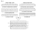
- FIG. 4 is a view illustrating a method of manufacturing a microplasma jet device according to an embodiment of the present invention.
- the method of manufacturing the microplasma jet device mainly includes forming a channel layer 10 in which microfluidic channels 11 are formed, forming an insulating layer 20-1 or 20-2, in which a plasma generation electrode 21-1 or 21-2 are formed, and a substrate 30-1 or 30-2 (hereinafter, referred to as an electrode part), and bonding the channel layer 10 to the electrode parts.
- the forming of the channel layer 10 is as follows.
- a mold is formed by patterning a photosensitizer on one surface of a substrate (for example, a silicon substrate) so as to correspond to a shape of each of the microfluidic channels to be formed (a).
- a channel layer is formed by pouring a polymer solution into the formed mold and curing the polymer solution (b).
- the polymer solution may include a PDMS solution.
- the channel layer in which the microfluidic channels are formed is obtained by separating the cured polymer from the mold (c).
- the forming of the electrode parts is as follows. Since an electrode part bonded to a top of the channel layer 10 and an electrode part bonded to a bottom of the channel layer 10 are typically symmetrical and processes of forming the electrode parts are substantially the same, only the process of forming a single electrode part will be described.
- a seed layer is patterned on one surface of a substrate (for example, the glass substrate) so as to correspond to a pattern of each of the plasma generation electrodes to be formed (d).
- the seed layer may be formed by, for example, depositing titanium or gold using an electroplating method, and for example, a photosensitizer and an etching solution may be used in the patterning of the seed layer.
- the plasma generation electrodes are formed by plating the patterned seed layer (e).
- the plasma generation electrodes may be formed by electroplating the seed layer with nickel.
- an insulating layer is formed by polymer coating a surface of the substrate, in which the plasma generation electrodes are formed, so that all of the plasma generation electrodes are covered (f).
- the microplasma jet device according to the embodiment of the present invention is completed. That is, the first insulating layer 20-1 is bonded to a lower surface of the channel layer 10, and the second insulating layer 20-2 is bonded to an upper surface of the channel layer 10.
- the channel layer 10 and the insulating layers 20-1 and 20-2 are to be in close contact with each other and are heated to a determined temperature (for example, about 1500 °C) for a predetermined time (for example, about 15 minutes), the channel layer 10 and the insulating layers 20-1 and 20-2 may be bonded to each other.
- a microplasma jet module having a laminated structure may be formed by stacking two or more of the microplasma jet devices according to the embodiment of the present. For example, this is because the channel layer and the insulating layer, which are made of a polymer-based material, are easily bonded to each other. According to the embodiment of the present invention, since a size of the module may be increased by as much as desired by stacking the microplasma jet devices, a microplasma jet module that can process as large an area as desired at one time may be implemented.
- FIGS. 5 and 6 illustrate a structure of a laminated microplasma jet module according to an embodiment of the present invention, where FIG. 5 is a transparent perspective view illustrating the laminated microplasma jet module according to the present embodiment and FIG. 6 is a cross-sectional view illustrating the laminated microplasma jet module according to the present embodiment.
- the laminated microplasma jet module includes channel layers 10 having a plurality of microfluidic channels 11arranged in parallel so as to enable a gas for generating plasma to pass therethrough, two microplasma jet devices each including a first insulating layer 20-1 which is bonded to one surface (a lower surface in the drawing) of the channel layer 10 and in which a first plasma generation electrode 21-1 is formed and a second insulating layer 20-2 which is bonded to another surface (an upper surface in the drawing) of the channel layer 10 and in which a second plasma generation electrode 21-2 is formed, wherein the two microplasma jet devices are laminated by interposing an intermediate substrate 30-3 therebetween, a first substrate 30-1 to which the first insulating layer 20-1 of a lower microplasma jet device is fixed, and a second substrate 30-2 to which the second insulating layer 20-2 of an upper microplasma jet device is fixed.
- microplasma jet devices being laminated are described as an example, two or more of the microplasma jet devices may be laminated.
- a process of forming the laminated microplasma jet module of FIGS. 5 and 6 is as follows.
- Two channel layers 10 may be formed through the above-described process of forming the channel layer.
- electrode part two electrode parts, that is, a lower electrode part including the first substrate 30-1, the first plasma generation electrode 21-1, and the first insulating layer 20-1, and an upper electrode part including the second substrate 30-2, the second plasma generation electrode 21-2, and the second insulating layer 20-2, may be formed.
- the plasma generation electrodes 21-1 and 21-2 and the insulating layers 20-1 and 20-2 are respectively formed on both side surfaces of the intermediate substrate 30-3. Therefore, an intermediate electrode part including the intermediate substrate 30-3 and the plasma generation electrodes 21-1 and 21-2 and the insulating layers 20-1 and 20-2 which are formed on the both side surfaces of the intermediate substrate 30-3 may be formed through a process similar to the above-described process of forming the electrode part.
- the intermediate electrode part may be formed through a process in which the above-described process of forming the electrode part is slightly modified, that is, through a process of respectively forming the plasma generation electrode and the insulating layer on both side surfaces of the substrate.
- the laminated microplasma jet module according to the present embodiment is completed.
Landscapes
- Physics & Mathematics (AREA)
- Engineering & Computer Science (AREA)
- Plasma & Fusion (AREA)
- Spectroscopy & Molecular Physics (AREA)
- Chemical & Material Sciences (AREA)
- Analytical Chemistry (AREA)
- Micromachines (AREA)
- Physical Or Chemical Processes And Apparatus (AREA)
Abstract
Description
- The present invention relates to a plasma jet device, and more particularly, to a microplasma jet device capable of processing a large area, a laminated microplasma jet module, and a method of manufacturing the microplasma jet device.
- Plasma has been applied in various fields such as the semiconductor industry, the display industry, and for surface modification of materials. Recently, attempts to apply plasma to a bio-medical technology or surface processing of a material such as plastic or fiber have been made. However, in these applications, since an object material that should be treated by the plasma is sensitive to heat, a glow discharge, which is low-temperature plasma, should be used. Because glow discharge is very unstable at normal pressure, a glow-to-arc transition (GAT) in which the glow discharge is transitioned to an arc discharge, which is high-temperature plasma, is likely to occur.
- The GAT occurs by heat generated while the plasma is generated, and research on microplasma generated by reducing the capacity of the plasma has been progressing as a method of preventing the GAT.
- Conventionally, devices for generating microplasma cause discharge using needles or tubes which are mechanically processed. However, since there is a limit in reducing the size thereof through the mechanical processing and the plasma is generated using a single tube or needle, an area that can be processed at one time is limited.
- The present invention is directed to providing a microplasma jet device capable of processing a larger area, a laminated microplasma jet module, and a method of manufacturing the microplasma jet device.
- One aspect of the present invention provides a microplasma jet device including: a channel layer having a plurality of microfluidic channels arranged in parallel so as to enable a gas for generating plasma to pass therethrough; a first insulating layer bonded to one surface of the channel layer and in which a first plasma generation electrode is formed; and a second insulating layer bonded to another surface of the channel layer and in which a second plasma generation electrode is formed.
- The microplasma jet device may further include a first substrate to which the first insulating layer is fixed and a second substrate to which the second insulating layer is fixed.
- The channel layer may be made of a polymer-based material.
- The polymer-based material may include polydimethylsiloxane (PDMS).
- The first insulating layer and the second insulating layer may be made of a polymer-based material.
- The first plasma generation electrode and the second plasma generation electrode may be formed by nickel plating.
- The plurality of microfluidic channels may be insulated from the first plasma generation electrode and the second plasma generation electrode by the first insulating layer and the second insulating layer.
- Another aspect of the present invention provides a microplasma jet module having a structure in which two or more of the microplasma jet devices are laminated by interposing a substrate therebetween.
- Still another aspect of the present invention provides a method of manufacturing the microplasma jet device including: forming a mold by patterning a photosensitizer on one surface of a substrate to correspond to a plurality of microfluidic channels to be formed; forming a channel layer by pouring a polymer solution into the mold and curing the polymer solution; separating the channel layer from the mold; patterning a seed layer on one surface of a first substrate to correspond to a pattern of a first plasma generation electrode to be formed; forming the first plasma generation electrode by plating the seed layer; forming a first insulating layer by polymer coating a surface of the first substrate, in which the first plasma generation electrode is formed; patterning a seed layer on one surface of a second substrate to correspond to a pattern of a second plasma generation electrode to be formed; forming the second plasma generation electrode by plating the seed layer; forming a second insulating layer by polymer coating a surface of the second substrate, in which the second plasma generation electrode is formed; and bonding the first insulating layer, the channel layer, and the second insulating layer to each other.
- The polymer solution may include a PDMS solution.
- The patterning of the seed layer may include depositing titanium or gold.
- The forming of the first plasma generation electrode or the forming of the second plasma generation electrode may include electroplating the seed layer with nickel.
- According to the present invention, a microplasma jet device capable of processing a larger area, a laminated microplasma jet module, and a method of manufacturing the microplasma jet device are provided.
-
-
FIG. 1 is a transparent perspective view illustrating a microplasma jet device according to an embodiment of the present invention. -
FIG. 2 is a cross-sectional view illustrating a microplasma jet device according to an embodiment of the present invention. -
FIG. 3 is a transparent exploded perspective view illustrating a microplasma jet device according to an embodiment of the present invention. -
FIG. 4 is a view illustrating a method of manufacturing a microplasma jet device according to an embodiment of the present invention. -
FIG. 5 is a transparent perspective view illustrating a laminated microplasma jet module according to an embodiment of the present invention. -
FIG. 6 is a cross-sectional view illustrating a laminated microplasma jet module according to an embodiment of the present invention. - Hereinafter, exemplary embodiments of the invention will be described in detail with reference to the accompanying drawings. Like reference numerals in the drawings and descriptions denote like devices, and thus the description thereof will be omitted. Further, when it is determined that detailed explanations of related well-known functions or configurations unnecessarily obscure gist of the embodiments, the detailed description thereof will be omitted.
-
FIGS. 1 to 3 illustrate a structure of a microplasma jet device according to an embodiment of the present invention, whereFIG. 1 is a transparent perspective view illustrating the microplasma jet device according to the present embodiment,FIG. 2 is a cross-sectional view illustrating the microplasma jet device according to the present embodiment, andFIG. 3 is a transparent exploded perspective view illustrating the microplasma jet device according to the present embodiment. - Referring to
FIGS. 1 to 3 , the microplasma jet device according to the present embodiment includes achannel layer 10 having a plurality of microfluidic channels 11arranged in parallel so as to enable a gas for generating plasma to pass therethrough, a first insulating layer 20-1 which is bonded to one surface (a lower surface in the drawing) of thechannel layer 10 and in which a first plasma generation electrode 21-1 is formed, a second insulating layer 20-2 which is bonded to another surface (an upper surface in the drawing) of thechannel layer 10 and in which a second plasma generation electrode 21-2 is formed, a first substrate 30-1 to which the first insulating layer 20-1 is fixed, and a second substrate 30-2 to which the second insulating layer 20-2 is fixed. - In the embodiment of the present invention, the
channel layer 10 in which the plurality ofmicrofluidic channels 11 are formed may be formed using a micromachining process. The plurality of microfluidic channels, each of which having a desired small size, may be formed using the micromachining process. The formation of thechannel layer 10 will be described with reference toFIG. 4 . Thechannel layer 10 is preferably made of a polymer-based material that can be used for insulating and can be processed as a mold, and here, the polymer-based material may include, for example, polydimethylsiloxane (PDMS). - Referring to
FIG. 2 , although it is illustrated that the number of themicrofluidic channels 11 formed in asingle channel layer 10 is, for example, 8, the present invention is not limited thereto, and the number thereof may be, for example, several to several tens. Further, themicrofluidic channels 11 of a required number may be implemented according to an area to be processed. - A width of the single microfluidic channel may range from about 100 µm to 500 µm, and a height thereof may be about 100 µm. However, there is no specific limitation on a size of the microfluidic channel, and the size may range, for example, from several tens of µm to several hundreds of µm. A distance between the microfluidic channels may be two times the width, but there is no specific limitation thereon, and the distance may be several times or several hundred times the width of the channel.
- Although it is illustrated that the
microfluidic channels 11 are formed on a lower side of thechannel layer 10 based on the drawings, themicrofluidic channels 11 may be formed on an upper side of thechannel layer 10. Referring toFIGS. 1 and3 , themicrofluidic channels 11 at one side (a right side in the drawing) corresponds to inlets of the gas for generating plasma, and themicrofluidic channels 11 at another side (a left side in the drawing) corresponds to outlets of the gas for generating plasma. - The first insulating layer 20-1 and the second insulating layer 20-2 serve to insulate the first plasma generation electrode 21-1 and the second plasma generation electrode 21-2 from the
microfluidic channels 11 with thechannel layer 10. Specifically, themicrofluidic channels 11 are insulated from the first plasma generation electrode 21-1 by the first insulating layer 20-1, and are insulated from the second plasma generation electrode 21-2 by thechannel layer 10 and the second insulating layer 20-2. - The first insulating layer 20-1 and the second insulating layer 20-2 may be made of a polymer-based material, and here, the polymer-based material may include, for example, PDMS.
- The first plasma generation electrode 21-1 and the second plasma generation electrode 21-2 may be respectively formed in the first insulating layer 20-1 and the second insulating layer 20-2, and may be formed in a predetermined pattern to be suitable for the generation of plasma. For example, the patterns of the first plasma generation electrode 21-1 and the second plasma generation electrode 21-2 may be formed to face each other at portions corresponding to the outlets of the
microfluidic channels 11. - The first plasma generation electrode 21-1 and the second plasma generation electrode 21-2 may be respectively formed on surfaces opposite to surfaces in which the first insulating layer 20-1 and the second insulating layer 20-2 are bonded to the
channel layer 10 so as to be insulated from themicrofluidic channels 11 by the first insulating layer 20-1 and the second insulating layer 20-2. The first plasma generation electrode 21-1 and the second plasma generation electrode 21-2 may be formed, for example, by nickel plating. - The first substrate 30-1 and the second substrate 30-2 respectively fix the first insulating layer 20-1 and the second insulating layer 20-2, respectively fix the first plasma generation electrode 21-1 and the second plasma generation electrode 21-2, and also serve to respectively insulate the first plasma generation electrode 21-1 and the second plasma generation electrode 21-2 from the outside. The first substrate 30-1 and the second substrate 30-2 may be, for example, a glass substrate.
- An operating principle of the microplasma jet device according to the present embodiment is as follows. The gas for generating plasma injected into the inlets of the
microfluidic channels 11 is ionized by an electric field formed by the first plasma generation electrode 21-1 and the second plasma generation electrode 21-2 while passing through themicrofluidic channels 11, and thus plasma is generated. The generated plasma is pushed by the gas entering themicrofluidic channels 11, and is jetted through the outlets of themicrofluidic channels 11. -
FIG. 4 is a view illustrating a method of manufacturing a microplasma jet device according to an embodiment of the present invention. - The method of manufacturing the microplasma jet device according to the present embodiment mainly includes forming a
channel layer 10 in whichmicrofluidic channels 11 are formed, forming an insulating layer 20-1 or 20-2, in which a plasma generation electrode 21-1 or 21-2 are formed, and a substrate 30-1 or 30-2 (hereinafter, referred to as an electrode part), and bonding thechannel layer 10 to the electrode parts. - The forming of the
channel layer 10 is as follows. A mold is formed by patterning a photosensitizer on one surface of a substrate (for example, a silicon substrate) so as to correspond to a shape of each of the microfluidic channels to be formed (a). Then, a channel layer is formed by pouring a polymer solution into the formed mold and curing the polymer solution (b). Here, the polymer solution may include a PDMS solution. Next, the channel layer in which the microfluidic channels are formed is obtained by separating the cured polymer from the mold (c). - The forming of the electrode parts is as follows. Since an electrode part bonded to a top of the
channel layer 10 and an electrode part bonded to a bottom of thechannel layer 10 are typically symmetrical and processes of forming the electrode parts are substantially the same, only the process of forming a single electrode part will be described. - A seed layer is patterned on one surface of a substrate (for example, the glass substrate) so as to correspond to a pattern of each of the plasma generation electrodes to be formed (d). Here, the seed layer may be formed by, for example, depositing titanium or gold using an electroplating method, and for example, a photosensitizer and an etching solution may be used in the patterning of the seed layer. Next, the plasma generation electrodes are formed by plating the patterned seed layer (e). Here, the plasma generation electrodes may be formed by electroplating the seed layer with nickel. Next, an insulating layer is formed by polymer coating a surface of the substrate, in which the plasma generation electrodes are formed, so that all of the plasma generation electrodes are covered (f). Through the above-described processes such as (d), (e), and (f), the electrode part including the substrate 30-1 or 30-2, the plasma generation electrode 21-1 or 21-2, and the insulating layer 20-1 or 20-2 is formed.
- Then, as the channel layer and the electrode parts which are formed in the above-described manner are bonded to each other, the microplasma jet device according to the embodiment of the present invention is completed. That is, the first insulating layer 20-1 is bonded to a lower surface of the
channel layer 10, and the second insulating layer 20-2 is bonded to an upper surface of thechannel layer 10. In this case, as thechannel layer 10 and the insulating layers 20-1 and 20-2 are to be in close contact with each other and are heated to a determined temperature (for example, about 1500 °C) for a predetermined time (for example, about 15 minutes), thechannel layer 10 and the insulating layers 20-1 and 20-2 may be bonded to each other. - A microplasma jet module having a laminated structure may be formed by stacking two or more of the microplasma jet devices according to the embodiment of the present. For example, this is because the channel layer and the insulating layer, which are made of a polymer-based material, are easily bonded to each other. According to the embodiment of the present invention, since a size of the module may be increased by as much as desired by stacking the microplasma jet devices, a microplasma jet module that can process as large an area as desired at one time may be implemented.
-
FIGS. 5 and6 illustrate a structure of a laminated microplasma jet module according to an embodiment of the present invention, whereFIG. 5 is a transparent perspective view illustrating the laminated microplasma jet module according to the present embodiment andFIG. 6 is a cross-sectional view illustrating the laminated microplasma jet module according to the present embodiment. - Referring to
FIGS. 5 and6 , the laminated microplasma jet module according to the present embodiment includes channel layers 10 having a plurality of microfluidic channels 11arranged in parallel so as to enable a gas for generating plasma to pass therethrough, two microplasma jet devices each including a first insulating layer 20-1 which is bonded to one surface (a lower surface in the drawing) of thechannel layer 10 and in which a first plasma generation electrode 21-1 is formed and a second insulating layer 20-2 which is bonded to another surface (an upper surface in the drawing) of thechannel layer 10 and in which a second plasma generation electrode 21-2 is formed, wherein the two microplasma jet devices are laminated by interposing an intermediate substrate 30-3 therebetween, a first substrate 30-1 to which the first insulating layer 20-1 of a lower microplasma jet device is fixed, and a second substrate 30-2 to which the second insulating layer 20-2 of an upper microplasma jet device is fixed. - In the present embodiment, although two of the microplasma jet devices being laminated is described as an example, two or more of the microplasma jet devices may be laminated.
- A process of forming the laminated microplasma jet module of
FIGS. 5 and6 is as follows. - Two channel layers 10 may be formed through the above-described process of forming the channel layer.
- Further, through the above-described process of forming electrode part, two electrode parts, that is, a lower electrode part including the first substrate 30-1, the first plasma generation electrode 21-1, and the first insulating layer 20-1, and an upper electrode part including the second substrate 30-2, the second plasma generation electrode 21-2, and the second insulating layer 20-2, may be formed.
- Referring to
FIGS. 5 and6 , the plasma generation electrodes 21-1 and 21-2 and the insulating layers 20-1 and 20-2 are respectively formed on both side surfaces of the intermediate substrate 30-3. Therefore, an intermediate electrode part including the intermediate substrate 30-3 and the plasma generation electrodes 21-1 and 21-2 and the insulating layers 20-1 and 20-2 which are formed on the both side surfaces of the intermediate substrate 30-3 may be formed through a process similar to the above-described process of forming the electrode part. Since the above-described process of forming the electrode part is a process of forming the plasma generation electrode and the insulating layer on only one side surface of the substrate, the intermediate electrode part may be formed through a process in which the above-described process of forming the electrode part is slightly modified, that is, through a process of respectively forming the plasma generation electrode and the insulating layer on both side surfaces of the substrate. - When the two channel layers, the upper and lower electrode parts, and the intermediate electrode part, which are formed in this manner, are bonded in an order illustrated in
FIGS. 5 and6 , the laminated microplasma jet module according to the present embodiment is completed. - While the present invention has been particularly described with reference to exemplary embodiments, it should be understood by those skilled in the art that various changes in form and details may be made without departing from the spirit and scope of the present invention. Therefore, the exemplary embodiments should be considered in a descriptive sense only and not for purposes of limitation. The scope of the invention is defined not by the detailed description of the invention but by the appended claims, and encompasses all modifications and equivalents that fall within the scope of the appended claims and are construed as being included in the present invention.
Claims (12)
- A microplasma jet device, comprising:a channel layer having a plurality of microfluidic channels arranged in parallel so as to enable a gas for generating plasma to pass therethrough, are formed;a first insulating layer bonded to one surface of the channel layer and in which a first plasma generation electrode is formed; anda second insulating layer bonded to another surface of the channel layer and in which a second plasma generation electrode is formed.
- The device of claim 1, further comprising:a first substrate to which the first insulating layer is fixed; anda second substrate to which the second insulating layer is fixed.
- The device of claim 1, wherein the channel layer is made of a polymer-based material.
- The device of claim 3, wherein the polymer-based material includes polydimethylsiloxane (PDMS).
- The device of claim 1, wherein the first insulating layer and the second insulating layer is made of a polymer-based material.
- The device of claim 1, wherein the first plasma generation electrode and the second plasma generation electrode is formed by nickel plating.
- The device of claim 1, wherein the plurality of microfluidic channels are insulated from the first plasma generation electrode and the second plasma generation electrode by the first insulating layer and the second insulating layer.
- A microplasma jet module having a structure in which two or more of the microplasma jet devices according to claim 1 are laminated by interposing a substrate therebetween.
- A method of manufacturing a microplasma jet device, the method comprising:forming a mold by patterning a photosensitizer on one surface of a substrate to correspond to a plurality of microfluidic channels to be formed;forming a channel layer by pouring a polymer solution into the mold and curing the polymer solution;separating the channel layer from the mold;patterning a seed layer on one surface of a first substrate to correspond to a pattern of a first plasma generation electrode to be formed;forming the first plasma generation electrode by plating the seed layer;forming a first insulating layer by polymer coating a surface of the first substrate, in which the first plasma generation electrode is formed;patterning a seed layer on one surface of a second substrate to correspond to a pattern of a second plasma generation electrode to be formed;forming the second plasma generation electrode by plating the seed layer;forming a second insulating layer by polymer coating a surface of the second substrate, in which the second plasma generation electrode is formed; andbonding the first insulating layer, the channel layer, and the second insulating layer to each other.
- The method of claim 9, wherein the polymer solution includes a PDMS solution.
- The method of claim 9, wherein the patterning of the seed layer includes depositing titanium or gold.
- The method of claim 9, wherein the forming of the first plasma generation electrode or the forming of the second plasma generation electrode includes electroplating the seed layer with nickel.
Applications Claiming Priority (3)
| Application Number | Priority Date | Filing Date | Title |
|---|---|---|---|
| KR20130118027 | 2013-10-02 | ||
| KR1020140122736A KR101594464B1 (en) | 2013-10-02 | 2014-09-16 | Micro plasma jet device, laminate type micro plasma jet module and manufacturing method thereof |
| PCT/KR2014/009260 WO2015050376A1 (en) | 2013-10-02 | 2014-10-01 | Microplasma spray element, laminated microplasma spray module and method for manufacturing microplasma spray element |
Publications (3)
| Publication Number | Publication Date |
|---|---|
| EP3054748A1 true EP3054748A1 (en) | 2016-08-10 |
| EP3054748A4 EP3054748A4 (en) | 2017-05-24 |
| EP3054748B1 EP3054748B1 (en) | 2021-05-12 |
Family
ID=53029882
Family Applications (1)
| Application Number | Title | Priority Date | Filing Date |
|---|---|---|---|
| EP14850871.6A Active EP3054748B1 (en) | 2013-10-02 | 2014-10-01 | Method for manufacturing microplasma jet device |
Country Status (3)
| Country | Link |
|---|---|
| US (1) | US20160219687A1 (en) |
| EP (1) | EP3054748B1 (en) |
| KR (1) | KR101594464B1 (en) |
Family Cites Families (10)
| Publication number | Priority date | Publication date | Assignee | Title |
|---|---|---|---|---|
| DE19826418C2 (en) * | 1998-06-16 | 2003-07-31 | Horst Schmidt-Boecking | Device for generating a plasma and a manufacturing method for the device and use of the device |
| WO2001027969A1 (en) * | 1999-10-12 | 2001-04-19 | Wisconsin Alumni Research Foundation | Method and apparatus for etching and deposition using micro-plasmas |
| WO2004107825A1 (en) * | 2003-05-30 | 2004-12-09 | Tokyo Electron Limited | Plasma source and plasma processing apparatus |
| JP4925087B2 (en) * | 2005-10-28 | 2012-04-25 | 三菱電機株式会社 | Ozone generator |
| US8497631B2 (en) * | 2006-01-23 | 2013-07-30 | The Board Of Trustees Of The University Of Illinois | Polymer microcavity and microchannel devices and fabrication method |
| JP5081689B2 (en) * | 2008-03-28 | 2012-11-28 | 日本碍子株式会社 | Microplasma jet reactor and microplasma jet generator |
| US8890409B2 (en) * | 2008-05-14 | 2014-11-18 | The Board Of Trustees Of The University Of Illnois | Microcavity and microchannel plasma device arrays in a single, unitary sheet |
| KR101001477B1 (en) * | 2009-02-27 | 2010-12-14 | 아주대학교산학협력단 | Atmospheric Low Temperature Micro Plasma Injection Apparatus for Bio-Medical Applications |
| WO2012178177A2 (en) * | 2011-06-24 | 2012-12-27 | The Board Of Trustees Of The University Of Illinois | Microplasma jet devices, arrays, medical devices and methods |
| KR101292268B1 (en) * | 2011-08-29 | 2013-08-01 | 한림대학교 산학협력단 | Parallel driving micro plasma devices for treatment of wound area |
-
2014
- 2014-09-16 KR KR1020140122736A patent/KR101594464B1/en active Active
- 2014-10-01 EP EP14850871.6A patent/EP3054748B1/en active Active
- 2014-10-01 US US15/025,842 patent/US20160219687A1/en not_active Abandoned
Also Published As
| Publication number | Publication date |
|---|---|
| US20160219687A1 (en) | 2016-07-28 |
| EP3054748A4 (en) | 2017-05-24 |
| EP3054748B1 (en) | 2021-05-12 |
| KR20150039678A (en) | 2015-04-13 |
| KR101594464B1 (en) | 2016-02-18 |
Similar Documents
| Publication | Publication Date | Title |
|---|---|---|
| CN105470343B (en) | Optically pumped sensor or fiducial with mold-package cavity | |
| US9740111B2 (en) | Electrostatic carrier for handling substrates for processing | |
| KR101905158B1 (en) | Locally heated multi-zone substrate support | |
| CN107305915B (en) | Electron-programmable magnetic transfer module and transfer method for electronic components | |
| TWI697407B (en) | Substrate bonding method and micro wafer manufacturing method | |
| TWI590411B (en) | Apparatus and method for shielding and biasing in a microelectromechanical system component packaged by an active circuit system | |
| JP2019536294A (en) | Flexible connector | |
| EP3221049A1 (en) | Microbubble generator device, systems and method to fabricate | |
| CN107381495B (en) | A MEMS micro-hot plate and its manufacturing method | |
| EP2401896B1 (en) | Atmospheric low-temperature micro plasma jet device for bio-medical application | |
| US20090289313A1 (en) | Micro electric mechanical system device and method of producing the same | |
| EP3054748B1 (en) | Method for manufacturing microplasma jet device | |
| US20150044424A1 (en) | Bottom electrode and manufacturing method thereof | |
| JP5785862B2 (en) | Electrostatic chuck and manufacturing method thereof, substrate temperature control fixing device | |
| JP2011014868A (en) | Inductive element having gap and fabrication method thereof | |
| SE538311C2 (en) | Thin covering structure for MEMS devices | |
| KR101756847B1 (en) | Wearable patch type hybrid substrate and a method for fabricating the same | |
| US20160118737A1 (en) | Fluid Pressure Activated Electrical Contact Devices and Methods | |
| KR101086006B1 (en) | Probe and probe unit manufacturing method and probe unit | |
| WO2015050376A1 (en) | Microplasma spray element, laminated microplasma spray module and method for manufacturing microplasma spray element | |
| US20040121619A1 (en) | Multipoint minute electrode, device for measuring a living organism voltage, method for fabricating the multipoint minute electrode, and method for fabricating the living organism voltage-measuring device | |
| KR101829227B1 (en) | Electrostatic chuck improved in electrostatic plate structure | |
| KR101816483B1 (en) | Heating film and its making method | |
| CN208749522U (en) | Gas delivery device | |
| TW202035275A (en) | Manufacturing method of micro-electromechanical system pump |
Legal Events
| Date | Code | Title | Description |
|---|---|---|---|
| PUAI | Public reference made under article 153(3) epc to a published international application that has entered the european phase |
Free format text: ORIGINAL CODE: 0009012 |
|
| 17P | Request for examination filed |
Effective date: 20160502 |
|
| AK | Designated contracting states |
Kind code of ref document: A1 Designated state(s): AL AT BE BG CH CY CZ DE DK EE ES FI FR GB GR HR HU IE IS IT LI LT LU LV MC MK MT NL NO PL PT RO RS SE SI SK SM TR |
|
| AX | Request for extension of the european patent |
Extension state: BA ME |
|
| DAX | Request for extension of the european patent (deleted) | ||
| A4 | Supplementary search report drawn up and despatched |
Effective date: 20170424 |
|
| RIC1 | Information provided on ipc code assigned before grant |
Ipc: H05H 1/34 20060101AFI20170418BHEP Ipc: H05H 1/24 20060101ALI20170418BHEP |
|
| STAA | Information on the status of an ep patent application or granted ep patent |
Free format text: STATUS: EXAMINATION IS IN PROGRESS |
|
| 17Q | First examination report despatched |
Effective date: 20190313 |
|
| GRAP | Despatch of communication of intention to grant a patent |
Free format text: ORIGINAL CODE: EPIDOSNIGR1 |
|
| STAA | Information on the status of an ep patent application or granted ep patent |
Free format text: STATUS: GRANT OF PATENT IS INTENDED |
|
| INTG | Intention to grant announced |
Effective date: 20201207 |
|
| GRAS | Grant fee paid |
Free format text: ORIGINAL CODE: EPIDOSNIGR3 |
|
| GRAA | (expected) grant |
Free format text: ORIGINAL CODE: 0009210 |
|
| STAA | Information on the status of an ep patent application or granted ep patent |
Free format text: STATUS: THE PATENT HAS BEEN GRANTED |
|
| AK | Designated contracting states |
Kind code of ref document: B1 Designated state(s): AL AT BE BG CH CY CZ DE DK EE ES FI FR GB GR HR HU IE IS IT LI LT LU LV MC MK MT NL NO PL PT RO RS SE SI SK SM TR |
|
| REG | Reference to a national code |
Ref country code: GB Ref legal event code: FG4D |
|
| REG | Reference to a national code |
Ref country code: CH Ref legal event code: EP |
|
| REG | Reference to a national code |
Ref country code: DE Ref legal event code: R096 Ref document number: 602014077457 Country of ref document: DE |
|
| REG | Reference to a national code |
Ref country code: IE Ref legal event code: FG4D |
|
| REG | Reference to a national code |
Ref country code: AT Ref legal event code: REF Ref document number: 1393060 Country of ref document: AT Kind code of ref document: T Effective date: 20210615 |
|
| REG | Reference to a national code |
Ref country code: LT Ref legal event code: MG9D |
|
| REG | Reference to a national code |
Ref country code: AT Ref legal event code: MK05 Ref document number: 1393060 Country of ref document: AT Kind code of ref document: T Effective date: 20210512 |
|
| REG | Reference to a national code |
Ref country code: NL Ref legal event code: MP Effective date: 20210512 |
|
| PG25 | Lapsed in a contracting state [announced via postgrant information from national office to epo] |
Ref country code: FI Free format text: LAPSE BECAUSE OF FAILURE TO SUBMIT A TRANSLATION OF THE DESCRIPTION OR TO PAY THE FEE WITHIN THE PRESCRIBED TIME-LIMIT Effective date: 20210512 Ref country code: LT Free format text: LAPSE BECAUSE OF FAILURE TO SUBMIT A TRANSLATION OF THE DESCRIPTION OR TO PAY THE FEE WITHIN THE PRESCRIBED TIME-LIMIT Effective date: 20210512 Ref country code: BG Free format text: LAPSE BECAUSE OF FAILURE TO SUBMIT A TRANSLATION OF THE DESCRIPTION OR TO PAY THE FEE WITHIN THE PRESCRIBED TIME-LIMIT Effective date: 20210812 Ref country code: AT Free format text: LAPSE BECAUSE OF FAILURE TO SUBMIT A TRANSLATION OF THE DESCRIPTION OR TO PAY THE FEE WITHIN THE PRESCRIBED TIME-LIMIT Effective date: 20210512 Ref country code: HR Free format text: LAPSE BECAUSE OF FAILURE TO SUBMIT A TRANSLATION OF THE DESCRIPTION OR TO PAY THE FEE WITHIN THE PRESCRIBED TIME-LIMIT Effective date: 20210512 |
|
| PG25 | Lapsed in a contracting state [announced via postgrant information from national office to epo] |
Ref country code: PL Free format text: LAPSE BECAUSE OF FAILURE TO SUBMIT A TRANSLATION OF THE DESCRIPTION OR TO PAY THE FEE WITHIN THE PRESCRIBED TIME-LIMIT Effective date: 20210512 Ref country code: PT Free format text: LAPSE BECAUSE OF FAILURE TO SUBMIT A TRANSLATION OF THE DESCRIPTION OR TO PAY THE FEE WITHIN THE PRESCRIBED TIME-LIMIT Effective date: 20210913 Ref country code: NO Free format text: LAPSE BECAUSE OF FAILURE TO SUBMIT A TRANSLATION OF THE DESCRIPTION OR TO PAY THE FEE WITHIN THE PRESCRIBED TIME-LIMIT Effective date: 20210812 Ref country code: ES Free format text: LAPSE BECAUSE OF FAILURE TO SUBMIT A TRANSLATION OF THE DESCRIPTION OR TO PAY THE FEE WITHIN THE PRESCRIBED TIME-LIMIT Effective date: 20210512 Ref country code: RS Free format text: LAPSE BECAUSE OF FAILURE TO SUBMIT A TRANSLATION OF THE DESCRIPTION OR TO PAY THE FEE WITHIN THE PRESCRIBED TIME-LIMIT Effective date: 20210512 Ref country code: SE Free format text: LAPSE BECAUSE OF FAILURE TO SUBMIT A TRANSLATION OF THE DESCRIPTION OR TO PAY THE FEE WITHIN THE PRESCRIBED TIME-LIMIT Effective date: 20210512 Ref country code: GR Free format text: LAPSE BECAUSE OF FAILURE TO SUBMIT A TRANSLATION OF THE DESCRIPTION OR TO PAY THE FEE WITHIN THE PRESCRIBED TIME-LIMIT Effective date: 20210813 Ref country code: IS Free format text: LAPSE BECAUSE OF FAILURE TO SUBMIT A TRANSLATION OF THE DESCRIPTION OR TO PAY THE FEE WITHIN THE PRESCRIBED TIME-LIMIT Effective date: 20210912 Ref country code: LV Free format text: LAPSE BECAUSE OF FAILURE TO SUBMIT A TRANSLATION OF THE DESCRIPTION OR TO PAY THE FEE WITHIN THE PRESCRIBED TIME-LIMIT Effective date: 20210512 |
|
| PG25 | Lapsed in a contracting state [announced via postgrant information from national office to epo] |
Ref country code: NL Free format text: LAPSE BECAUSE OF FAILURE TO SUBMIT A TRANSLATION OF THE DESCRIPTION OR TO PAY THE FEE WITHIN THE PRESCRIBED TIME-LIMIT Effective date: 20210512 |
|
| PG25 | Lapsed in a contracting state [announced via postgrant information from national office to epo] |
Ref country code: SK Free format text: LAPSE BECAUSE OF FAILURE TO SUBMIT A TRANSLATION OF THE DESCRIPTION OR TO PAY THE FEE WITHIN THE PRESCRIBED TIME-LIMIT Effective date: 20210512 Ref country code: SM Free format text: LAPSE BECAUSE OF FAILURE TO SUBMIT A TRANSLATION OF THE DESCRIPTION OR TO PAY THE FEE WITHIN THE PRESCRIBED TIME-LIMIT Effective date: 20210512 Ref country code: CZ Free format text: LAPSE BECAUSE OF FAILURE TO SUBMIT A TRANSLATION OF THE DESCRIPTION OR TO PAY THE FEE WITHIN THE PRESCRIBED TIME-LIMIT Effective date: 20210512 Ref country code: DK Free format text: LAPSE BECAUSE OF FAILURE TO SUBMIT A TRANSLATION OF THE DESCRIPTION OR TO PAY THE FEE WITHIN THE PRESCRIBED TIME-LIMIT Effective date: 20210512 Ref country code: EE Free format text: LAPSE BECAUSE OF FAILURE TO SUBMIT A TRANSLATION OF THE DESCRIPTION OR TO PAY THE FEE WITHIN THE PRESCRIBED TIME-LIMIT Effective date: 20210512 Ref country code: RO Free format text: LAPSE BECAUSE OF FAILURE TO SUBMIT A TRANSLATION OF THE DESCRIPTION OR TO PAY THE FEE WITHIN THE PRESCRIBED TIME-LIMIT Effective date: 20210512 |
|
| REG | Reference to a national code |
Ref country code: DE Ref legal event code: R097 Ref document number: 602014077457 Country of ref document: DE |
|
| PLBE | No opposition filed within time limit |
Free format text: ORIGINAL CODE: 0009261 |
|
| STAA | Information on the status of an ep patent application or granted ep patent |
Free format text: STATUS: NO OPPOSITION FILED WITHIN TIME LIMIT |
|
| 26N | No opposition filed |
Effective date: 20220215 |
|
| REG | Reference to a national code |
Ref country code: CH Ref legal event code: PL |
|
| PG25 | Lapsed in a contracting state [announced via postgrant information from national office to epo] |
Ref country code: IS Free format text: LAPSE BECAUSE OF FAILURE TO SUBMIT A TRANSLATION OF THE DESCRIPTION OR TO PAY THE FEE WITHIN THE PRESCRIBED TIME-LIMIT Effective date: 20210912 Ref country code: AL Free format text: LAPSE BECAUSE OF FAILURE TO SUBMIT A TRANSLATION OF THE DESCRIPTION OR TO PAY THE FEE WITHIN THE PRESCRIBED TIME-LIMIT Effective date: 20210512 |
|
| REG | Reference to a national code |
Ref country code: BE Ref legal event code: MM Effective date: 20211031 |
|
| GBPC | Gb: european patent ceased through non-payment of renewal fee |
Effective date: 20211001 |
|
| PG25 | Lapsed in a contracting state [announced via postgrant information from national office to epo] |
Ref country code: MC Free format text: LAPSE BECAUSE OF FAILURE TO SUBMIT A TRANSLATION OF THE DESCRIPTION OR TO PAY THE FEE WITHIN THE PRESCRIBED TIME-LIMIT Effective date: 20210512 |
|
| PG25 | Lapsed in a contracting state [announced via postgrant information from national office to epo] |
Ref country code: LU Free format text: LAPSE BECAUSE OF NON-PAYMENT OF DUE FEES Effective date: 20211001 Ref country code: IT Free format text: LAPSE BECAUSE OF FAILURE TO SUBMIT A TRANSLATION OF THE DESCRIPTION OR TO PAY THE FEE WITHIN THE PRESCRIBED TIME-LIMIT Effective date: 20210512 Ref country code: GB Free format text: LAPSE BECAUSE OF NON-PAYMENT OF DUE FEES Effective date: 20211001 Ref country code: BE Free format text: LAPSE BECAUSE OF NON-PAYMENT OF DUE FEES Effective date: 20211031 |
|
| PG25 | Lapsed in a contracting state [announced via postgrant information from national office to epo] |
Ref country code: LI Free format text: LAPSE BECAUSE OF NON-PAYMENT OF DUE FEES Effective date: 20211031 Ref country code: CH Free format text: LAPSE BECAUSE OF NON-PAYMENT OF DUE FEES Effective date: 20211031 |
|
| PG25 | Lapsed in a contracting state [announced via postgrant information from national office to epo] |
Ref country code: FR Free format text: LAPSE BECAUSE OF NON-PAYMENT OF DUE FEES Effective date: 20211031 |
|
| PG25 | Lapsed in a contracting state [announced via postgrant information from national office to epo] |
Ref country code: IE Free format text: LAPSE BECAUSE OF NON-PAYMENT OF DUE FEES Effective date: 20211001 |
|
| PG25 | Lapsed in a contracting state [announced via postgrant information from national office to epo] |
Ref country code: HU Free format text: LAPSE BECAUSE OF FAILURE TO SUBMIT A TRANSLATION OF THE DESCRIPTION OR TO PAY THE FEE WITHIN THE PRESCRIBED TIME-LIMIT; INVALID AB INITIO Effective date: 20141001 |
|
| PG25 | Lapsed in a contracting state [announced via postgrant information from national office to epo] |
Ref country code: CY Free format text: LAPSE BECAUSE OF FAILURE TO SUBMIT A TRANSLATION OF THE DESCRIPTION OR TO PAY THE FEE WITHIN THE PRESCRIBED TIME-LIMIT Effective date: 20210512 |
|
| PG25 | Lapsed in a contracting state [announced via postgrant information from national office to epo] |
Ref country code: MK Free format text: LAPSE BECAUSE OF FAILURE TO SUBMIT A TRANSLATION OF THE DESCRIPTION OR TO PAY THE FEE WITHIN THE PRESCRIBED TIME-LIMIT Effective date: 20210512 |
|
| PG25 | Lapsed in a contracting state [announced via postgrant information from national office to epo] |
Ref country code: TR Free format text: LAPSE BECAUSE OF FAILURE TO SUBMIT A TRANSLATION OF THE DESCRIPTION OR TO PAY THE FEE WITHIN THE PRESCRIBED TIME-LIMIT Effective date: 20210512 |
|
| PG25 | Lapsed in a contracting state [announced via postgrant information from national office to epo] |
Ref country code: MT Free format text: LAPSE BECAUSE OF FAILURE TO SUBMIT A TRANSLATION OF THE DESCRIPTION OR TO PAY THE FEE WITHIN THE PRESCRIBED TIME-LIMIT Effective date: 20210512 |
|
| PGFP | Annual fee paid to national office [announced via postgrant information from national office to epo] |
Ref country code: DE Payment date: 20250922 Year of fee payment: 12 |