EP3051592A1 - Semiconductor device - Google Patents
Semiconductor device Download PDFInfo
- Publication number
- EP3051592A1 EP3051592A1 EP15152673.8A EP15152673A EP3051592A1 EP 3051592 A1 EP3051592 A1 EP 3051592A1 EP 15152673 A EP15152673 A EP 15152673A EP 3051592 A1 EP3051592 A1 EP 3051592A1
- Authority
- EP
- European Patent Office
- Prior art keywords
- contact
- substrate
- metal layer
- contacts
- semiconductor device
- Prior art date
- Legal status (The legal status is an assumption and is not a legal conclusion. Google has not performed a legal analysis and makes no representation as to the accuracy of the status listed.)
- Withdrawn
Links
Images


Classifications
-
- H—ELECTRICITY
- H10—SEMICONDUCTOR DEVICES; ELECTRIC SOLID-STATE DEVICES NOT OTHERWISE PROVIDED FOR
- H10W—GENERIC PACKAGES, INTERCONNECTIONS, CONNECTORS OR OTHER CONSTRUCTIONAL DETAILS OF DEVICES COVERED BY CLASS H10
- H10W70/00—Package substrates; Interposers; Redistribution layers [RDL]
- H10W70/60—Insulating or insulated package substrates; Interposers; Redistribution layers
- H10W70/62—Insulating or insulated package substrates; Interposers; Redistribution layers characterised by their interconnections
- H10W70/65—Shapes or dispositions of interconnections
- H10W70/658—Shapes or dispositions of interconnections for devices provided for in groups H10D8/00 - H10D48/00
-
- H—ELECTRICITY
- H10—SEMICONDUCTOR DEVICES; ELECTRIC SOLID-STATE DEVICES NOT OTHERWISE PROVIDED FOR
- H10D—INORGANIC ELECTRIC SEMICONDUCTOR DEVICES
- H10D64/00—Electrodes of devices having potential barriers
- H10D64/01—Manufacture or treatment
-
- H—ELECTRICITY
- H10—SEMICONDUCTOR DEVICES; ELECTRIC SOLID-STATE DEVICES NOT OTHERWISE PROVIDED FOR
- H10D—INORGANIC ELECTRIC SEMICONDUCTOR DEVICES
- H10D8/00—Diodes
-
- H—ELECTRICITY
- H10—SEMICONDUCTOR DEVICES; ELECTRIC SOLID-STATE DEVICES NOT OTHERWISE PROVIDED FOR
- H10D—INORGANIC ELECTRIC SEMICONDUCTOR DEVICES
- H10D8/00—Diodes
- H10D8/20—Breakdown diodes, e.g. avalanche diodes
- H10D8/25—Zener diodes
-
- H—ELECTRICITY
- H10—SEMICONDUCTOR DEVICES; ELECTRIC SOLID-STATE DEVICES NOT OTHERWISE PROVIDED FOR
- H10D—INORGANIC ELECTRIC SEMICONDUCTOR DEVICES
- H10D8/00—Diodes
- H10D8/60—Schottky-barrier diodes
-
- H—ELECTRICITY
- H10—SEMICONDUCTOR DEVICES; ELECTRIC SOLID-STATE DEVICES NOT OTHERWISE PROVIDED FOR
- H10P—GENERIC PROCESSES OR APPARATUS FOR THE MANUFACTURE OR TREATMENT OF DEVICES COVERED BY CLASS H10
- H10P54/00—Cutting or separating of wafers, substrates or parts of devices
-
- H—ELECTRICITY
- H10—SEMICONDUCTOR DEVICES; ELECTRIC SOLID-STATE DEVICES NOT OTHERWISE PROVIDED FOR
- H10W—GENERIC PACKAGES, INTERCONNECTIONS, CONNECTORS OR OTHER CONSTRUCTIONAL DETAILS OF DEVICES COVERED BY CLASS H10
- H10W20/00—Interconnections in chips, wafers or substrates
- H10W20/01—Manufacture or treatment
- H10W20/021—Manufacture or treatment of interconnections within wafers or substrates
-
- H—ELECTRICITY
- H10—SEMICONDUCTOR DEVICES; ELECTRIC SOLID-STATE DEVICES NOT OTHERWISE PROVIDED FOR
- H10W—GENERIC PACKAGES, INTERCONNECTIONS, CONNECTORS OR OTHER CONSTRUCTIONAL DETAILS OF DEVICES COVERED BY CLASS H10
- H10W20/00—Interconnections in chips, wafers or substrates
- H10W20/40—Interconnections external to wafers or substrates, e.g. back-end-of-line [BEOL] metallisations or vias connecting to gate electrodes
- H10W20/41—Interconnections external to wafers or substrates, e.g. back-end-of-line [BEOL] metallisations or vias connecting to gate electrodes characterised by their conductive parts
- H10W20/44—Conductive materials thereof
- H10W20/4403—Conductive materials thereof based on metals, e.g. alloys, metal silicides
-
- H—ELECTRICITY
- H10—SEMICONDUCTOR DEVICES; ELECTRIC SOLID-STATE DEVICES NOT OTHERWISE PROVIDED FOR
- H10W—GENERIC PACKAGES, INTERCONNECTIONS, CONNECTORS OR OTHER CONSTRUCTIONAL DETAILS OF DEVICES COVERED BY CLASS H10
- H10W70/00—Package substrates; Interposers; Redistribution layers [RDL]
- H10W70/60—Insulating or insulated package substrates; Interposers; Redistribution layers
- H10W70/62—Insulating or insulated package substrates; Interposers; Redistribution layers characterised by their interconnections
- H10W70/63—Vias, e.g. via plugs
- H10W70/635—Through-vias
-
- H—ELECTRICITY
- H10—SEMICONDUCTOR DEVICES; ELECTRIC SOLID-STATE DEVICES NOT OTHERWISE PROVIDED FOR
- H10W—GENERIC PACKAGES, INTERCONNECTIONS, CONNECTORS OR OTHER CONSTRUCTIONAL DETAILS OF DEVICES COVERED BY CLASS H10
- H10W90/00—Package configurations
- H10W90/701—Package configurations characterised by the relative positions of pads or connectors relative to package parts
-
- H—ELECTRICITY
- H10—SEMICONDUCTOR DEVICES; ELECTRIC SOLID-STATE DEVICES NOT OTHERWISE PROVIDED FOR
- H10D—INORGANIC ELECTRIC SEMICONDUCTOR DEVICES
- H10D18/00—Thyristors
-
- H—ELECTRICITY
- H10—SEMICONDUCTOR DEVICES; ELECTRIC SOLID-STATE DEVICES NOT OTHERWISE PROVIDED FOR
- H10D—INORGANIC ELECTRIC SEMICONDUCTOR DEVICES
- H10D30/00—Field-effect transistors [FET]
- H10D30/60—Insulated-gate field-effect transistors [IGFET]
-
- H—ELECTRICITY
- H10—SEMICONDUCTOR DEVICES; ELECTRIC SOLID-STATE DEVICES NOT OTHERWISE PROVIDED FOR
- H10D—INORGANIC ELECTRIC SEMICONDUCTOR DEVICES
- H10D62/00—Semiconductor bodies, or regions thereof, of devices having potential barriers
- H10D62/10—Shapes, relative sizes or dispositions of the regions of the semiconductor bodies; Shapes of the semiconductor bodies
- H10D62/113—Isolations within a component, i.e. internal isolations
- H10D62/115—Dielectric isolations, e.g. air gaps
-
- H—ELECTRICITY
- H10—SEMICONDUCTOR DEVICES; ELECTRIC SOLID-STATE DEVICES NOT OTHERWISE PROVIDED FOR
- H10D—INORGANIC ELECTRIC SEMICONDUCTOR DEVICES
- H10D62/00—Semiconductor bodies, or regions thereof, of devices having potential barriers
- H10D62/10—Shapes, relative sizes or dispositions of the regions of the semiconductor bodies; Shapes of the semiconductor bodies
- H10D62/117—Shapes of semiconductor bodies
-
- H—ELECTRICITY
- H10—SEMICONDUCTOR DEVICES; ELECTRIC SOLID-STATE DEVICES NOT OTHERWISE PROVIDED FOR
- H10D—INORGANIC ELECTRIC SEMICONDUCTOR DEVICES
- H10D64/00—Electrodes of devices having potential barriers
- H10D64/60—Electrodes characterised by their materials
- H10D64/62—Electrodes ohmically coupled to a semiconductor
-
- H—ELECTRICITY
- H10—SEMICONDUCTOR DEVICES; ELECTRIC SOLID-STATE DEVICES NOT OTHERWISE PROVIDED FOR
- H10D—INORGANIC ELECTRIC SEMICONDUCTOR DEVICES
- H10D89/00—Aspects of integrated devices not covered by groups H10D84/00 - H10D88/00
- H10D89/60—Integrated devices comprising arrangements for electrical or thermal protection, e.g. protection circuits against electrostatic discharge [ESD]
-
- H—ELECTRICITY
- H10—SEMICONDUCTOR DEVICES; ELECTRIC SOLID-STATE DEVICES NOT OTHERWISE PROVIDED FOR
- H10W—GENERIC PACKAGES, INTERCONNECTIONS, CONNECTORS OR OTHER CONSTRUCTIONAL DETAILS OF DEVICES COVERED BY CLASS H10
- H10W72/00—Interconnections or connectors in packages
- H10W72/20—Bump connectors, e.g. solder bumps or copper pillars; Dummy bumps; Thermal bumps
- H10W72/251—Materials
- H10W72/252—Materials comprising solid metals or solid metalloids, e.g. PbSn, Ag or Cu
-
- H—ELECTRICITY
- H10—SEMICONDUCTOR DEVICES; ELECTRIC SOLID-STATE DEVICES NOT OTHERWISE PROVIDED FOR
- H10W—GENERIC PACKAGES, INTERCONNECTIONS, CONNECTORS OR OTHER CONSTRUCTIONAL DETAILS OF DEVICES COVERED BY CLASS H10
- H10W74/00—Encapsulations, e.g. protective coatings
- H10W74/10—Encapsulations, e.g. protective coatings characterised by their shape or disposition
- H10W74/111—Encapsulations, e.g. protective coatings characterised by their shape or disposition the semiconductor body being completely enclosed
- H10W74/129—Encapsulations, e.g. protective coatings characterised by their shape or disposition the semiconductor body being completely enclosed forming a chip-scale package [CSP]
-
- H—ELECTRICITY
- H10—SEMICONDUCTOR DEVICES; ELECTRIC SOLID-STATE DEVICES NOT OTHERWISE PROVIDED FOR
- H10W—GENERIC PACKAGES, INTERCONNECTIONS, CONNECTORS OR OTHER CONSTRUCTIONAL DETAILS OF DEVICES COVERED BY CLASS H10
- H10W90/00—Package configurations
- H10W90/701—Package configurations characterised by the relative positions of pads or connectors relative to package parts
- H10W90/721—Package configurations characterised by the relative positions of pads or connectors relative to package parts of bump connectors
- H10W90/724—Package configurations characterised by the relative positions of pads or connectors relative to package parts of bump connectors between a chip and a stacked insulating package substrate, interposer or RDL
Definitions
- This invention relates to a semiconductor device.
- this invention relates to a semiconductor device that can be provided as a chip scale package (CSP).
- CSP chip scale package
- Existing discrete semiconductor devices that handle large currents (such as transient voltage surge devices, Schottky diodes, bipolar transistors and vertical MOS devices) generally include electrical contacts on the top and the back of a semiconductor substrate. In such devices, the main current flows between the contact on the top and the contact on the back of the substrate. Accordingly, the current is generally distributed evenly over the whole bulk of the substrate.
- Chip scale packages can provide having a relatively large substrate volume with a relatively small package size.
- nearly 100% of the package volume is silicon.
- the contacts of the device are located on a common surface of the substrate.
- An example of such a device 100 is shown in Figure 1 .
- the device 100 includes a semi-conductor substrate 112 having a major surface 102.
- a first contact 104 and a second contact 106 are provided on the major surface 102.
- the substrate 112 can be mounted with the major surface 102 facing downwards, with the contacts 104 and 106 soldered to a carrier (for example, a printed circuit board (PCB)).
- a carrier for example, a printed circuit board (PCB)
- a disadvantage of this approach is that the current flow within the substrate 112 is lateral (this is illustrated by the arrows in Figure 1 ), which can lead to current crowding and local heating, which can greatly reduce the robustness of the device.
- the current distribution within the substrate 112 is generally uneven, with higher current densities being present at the edges of the contacts 104 and 106 that are closest together.
- the uneven current distribution, current crowding and associated local heating can severely affect the current handling capabilities of such a device, particularly where it is intended that the device should handle larger currents. Accordingly, a device of the kind shown in Figure 1 may not be suitable for certain high current applications.
- a semiconductor device includes a semiconductor substrate provided in a chip-scale package (CSP).
- CSP chip-scale package
- the device also includes a plurality of contacts provided on a major surface of the substrate.
- the device further includes an electrically floating metal layer forming an ohmic contact on a backside of the semiconductor substrate.
- the device is operable to conduct a current that passes through the substrate from a first of said plurality of contacts to a second of said plurality of contacts via the metal layer on the backside.
- an electrically floating metal layer on the backside of the substrate may enable a current having a generally even current distribution to flow within the bulk of the substrate.
- Currents flowing from the first contact to the second contact may tend not to have high current densities at the edges of the contacts that are closest together. This is because current need not flow directly through the bulk of the substrate from the first contact to the second contact. Instead, the current may flow initially from the first contact to the metal layer on the backside (which, being a metal, has a lower resistivity than the semiconductor substrate), and then from the metal layer to the second contact (or vice versa).
- the term “electrically floating” can refer to a metal layer that is not connected to an external potential (such as ground, or some other potential). Accordingly, the metal layer need not be connected to an output pin of the device for making a connection to any such external potential.
- the semiconductor device may be a discrete device as opposed to an integrated circuit.
- Either the first contact or the second contact may be electrically connected to the electrically floating metal layer by an electrically conductive portion such as one or more metal filled trenches or vias extending through the substrate from the first or second contact to the electrically floating metal layer. This can lower the resistance of the overall current path between the contacts.
- the substrate may be thinner in the vicinity of at least one of the contacts than it is outside an active region of the device. This can reduce the electrical resistance of the path between the contact and the metal layer on the backside.
- the thinner part of the substrate may be formed from one or more grooves located on the backside of the substrate. The grooves may be etched into the backside during manufacture.
- an electrically conductive portion may extending from the metal layer on the backside, partially through the substrate toward one or more of the contacts. Again, this can reduce the resistance of the path between the contact and the metal layer on the backside.
- the electrically conductive portion extending from the metal layer on the backside may for instance be one or more vias and/or trenches containing metal.
- the metal layer may only contact only those parts of the backside of the substrate that are located substantially opposite the contacts on the major surface. This can allow the resulting current distribution to be optimised for factors such as low on-resistance, high current carrying capability and in general for even current distribution and low current crowding. 3D-simulation techniques may be used for optimizing the contacted area.
- a barrier may be located in the substrate between the first contact and the second contact, for at least partially blocking direct current flow between the first contact and the second contact. This can act to route current towards the metal layer on the backside of the substrate, thereby further improving the current distribution in the bulk of the substrate.
- the barrier may, for example, be a trench containing a dielectric, which extends down from the major surface into and at least partially through the substrate.
- At least one of the contacts may at least partially surround another of the plurality of contacts on the major surface. It has been found that this arrangement can further improve the current handling capability of the device.
- the device may have two contacts.
- the semiconductor device may, for instance, be a pn-junction diode (for instance a transient voltage suppression diode) or a Schottky diode in which the first contact is a cathode the second contact is an anode.
- Other examples of devices according to embodiments having two contact include Shockley diodes, silicon controlled rectifiers (SCRs) and ground gated NMOS transistors.
- the device may include a third contact.
- the device may be a bipolar transistor in which the first contact is an emitter contact, the second contact is a collector contact, and the third contact is a base contact.
- the device may be a MOS transistor (for instance, a vertical MOS transistor) in which the first contact is a source contact, the second contact is a drain contact, and the third contact is a gate contact.
- the semiconductor device may be mounted on a carrier such as a printed circuit board.
- the electrically floating metal layer is not connected any external pin of the device.
- a method that includes providing a semiconductor wafer, providing a plurality of contacts on a major surface of the wafer, providing an electrically floating metal layer forming an ohmic contact on a backside of the wafer, and dicing the wafer for making a plurality of semiconductor devices of the kind described above.
- Embodiments of this invention can provide a semiconductor device that includes a semiconductor substrate that is provided in a chip-scale package (CSP).
- the device can include a plurality of contacts that are provided on a major surface of the substrate, and an electrically floating metal layer than forms an ohmic contact on a backside of the substrate.
- the provision of the electrically floating metal layer on the backside can provide for a current path within the substrate that produces a generally even current distribution in the bulk, which may avoid problems relating to current crowding such as those described above in relation to Figure 1 .
- a device according to embodiments of this invention may be operable to handle larger currents than existing devices based on the chip-scale package approach.
- the current path within the device may flow from a first of the contacts on the major surface of the substrate down through the bulk of the substrate in a generally vertical direction (orthogonal to the major surface on which the contacts are provided) to reach the metal layer on the backside.
- the current may then flow through the metal layer on the backside and then pass back up through the bulk of the substrate to reach the second contact on the major surface, again flowing in a generally vertical direction.
- Current flow within the metal layer on the backside may generally be lateral.
- the metal layer generally will have a resistivity that is far lower than the resistivity of the semi-conductor material used for the substrate (which may, for example, be silicon) the current flow within the device will tend to take the route described above in preference to flowing correctly through the substrate in a generally lateral direction, directly between the first contact and the second contact on the major surface. Nevertheless, it will be appreciated that in some implementations at least a small part of the overall current may still flow laterally within the device.
- FIG. 2 shows a semiconductor device 10 according to a first embodiment of this invention.
- the semiconductor device 10 includes a semiconductor substrate 12.
- the substrate 12 may, for example, comprise silicon or any other suitable semiconductor material.
- the substrate 12 may be a die that is diced from a larger wafer during manufacture.
- the substrate 12 is provided in a chip-scale package (CSP). Accordingly, the substrate 12 includes a plurality of contacts that are provided on a major surface 2 thereof.
- the plurality of contacts includes a first contact 4 and a second contact 6.
- This embodiment may, for instance, include a pn-junction diode or a Schottky diode in which the first contact 4 is a cathode of the diode and the second contact 6 is an anode of the diode.
- the substrate 12 can be mounted on a carrier such as a printed circuit board (PCB), with the first contact 4 and the second contact 6 being soldered to a mounting surface of the carrier.
- PCB printed circuit board
- the semiconductor device 10 includes a metal layer 20 that is provided on a backside 18 of the substrate 12.
- the backside 18 of the substrate 12 is generally the surface of the substrate 12 that is opposite the major surface 2 upon which the plurality of contacts are provided.
- the metal layer 20 may be deposited on to the backside 18 of the substrate 12 during back end of line (BEOL) processing.
- the metal layer 20 can, for instance, comprise a metal such as gold, silver, coper, aluminium, or more complex multiple layers.
- the thickness of the metal layer may typically be in the range of a few microns.
- the current distribution within the substrate 12 is generally even so that current crowding at the edges of the first contact 4 and the second contact 6 that are closest to each other generally does not occur. Because of the improvement in the homogeneity of the current in the device 10 compared to for example, a device of the kind described above in relation to Figure 1 , the device in this embodiment may be able to handle relatively large currents, enabling applications that may not be achievable using previous devices.
- the metal layer 20 is left electrically floating (for example, is not connected to an external voltage such as ground) so as not to otherwise influence the current between the first contact 4 and the second contact 6. Also, it is envisaged that the metal layer 20 should form an ohmic contact at the surface of the backside 18 of the substrate 12 to allow current to pass freely between the substrate 12 and the metal layer 20.
- the metal layer 20 can have a low sheet resistance, for instance in a range of a few milli-Ohms per square.
- the current within the metal layer 20 may generally flow from an area that is closest to the first contact (which is generally directly beneath the first contact 4) to an area that is closest to the second contact 6 (again this is generally an area directly beneath the second contact 6), before re-entering the bulk of the substrate 12 to travel up to arrive at the second contact 6.
- the metal layer 20 on the backside 18 can be covered by an insulating layer (not shown in the Figures) in order to isolate the metal layer 20 and reduce the risk of unwanted electrical contacting to the metal layer 20.
- the insulating layer can be added during wafer processing, prior to dicing as will be explained in more detail below.
- the device may be a Schottky diode.
- the first contact 4 may for example be the cathode of the device and may for example be a Schottky contact
- the second contact 6 may be an anode of the Schottky diode and may be an ohmic contact.
- Figure 3 shows a semiconductor device 10 in accordance with a second embodiment of this invention.
- the device 10 includes a substrate 12 that has a major surface 2 on which are provided a plurality of contacts including a first contact 4, a second contact 6 and also a third contact 8.
- the device 10 may be a MOS transistor (for instance, a vertical MOS transistor) in which the first contact 4 is a source contact of the transistor, the second contact 6 is a drain contact of the transistor and the third contact 8 is a gate contact of the transistor.
- the device 10 may comprise a bipolar transistor in which the first contact 4 is an emitter contact of the transistor, the second contact 6 is a collector contact of the transistor and the third contact 8 is a base contact of the transistor.
- the distribution of the current flow within the bulk of the substrate 12 in the device of Figure 3 is generally even and current crowding at the edges of the contacts is again avoided.
- most of the current in the example of Figure 3 would take a route that passes through the substrate 12 from the first contact 4 to the second contact 6 via the metal layer 20 provided on the backside 18 of the substrate 12, as illustrated by one of the solid arrows in Figure 3 , it is envisaged that a relatively small portion of the overall current may still pass directly through the substrate 12 in a generally lateral direction from the first contact 4 to the second contact 6 without going via the metal layer 20.
- Figure 4 illustrates another semiconductor device 10 in accordance with another embodiment of this invention.
- the example of the invention shown in Figure 4 can, for example, be used to implement a transient voltage suppressor device.
- the metal layer 20 generally covers the entire backside 18 of the substrate 12.
- the metal layer 20 does not make contact with the entire backside 18 of the substrate 12.
- the metal layer 20 in Figure 4 only makes contact with those parts of the backside 18 of the substrate 12 that are located substantially opposite or beneath the contacts (in the present example this includes the contacts 4 and 6) on the major surface 2.
- the metal layer 20 may be patterned using known metallisation techniques.
- the metal layer 20 may include portions 22 that are in contact with the backside 18 in those parts of the backside 18 that are located substantially opposite the contacts on the major surface 2.
- Linking portions 24 may connect the portions 22 together to allow current to flow laterally within the metal layer 20. Any gap between the linking portions 24 and the backside 18 may be filled with dielectric.
- the layout of the metal layer 20 can be chosen such that the resulting current distribution in the bulk of the substrate 12 for a given application is optimised for parameters such as low on resistance, high current carrying capability and in general for even current distribution and low current crowding.
- 3D-simulations can be used to optimise the contact areas between the metal layer 20 and the backside 18.
- Figure 5 shows a semiconductor device 10 in accordance with a further embodiment of this invention.
- a barrier 30 is provided in the substrate 12.
- the barrier 30 can act to at least partially block direct current flow between the first contact 4 and the second contact 6, thereby increasing the proportion of the overall current that flows between the first contact 4 and the second contact 6 via the metal layer 20 on the backside 18. This is because the route taken by any current passing directly from the first contact 4 to the second contact 6 through the bulk would need to travel beneath the barrier 30, increasing the path length of such a route and thus presenting a greater resistance to such current a current compared to the current path that includes the metal layer 20.
- the shape of the barrier 30 may, in some examples, be chosen to conform to the shape and layout of the contacts on the major surface.
- the barrier 30 comprises a trench that extends from the major surface 2 of the substrate 12 at least partially through the substrate 12.
- the trench may be formed by etching.
- the trench may be filled with a dielectric material. Because more of the current is forced to flow via the metal layer 20, the current distribution within the bulk of the substrate 12 can be further improved in comparison to, for example, the examples described above in relation to Figures 2 to 4 .
- barrier 30 such as that shown in Figure 5 can be combined with the provision of features of the other embodiments described herein (for instance the third contact as described above in relation to Figure 3 and/or a patterned metal layer as described in relation to Figure 4 ).
- Figure 6 shows a semiconductor device 10 in accordance with a further embodiment of this invention.
- the view in Figure 6 is from above the substrate 12, looking down at the major surface 2.
- the device 10 includes a first contact 4 and a second contact 6 on the major surface 2.
- the layout of the contacts in this example is chosen such that the first contact 4 at least partially surrounds the second contact 6.
- the second contact 6 is received within a generally U-shaped recess in the first contact 4.
- An arrangement of this kind has been found to further improve the current handling capability of the device 10. It will be appreciated that the shaping of the contacts in this way can be combined with other features of the invention such as those described above in relation to Figures 2 to 5 and also in relation to the further examples provided below.
- embodiments of this invention can produce a generally even current distribution within the device, because the current is required to pass twice through the bulk of substrate the overall resistance of the current path in the device may still be improved.
- the examples of the invention described below may address this problem using a number of further features.
- Figure 7 shows a semiconductor device 10 in accordance with another embodiment of this invention.
- Figure 7 shows only a portion of the device 10, namely the portion that includes one of the contacts (in the embodiment of Figure 7 , this is the contact 4) on the major surface 2 as described above.
- the substrate may include a pn junction 44 formed between the bulk of the substrate 12 and a portion of semiconductor material 42 that is provided beneath one of the contacts (again, in the example shown in Figure 7 , this is the contact 4).
- a portion 42 and pn junction 44 was not illustrated in the previously described Figures. Note that the thinner portions (e.g. grooves) described below may be provided in examples that do not include a portion 42 or pn junction of the kind shown in Figure 7 .
- the substrate 12 is thinner in the vicinity of the contact 4 than it is elsewhere.
- the thickness t of the substrate 12 in the vicinity of the contact 4 is, for example, smaller than the thickness T of the substrate 12 away from the contact 4 (for instance, outside an active region of the device 10). Accordingly, because the substrate 12 is thinner in the vicinity of the contact 4, the resistive path between the contact 4 and the metal layer 20 is reduced.
- the thinner part of the substrate 12 in this example is formed by a groove 50 in the backside surface of the substrate 12.
- the groove 50 may be shaped similarly to the shape of the contact 4 on the opposite surface (when viewed from above the major surface 2) and may be formed using an etching process during wafer processing.
- the substrate 12 may be thinner in the vicinity of more than one contact.
- an area of the substrate 12 including more than one contact may be thinned.
- a relatively wide groove may be provided that encompasses an area including a plurality of contacts.
- the substrate 12 may be locally thinned in the vicinity of each of a plurality of respective contacts (e.g. a respective groove may be provided for each contact).
- Figure 8 shows a semiconductor device 10 in accordance with a further embodiment of this invention.
- Figure 8 shows only a part of the device, namely the part of the device that includes the first contact 4.
- the device 10 includes an electrically conductive portion that extends from the metal layer 20 on the backside 18, partially through the substrate 12 toward the contact 4.
- electrically conductive portions of this kind may be provided for other contacts of the device, such as the second contact 6.
- both the contact 4 and the contact 6 are provided with electrically conductive portions of this kind.
- the electrically conductive portion(s) may be provided not just for any given contact location but also in other regions of the substrate.
- the trenches and/or vias described below may be provided over a large area of the substrate, or even over the entire substrate.
- the provision of the electrically conductive portion can lower the overall resistance of the path between the first contact 4 and the metal layer 20.
- the electrically conductive portion comprises one or more vias that are filled with an electrically conductive material such as a metal.
- the electrically conductive portion may comprise one or more trenches, also containing metal. It is envisaged that a combination of vias and trenches may be used.
- the metal that is used in the vias or trenches may be the same metal that is used to form the metal layer 20 and/or the metals of the top contacts 4,6 and 8.
- the vias or trenches can be manufacturing using an etching process during wafer processing.
- Figure 9 shows a semiconductor device according to another embodiment of this invention.
- one of the contacts in Figure 9 this is shown to be the second contact 6, but it is envisaged that it may be one of the other contacts of the device such as the contact 4) is electrically connected to the metal layer 20 on the backside 18 of the substrate 12 by an electrically conductive portion 70 that extends through the substrate from the contact 6 to the metal layer 20.
- the provision of the electrically conductive portion can reduce the overall resistance of the current path between the first contact 4 and the second contact 6 via the metal layer 20.
- the electrically conductive portion includes one or more vias 70 that may contain a metal. It is envisaged that trenches may be used instead of or as well as vias to form the electrically conductive portion.
- the trenches and/or vias 70 may be filed with a metal that is the same metal as that used to form the metal layer 20 on the backside 18 of the substrate 12 and/or the metals of the top contacts.
- a semiconductor wafer can first be provided with a plurality of contacts on a major surface thereof.
- an electrically floating metal layer can be deposited on a backside of the wafer to form an ohmic contact thereto.
- the wafer can then be diced. Each of the dice from the wafer can form a semiconductor device of the kind described herein.
- the device includes a semiconductor substrate provided in a chip-scale package (CSP).
- CSP chip-scale package
- the device also includes a plurality of contacts provided on a major surface of the substrate.
- the device further includes an electrically floating metal layer forming an ohmic contact on a backside of the semiconductor substrate.
- the device is operable to conduct a current that passes through the substrate from a first of said plurality of contacts to a second of said plurality of contacts via the metal layer on the backside.
Landscapes
- Electrodes Of Semiconductors (AREA)
- Internal Circuitry In Semiconductor Integrated Circuit Devices (AREA)
Abstract
Description
- This invention relates to a semiconductor device. In particular, this invention relates to a semiconductor device that can be provided as a chip scale package (CSP).
- Existing discrete semiconductor devices that handle large currents (such as transient voltage surge devices, Schottky diodes, bipolar transistors and vertical MOS devices) generally include electrical contacts on the top and the back of a semiconductor substrate. In such devices, the main current flows between the contact on the top and the contact on the back of the substrate. Accordingly, the current is generally distributed evenly over the whole bulk of the substrate.
- When surface-mount device (SMD) packages were introduced, the problem of connecting the top contact to the same plane as the back contact was solved by using bond wires or clips.
- With the further trend to miniaturisation, smaller packages are needed. In devices that handle large currents, the conductivity of silicon or other semiconductor materials is limited and accordingly it is generally not possible to shrink the size of the substrate. Because of this, it is necessary to maximise the ratio of volume of the substrate to the volume of the package.
- Chip scale packages (CSPs), especially flip chip packages, can provide having a relatively large substrate volume with a relatively small package size. In some CSPs, nearly 100% of the package volume is silicon.
- In CSPs, the contacts of the device are located on a common surface of the substrate. An example of such a
device 100 is shown inFigure 1 . Thedevice 100 includes asemi-conductor substrate 112 having amajor surface 102. Afirst contact 104 and asecond contact 106 are provided on themajor surface 102. In use, thesubstrate 112 can be mounted with themajor surface 102 facing downwards, with thecontacts - A disadvantage of this approach is that the current flow within the
substrate 112 is lateral (this is illustrated by the arrows inFigure 1 ), which can lead to current crowding and local heating, which can greatly reduce the robustness of the device. In particular, and as illustrated by the arrows showing the current flow inFigure 1 , the current distribution within thesubstrate 112 is generally uneven, with higher current densities being present at the edges of thecontacts Figure 1 may not be suitable for certain high current applications. - Aspects of the invention are set out in the accompanying independent and dependent claims. Combinations of features from the dependent claims may be combined with features of the independent claims as appropriate and not merely as explicitly set out in the claims.
- According to an aspect of the invention, there is provided a semiconductor device. The device includes a semiconductor substrate provided in a chip-scale package (CSP). The device also includes a plurality of contacts provided on a major surface of the substrate. The device further includes an electrically floating metal layer forming an ohmic contact on a backside of the semiconductor substrate. The device is operable to conduct a current that passes through the substrate from a first of said plurality of contacts to a second of said plurality of contacts via the metal layer on the backside.
- The provision of an electrically floating metal layer on the backside of the substrate may enable a current having a generally even current distribution to flow within the bulk of the substrate. Currents flowing from the first contact to the second contact may tend not to have high current densities at the edges of the contacts that are closest together. This is because current need not flow directly through the bulk of the substrate from the first contact to the second contact. Instead, the current may flow initially from the first contact to the metal layer on the backside (which, being a metal, has a lower resistivity than the semiconductor substrate), and then from the metal layer to the second contact (or vice versa).
- In the context of this invention, the term "electrically floating" can refer to a metal layer that is not connected to an external potential (such as ground, or some other potential). Accordingly, the metal layer need not be connected to an output pin of the device for making a connection to any such external potential.
- According to embodiments of this invention, the semiconductor device may be a discrete device as opposed to an integrated circuit.
- Either the first contact or the second contact may be electrically connected to the electrically floating metal layer by an electrically conductive portion such as one or more metal filled trenches or vias extending through the substrate from the first or second contact to the electrically floating metal layer. This can lower the resistance of the overall current path between the contacts.
- In one embodiment, the substrate may be thinner in the vicinity of at least one of the contacts than it is outside an active region of the device. This can reduce the electrical resistance of the path between the contact and the metal layer on the backside. The thinner part of the substrate may be formed from one or more grooves located on the backside of the substrate. The grooves may be etched into the backside during manufacture.
- In one embodiment an electrically conductive portion may extending from the metal layer on the backside, partially through the substrate toward one or more of the contacts. Again, this can reduce the resistance of the path between the contact and the metal layer on the backside. The electrically conductive portion extending from the metal layer on the backside may for instance be one or more vias and/or trenches containing metal.
- The metal layer may only contact only those parts of the backside of the substrate that are located substantially opposite the contacts on the major surface. This can allow the resulting current distribution to be optimised for factors such as low on-resistance, high current carrying capability and in general for even current distribution and low current crowding. 3D-simulation techniques may be used for optimizing the contacted area.
- In one embodiment, a barrier may be located in the substrate between the first contact and the second contact, for at least partially blocking direct current flow between the first contact and the second contact. This can act to route current towards the metal layer on the backside of the substrate, thereby further improving the current distribution in the bulk of the substrate. The barrier may, for example, be a trench containing a dielectric, which extends down from the major surface into and at least partially through the substrate.
- In one embodiment, at least one of the contacts may at least partially surround another of the plurality of contacts on the major surface. It has been found that this arrangement can further improve the current handling capability of the device.
- The device may have two contacts. The semiconductor device may, for instance, be a pn-junction diode (for instance a transient voltage suppression diode) or a Schottky diode in which the first contact is a cathode the second contact is an anode. Other examples of devices according to embodiments having two contact include Shockley diodes, silicon controlled rectifiers (SCRs) and ground gated NMOS transistors.
- In another example, the device may include a third contact. In such examples, the device may be a bipolar transistor in which the first contact is an emitter contact, the second contact is a collector contact, and the third contact is a base contact. Alternatively, the device may be a MOS transistor (for instance, a vertical MOS transistor) in which the first contact is a source contact, the second contact is a drain contact, and the third contact is a gate contact.
- The semiconductor device may be mounted on a carrier such as a printed circuit board. In accordance with an embodiment of the invention, the electrically floating metal layer is not connected any external pin of the device.
- According to another aspect of the invention, there is provided a method that includes providing a semiconductor wafer, providing a plurality of contacts on a major surface of the wafer, providing an electrically floating metal layer forming an ohmic contact on a backside of the wafer, and dicing the wafer for making a plurality of semiconductor devices of the kind described above.
- Embodiments of the present invention will be described hereinafter, by way of example only, with reference to the accompanying drawings in which like reference signs relate to like elements and in which:
-
Figure 1 shows a known kind of semiconductor device; -
Figure 2 shows a semiconductor device in accordance with an embodiment of the invention; -
Figure 3 shows a semiconductor device in accordance with another embodiment of the invention; -
Figure 4 shows a semiconductor device in accordance with a further embodiment of the invention; -
Figure 5 shows a semiconductor device in accordance with another embodiment of the invention; -
Figure 6 shows a semiconductor device in accordance with a further embodiment of the invention; -
Figure 7 shows a semiconductor device in accordance with another embodiment of the invention; -
Figure 8 shows a semiconductor device in accordance with a further embodiment of the invention, and -
Figure 9 shows a semiconductor device in accordance with another embodiment of the invention. - Embodiments of the present invention are described in the following with reference to the accompanying drawings.
- Embodiments of this invention can provide a semiconductor device that includes a semiconductor substrate that is provided in a chip-scale package (CSP). The device can include a plurality of contacts that are provided on a major surface of the substrate, and an electrically floating metal layer than forms an ohmic contact on a backside of the substrate. The provision of the electrically floating metal layer on the backside can provide for a current path within the substrate that produces a generally even current distribution in the bulk, which may avoid problems relating to current crowding such as those described above in relation to
Figure 1 . Accordingly, a device according to embodiments of this invention may be operable to handle larger currents than existing devices based on the chip-scale package approach. - The current path within the device may flow from a first of the contacts on the major surface of the substrate down through the bulk of the substrate in a generally vertical direction (orthogonal to the major surface on which the contacts are provided) to reach the metal layer on the backside. The current may then flow through the metal layer on the backside and then pass back up through the bulk of the substrate to reach the second contact on the major surface, again flowing in a generally vertical direction. Current flow within the metal layer on the backside may generally be lateral. Since the metal layer generally will have a resistivity that is far lower than the resistivity of the semi-conductor material used for the substrate (which may, for example, be silicon) the current flow within the device will tend to take the route described above in preference to flowing correctly through the substrate in a generally lateral direction, directly between the first contact and the second contact on the major surface. Nevertheless, it will be appreciated that in some implementations at least a small part of the overall current may still flow laterally within the device.
-
Figure 2 shows asemiconductor device 10 according to a first embodiment of this invention. Thesemiconductor device 10 includes asemiconductor substrate 12. Thesubstrate 12 may, for example, comprise silicon or any other suitable semiconductor material. As will be described later in more detail, thesubstrate 12 may be a die that is diced from a larger wafer during manufacture. - In accordance with embodiments of this invention, the
substrate 12 is provided in a chip-scale package (CSP). Accordingly, thesubstrate 12 includes a plurality of contacts that are provided on amajor surface 2 thereof. In this example, the plurality of contacts includes afirst contact 4 and asecond contact 6. This embodiment may, for instance, include a pn-junction diode or a Schottky diode in which thefirst contact 4 is a cathode of the diode and thesecond contact 6 is an anode of the diode. As described above, thesubstrate 12 can be mounted on a carrier such as a printed circuit board (PCB), with thefirst contact 4 and thesecond contact 6 being soldered to a mounting surface of the carrier. - In this embodiment, the
semiconductor device 10 includes ametal layer 20 that is provided on abackside 18 of thesubstrate 12. Thebackside 18 of thesubstrate 12 is generally the surface of thesubstrate 12 that is opposite themajor surface 2 upon which the plurality of contacts are provided. - The
metal layer 20 may be deposited on to thebackside 18 of thesubstrate 12 during back end of line (BEOL) processing. Themetal layer 20 can, for instance, comprise a metal such as gold, silver, coper, aluminium, or more complex multiple layers. The thickness of the metal layer may typically be in the range of a few microns. - Current flow through the device from the
first contact 4 to thesecond contact 6 is schematically shown using a series of arrows inFigure 2 . The solid arrows inFigure 2 show current flow through the bulk of thesubstrate 12, while the dotted arrow inFigure 2 shows current flow through themetal layer 20. As can be seen inFigure 2 , current flow within the substrate generally passes through thesubstrate 12 from thefirst contact 4 to themetal layer 20, then flows along the metal layer and subsequently back up through the bulk of thesubstrate 12 to thesecond contact 6. Accordingly, the current passes through thesubstrate 12 from thefirst contact 4 to thesecond contact 6 via themetal layer 20 on thebackside 18. As noted above, it is envisaged that not all of the current flow within the device may take this route and that there may be some residual part of the current that still flows directly from thefirst contact 4 to thesecond contact 6 in a generally lateral direction as illustrated by the one of the solid arrows inFigure 2 (i.e. not via the metal layer 20). Nevertheless, it will be appreciated that most of the current will take the route via themetal layer 20. - As can be appreciated from the solid arrows shown in
Figure 2 , the current distribution within thesubstrate 12 is generally even so that current crowding at the edges of thefirst contact 4 and thesecond contact 6 that are closest to each other generally does not occur. Because of the improvement in the homogeneity of the current in thedevice 10 compared to for example, a device of the kind described above in relation toFigure 1 , the device in this embodiment may be able to handle relatively large currents, enabling applications that may not be achievable using previous devices. - The
metal layer 20 is left electrically floating (for example, is not connected to an external voltage such as ground) so as not to otherwise influence the current between thefirst contact 4 and thesecond contact 6. Also, it is envisaged that themetal layer 20 should form an ohmic contact at the surface of thebackside 18 of thesubstrate 12 to allow current to pass freely between thesubstrate 12 and themetal layer 20. Themetal layer 20 can have a low sheet resistance, for instance in a range of a few milli-Ohms per square. - The current within the
metal layer 20 may generally flow from an area that is closest to the first contact (which is generally directly beneath the first contact 4) to an area that is closest to the second contact 6 (again this is generally an area directly beneath the second contact 6), before re-entering the bulk of thesubstrate 12 to travel up to arrive at thesecond contact 6. - In some embodiments, the
metal layer 20 on thebackside 18 can be covered by an insulating layer (not shown in the Figures) in order to isolate themetal layer 20 and reduce the risk of unwanted electrical contacting to themetal layer 20. The insulating layer can be added during wafer processing, prior to dicing as will be explained in more detail below. - In this example, as noted above, the device may be a Schottky diode. The
first contact 4 may for example be the cathode of the device and may for example be a Schottky contact, while thesecond contact 6 may be an anode of the Schottky diode and may be an ohmic contact. -
Figure 3 shows asemiconductor device 10 in accordance with a second embodiment of this invention. In this embodiment, thedevice 10 includes asubstrate 12 that has amajor surface 2 on which are provided a plurality of contacts including afirst contact 4, asecond contact 6 and also a third contact 8. In this embodiment, thedevice 10 may be a MOS transistor (for instance, a vertical MOS transistor) in which thefirst contact 4 is a source contact of the transistor, thesecond contact 6 is a drain contact of the transistor and the third contact 8 is a gate contact of the transistor. In another example, thedevice 10 may comprise a bipolar transistor in which thefirst contact 4 is an emitter contact of the transistor, thesecond contact 6 is a collector contact of the transistor and the third contact 8 is a base contact of the transistor. - As can be seen from the solid arrows in
Figure 3 , the distribution of the current flow within the bulk of thesubstrate 12 in the device ofFigure 3 is generally even and current crowding at the edges of the contacts is again avoided. Again, although most of the current in the example ofFigure 3 would take a route that passes through thesubstrate 12 from thefirst contact 4 to thesecond contact 6 via themetal layer 20 provided on thebackside 18 of thesubstrate 12, as illustrated by one of the solid arrows inFigure 3 , it is envisaged that a relatively small portion of the overall current may still pass directly through thesubstrate 12 in a generally lateral direction from thefirst contact 4 to thesecond contact 6 without going via themetal layer 20. -
Figure 4 illustrates anothersemiconductor device 10 in accordance with another embodiment of this invention. The example of the invention shown inFigure 4 can, for example, be used to implement a transient voltage suppressor device. In the embodiment ofFigures 1 and 2 for instance, themetal layer 20 generally covers theentire backside 18 of thesubstrate 12. However, in the example ofFigure 4 , themetal layer 20 does not make contact with theentire backside 18 of thesubstrate 12. Instead, themetal layer 20 inFigure 4 only makes contact with those parts of thebackside 18 of thesubstrate 12 that are located substantially opposite or beneath the contacts (in the present example this includes thecontacts 4 and 6) on themajor surface 2. - To implement this, the
metal layer 20 may be patterned using known metallisation techniques. For instance, themetal layer 20 may includeportions 22 that are in contact with thebackside 18 in those parts of thebackside 18 that are located substantially opposite the contacts on themajor surface 2. Linkingportions 24 may connect theportions 22 together to allow current to flow laterally within themetal layer 20. Any gap between the linkingportions 24 and thebackside 18 may be filled with dielectric. - The layout of the
metal layer 20 can be chosen such that the resulting current distribution in the bulk of thesubstrate 12 for a given application is optimised for parameters such as low on resistance, high current carrying capability and in general for even current distribution and low current crowding. For designing such a device, 3D-simulations can be used to optimise the contact areas between themetal layer 20 and thebackside 18. - Although in
Figure 4 it is shown that themajor surface 2 is provided with afirst contact 4 and asecond contact 6, it will be appreciated that a third contact such as the contact 8 described above in relation toFigure 3 may also be provided. It will be appreciated that there is no need to allow contact of themetal layer 20 with thebackside 18 at a position directly beneath the third contact, since current flow in either a MOS transistor or a bipolar transistor would be between thefirst contact 4 and thesecond contact 6. -
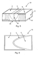
Figure 5 shows asemiconductor device 10 in accordance with a further embodiment of this invention. In this example, abarrier 30 is provided in thesubstrate 12. Thebarrier 30 can act to at least partially block direct current flow between thefirst contact 4 and thesecond contact 6, thereby increasing the proportion of the overall current that flows between thefirst contact 4 and thesecond contact 6 via themetal layer 20 on thebackside 18. This is because the route taken by any current passing directly from thefirst contact 4 to thesecond contact 6 through the bulk would need to travel beneath thebarrier 30, increasing the path length of such a route and thus presenting a greater resistance to such current a current compared to the current path that includes themetal layer 20. - The shape of the
barrier 30 may, in some examples, be chosen to conform to the shape and layout of the contacts on the major surface. - In this example, the
barrier 30 comprises a trench that extends from themajor surface 2 of thesubstrate 12 at least partially through thesubstrate 12. The trench may be formed by etching. The trench may be filled with a dielectric material. Because more of the current is forced to flow via themetal layer 20, the current distribution within the bulk of thesubstrate 12 can be further improved in comparison to, for example, the examples described above in relation toFigures 2 to 4 . - It will be appreciated that the use of a
barrier 30 such as that shown inFigure 5 can be combined with the provision of features of the other embodiments described herein (for instance the third contact as described above in relation toFigure 3 and/or a patterned metal layer as described in relation toFigure 4 ). -
Figure 6 shows asemiconductor device 10 in accordance with a further embodiment of this invention. The view inFigure 6 is from above thesubstrate 12, looking down at themajor surface 2. As can be seen inFigure 6 , in this example thedevice 10 includes afirst contact 4 and asecond contact 6 on themajor surface 2. The layout of the contacts in this example is chosen such that thefirst contact 4 at least partially surrounds thesecond contact 6. For instance, inFigure 6 , thesecond contact 6 is received within a generally U-shaped recess in thefirst contact 4. An arrangement of this kind has been found to further improve the current handling capability of thedevice 10. It will be appreciated that the shaping of the contacts in this way can be combined with other features of the invention such as those described above in relation toFigures 2 to 5 and also in relation to the further examples provided below. - Although embodiments of this invention can produce a generally even current distribution within the device, because the current is required to pass twice through the bulk of substrate the overall resistance of the current path in the device may still be improved. The examples of the invention described below may address this problem using a number of further features.
-
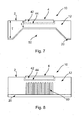
Figure 7 shows asemiconductor device 10 in accordance with another embodiment of this invention.Figure 7 shows only a portion of thedevice 10, namely the portion that includes one of the contacts (in the embodiment ofFigure 7 , this is the contact 4) on themajor surface 2 as described above. - In some embodiments, the substrate may include a
pn junction 44 formed between the bulk of thesubstrate 12 and a portion ofsemiconductor material 42 that is provided beneath one of the contacts (again, in the example shown inFigure 7 , this is the contact 4). For clarity, the possible presence of such aportion 42 andpn junction 44 was not illustrated in the previously described Figures. Note that the thinner portions (e.g. grooves) described below may be provided in examples that do not include aportion 42 or pn junction of the kind shown inFigure 7 . - In order to reduce the resistance of the path from the
first contact 4 to themetal layer 20 provided on the backside of thesubstrate 12, in this embodiment thesubstrate 12 is thinner in the vicinity of thecontact 4 than it is elsewhere. The thickness t of thesubstrate 12 in the vicinity of thecontact 4 is, for example, smaller than the thickness T of thesubstrate 12 away from the contact 4 (for instance, outside an active region of the device 10). Accordingly, because thesubstrate 12 is thinner in the vicinity of thecontact 4, the resistive path between thecontact 4 and themetal layer 20 is reduced. The thinner part of thesubstrate 12 in this example is formed by agroove 50 in the backside surface of thesubstrate 12. Thegroove 50 may be shaped similarly to the shape of thecontact 4 on the opposite surface (when viewed from above the major surface 2) and may be formed using an etching process during wafer processing. - It is envisaged that in some embodiments, the
substrate 12 may be thinner in the vicinity of more than one contact. For instance, an area of thesubstrate 12 including more than one contact may be thinned. For example a relatively wide groove may be provided that encompasses an area including a plurality of contacts. Alternatively, thesubstrate 12 may be locally thinned in the vicinity of each of a plurality of respective contacts (e.g. a respective groove may be provided for each contact). - It is further envisaged that the provision of a thinner part of the
substrate 12 as explained above in relation toFigure 7 may be implemented in combination with the features of any of the other embodiments described herein. -
Figure 8 shows asemiconductor device 10 in accordance with a further embodiment of this invention. In common withFigure 7, Figure 8 shows only a part of the device, namely the part of the device that includes thefirst contact 4. In this example, thedevice 10 includes an electrically conductive portion that extends from themetal layer 20 on thebackside 18, partially through thesubstrate 12 toward thecontact 4. It is envisaged that in other examples, electrically conductive portions of this kind may be provided for other contacts of the device, such as thesecond contact 6. In one example, both thecontact 4 and thecontact 6 are provided with electrically conductive portions of this kind. In a further example, the electrically conductive portion(s) may be provided not just for any given contact location but also in other regions of the substrate. For instance, it is envisaged that the trenches and/or vias described below may be provided over a large area of the substrate, or even over the entire substrate. The provision of the electrically conductive portion can lower the overall resistance of the path between thefirst contact 4 and themetal layer 20. - In the present embodiment, the electrically conductive portion comprises one or more vias that are filled with an electrically conductive material such as a metal. In another example, the electrically conductive portion may comprise one or more trenches, also containing metal. It is envisaged that a combination of vias and trenches may be used. The metal that is used in the vias or trenches may be the same metal that is used to form the
metal layer 20 and/or the metals of thetop contacts -
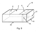
Figure 9 shows a semiconductor device according to another embodiment of this invention. In this example, one of the contacts (inFigure 9 this is shown to be thesecond contact 6, but it is envisaged that it may be one of the other contacts of the device such as the contact 4) is electrically connected to themetal layer 20 on thebackside 18 of thesubstrate 12 by an electricallyconductive portion 70 that extends through the substrate from thecontact 6 to themetal layer 20. The provision of the electrically conductive portion can reduce the overall resistance of the current path between thefirst contact 4 and thesecond contact 6 via themetal layer 20. In the present example, the electrically conductive portion includes one ormore vias 70 that may contain a metal. It is envisaged that trenches may be used instead of or as well as vias to form the electrically conductive portion. The trenches and/orvias 70 may be filed with a metal that is the same metal as that used to form themetal layer 20 on thebackside 18 of thesubstrate 12 and/or the metals of the top contacts. - It is envisaged that the electrically conductive portions described in relation to
Figures 8 and9 can be combined with any of the features of the invention described in relation toFigures 2 to 7 . - To manufacture a device in accordance with an embodiment of this invention, a semiconductor wafer can first be provided with a plurality of contacts on a major surface thereof. In a next step, an electrically floating metal layer can be deposited on a backside of the wafer to form an ohmic contact thereto. The wafer can then be diced. Each of the dice from the wafer can form a semiconductor device of the kind described herein. Features of the invention such as the grooves discussed in relation to
Figure 7 and the electrically conductive portion discussed in relation toFigures 8 and9 , as well as the layout of the contacts discussed in relation toFigure 6 and the provision of a patternedmetal layer 20 or a barrier described in relation toFigures 4 and5 , respectively can be manufactured at wafer level and repeated in each intended die, before the dies are cut individually from the wafer. - Accordingly, there has been described a semiconductor device and a method of making the same. The device includes a semiconductor substrate provided in a chip-scale package (CSP). The device also includes a plurality of contacts provided on a major surface of the substrate. The device further includes an electrically floating metal layer forming an ohmic contact on a backside of the semiconductor substrate. The device is operable to conduct a current that passes through the substrate from a first of said plurality of contacts to a second of said plurality of contacts via the metal layer on the backside.
- Although particular embodiments of the invention have been described, it will be appreciated that many modifications/additions and/or substitutions may be made within the scope of the claimed invention.
Claims (15)
- A semiconductor device comprising:a semiconductor substrate provided in a chip-scale package (CSP);a plurality of contacts provided on a major surface of the substrate, andan electrically floating metal layer forming an ohmic contact on a backside of the semiconductor substrate,
wherein the device is operable to conduct a current that passes through the substrate from a first of said plurality of contacts to a second of said plurality of contacts via the metal layer on the backside. - The semiconductor device of claim 1, wherein either the first contact or the second contact is electrically connected to the electrically floating metal layer by an electrically conductive portion extending through the substrate from the first or second contact to the electrically floating metal layer.
- The semiconductor device of claim 2, wherein the electrically conductive portion comprises one or more vias and/or trenches containing metal.
- The semiconductor device of any preceding claim, wherein the substrate is thinner in the vicinity of at least one of the contacts than it is outside an active region of the device, for reducing electrical resistance of the path between the contact and the metal layer on the backside.
- The semiconductor device of claim 4, wherein the thinner part of the substrate comprises one or more grooves located on the backside of the substrate.
- The semiconductor device of any preceding claim comprising an electrically conductive portion extending from the metal layer on the backside, partially through the substrate toward one or more of said plurality of contacts.
- The semiconductor device of claim 6, wherein the electrically conductive portion extending from the metal layer on the backside comprises one or more vias and/or trenches containing metal.
- The semiconductor device of any preceding claim, wherein the metal layer contacts only those parts of the backside of the substrate that are located substantially opposite the first contact and the second contact on the major surface.
- The semiconductor device of any preceding claim, further comprising a barrier located in the substrate between the first contact and the second contact, for at least partially blocking direct current flow between the first contact and the second contact.
- The semiconductor device of claim 9, wherein the barrier comprises a trench containing a dielectric, wherein the trench extends from the major surface of the substrate at least partially through the substrate.
- The semiconductor device of any preceding claim, wherein at least one of said plurality of contacts at least partially surrounds another of said plurality of contacts on said major surface.
- The semiconductor device of any preceding claim, wherein the device is a transient voltage suppression (TVS) diode.
- The semiconductor device of any of claims 1 to 11, wherein:said plurality of contacts includes a third contact; andthe device comprises a bipolar transistor in which the first contact is an emitter contact, the second contact is a collector contact, and the third contact is a base contact; orthe device comprises a MOS transistor in which the first contact is a source contact, the second contact is a drain contact, and the third contact is a gate contact.
- The semiconductor device of any preceding claim mounted on a surface of a carrier, wherein the electrically floating metal layer is not connected any external pin of the device.
- A method comprising:providing a semiconductor wafer;providing a plurality of contacts on a major surface of the wafer;providing an electrically floating metal layer forming an ohmic contact on a backside of the wafer, anddicing the wafer for making a plurality of semiconductor devices according to any preceding claim.
Priority Applications (3)
| Application Number | Priority Date | Filing Date | Title |
|---|---|---|---|
| EP15152673.8A EP3051592A1 (en) | 2015-01-27 | 2015-01-27 | Semiconductor device |
| US14/988,443 US10643941B2 (en) | 2015-01-27 | 2016-01-05 | Semiconductor device |
| CN201610052223.1A CN105826366B (en) | 2015-01-27 | 2016-01-26 | Semiconductor device |
Applications Claiming Priority (1)
| Application Number | Priority Date | Filing Date | Title |
|---|---|---|---|
| EP15152673.8A EP3051592A1 (en) | 2015-01-27 | 2015-01-27 | Semiconductor device |
Publications (1)
| Publication Number | Publication Date |
|---|---|
| EP3051592A1 true EP3051592A1 (en) | 2016-08-03 |
Family
ID=52394195
Family Applications (1)
| Application Number | Title | Priority Date | Filing Date |
|---|---|---|---|
| EP15152673.8A Withdrawn EP3051592A1 (en) | 2015-01-27 | 2015-01-27 | Semiconductor device |
Country Status (3)
| Country | Link |
|---|---|
| US (1) | US10643941B2 (en) |
| EP (1) | EP3051592A1 (en) |
| CN (1) | CN105826366B (en) |
Cited By (4)
| Publication number | Priority date | Publication date | Assignee | Title |
|---|---|---|---|---|
| US11393699B2 (en) | 2019-12-24 | 2022-07-19 | Vishay General Semiconductor, Llc | Packaging process for plating with selective molding |
| US11450534B2 (en) | 2019-12-24 | 2022-09-20 | Vishay General Semiconductor, Llc | Packaging process for side-wall plating with a conductive film |
| US12211704B2 (en) | 2019-03-08 | 2025-01-28 | Siliconix Incorporated | Semiconductor package having side wall plating |
| US12224232B2 (en) | 2019-03-08 | 2025-02-11 | Siliconix Incorporated | Semiconductor package having side wall plating |
Families Citing this family (4)
| Publication number | Priority date | Publication date | Assignee | Title |
|---|---|---|---|---|
| CN106783949A (en) * | 2016-12-19 | 2017-05-31 | 东莞市阿甘半导体有限公司 | Unidirectional TVS structures and its manufacture method |
| US10510663B2 (en) * | 2017-03-30 | 2019-12-17 | Globalfoundries Inc. | Transistor structures having electrically floating metal layer between active metal lines |
| JP7294594B2 (en) | 2019-06-03 | 2023-06-20 | リテルヒューズ・セミコンダクター・(ウーシー)・カンパニー・リミテッド | Integrated multi-device chips and packages |
| CN115020500B (en) * | 2022-07-21 | 2025-11-28 | 西安电子科技大学 | Gallium oxide Schottky diode capable of reducing on-resistance and preparation method thereof |
Citations (8)
| Publication number | Priority date | Publication date | Assignee | Title |
|---|---|---|---|---|
| US20030057503A1 (en) * | 2001-09-26 | 2003-03-27 | Kabushiki Kaisha Toshiba | Semiconductor device |
| EP1793426A2 (en) * | 2005-11-30 | 2007-06-06 | Sharp Kabushiki Kaisha | Semiconductor device having a via hole and its manufacturing method |
| JP2007142272A (en) * | 2005-11-21 | 2007-06-07 | Sanyo Electric Co Ltd | Semiconductor device |
| EP1848031A1 (en) * | 2006-04-21 | 2007-10-24 | Sanyo Electric Co., Ltd. | Semiconductor device and method of manufacturing the same |
| JP2007317839A (en) * | 2006-05-25 | 2007-12-06 | Sanyo Electric Co Ltd | Semiconductor device and manufacturing method thereof |
| JP2010206235A (en) * | 2007-11-09 | 2010-09-16 | Denso Corp | Semiconductor device |
| US20140167204A1 (en) * | 2012-12-13 | 2014-06-19 | Diodes Incorporated | Semiconductor diode assembly |
| EP2802013A1 (en) * | 2009-10-30 | 2014-11-12 | Vishay-Siliconix | Semiconductor device |
Family Cites Families (13)
| Publication number | Priority date | Publication date | Assignee | Title |
|---|---|---|---|---|
| US6515330B1 (en) * | 2002-01-02 | 2003-02-04 | Apd Semiconductor, Inc. | Power device having vertical current path with enhanced pinch-off for current limiting |
| US6858471B1 (en) * | 2002-09-20 | 2005-02-22 | Vishay-Siliconix | Semiconductor substrate with trenches for reducing substrate resistance |
| US6756687B1 (en) * | 2003-03-05 | 2004-06-29 | Altera Corporation | Interfacial strengthening for electroless nickel immersion gold substrates |
| US7485941B2 (en) * | 2004-12-15 | 2009-02-03 | Tower Semiconductor Ltd. | Cobalt silicide schottky diode on isolated well |
| JP5261636B2 (en) * | 2006-10-27 | 2013-08-14 | セミコンダクター・コンポーネンツ・インダストリーズ・リミテッド・ライアビリティ・カンパニー | Semiconductor device |
| US20090079072A1 (en) * | 2007-09-21 | 2009-03-26 | Casio Computer Co., Ltd. | Semiconductor device having low dielectric insulating film and manufacturing method of the same |
| US9169554B2 (en) * | 2008-05-30 | 2015-10-27 | Alta Devices, Inc. | Wafer carrier track |
| JP2010026235A (en) | 2008-07-18 | 2010-02-04 | Panasonic Electric Works Co Ltd | Camera angle controller |
| US8058732B2 (en) * | 2008-11-20 | 2011-11-15 | Fairchild Semiconductor Corporation | Semiconductor die structures for wafer-level chipscale packaging of power devices, packages and systems for using the same, and methods of making the same |
| US7960800B2 (en) * | 2008-12-12 | 2011-06-14 | Fairchild Semiconductor Corporation | Semiconductor dice with backside trenches filled with elastic material for improved attachment, packages using the same, and methods of making the same |
| RU2605089C2 (en) | 2011-07-15 | 2016-12-20 | Акцо Нобель Коатингс Интернэшнл Б.В. | Adhesive system |
| US9224669B2 (en) * | 2011-08-09 | 2015-12-29 | Alpha And Omega Semiconductor Incorporated | Method and structure for wafer level packaging with large contact area |
| US10090672B2 (en) * | 2015-12-02 | 2018-10-02 | Hamilton Sundstrand Corporation | Shared transient voltage suppressor having built-in-test capability for solid state power controllers |
-
2015
- 2015-01-27 EP EP15152673.8A patent/EP3051592A1/en not_active Withdrawn
-
2016
- 2016-01-05 US US14/988,443 patent/US10643941B2/en active Active
- 2016-01-26 CN CN201610052223.1A patent/CN105826366B/en active Active
Patent Citations (8)
| Publication number | Priority date | Publication date | Assignee | Title |
|---|---|---|---|---|
| US20030057503A1 (en) * | 2001-09-26 | 2003-03-27 | Kabushiki Kaisha Toshiba | Semiconductor device |
| JP2007142272A (en) * | 2005-11-21 | 2007-06-07 | Sanyo Electric Co Ltd | Semiconductor device |
| EP1793426A2 (en) * | 2005-11-30 | 2007-06-06 | Sharp Kabushiki Kaisha | Semiconductor device having a via hole and its manufacturing method |
| EP1848031A1 (en) * | 2006-04-21 | 2007-10-24 | Sanyo Electric Co., Ltd. | Semiconductor device and method of manufacturing the same |
| JP2007317839A (en) * | 2006-05-25 | 2007-12-06 | Sanyo Electric Co Ltd | Semiconductor device and manufacturing method thereof |
| JP2010206235A (en) * | 2007-11-09 | 2010-09-16 | Denso Corp | Semiconductor device |
| EP2802013A1 (en) * | 2009-10-30 | 2014-11-12 | Vishay-Siliconix | Semiconductor device |
| US20140167204A1 (en) * | 2012-12-13 | 2014-06-19 | Diodes Incorporated | Semiconductor diode assembly |
Cited By (6)
| Publication number | Priority date | Publication date | Assignee | Title |
|---|---|---|---|---|
| US12211704B2 (en) | 2019-03-08 | 2025-01-28 | Siliconix Incorporated | Semiconductor package having side wall plating |
| US12224232B2 (en) | 2019-03-08 | 2025-02-11 | Siliconix Incorporated | Semiconductor package having side wall plating |
| US11393699B2 (en) | 2019-12-24 | 2022-07-19 | Vishay General Semiconductor, Llc | Packaging process for plating with selective molding |
| US11450534B2 (en) | 2019-12-24 | 2022-09-20 | Vishay General Semiconductor, Llc | Packaging process for side-wall plating with a conductive film |
| US11764075B2 (en) | 2019-12-24 | 2023-09-19 | Vishay General Semiconductor, Llc | Package assembly for plating with selective molding |
| US11876003B2 (en) | 2019-12-24 | 2024-01-16 | Vishay General Semiconductor, Llc | Semiconductor package and packaging process for side-wall plating with a conductive film |
Also Published As
| Publication number | Publication date |
|---|---|
| US20160218058A1 (en) | 2016-07-28 |
| CN105826366A (en) | 2016-08-03 |
| US10643941B2 (en) | 2020-05-05 |
| CN105826366B (en) | 2019-03-22 |
Similar Documents
| Publication | Publication Date | Title |
|---|---|---|
| US10643941B2 (en) | Semiconductor device | |
| US20240339421A1 (en) | Electronic component and semiconductor device | |
| US10163772B2 (en) | Stacked semiconductor device structure and method | |
| US9224827B2 (en) | High voltage resistor | |
| US9324645B2 (en) | Method and system for co-packaging vertical gallium nitride power devices | |
| EP2779246A2 (en) | Method of forming a high electron mobility semiconductor device and structure therefor | |
| US12027579B2 (en) | Semiconductor device having a carrier trapping region including crystal defects | |
| US9966277B2 (en) | Arrangement and method for manufacturing the same | |
| US9324809B2 (en) | Method and system for interleaved boost converter with co-packaged gallium nitride power devices | |
| US9917159B2 (en) | Semiconductor device comprising planar gate and trench field electrode structure | |
| US8937317B2 (en) | Method and system for co-packaging gallium nitride electronics | |
| US10411126B2 (en) | Semiconductor device having a first through contact structure in ohmic contact with the gate electrode | |
| KR20160110011A (en) | Semiconductor apparatus and semiconductor package | |
| US10340264B2 (en) | Semiconductor device comprising a clamping structure | |
| US20250022710A1 (en) | Semiconductor device and method of manufacturing semiconductor device | |
| US9287377B2 (en) | Semiconductor device and manufacturing method | |
| CN111902937A (en) | Semiconductor device and method for manufacturing the same | |
| US20070272980A1 (en) | Semiconductor device with vertical current flow and low substrate resistance and manufacturing process thereof | |
| CN109817726B (en) | Asymmetric transient voltage suppressor device and method of forming the same | |
| KR20220008330A (en) | Power Semiconductor Device With Reflowed Intermetallic Dielectric Layers | |
| US20260053057A1 (en) | Encapsulation delamination prevention structures at die edge | |
| TWI823771B (en) | Vertical semiconductor power device and method for manufacturing the same | |
| US20240274697A1 (en) | Semiconductor device and method of manufacturing the same | |
| US20240030344A1 (en) | Semiconductor device | |
| US20260083012A1 (en) | Semiconductor device and method of manufacturing the same |
Legal Events
| Date | Code | Title | Description |
|---|---|---|---|
| PUAI | Public reference made under article 153(3) epc to a published international application that has entered the european phase |
Free format text: ORIGINAL CODE: 0009012 |
|
| AK | Designated contracting states |
Kind code of ref document: A1 Designated state(s): AL AT BE BG CH CY CZ DE DK EE ES FI FR GB GR HR HU IE IS IT LI LT LU LV MC MK MT NL NO PL PT RO RS SE SI SK SM TR |
|
| AX | Request for extension of the european patent |
Extension state: BA ME |
|
| RAP1 | Party data changed (applicant data changed or rights of an application transferred) |
Owner name: NEXPERIA B.V. |
|
| 17P | Request for examination filed |
Effective date: 20170203 |
|
| RBV | Designated contracting states (corrected) |
Designated state(s): AL AT BE BG CH CY CZ DE DK EE ES FI FR GB GR HR HU IE IS IT LI LT LU LV MC MK MT NL NO PL PT RO RS SE SI SK SM TR |
|
| RAP1 | Party data changed (applicant data changed or rights of an application transferred) |
Owner name: NEXPERIA B.V. |
|
| 17Q | First examination report despatched |
Effective date: 20180927 |
|
| STAA | Information on the status of an ep patent application or granted ep patent |
Free format text: STATUS: THE APPLICATION IS DEEMED TO BE WITHDRAWN |
|
| 18D | Application deemed to be withdrawn |
Effective date: 20190409 |