EP3050199B1 - Mehrstufenumrichtervorrichtung und verfahren mit vorspannungsschaltung mit geklemmtem knoten - Google Patents
Mehrstufenumrichtervorrichtung und verfahren mit vorspannungsschaltung mit geklemmtem knoten Download PDFInfo
- Publication number
- EP3050199B1 EP3050199B1 EP14777469.9A EP14777469A EP3050199B1 EP 3050199 B1 EP3050199 B1 EP 3050199B1 EP 14777469 A EP14777469 A EP 14777469A EP 3050199 B1 EP3050199 B1 EP 3050199B1
- Authority
- EP
- European Patent Office
- Prior art keywords
- node
- coupled
- clamped
- transistor
- transistors
- Prior art date
- Legal status (The legal status is an assumption and is not a legal conclusion. Google has not performed a legal analysis and makes no representation as to the accuracy of the status listed.)
- Active
Links
Images


Classifications
-
- H—ELECTRICITY
- H02—GENERATION; CONVERSION OR DISTRIBUTION OF ELECTRIC POWER
- H02M—APPARATUS FOR CONVERSION BETWEEN AC AND AC, BETWEEN AC AND DC, OR BETWEEN DC AND DC, AND FOR USE WITH MAINS OR SIMILAR POWER SUPPLY SYSTEMS; CONVERSION OF DC OR AC INPUT POWER INTO SURGE OUTPUT POWER; CONTROL OR REGULATION THEREOF
- H02M7/00—Conversion of AC power input into DC power output; Conversion of DC power input into AC power output
- H02M7/66—Conversion of AC power input into DC power output; Conversion of DC power input into AC power output with possibility of reversal
- H02M7/68—Conversion of AC power input into DC power output; Conversion of DC power input into AC power output with possibility of reversal by static converters
- H02M7/72—Conversion of AC power input into DC power output; Conversion of DC power input into AC power output with possibility of reversal by static converters using discharge tubes with control electrode or semiconductor devices with control electrode
- H02M7/79—Conversion of AC power input into DC power output; Conversion of DC power input into AC power output with possibility of reversal by static converters using discharge tubes with control electrode or semiconductor devices with control electrode using devices of a triode or transistor type requiring continuous application of a control signal
- H02M7/797—Conversion of AC power input into DC power output; Conversion of DC power input into AC power output with possibility of reversal by static converters using discharge tubes with control electrode or semiconductor devices with control electrode using devices of a triode or transistor type requiring continuous application of a control signal using semiconductor devices only
-
- H—ELECTRICITY
- H02—GENERATION; CONVERSION OR DISTRIBUTION OF ELECTRIC POWER
- H02M—APPARATUS FOR CONVERSION BETWEEN AC AND AC, BETWEEN AC AND DC, OR BETWEEN DC AND DC, AND FOR USE WITH MAINS OR SIMILAR POWER SUPPLY SYSTEMS; CONVERSION OF DC OR AC INPUT POWER INTO SURGE OUTPUT POWER; CONTROL OR REGULATION THEREOF
- H02M1/00—Details of apparatus for conversion
- H02M1/32—Means for protecting converters other than automatic disconnection
-
- H—ELECTRICITY
- H02—GENERATION; CONVERSION OR DISTRIBUTION OF ELECTRIC POWER
- H02M—APPARATUS FOR CONVERSION BETWEEN AC AND AC, BETWEEN AC AND DC, OR BETWEEN DC AND DC, AND FOR USE WITH MAINS OR SIMILAR POWER SUPPLY SYSTEMS; CONVERSION OF DC OR AC INPUT POWER INTO SURGE OUTPUT POWER; CONTROL OR REGULATION THEREOF
- H02M7/00—Conversion of AC power input into DC power output; Conversion of DC power input into AC power output
- H02M7/42—Conversion of DC power input into AC power output without possibility of reversal
- H02M7/44—Conversion of DC power input into AC power output without possibility of reversal by static converters
- H02M7/48—Conversion of DC power input into AC power output without possibility of reversal by static converters using discharge tubes with control electrode or semiconductor devices with control electrode
- H02M7/483—Converters with outputs that each can have more than two voltages levels
- H02M7/487—Neutral point clamped inverters
-
- H—ELECTRICITY
- H02—GENERATION; CONVERSION OR DISTRIBUTION OF ELECTRIC POWER
- H02M—APPARATUS FOR CONVERSION BETWEEN AC AND AC, BETWEEN AC AND DC, OR BETWEEN DC AND DC, AND FOR USE WITH MAINS OR SIMILAR POWER SUPPLY SYSTEMS; CONVERSION OF DC OR AC INPUT POWER INTO SURGE OUTPUT POWER; CONTROL OR REGULATION THEREOF
- H02M7/00—Conversion of AC power input into DC power output; Conversion of DC power input into AC power output
- H02M7/02—Conversion of AC power input into DC power output without possibility of reversal
- H02M7/04—Conversion of AC power input into DC power output without possibility of reversal by static converters
- H02M7/12—Conversion of AC power input into DC power output without possibility of reversal by static converters using discharge tubes with control electrode or semiconductor devices with control electrode
- H02M7/21—Conversion of AC power input into DC power output without possibility of reversal by static converters using discharge tubes with control electrode or semiconductor devices with control electrode using devices of a triode or transistor type requiring continuous application of a control signal
- H02M7/217—Conversion of AC power input into DC power output without possibility of reversal by static converters using discharge tubes with control electrode or semiconductor devices with control electrode using devices of a triode or transistor type requiring continuous application of a control signal using semiconductor devices only
Definitions
- the inventive subject matter relates to power conversion circuits and methods and, more particularly, to inverter apparatus and methods.
- Rectifier and inverter circuits are used in uninterruptible power supply (UPS) systems, motor drives and other power apparatus.
- Some inverters and rectifiers have a multilevel architecture that uses multiple commutation states.
- Various multilevel inverter and rectifier circuits are described, for example, in U.S. Patent No. 5,361,196 to Tamamachi et al. , U.S. Patent No. 6,031,738 to Lipo et al. , U.S. Patent No. 6,795,323 to Tanaka et al. , U.S. Patent No. 6,838,925 to Nielsen , U.S. Patent No. 7,145,268 to Edwards et al. and U.S. Patent No.
- a multi-level converter as set forth in claim 1 and a method of operating a multi-level converter as set forth in claim 9 are provided. Further embodiments are inter alia disclosed in the dependent claims.
- Embodiments of the inventive subject matter provide a multi-level converter including first and second DC buses, a plurality of transistors coupled in series between the first and second DC buses and a clamp circuit configured to clamp a node joining a first transistor and a second transistor of the plurality of transistors.
- An AC node is coupled to the plurality of transistors, wherein the second transistor is coupled between the clamped node and the AC node and the first transistor is coupled between the second transistor and the first DC bus.
- a bias circuit comprising a resistor couples the clamped node to the second DC bus.
- the converter may be configured to operate as a rectifier and the second transistor may be coupled between the clamped node and a phase input. In further embodiments, the converter may be configured to operate as an inverter and the second transistor may be coupled between the clamped node and a phase output.
- the bias circuit may be configured to couple the clamped node to the first DC bus and the first and second transistors may be coupled between the second DC bus and an AC node.
- the bias circuit may include a resistor coupling the clamped node to the first DC bus.
- the bias circuit may be further configured to discharge a capacitance coupled to the first DC bus using the clamp circuit.
- the converter may further include third and fourth transistors coupled in series between the second DC bus and the AC node, a second diode coupled between the neutral node and a second neutral clampe
- Still further embodiments provide methods of operating a multi-level converter comprising a plurality of transistors coupled in series between the first and second DC buses, and a clamp circuit configured to clamp a node joining a first transistor and a second transistor of the plurality of transistors to a neutral node of the multi-level converter, wherein the second transistor is coupled between the clamped node and an AC node and the first transistor is coupled between the second transistor and the first DC bus, the method comprising: coupling the clamped node to the second DC bus via a resistor to bias the clamped node to a predetermined voltage and thereby limit a voltage developed across the second transistor.
- FIG. 1 illustrates a multi-level converter 100 according to an unclaimed example useful for understanding the invention
- the converter 100 may be utilized as an inverter and/or rectifier, and includes a plurality of transistors, here shown as first, second, third and fourth insulated gate bipolar transistors (IGBTs) Q1, Q2, Q3, Q4.
- the first and second transistors Q1, Q2 are coupled between a first DC bus 115a and an AC node 114 and the third and fourth transistors Q3, Q4 are coupled between a second DC bus 115b and the AC node 114.
- the AC node 114 may be coupled to an external source and/or load via an inductor L.
- the transistors Q1, Q2, Q3, Q4 may be controlled by a control circuit 118.
- Anti-parallel diodes paired with the transistors Q1, Q2, Q2, Q4 may be integrated with the transistors or may be separate components.
- Nodes 112a, 112b between first and second transistors Q1, Q2 and third and fourth transistors Q3, Q4, respectively, are neutral clamped using respective diodes D1, D2 coupled between the nodes 112a, 112b and a neutral node N.
- the neutral clamping supports multilevel operation.
- the converter 100 includes bias circuits 116a, 116b coupled to the neutral clamped nodes 112a, 112b.
- the bias circuits 116a, 116b are configured to bias the neutral clamped nodes 112a, 112b to a predetermined voltage when the first and fourth transistors Q1, Q4 are off.
- the bias circuits 116a, 116b may serve to limit voltage developed across the inner transistors Q2, Q3 under certain conditions.
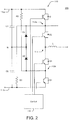
- FIG. 2 illustrates a multilevel converter 200 according to embodiments of the invention, wherein clamped node biasing is provided by resistors coupled to DC buses.
- the converter 200 includes first and second DC buses 115a, 115b, first, second, third and fourth transistors Q1, Q2, Q3, Q4, neutral clamping diodes D1, D2, inductor L, AC node 114 and first and second neutral clamping nodes 112a, 112b as described above with reference to FIG. 1 .
- a first bias resistor R1 is coupled between the first neutral clamped node 112a and the second DC bus 115b.
- a second bias resistor R2 is coupled between the second neutral clamped node 112b and the first DC bus 115a.
- the bias provided by the resistors R1, R2 can prevent damaging voltage levels from developing across the inner second and third transistors Q2, Q3 if, for example, a voltage surge occurs in a line coupled to the AC node 114 while the converter 200 is in an inactive state with all of the transistors Q1, Q2, Q3, Q4 off.
- the resistors R1, R2 may have resistance values sufficient to provide bias to protect the inner second and third transistors Q2, Q3, without supporting unduly large currents between the buses 115a, 115b and the neutral N.
- the first and second bias resistors R1, R2 may also support discharging (bleeding) of capacitors C1, C2 coupled to the first and second DC buses 115a, 115b via the neutral clamping diodes D1, D2 to de-energize the buses 115a, 115b for maintenance and other purposes.
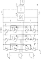
- FIG. 3 illustrates a UPS 300 including a rectifier 310, which has phase inputs 311a, 311b, 311c configured to be coupled to an AC source, such as a utility or generator.
- An output of the rectifier 310 is coupled to an inverter circuit 330 by first and second DC buses 315a, 315b.
- the inverter circuit has phase outputs 331a, 331b, 331c configured to be coupled to a load.
- an auxiliary power source 420 such as a battery or battery converter configured to be coupled to a battery, may also be coupled to the first and second DC buses 315a, 315b.
- Storage capacitors C1, C2 are coupled between respective ones of the first and second DC buses 315a, 315b and a neutral N.
- the rectifier 310 may be a multi-level rectifier having phase inputs 311a, 311b, 311c and including input inductors La, Lb, Lc, upper transistors Q1a, Q2a, Q1b, Q2b, Q1c, Q2c coupled between the first DC bus 315a and the neutral N, and lower transistors Q3a, Q4a, Q3b, Q4b, Q3c, Q4c coupled between the second DC bus 315b and the neutral N.
- Diodes D1a, D2a, D1b, D2b, D1c, D2c provide neutral clamping of respective nodes 312 between respective ones of the upper and lower transistor pairs.
- Resistors R1a, R2a, R1b, R2b, R1c, R2c bias the neutral clamped nodes 312 and provide current paths for discharging the first and second DC buses 315a, 315b.
- the UPS 300 may also include control circuitry (not shown for clarity of illustration) for driving the transistors Q1a, Q2a, Q1b, Q2b, Q1c, Q2c, Q3a, Q4a, Q3b, Q4b, Q3c, Q4c, as well as additional circuitry, such as bypass circuitry.
- FIG. 4 illustrates a UPS 400 including a rectifier 410 having phase inputs 411a, 411b, 411c configured to be coupled to an AC source, such as a utility or generator.
- An output of the rectifier 410 is coupled to an inverter circuit 430 by first and second DC buses 415a, 415b.
- the inverter circuit has phase outputs 431a, 431b, 431c configured to be coupled to a load.
- an auxiliary power source 420 may also be coupled to the first and second DC buses 415a, 415b.
- Storage capacitors C1, C2 are coupled between respective ones of the first and second DC buses 415a, 415b to a neutral N.
- the inverter 430 may be a multi-level inverter including output inductors La, Lb, Lc, upper transistors Q1a, Q2a, Q1b, Q2b, Q1c, Q2c coupled between the first DC bus 415a and the neutral N, and lower transistors Q3a, Q4a, Q3b, Q4b, Q3c, Q4c coupled between the second DC bus 415b and the neutral N.
- Diodes D1a, D2a, D1b, D2b, D1c, D2c provide neutral clamping of respective nodes 412 between respective ones of the upper and lower transistor pairs.
- Resistors R1a, R2a, R1b, R2b, R1c, R2c bias the neutral clamped nodes 412 and provide discharge paths for the first and second DC buses 415a, 415b.
- the UPS 400 may also include control circuitry for driving the transistors Q1a, Q2a, Q1b, Q2b, Q1c, Q2c, Q3a, Q4a, Q3b, Q4b, Q3c, Q4c (not shown for clarity of illustration), along with other circuitry, such as bypass circuitry.
- converters according to some embodiments of the inventive subject matter may be used in any of a number of different applications, such as rectifiers, inverters, motor drives and the like. Further embodiments may use bias circuits other than the resistor connections described above with reference to FIGs. 2-4 , such as bias circuits that use other passive networks and/or active devices to provide similar biasing. It will further appreciated that, although the illustrated example embodiments include three-level converters with neutral clamped nodes, some embodiments of the inventive subject matter may provide other types of multi-level converters, such as converters with more than four transistors and/or more than three states, having nodes that are clamped in other ways and biased using bias circuitry similar to that described above.
Landscapes
- Engineering & Computer Science (AREA)
- Power Engineering (AREA)
- Inverter Devices (AREA)
- Rectifiers (AREA)
Claims (14)
- Ein Multilevelkonverter (100, 200), der Folgendes aufweist:erste und zweite Gleichstromsammelleitungen bzw. DC Busse (115a, 115b, 315a, 315b, 415a, 415b);eine Vielzahl von Transistoren (Q1a, Q2a, Q1b, Q2b, Q1c, Q2c, Q3a, Q4a, Q3b, Q4b, Q3c, Q4c) in Serie geschaltet zwischen den ersten und zweiten DC-Bussen (115a, 115b, 315a, 315b, 415a, 415b);eine Klemmschaltung, konfiguriert zum Klemmen eines Knotens (112a), der einen ersten Transistor (Q1a, Q1b, Q1c) und einen zweiten Transistor (Q2a, Q2b, Q2c) der Vielzahl von Transistoren (Q1a, Q2a, Q1b, Q2b, Q1c, Q2c, Q3a, Q4a, Q3b, Q4b, Q3c, Q4c) verbindet, und zwar mit einem neutralen Knoten (N) des Multilevelkonverters (100, 200);einen AC-Knoten (114), verbunden mit der Vielzahl von Transistoren (Q1a, Q2a, Q1b, Q2b, Q1c, Q2c, Q3a, Q4a, Q3b, Q4b, Q3c, Q4c), wobei der zweite Transistor (Q2a, Q2b, Q2c) verbunden ist zwischen dem geklemmten Knoten (112a, 312, 412) und dem AC-Knoten (114) und der erste Transistor (Q1a, Q1b, Q1c) verbunden ist zwischen dem zweiten Transistor (Q2a, Q2b, Q2c) und dem ersten DC-Bus (115a, 315a, 415a); undeine Vorspannschaltung (116a); dadurch gekennzeichnet, dass die Vorspannschaltung einen Widerstand (R1a, R1b, R1c) aufweist, der den geklemmten Knoten (112, 312, 412) mit dem zweiten DC-Bus (115b, 315b, 415b) verbindet.
- Der Multilevelkonverter (100, 200) nach Anspruch 1, konfiguriert zum Betrieb als ein Gleichrichter (310, 410), wobei der AC-Knoten (114) einen Phaseneingang (311a, 311b, 311c, 411a, 411b, 411c) des Gleichrichters (310, 410) aufweist und wobei der zweite Transistor (Q2a, Q2b, Q2c) zwischen dem geklemmten Knoten (112) und dem Phaseneingang (311a, 311b, 311c, 411a, 411b, 411c) geschaltet ist.
- Der Multilevelkonverter (100, 200) nach Anspruch 1, konfiguriert zum Betrieb als ein Inverter (430), wobei der AC-Knoten (114) einen Phasenausgang (331a, 331b, 331c, 431a, 431b, 431c) des Inverters (430) aufweist und wobei der zweite Transistor (Q2a, Q2b, Q2c) zwischen dem geklemmten Knoten (112) und dem Phasenausgang (331a, 331b, 331c, 431a, 431b, 431c) geschaltet ist.
- Eine unterbrechungsfreie Stromversorgung, die den Multilevelkonverter (100, 200) nach Anspruch 1 aufweist.
- Der Multilevelkonverter (100, 200) nach Anspruch 1:wobei die ersten und zweiten Transistoren (Q1a, Q1b, Q1c, Q2a, Q2b, Q2c) in Serie geschaltet sind zwischen dem ersten DC-Bus (115a, 315a, 415a) und dem AC-Knoten (114); undwobei die Klemmschaltung eine Diode (D1a, D2a, D1b, D2b, D1c, D2c) aufweist, geschaltet zwischen dem neutralen Knoten (N) und dem geklemmten Knoten (112a, 112b).
- Der Multilevelkonverter (100, 200) nach Anspruch 5, wobei die Diode (D1a, D2a, D1b, D2b, D1c, D2c) eine erste Diode (D1a, D1b, D1c) aufweist, wobei der neutrale geklemmte Knoten (112) einen ersten neutralen geklemmten Knoten (112a, 312, 412) aufweist, wobei der Widerstand (R1a, R2a, R1b, R2b, R1c, R2c) einen ersten Widerstand (R1a, R1b, R1c) aufweist, und wobei der Multilevelkonverter (100, 200) ferner Folgendes aufweist:dritte und vierte Transistoren (Q3a, Q4a, Q3b, Q4b, Q3c, Q4c), in Serie geschaltet zwischen dem zweiten DC-Bus (115b, 315b, 415b) und dem AC-Knoten (114); undeine zweite Diode (D2a, D2b, D2c), verbunden zwischen dem neutralen Knoten (N) und einem zweiten neutralen geklemmten Knoten (112b, 312, 412), der die dritten und vierten Transistoren (Q3a, Q4a, Q3b, Q4b, Q3c, Q4c) verbindet; undeinen zweiten Widerstand (R2a, R2b, R2c), verbunden zwischen dem zweiten neutralen geklemmten Knoten (112b, 312, 412) und dem ersten DC-Bus (115a, 315a, 415a).
- Eine unterbrechungsfreie Stromversorgung, die den Multilevelkonverter (100, 200) nach Anspruch 6 aufweist.
- Die unterbrechungsfreie Stromversorgung nach Anspruch 7, wobei der Multilevelkonverter (100, 200) ein Gleichrichter (310, 410) oder ein Inverter (430) ist.
- Ein Verfahren zum Betrieb eines Multilevelkonverters (100, 200), die eine Vielzahl von Transistoren (Q1a, Q2a, Q1b, Q2b, Q1c, Q2c, Q3a, Q4a, Q3b, Q4b, Q3c, Q4c) aufweist, und zwar in Serie geschaltet zwischen den ersten und zweiten DC-Bussen (115a, 115b, 315a, 315b, 415a, 415b), und eine Klemmschaltung, konfiguriert zum Klemmen eines Knotens, der einen ersten Transistor (Q1a, Q1b, Q1c) und einen zweiten Transistor (Q2a, Q2b, Q2c) der Vielzahl von Transistoren (Q1a, Q2a, Q1b, Q2b, Q1c, Q2c, Q3a, Q4a, Q3b, Q4b, Q3c, Q4c) mit einem neutralen Knoten (N) des Multilevelkonverters (100, 200) verbindet, wobei der zweite Transistor (Q2a, Q2b, Q2c) verbunden ist zwischen dem geklemmten Knoten (112a, 312, 412) und einem AC-Knoten (114), und der erste Transistor (Q1a, Q1b, Q1c) verbunden ist zwischen dem zweiten Transistor (Q2a, Q2b, Q2c) und dem ersten DC-Bus (115a, 315a, 415a);
wobei das Verfahren gekennzeichnet ist durch:Verbinden des geklemmten Knotens (112, 312, 412) mit dem zweiten DC-Bus (115b, 315b, 415b) über einen Widerstand (R1a, R1b, R1c) zum Vorspannen des geklemmten Knotens (112, 312, 412) auf eine vorbestimmte Spannung und um dadurch eine Spannung zu begrenzen, die am zweiten Transistor (Q2a, Q2b, Q2c) entwickelt wird. - Das Verfahren nach Anspruch 9, wobei der zweite Transistor (Q2a, Q2b, Q2c) einen inneren Transistor des Multilevelkonverters (100, 200) aufweist.
- Das Verfahren nach Anspruch 9, wobei die ersten und zweiten Transistoren (Q1a, Q1b, Q1c, Q2a, Q2b, Q2c) in Serie geschaltet sind zwischen dem ersten DC-Bus (115a, 315a, 415a) und dem AC-Knoten (114); undwobei die Klemmschaltung eine Diode (D1a, D2a, D1b, D2b, D1c, D2c) aufweist, und zwar verbunden zwischen dem neutralen Knoten (N) und dem geklemmten Knoten (112, 312, 412).
- Das Verfahren nach Anspruch 11, wobei die Diode (D1a, D2a, D1b, D2b, D1c, D2c) eine erste Diode (D1a, D1b, D1c) aufweist, wobei der geklemmte Knoten (112, 312, 412) einen ersten geklemmten Knoten (112a, 312, 412) aufweist, wobei der Widerstand (R1a, R2a, R1b, R2b, R1c, R2c) einen ersten Widerstand (R1a, R1b, R1c) aufweist, wobei der Multilevelkonverter (100, 200) ferner dritte und vierte Transistoren (Q3a, Q4a, Q3b, Q4b, Q3c, Q4c) aufweist, verbunden in Serie zwischen dem zweiten DC-Bus (115b, 315b, 415b) und dem AC-Knoten (114) und eine zweite Diode (D2a, D2b, D2c), verbunden zwischen dem neutralen Knoten (N) und einem zweiten geklemmten Knoten (112b, 312, 412), der die dritten und vierten Transistoren (Q3a, Q4a, Q3b, Q4b, Q3c, Q4c) verbindet, und wobei das Verfahren ferner Folgendes aufweist:Verbinden des zweiten geklemmten Knotens (112b, 312, 412) mit dem ersten DC-Bus (115a, 315a, 415a) über einen zweiten Widerstand (R2) zum Vorspannen des zweiten geklemmten Knotens (112b, 312, 412) auf eine vorbestimmte Spannung und um dadurch eine am dritten Transistor (Q3a, Q3b, Q3c) entwickelte Spannung zu begrenzen.
- Das Verfahren nach Anspruch 9, wobei der Multilevelkonverter (100, 200) einen Gleichrichter (310, 410) aufweist und wobei der zweite Transistor (Q2a, Q2b, Q2c) verbunden ist zwischen dem geklemmten Knoten (112) und einem Phaseneingang (311a, 311b, 311c, 411a, 411b, 411c).
- Das Verfahren nach Anspruch 9, wobei der Multilevelkonverter (100, 200) einen Inverter (430) aufweist und wobei der zweite Transistor (Q2a, Q2b, Q2c) verbunden ist zwischen dem geklemmten Knoten (112) und einem Phasenausgang (331a, 331b, 331c, 431a, 431b, 431c).
Applications Claiming Priority (2)
| Application Number | Priority Date | Filing Date | Title |
|---|---|---|---|
| US14/036,293 US9397584B2 (en) | 2013-09-25 | 2013-09-25 | Multi-level converter apparatus and methods using clamped node bias |
| PCT/US2014/056341 WO2015047871A1 (en) | 2013-09-25 | 2014-09-18 | Multi-level converter apparatus and methods using clamped node bias |
Publications (2)
| Publication Number | Publication Date |
|---|---|
| EP3050199A1 EP3050199A1 (de) | 2016-08-03 |
| EP3050199B1 true EP3050199B1 (de) | 2019-02-20 |
Family
ID=51628493
Family Applications (1)
| Application Number | Title | Priority Date | Filing Date |
|---|---|---|---|
| EP14777469.9A Active EP3050199B1 (de) | 2013-09-25 | 2014-09-18 | Mehrstufenumrichtervorrichtung und verfahren mit vorspannungsschaltung mit geklemmtem knoten |
Country Status (4)
| Country | Link |
|---|---|
| US (1) | US9397584B2 (de) |
| EP (1) | EP3050199B1 (de) |
| CN (1) | CN105556818B (de) |
| WO (1) | WO2015047871A1 (de) |
Families Citing this family (5)
| Publication number | Priority date | Publication date | Assignee | Title |
|---|---|---|---|---|
| US9515568B2 (en) * | 2014-03-28 | 2016-12-06 | General Electric Company | Power converter with a first string having diodes and a second string having switching units |
| CN105553318B (zh) * | 2015-12-23 | 2020-04-21 | 华为技术有限公司 | 一种等效晶体管和三电平逆变器 |
| US10447158B2 (en) * | 2016-07-01 | 2019-10-15 | Texas Instruments Incorporated | Reducing voltage rating of devices in a multilevel converter |
| US10581313B2 (en) * | 2018-02-28 | 2020-03-03 | Eaton Intelligent Power Limited | Hybrid I-T type multi-level converters |
| CN120200467A (zh) * | 2023-12-22 | 2025-06-24 | 台达电子工业股份有限公司 | 功率转换器 |
Family Cites Families (23)
| Publication number | Priority date | Publication date | Assignee | Title |
|---|---|---|---|---|
| JP3178075B2 (ja) * | 1992-04-23 | 2001-06-18 | 株式会社日立製作所 | 電力変換器の制御装置および電気車の制御装置 |
| AU651034B2 (en) | 1992-04-24 | 1994-07-07 | Hitachi Limited | Power converter for converting DC voltage into AC phase voltage having three levels of positive, zero and negative voltage |
| EP0727870B1 (de) | 1995-02-14 | 2000-08-30 | Kabushiki Kaisha Toshiba | Leistungswandler |
| US6031738A (en) | 1998-06-16 | 2000-02-29 | Wisconsin Alumni Research Foundation | DC bus voltage balancing and control in multilevel inverters |
| US6337804B1 (en) * | 2000-09-26 | 2002-01-08 | General Electric Company | Multilevel PWM voltage source inverter control at low output frequencies |
| CN100334801C (zh) | 2000-12-07 | 2007-08-29 | 株式会社安川电机 | 中性点钳位式脉宽调制逆变器装置 |
| JP4221212B2 (ja) | 2002-11-21 | 2009-02-12 | 株式会社東芝 | ハイブリッド式電力変換装置 |
| US7145268B2 (en) | 2002-12-31 | 2006-12-05 | The Boeing Company | Fault-tolerant three-level inverter |
| US6838925B1 (en) | 2003-10-07 | 2005-01-04 | American Power Conversion Corporation | Three level inverter |
| US7164589B1 (en) * | 2005-07-11 | 2007-01-16 | International Rectifier Corporation | Bridgeless bi-directional forward type converter |
| CN1941587A (zh) * | 2005-07-11 | 2007-04-04 | 国际整流器公司 | 无桥双向正向变换器 |
| CN100394685C (zh) * | 2005-09-15 | 2008-06-11 | 上海交通大学 | 带二极管钳位电路的组合式双向功率开关及其应用 |
| US7573732B2 (en) | 2007-05-25 | 2009-08-11 | General Electric Company | Protective circuit and method for multi-level converter |
| US8582331B2 (en) * | 2009-07-20 | 2013-11-12 | Vincotech Holdings S.à.r.l. | Inverter topologies usable with reactive power |
| FR2952483B1 (fr) | 2009-11-06 | 2012-12-07 | Mge Ups Systems | Dispositif convertisseur et alimentation sans interruption equipee d'un tel dispositif. |
| FR2958815B1 (fr) * | 2010-04-07 | 2012-03-16 | Schneider Toshiba Inverter | Procede de commande d'un onduleur de type npc |
| FR2962608B1 (fr) * | 2010-07-07 | 2012-08-10 | Toulouse Inst Nat Polytech | Nouvelles structures de redondance pour convertisseurs statiques |
| US8929114B2 (en) * | 2011-02-24 | 2015-01-06 | Virginia Tech Intellectual Properties, Inc. | Three-level active neutral point clamped zero voltage switching converter |
| CN202309507U (zh) * | 2011-10-18 | 2012-07-04 | 深圳市英威腾电气股份有限公司 | 一种制动单元及电力变换设备 |
| EP2590312A1 (de) * | 2011-11-04 | 2013-05-08 | Alstom Technology Ltd | Spannungszwischenkreisumrichter in erweiterter NPC Topologie und Verfahren zu dessen Betrieb |
| CN102969881B (zh) * | 2012-11-30 | 2016-01-06 | 深圳市英威腾电气股份有限公司 | 一种均压保护电路和二极管箝位多电平拓扑装置 |
| US9231565B2 (en) * | 2013-05-14 | 2016-01-05 | Infineon Technologies Austria Ag | Circuit with a plurality of bipolar transistors and method for controlling such a circuit |
| US9209626B2 (en) * | 2013-06-25 | 2015-12-08 | Renewable Power Conversion, Inc. | Parallelable three-phase photovoltaic power converter |
-
2013
- 2013-09-25 US US14/036,293 patent/US9397584B2/en active Active
-
2014
- 2014-09-18 EP EP14777469.9A patent/EP3050199B1/de active Active
- 2014-09-18 WO PCT/US2014/056341 patent/WO2015047871A1/en not_active Ceased
- 2014-09-18 CN CN201480051483.6A patent/CN105556818B/zh active Active
Non-Patent Citations (1)
| Title |
|---|
| None * |
Also Published As
| Publication number | Publication date |
|---|---|
| US9397584B2 (en) | 2016-07-19 |
| WO2015047871A1 (en) | 2015-04-02 |
| EP3050199A1 (de) | 2016-08-03 |
| US20150085546A1 (en) | 2015-03-26 |
| CN105556818B (zh) | 2018-11-13 |
| CN105556818A (zh) | 2016-05-04 |
Similar Documents
| Publication | Publication Date | Title |
|---|---|---|
| US9276474B2 (en) | Power conversion system with controlled neutral | |
| CA2540306C (en) | Converter circuit for switching a large number of switching voltage levels | |
| EP2707943B1 (de) | Leistungsumwandlungsvorrichtung und verfahren mit wechselrichtern mit veränderlichem niveau | |
| CN104937830B (zh) | 级联的多电平功率转换器 | |
| US7443698B2 (en) | Converter circuit for switching of a multiplicity of switching voltage levels | |
| KR101723094B1 (ko) | Mmc 컨버터의 서브모듈 제어기용 전원장치 | |
| EP3353881B1 (de) | Mehrstufiger wandler mit einer chopper-schaltung | |
| US20140016380A1 (en) | Multi-level voltage converter | |
| US9722505B2 (en) | Wind power conversion system with plural first converting circuits and a second converting circuit | |
| USRE49768E1 (en) | Wind power converter device and converter device | |
| JP2014217079A (ja) | マルチレベル変換回路 | |
| Hosseini Montazer et al. | A generalized diode containing bidirectional topology for multilevel inverter with reduced switches and power loss | |
| US20160352239A1 (en) | Power electronic converter | |
| US20130258728A1 (en) | Multilevel power converter | |
| CN105556818B (zh) | 使用钳制节点偏置的多电平转换器装置及方法 | |
| US10027239B2 (en) | Wind power converter device and converter device | |
| Gleissner et al. | Comparison of fault-tolerant multilevel inverters | |
| US7313008B2 (en) | Converter circuit for producing low harmonics | |
| US11323044B2 (en) | Three-level inverter and a three-level brake chopper | |
| KR101484105B1 (ko) | 단일 입력 전압원을 갖는 멀티레벨 인버터 | |
| WO2021255868A1 (ja) | 電力変換システム | |
| EP3176941B1 (de) | Verfahren zur steuerung des neutralpunktpotenzials für einphasige npc-wechselrichter | |
| Wang et al. | A novel hybrid-clamped four-level converter | |
| US20210089065A1 (en) | Bus voltage limiter for converter apparatus with multiple dc buses | |
| Anand et al. | Multilevel converter for renewable energy system |
Legal Events
| Date | Code | Title | Description |
|---|---|---|---|
| PUAI | Public reference made under article 153(3) epc to a published international application that has entered the european phase |
Free format text: ORIGINAL CODE: 0009012 |
|
| 17P | Request for examination filed |
Effective date: 20160323 |
|
| AK | Designated contracting states |
Kind code of ref document: A1 Designated state(s): AL AT BE BG CH CY CZ DE DK EE ES FI FR GB GR HR HU IE IS IT LI LT LU LV MC MK MT NL NO PL PT RO RS SE SI SK SM TR |
|
| AX | Request for extension of the european patent |
Extension state: BA ME |
|
| DAX | Request for extension of the european patent (deleted) | ||
| GRAP | Despatch of communication of intention to grant a patent |
Free format text: ORIGINAL CODE: EPIDOSNIGR1 |
|
| STAA | Information on the status of an ep patent application or granted ep patent |
Free format text: STATUS: GRANT OF PATENT IS INTENDED |
|
| INTG | Intention to grant announced |
Effective date: 20180910 |
|
| GRAS | Grant fee paid |
Free format text: ORIGINAL CODE: EPIDOSNIGR3 |
|
| GRAA | (expected) grant |
Free format text: ORIGINAL CODE: 0009210 |
|
| STAA | Information on the status of an ep patent application or granted ep patent |
Free format text: STATUS: THE PATENT HAS BEEN GRANTED |
|
| AK | Designated contracting states |
Kind code of ref document: B1 Designated state(s): AL AT BE BG CH CY CZ DE DK EE ES FI FR GB GR HR HU IE IS IT LI LT LU LV MC MK MT NL NO PL PT RO RS SE SI SK SM TR |
|
| REG | Reference to a national code |
Ref country code: GB Ref legal event code: FG4D |
|
| REG | Reference to a national code |
Ref country code: CH Ref legal event code: EP |
|
| REG | Reference to a national code |
Ref country code: DE Ref legal event code: R096 Ref document number: 602014041326 Country of ref document: DE |
|
| REG | Reference to a national code |
Ref country code: AT Ref legal event code: REF Ref document number: 1099481 Country of ref document: AT Kind code of ref document: T Effective date: 20190315 |
|
| REG | Reference to a national code |
Ref country code: IE Ref legal event code: FG4D |
|
| REG | Reference to a national code |
Ref country code: NL Ref legal event code: MP Effective date: 20190220 |
|
| REG | Reference to a national code |
Ref country code: LT Ref legal event code: MG4D |
|
| PG25 | Lapsed in a contracting state [announced via postgrant information from national office to epo] |
Ref country code: LT Free format text: LAPSE BECAUSE OF FAILURE TO SUBMIT A TRANSLATION OF THE DESCRIPTION OR TO PAY THE FEE WITHIN THE PRESCRIBED TIME-LIMIT Effective date: 20190220 Ref country code: NL Free format text: LAPSE BECAUSE OF FAILURE TO SUBMIT A TRANSLATION OF THE DESCRIPTION OR TO PAY THE FEE WITHIN THE PRESCRIBED TIME-LIMIT Effective date: 20190220 Ref country code: SE Free format text: LAPSE BECAUSE OF FAILURE TO SUBMIT A TRANSLATION OF THE DESCRIPTION OR TO PAY THE FEE WITHIN THE PRESCRIBED TIME-LIMIT Effective date: 20190220 Ref country code: NO Free format text: LAPSE BECAUSE OF FAILURE TO SUBMIT A TRANSLATION OF THE DESCRIPTION OR TO PAY THE FEE WITHIN THE PRESCRIBED TIME-LIMIT Effective date: 20190520 Ref country code: FI Free format text: LAPSE BECAUSE OF FAILURE TO SUBMIT A TRANSLATION OF THE DESCRIPTION OR TO PAY THE FEE WITHIN THE PRESCRIBED TIME-LIMIT Effective date: 20190220 Ref country code: PT Free format text: LAPSE BECAUSE OF FAILURE TO SUBMIT A TRANSLATION OF THE DESCRIPTION OR TO PAY THE FEE WITHIN THE PRESCRIBED TIME-LIMIT Effective date: 20190620 |
|
| PG25 | Lapsed in a contracting state [announced via postgrant information from national office to epo] |
Ref country code: HR Free format text: LAPSE BECAUSE OF FAILURE TO SUBMIT A TRANSLATION OF THE DESCRIPTION OR TO PAY THE FEE WITHIN THE PRESCRIBED TIME-LIMIT Effective date: 20190220 Ref country code: LV Free format text: LAPSE BECAUSE OF FAILURE TO SUBMIT A TRANSLATION OF THE DESCRIPTION OR TO PAY THE FEE WITHIN THE PRESCRIBED TIME-LIMIT Effective date: 20190220 Ref country code: RS Free format text: LAPSE BECAUSE OF FAILURE TO SUBMIT A TRANSLATION OF THE DESCRIPTION OR TO PAY THE FEE WITHIN THE PRESCRIBED TIME-LIMIT Effective date: 20190220 Ref country code: BG Free format text: LAPSE BECAUSE OF FAILURE TO SUBMIT A TRANSLATION OF THE DESCRIPTION OR TO PAY THE FEE WITHIN THE PRESCRIBED TIME-LIMIT Effective date: 20190520 Ref country code: IS Free format text: LAPSE BECAUSE OF FAILURE TO SUBMIT A TRANSLATION OF THE DESCRIPTION OR TO PAY THE FEE WITHIN THE PRESCRIBED TIME-LIMIT Effective date: 20190620 Ref country code: GR Free format text: LAPSE BECAUSE OF FAILURE TO SUBMIT A TRANSLATION OF THE DESCRIPTION OR TO PAY THE FEE WITHIN THE PRESCRIBED TIME-LIMIT Effective date: 20190521 |
|
| REG | Reference to a national code |
Ref country code: AT Ref legal event code: MK05 Ref document number: 1099481 Country of ref document: AT Kind code of ref document: T Effective date: 20190220 |
|
| PG25 | Lapsed in a contracting state [announced via postgrant information from national office to epo] |
Ref country code: EE Free format text: LAPSE BECAUSE OF FAILURE TO SUBMIT A TRANSLATION OF THE DESCRIPTION OR TO PAY THE FEE WITHIN THE PRESCRIBED TIME-LIMIT Effective date: 20190220 Ref country code: DK Free format text: LAPSE BECAUSE OF FAILURE TO SUBMIT A TRANSLATION OF THE DESCRIPTION OR TO PAY THE FEE WITHIN THE PRESCRIBED TIME-LIMIT Effective date: 20190220 Ref country code: SK Free format text: LAPSE BECAUSE OF FAILURE TO SUBMIT A TRANSLATION OF THE DESCRIPTION OR TO PAY THE FEE WITHIN THE PRESCRIBED TIME-LIMIT Effective date: 20190220 Ref country code: AL Free format text: LAPSE BECAUSE OF FAILURE TO SUBMIT A TRANSLATION OF THE DESCRIPTION OR TO PAY THE FEE WITHIN THE PRESCRIBED TIME-LIMIT Effective date: 20190220 Ref country code: ES Free format text: LAPSE BECAUSE OF FAILURE TO SUBMIT A TRANSLATION OF THE DESCRIPTION OR TO PAY THE FEE WITHIN THE PRESCRIBED TIME-LIMIT Effective date: 20190220 Ref country code: IT Free format text: LAPSE BECAUSE OF FAILURE TO SUBMIT A TRANSLATION OF THE DESCRIPTION OR TO PAY THE FEE WITHIN THE PRESCRIBED TIME-LIMIT Effective date: 20190220 Ref country code: RO Free format text: LAPSE BECAUSE OF FAILURE TO SUBMIT A TRANSLATION OF THE DESCRIPTION OR TO PAY THE FEE WITHIN THE PRESCRIBED TIME-LIMIT Effective date: 20190220 Ref country code: CZ Free format text: LAPSE BECAUSE OF FAILURE TO SUBMIT A TRANSLATION OF THE DESCRIPTION OR TO PAY THE FEE WITHIN THE PRESCRIBED TIME-LIMIT Effective date: 20190220 |
|
| REG | Reference to a national code |
Ref country code: DE Ref legal event code: R097 Ref document number: 602014041326 Country of ref document: DE |
|
| PG25 | Lapsed in a contracting state [announced via postgrant information from national office to epo] |
Ref country code: SM Free format text: LAPSE BECAUSE OF FAILURE TO SUBMIT A TRANSLATION OF THE DESCRIPTION OR TO PAY THE FEE WITHIN THE PRESCRIBED TIME-LIMIT Effective date: 20190220 Ref country code: PL Free format text: LAPSE BECAUSE OF FAILURE TO SUBMIT A TRANSLATION OF THE DESCRIPTION OR TO PAY THE FEE WITHIN THE PRESCRIBED TIME-LIMIT Effective date: 20190220 |
|
| PLBE | No opposition filed within time limit |
Free format text: ORIGINAL CODE: 0009261 |
|
| STAA | Information on the status of an ep patent application or granted ep patent |
Free format text: STATUS: NO OPPOSITION FILED WITHIN TIME LIMIT |
|
| PG25 | Lapsed in a contracting state [announced via postgrant information from national office to epo] |
Ref country code: AT Free format text: LAPSE BECAUSE OF FAILURE TO SUBMIT A TRANSLATION OF THE DESCRIPTION OR TO PAY THE FEE WITHIN THE PRESCRIBED TIME-LIMIT Effective date: 20190220 |
|
| 26N | No opposition filed |
Effective date: 20191121 |
|
| PG25 | Lapsed in a contracting state [announced via postgrant information from national office to epo] |
Ref country code: SI Free format text: LAPSE BECAUSE OF FAILURE TO SUBMIT A TRANSLATION OF THE DESCRIPTION OR TO PAY THE FEE WITHIN THE PRESCRIBED TIME-LIMIT Effective date: 20190220 |
|
| PG25 | Lapsed in a contracting state [announced via postgrant information from national office to epo] |
Ref country code: TR Free format text: LAPSE BECAUSE OF FAILURE TO SUBMIT A TRANSLATION OF THE DESCRIPTION OR TO PAY THE FEE WITHIN THE PRESCRIBED TIME-LIMIT Effective date: 20190220 |
|
| PG25 | Lapsed in a contracting state [announced via postgrant information from national office to epo] |
Ref country code: MC Free format text: LAPSE BECAUSE OF FAILURE TO SUBMIT A TRANSLATION OF THE DESCRIPTION OR TO PAY THE FEE WITHIN THE PRESCRIBED TIME-LIMIT Effective date: 20190220 |
|
| REG | Reference to a national code |
Ref country code: CH Ref legal event code: PL |
|
| PG25 | Lapsed in a contracting state [announced via postgrant information from national office to epo] |
Ref country code: LI Free format text: LAPSE BECAUSE OF NON-PAYMENT OF DUE FEES Effective date: 20190930 Ref country code: LU Free format text: LAPSE BECAUSE OF NON-PAYMENT OF DUE FEES Effective date: 20190918 Ref country code: CH Free format text: LAPSE BECAUSE OF NON-PAYMENT OF DUE FEES Effective date: 20190930 Ref country code: IE Free format text: LAPSE BECAUSE OF NON-PAYMENT OF DUE FEES Effective date: 20190918 |
|
| REG | Reference to a national code |
Ref country code: BE Ref legal event code: MM Effective date: 20190930 |
|
| PG25 | Lapsed in a contracting state [announced via postgrant information from national office to epo] |
Ref country code: BE Free format text: LAPSE BECAUSE OF NON-PAYMENT OF DUE FEES Effective date: 20190930 |
|
| PG25 | Lapsed in a contracting state [announced via postgrant information from national office to epo] |
Ref country code: CY Free format text: LAPSE BECAUSE OF FAILURE TO SUBMIT A TRANSLATION OF THE DESCRIPTION OR TO PAY THE FEE WITHIN THE PRESCRIBED TIME-LIMIT Effective date: 20190220 |
|
| PG25 | Lapsed in a contracting state [announced via postgrant information from national office to epo] |
Ref country code: MT Free format text: LAPSE BECAUSE OF FAILURE TO SUBMIT A TRANSLATION OF THE DESCRIPTION OR TO PAY THE FEE WITHIN THE PRESCRIBED TIME-LIMIT Effective date: 20190220 Ref country code: HU Free format text: LAPSE BECAUSE OF FAILURE TO SUBMIT A TRANSLATION OF THE DESCRIPTION OR TO PAY THE FEE WITHIN THE PRESCRIBED TIME-LIMIT; INVALID AB INITIO Effective date: 20140918 |
|
| PG25 | Lapsed in a contracting state [announced via postgrant information from national office to epo] |
Ref country code: MK Free format text: LAPSE BECAUSE OF FAILURE TO SUBMIT A TRANSLATION OF THE DESCRIPTION OR TO PAY THE FEE WITHIN THE PRESCRIBED TIME-LIMIT Effective date: 20190220 |
|
| P01 | Opt-out of the competence of the unified patent court (upc) registered |
Effective date: 20230521 |
|
| PGFP | Annual fee paid to national office [announced via postgrant information from national office to epo] |
Ref country code: DE Payment date: 20250820 Year of fee payment: 12 |
|
| PGFP | Annual fee paid to national office [announced via postgrant information from national office to epo] |
Ref country code: GB Payment date: 20250820 Year of fee payment: 12 |
|
| PGFP | Annual fee paid to national office [announced via postgrant information from national office to epo] |
Ref country code: FR Payment date: 20250820 Year of fee payment: 12 |