EP3048651A1 - Semiconductor light emitting device - Google Patents
Semiconductor light emitting device Download PDFInfo
- Publication number
- EP3048651A1 EP3048651A1 EP16151088.8A EP16151088A EP3048651A1 EP 3048651 A1 EP3048651 A1 EP 3048651A1 EP 16151088 A EP16151088 A EP 16151088A EP 3048651 A1 EP3048651 A1 EP 3048651A1
- Authority
- EP
- European Patent Office
- Prior art keywords
- layer
- light emitting
- semiconductor
- refractive index
- portions
- Prior art date
- Legal status (The legal status is an assumption and is not a legal conclusion. Google has not performed a legal analysis and makes no representation as to the accuracy of the status listed.)
- Withdrawn
Links
Images


Classifications
-
- H—ELECTRICITY
- H10—SEMICONDUCTOR DEVICES; ELECTRIC SOLID-STATE DEVICES NOT OTHERWISE PROVIDED FOR
- H10H—INORGANIC LIGHT-EMITTING SEMICONDUCTOR DEVICES HAVING POTENTIAL BARRIERS
- H10H20/00—Individual inorganic light-emitting semiconductor devices having potential barriers, e.g. light-emitting diodes [LED]
- H10H20/80—Constructional details
- H10H20/85—Packages
- H10H20/851—Wavelength conversion means
- H10H20/8511—Wavelength conversion means characterised by their material, e.g. binder
- H10H20/8512—Wavelength conversion materials
-
- H—ELECTRICITY
- H10—SEMICONDUCTOR DEVICES; ELECTRIC SOLID-STATE DEVICES NOT OTHERWISE PROVIDED FOR
- H10H—INORGANIC LIGHT-EMITTING SEMICONDUCTOR DEVICES HAVING POTENTIAL BARRIERS
- H10H20/00—Individual inorganic light-emitting semiconductor devices having potential barriers, e.g. light-emitting diodes [LED]
- H10H20/80—Constructional details
- H10H20/81—Bodies
- H10H20/811—Bodies having quantum effect structures or superlattices, e.g. tunnel junctions
- H10H20/812—Bodies having quantum effect structures or superlattices, e.g. tunnel junctions within the light-emitting regions, e.g. having quantum confinement structures
-
- H—ELECTRICITY
- H10—SEMICONDUCTOR DEVICES; ELECTRIC SOLID-STATE DEVICES NOT OTHERWISE PROVIDED FOR
- H10H—INORGANIC LIGHT-EMITTING SEMICONDUCTOR DEVICES HAVING POTENTIAL BARRIERS
- H10H20/00—Individual inorganic light-emitting semiconductor devices having potential barriers, e.g. light-emitting diodes [LED]
- H10H20/80—Constructional details
- H10H20/81—Bodies
- H10H20/822—Materials of the light-emitting regions
- H10H20/824—Materials of the light-emitting regions comprising only Group III-V materials, e.g. GaP
- H10H20/825—Materials of the light-emitting regions comprising only Group III-V materials, e.g. GaP containing nitrogen, e.g. GaN
-
- H—ELECTRICITY
- H10—SEMICONDUCTOR DEVICES; ELECTRIC SOLID-STATE DEVICES NOT OTHERWISE PROVIDED FOR
- H10H—INORGANIC LIGHT-EMITTING SEMICONDUCTOR DEVICES HAVING POTENTIAL BARRIERS
- H10H20/00—Individual inorganic light-emitting semiconductor devices having potential barriers, e.g. light-emitting diodes [LED]
- H10H20/80—Constructional details
- H10H20/83—Electrodes
- H10H20/831—Electrodes characterised by their shape
- H10H20/8312—Electrodes characterised by their shape extending at least partially through the bodies
-
- H—ELECTRICITY
- H10—SEMICONDUCTOR DEVICES; ELECTRIC SOLID-STATE DEVICES NOT OTHERWISE PROVIDED FOR
- H10H—INORGANIC LIGHT-EMITTING SEMICONDUCTOR DEVICES HAVING POTENTIAL BARRIERS
- H10H20/00—Individual inorganic light-emitting semiconductor devices having potential barriers, e.g. light-emitting diodes [LED]
- H10H20/80—Constructional details
- H10H20/85—Packages
- H10H20/851—Wavelength conversion means
- H10H20/8511—Wavelength conversion means characterised by their material, e.g. binder
-
- H—ELECTRICITY
- H10—SEMICONDUCTOR DEVICES; ELECTRIC SOLID-STATE DEVICES NOT OTHERWISE PROVIDED FOR
- H10H—INORGANIC LIGHT-EMITTING SEMICONDUCTOR DEVICES HAVING POTENTIAL BARRIERS
- H10H20/00—Individual inorganic light-emitting semiconductor devices having potential barriers, e.g. light-emitting diodes [LED]
- H10H20/80—Constructional details
- H10H20/85—Packages
- H10H20/851—Wavelength conversion means
- H10H20/8514—Wavelength conversion means characterised by their shape, e.g. plate or foil
-
- H—ELECTRICITY
- H10—SEMICONDUCTOR DEVICES; ELECTRIC SOLID-STATE DEVICES NOT OTHERWISE PROVIDED FOR
- H10H—INORGANIC LIGHT-EMITTING SEMICONDUCTOR DEVICES HAVING POTENTIAL BARRIERS
- H10H20/00—Individual inorganic light-emitting semiconductor devices having potential barriers, e.g. light-emitting diodes [LED]
- H10H20/80—Constructional details
- H10H20/85—Packages
- H10H20/855—Optical field-shaping means, e.g. lenses
- H10H20/856—Reflecting means
-
- B—PERFORMING OPERATIONS; TRANSPORTING
- B82—NANOTECHNOLOGY
- B82Y—SPECIFIC USES OR APPLICATIONS OF NANOSTRUCTURES; MEASUREMENT OR ANALYSIS OF NANOSTRUCTURES; MANUFACTURE OR TREATMENT OF NANOSTRUCTURES
- B82Y20/00—Nanooptics, e.g. quantum optics or photonic crystals
-
- H—ELECTRICITY
- H10—SEMICONDUCTOR DEVICES; ELECTRIC SOLID-STATE DEVICES NOT OTHERWISE PROVIDED FOR
- H10H—INORGANIC LIGHT-EMITTING SEMICONDUCTOR DEVICES HAVING POTENTIAL BARRIERS
- H10H20/00—Individual inorganic light-emitting semiconductor devices having potential barriers, e.g. light-emitting diodes [LED]
- H10H20/80—Constructional details
- H10H20/872—Periodic patterns for optical field-shaping, e.g. photonic bandgap structures
-
- Y—GENERAL TAGGING OF NEW TECHNOLOGICAL DEVELOPMENTS; GENERAL TAGGING OF CROSS-SECTIONAL TECHNOLOGIES SPANNING OVER SEVERAL SECTIONS OF THE IPC; TECHNICAL SUBJECTS COVERED BY FORMER USPC CROSS-REFERENCE ART COLLECTIONS [XRACs] AND DIGESTS
- Y10—TECHNICAL SUBJECTS COVERED BY FORMER USPC
- Y10S—TECHNICAL SUBJECTS COVERED BY FORMER USPC CROSS-REFERENCE ART COLLECTIONS [XRACs] AND DIGESTS
- Y10S977/00—Nanotechnology
- Y10S977/70—Nanostructure
- Y10S977/773—Nanoparticle, i.e. structure having three dimensions of 100 nm or less
- Y10S977/774—Exhibiting three-dimensional carrier confinement, e.g. quantum dots
-
- Y—GENERAL TAGGING OF NEW TECHNOLOGICAL DEVELOPMENTS; GENERAL TAGGING OF CROSS-SECTIONAL TECHNOLOGIES SPANNING OVER SEVERAL SECTIONS OF THE IPC; TECHNICAL SUBJECTS COVERED BY FORMER USPC CROSS-REFERENCE ART COLLECTIONS [XRACs] AND DIGESTS
- Y10—TECHNICAL SUBJECTS COVERED BY FORMER USPC
- Y10S—TECHNICAL SUBJECTS COVERED BY FORMER USPC CROSS-REFERENCE ART COLLECTIONS [XRACs] AND DIGESTS
- Y10S977/00—Nanotechnology
- Y10S977/902—Specified use of nanostructure
- Y10S977/932—Specified use of nanostructure for electronic or optoelectronic application
- Y10S977/949—Radiation emitter using nanostructure
- Y10S977/95—Electromagnetic energy
Definitions
- the present invention relates to a semiconductor light emitting device which relies both on a photonic crystal technology and a semiconductor quantum dot technology.
- a semiconductor light emitting element using a nitride semiconductor such as GaN is capable of emitting blue light (or ultraviolet), and further, radiating light (white light) having various wavelengths by using a fluorescence material (Japanese National Publication of International Patent Application No. 2002-528890). Such a semiconductor light emitting element is used for an image display apparatus, a lighting apparatus, or the like.
- a directivity angle of light radiated from the device is decreased.
- Forming a so called photonic crystal structure on a surface of the semiconductor light emitting element makes it possible to adjust (to decrease or increase) the directivity angle of the light emitted from the semiconductor light emitting element (Japanese
- a semiconductor light emitting device comprising:
- the manufacturing method of the LED device in accordance with the embodiment includes a step of forming a device structure on a growth substrate ( Figs. 1A and 1B ), a step of forming a bonded structure by bonding the device structure to a supporting substrate ( Figs. 2A and 2B ), a step of exposing a surface of the device structure by removing the growth substrate from the bonded structure ( Figs.
- Fig. 1A and Fig. 1B illustrate a manner in which a device structure 101 is formed on a growth substrate 11.
- a growth substrate 11 for example, a C surface sapphire substrate is used.
- a spinel substrate, a ZnO substrate, or the like may be used.
- a nitride-based (GaN based) semiconductor layer which is expressed by Al x In y Ga 1-x-y N (0 ⁇ x ⁇ 1 and 0 ⁇ y ⁇ 1) is formed on the growth substrate 11.
- a base buffer layer 21 made of GaN is formed on the growth substrate 11 by using TMG (trimethylgallium) and NH 3 as raw material gases.
- an Si doped GaN layer (n-type GaN layer) is grown on the base buffer layer 21.
- the thickness of the n-type GaN layer may be, for example, about5 ⁇ m.
- the n-type GaN layer constitutes an n-type semiconductor layer 22.
- a well layer of InGaN is made to grow by using TMI (trimethly indium), TMG, and NH 3 as the raw material gases.
- the thickness of the well layer may be, for example, about 2 nm.
- a barrier layer of GaN is made to grow by using TMG and NH 3 as the raw material gases.
- the thickness of the barrier layer may be, for example, about 10 nm.
- growing of the well layer and the barrier layer are cyclically and alternatively repeated (for example, five cycles), whereby an active layer 23 having a multiple-quantum well structure is formed on the n-type semiconductor layer 22.
- an Mg-doped AlGaN layer (p-type AlGaN layer) is made to grow on the active layer 23, by using TMA (trimethylaluminum), TMG, NH 3 and CP2Mg (Biscyclopentadienylmagnesium) as the raw material gas using.
- the thickness of the p-type AlGaN layer may be, for example, about 15 nm.
- an Mg-doped GaN layer (p-type GaN layer) is made to grow on the p-type AlGaN layer, by using TMG, NH 3 and CP2Mg as the raw material gases.
- the thickness of the p-type GaN layer may be, for example, about 20 nm.
- the p-type AlGaN layer and the p-type GaN layer constitute a p-type semiconductor layer 24.
- the optical semiconductor laminate 20 in which the n-type semiconductor layer 22, the active layer 23, and the p-type semiconductor layer 24 are sequentially laminated, is formed on the growth substrate 11 through the intermediary of the base buffer layer 21.
- the optical semiconductor laminate 20 thus obtained has, for example, a square planar shape of about 1 mm long and wide.
- a via hole (hole) 20d is formed by removing a portion of the optical semiconductor laminate 20, by a dry etching method employing a resist mask and chlorine gas.
- the via hole 20d is formed to penetrate at least the p-type semiconductor layer 24 and the active layer 23, and the n-type semiconductor layer 22 is exposed at the bottom of the via hole.
- an n-side electrode 32 which is connected to the n-type semiconductor layer 22 through the via hole 20d, and a p-side electrode 34, which is connected to the p-type semiconductor layer 24 on a surface of the optical semiconductor laminate 20, are formed by a lift-off method, for example.
- a lift-off method for example.
- translucent members such as of ITO (indium tin oxide) or the like are used.
- a protective insulating layer 32i which covers the inner surface of the via hole 20d may be formed in advance, in order to avoid electrical short-circuiting between the layers constituting the optical semiconductor laminate 20 via and along the n-side electrode 32.
- the protective insulating layer 32i may be made of, for example, SiO 2 , and may be formed by, for example, a sputtering method, or a dry etching method employing a resist mask and a CF 4 /Ar gas mixture.
- an n-side bump 33 and a p-side bump 35 made of Au or the like are respectively formed on the n-side electrode 32 and the p-side electrode 34.
- Thicknesses (height) of the bumps 33 and 35 may be, for example, about 10 ⁇ m.
- the device structure 101 is formed on the growth substrate 11 to have the optical semiconductor laminate 20, the n-side electrode 32, the n-side bump 33, the p-side electrode 34, and the p-side bump 35.
- Fig. 2A and Fig. 2B illustrate a manner in which the device structure 101 on the growth substrate 11 is bonded to a supporting substrate 40.
- the device structure 101 which is illustrated in Fig. 1B , is illustrated upside down.
- the supporting substrate 40 has a configuration in which a light reflective electrode 42 is provided on a surface of a base material 41.
- a base material 41 for example, an Si substrate may be used.
- the light reflective electrode 42 for example, a member having high light reflectivity and conductivity, such as Ag, Au, or Al, is used. It is to be noted that the light reflective electrode 42 includes first and second regions (n-side and p-side regions) 42a and 42b which are spaced from each other and not electrically connected to each other.
- the supporting substrate 40 and the device structure 101 are disposed to face each other.
- the first region (n-side region) 42a of the light reflective electrode 42 is disposed to face the n-side bump 33 of the device structure 101
- the second region (p-side region) 42b of the light reflective electrode 42 is disposed to face the p-side bump 35 of the device structure 101.
- the supporting substrate 40 and the device structure 101 are brought into contact with each other, and bonded together by, for example, fusion.
- the resultant structure having the supporting substrate 40 and the device structure 101 bonded together is referred to as a bonded structure 102.
- Fig. 3A and Fig. 3B illustrate a manner in which the growth substrate 11 is removed from the bonded structure 102.
- the growth substrate 11 can be removed by, for example, a laser lift-off method.
- KrF excimer laser light is applied to the bonded structure from the same side as the growth substrate 11 (sapphire substrate).
- the base buffer layer 21 (GaN layer) absorbs the laser light which is transmitted through the growth substrate 11.
- the base buffer layer 21 is decomposed by heat generated by absorbed light. Consequently, the growth substrate 11 and the optical semiconductor laminate 20 (device structure 101) are separated from each other, and as illustrated in Fig. 3B , the n-type semiconductor layer 22 is exposed.
- Fig. 4A illustrates a manner in which a photonic crystal layer 22p is formed on the exposed surface of the n-type semiconductor layer 22 (device structure 101).
- a resist mask having a desired pattern is formed on the surface of the n-type semiconductor layer 22 by a nanoimprint method.
- part of the surface of the n-type semiconductor layer 22 is removed by a drying etching method employing the resist mask and a chlorine gas, thereby forming concave portions 22h distributed in a two-dimensional cyclic manner.
- a depth of the concave portion 22h is, for example, about 360 nm.
- portions which are not removed from and remain in the surface of the n-type semiconductor layer 22 are referred to as convex portions 22a.
- Fig. 4B illustrates a planar shape and a planar arrangement of the concave portions 22h.
- the planar shape of each concave portion 22h is, for example, a circle having a diameter D (approximately 200 nm).
- the concave portions 22h are arranged in a triangular lattice shape for example, at a pitch P (approximately 450 nm).
- the photonic crystal layer 22p includes the convex portions 22a made of the same material as that of the n-type semiconductor layer 22 and the concave portions 22h which are filled with atmosphere (air) after selective removal of the n-type semiconductor layer 22.
- a refractive index of GaN (Si doped) constituting the convex portions 22a is approximately 2.4
- a refractive index of the air filling the concave portions 22h is approximately 1.0.
- the photonic crystal layer 22p has a structure in which portions having different refractive indices are arranged in a two-dimensional cyclic manner.
- Fig. 5A illustrates a manner in which the space between the optical semiconductor laminate 20 and the supporting substrate 40 is filled with a wavelength conversion layer 50.
- the wavelength conversion layer 50 has a structure in which semiconductor nanoparticles 52 developing a quantum size effect are dispersed in a binder 51.
- the semiconductor nanoparticles 52 may include various types of semiconductor nanoparticles 52a and 52b having different particle diameters (that is, different light emitting wavelengths).
- the binder 51 for example, silicone resin can be used.
- the semiconductor nanoparticle 52 for example, InP nanoparticles may be used.
- InP nanoparticles manufactured by NN-Labs
- light emitting wavelengths of 545 nm and 635 nm are mixed with a commercially available thermosetting silicone resin, by approximately 46 volume %.
- the silicone resin mixed with the InP nanoparticles is injected to the space between the optical semiconductor laminate 20 and the supporting substrate 40, and then, the silicone resin is thermally cured. Consequently, the wavelength conversion layer 50 is formed provided in the space between the optical semiconductor laminate 20 and the supporting substrate 40.
- the LED device 100 when electrically powered emits white light (blue ⁇ green ⁇ red light) from the photonic crystal layer 22p (light emitting surface) at a reduced directivity angle.
- a part of the light radiated from the active layer 23 is directly emitted through the surface of the n-type semiconductor layer 22 (photonic crystal layer 22p).
- the optical semiconductor laminate 20 in the described embodiment emits blue light (450 nm wavelength), so that the blue light is emitted from the surface of the n-type semiconductor layer 22 (photonic crystal layer 22p).
- the other part of the light radiated from the active layer 23 is transmitted through the wavelength conversion layer 50 and reflected by the light reflective electrode 42, and is then emitted from the surface of the n-type semiconductor layer 22 (photonic crystal layer 22p).
- the semiconductor nanoparticles 52a and 52b included in the wavelength conversion layer 50 absorb the light which is radiated from the optical semiconductor laminate 20, and radiates the light having wavelengths corresponding to the particle diameters.
- the semiconductor nanoparticles 52a and 52b absorb the light (450 nm wavelength) which is radiated from the optical semiconductor laminate 20, and radiate light beams having 545 nm wavelength and 635 nm wavelength, respectively.
- the wavelength conversion layer 50 converts the light (blue light) radiated from the optical semiconductor laminate 20 into green light and red light. Therefore, the surface of the n-type semiconductor layer 22 (photonic crystal layer 22p) emits the green light and the red light.
- Fig. 5B illustrates a manner in which blue, green, and red light, i.e., white light, emitted from the LED device 100, is projected on a screen Sc.
- the photonic crystal layer 22p (refer to Fig. 5A ) is provided on the light emitting surface of the LED device 100.
- the intensity of the light emitted from the LED device 100 is highest in a forward direction (direction normal to the light emitting surface), and is gradually lowered as the projected light spreads radially outward.
- a position where light intensity is half the light intensity in the forward direction is illustrated as an inclination angle (directivity angle) ⁇ with respect to the forward direction.
- the directivity angle ⁇ is generally used as a parameter expressing the directivity of emitted light of a light emitting device.
- the directivity angle ⁇ is approximately 60°.
- the directivity angle ⁇ is approximately 30°.
- the optical semiconductor laminate 20 (device structure) which radiates light of a single wavelength is required to emit light having various wavelengths, such as white light
- the wavelength conversion layer 50 is provided on the same side of the optical semiconductor laminate 20 as the photonic crystal layer 22p (light emitting surface side)
- the effect of the photonic crystal layer 22p to decrease the directivity angle of the emitted light is reduced.
- the wavelength conversion layer 50 is desired to be provided on an opposite side of the photonic crystal layer 22p (light emitting surface) with respect to the optical semiconductor laminate 20.
- the total refractive index of the wavelength conversion layer 50 is desired to be equal to or greater than the refractive index of the optical semiconductor laminate 20.
- the optical semiconductor laminate 20 is constituted by a GaN based semiconductor (refractive index of approximately 2.4), while the wavelength conversion layer 50 is constituted by the binder 51 (refractive index of 1.4 to 1.5) and the semiconductor nanoparticles 52 of InP (refractive index of approximately 3.5).
- a volume ratio of the semiconductor nanoparticles with respective to the binder is preferably not less than 46%, in order to obtain a refractive index of the wavelength conversion layer not smaller than the refractive index of the optical semiconductor laminate.
- the optical semiconductor laminate 20 is constituted by the GaN based semiconductor
- a material having a refractive index which is at least greater than the refractive index of the GaN based semiconductor is preferably used, as the material of the semiconductor nanoparticle 52 included in the wavelength conversion layer 50.
- the material of the semiconductor nanoparticle 52 is at least one selected from the group consisting of AgInS 2 , CuInS 2 , ZnSe, ZnTe, CdS, CdSe, CdTe, AlN, GaN, InN, InP, AlGaN, AlInN, and GaInN.
- the invention has been described in terms of a specific embodiment, the invention is not limited to the described embodiment.
- the LED device may be of a surface electrode type, or the like. Any type of electrode structure may be employed provided that it allows electrical power supply to an optical semiconductor laminate.
- any structure shape and arrangement pattern of concave portion
- a structure which increases the directivity angle of the emitted light may also be employed, depending on the use of the LED device.
- Other changes, modifications and combinations will be obvious to those skilled in the art.
Landscapes
- Led Devices (AREA)
- Led Device Packages (AREA)
Abstract
A semiconductor light emitting device comprises a supporting substrate that has light reflecting characteristics; a wavelength conversion layer that is disposed on the supporting substrate, and contains semiconductor nanoparticles developing a quantum size effect; an optical semiconductor laminate that is disposed on the wavelength conversion layer and has light emitting characteristics; and a photonic crystal layer that is disposed on the optical semiconductor laminate, and that has first portions having a first refractive index and second portions having a second refractive index different from the first refractive index, the first portions and the second portions being arranged in a two-dimensional cyclic pattern.
Description
- This application is based on and claims priority on
Japanese Patent Application 2015-008286, filed on January 20, 2015 - The present invention relates to a semiconductor light emitting device which relies both on a photonic crystal technology and a semiconductor quantum dot technology.
- A semiconductor light emitting element using a nitride semiconductor such as GaN is capable of emitting blue light (or ultraviolet), and further, radiating light (white light) having various wavelengths by using a fluorescence material (Japanese National Publication of International Patent Application No. 2002-528890). Such a semiconductor light emitting element is used for an image display apparatus, a lighting apparatus, or the like.
- When a semiconductor light emitting element is used for a projector, a lighting tool for a vehicle (headlights), or the like, it is generally preferable that a directivity angle of light radiated from the device is decreased. Forming a so called photonic crystal structure on a surface of the semiconductor light emitting element makes it possible to adjust (to decrease or increase) the directivity angle of the light emitted from the semiconductor light emitting element (Japanese
- Laid-open Patent Publication No.
2006-059864 - According to an aspect of this invention, there is provided a semiconductor light emitting device, comprising:
- a supporting substrate that has light reflecting characteristics;
- a wavelength conversion layer that is disposed on the supporting substrate, and contains semiconductor nanoparticles developing a quantum size effect;
- an optical semiconductor laminate that is disposed on the wavelength conversion layer and has light emitting characteristics; and
- a photonic crystal layer that is disposed on the optical semiconductor laminate, and that has first portions having a first refractive index and second portions having a second refractive index different from the first refractive index, the first portions and the second portions being arranged in a two-dimensional cyclic pattern.
- The object and advantages of the invention will be realized and attained by means of the elements and combinations particularly pointed out in the claims.
- It is to be understood that both the foregoing general description and the following detailed description are exemplary and are not restrictive of the invention, as claimed.
-
-
Fig. 1A and Fig. 1B are sectional views illustrating a manner in which a device structure is formed on a growth substrate. -
Fig. 2A and Fig. 2B are sectional views illustrating a manner in which the device structure is bonded to a supporting substrate. -
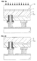
Fig. 3A and Fig. 3B are sectional views illustrating a manner in which the growth substrate is removed from the device structure. -
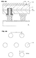
Fig. 4A is a sectional view illustrating a manner in which a photonic crystal layer is provided on a surface of the device structure, andFig. 4B is a plan view illustrating a surface state of the photonic crystal layer. -
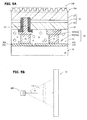
Fig. 5A is a sectional view illustrating a manner in which a wavelength conversion layer is provided between the device structure and a supporting substrate, andFig. 5B is a schematic view illustrating a manner in which light emitted from the device structure is projected onto a screen. - Hereinafter, a description will be given of a method of producing a semiconductor light emitting device (LED device), as well as of operation principles of the semiconductor light emitting device in accordance with embodiment, with reference to
Fig. 1A to Fig. 5B . The manufacturing method of the LED device in accordance with the embodiment includes a step of forming a device structure on a growth substrate (Figs. 1A and 1B ), a step of forming a bonded structure by bonding the device structure to a supporting substrate (Figs. 2A and 2B ), a step of exposing a surface of the device structure by removing the growth substrate from the bonded structure (Figs. 3A and 3B ), a step of providing a photonic crystal layer on a surface of the exposed device structure (Figs. 4A and 4B ), and a step of providing a wavelength conversion layer between the device structure and the supporting substrate (Fig. 5A ). It is to be noted that the relative size and the positional relationship of the components illustrated in drawings are not the same as those of actual products. -
Fig. 1A and Fig. 1B illustrate a manner in which adevice structure 101 is formed on agrowth substrate 11. As thegrowth substrate 11, for example, a C surface sapphire substrate is used. In place of the sapphire surface, for example, a spinel substrate, a ZnO substrate, or the like may be used. - Referring to
Fig. 1A , by using, for example, a MOCVD (metal organic chemical vapor deposition) method, a nitride-based (GaN based) semiconductor layer (optical semiconductor laminate 20) which is expressed by AlxInyGa1-x-yN (0≤x≤1 and 0≤y≤1) is formed on thegrowth substrate 11. First, abase buffer layer 21 made of GaN is formed on thegrowth substrate 11 by using TMG (trimethylgallium) and NH3 as raw material gases. - Then, using TMG, NH3, and SiH4 as the raw material gases, an Si doped GaN layer (n-type GaN layer) is grown on the
base buffer layer 21. The thickness of the n-type GaN layer may be, for example, about5 µm. The n-type GaN layer constitutes an n-type semiconductor layer 22. - Subsequently, a well layer of InGaN is made to grow by using TMI (trimethly indium), TMG, and NH3 as the raw material gases. The thickness of the well layer may be, for example, about 2 nm. Then, a barrier layer of GaN is made to grow by using TMG and NH3 as the raw material gases. The thickness of the barrier layer may be, for example, about 10 nm. Then, growing of the well layer and the barrier layer are cyclically and alternatively repeated (for example, five cycles), whereby an
active layer 23 having a multiple-quantum well structure is formed on the n-type semiconductor layer 22. - After that, an Mg-doped AlGaN layer (p-type AlGaN layer) is made to grow on the
active layer 23, by using TMA (trimethylaluminum), TMG, NH3 and CP2Mg (Biscyclopentadienylmagnesium) as the raw material gas using. The thickness of the p-type AlGaN layer may be, for example, about 15 nm. Next, an Mg-doped GaN layer (p-type GaN layer) is made to grow on the p-type AlGaN layer, by using TMG, NH3 and CP2Mg as the raw material gases. The thickness of the p-type GaN layer may be, for example, about 20 nm. The p-type AlGaN layer and the p-type GaN layer constitute a p-type semiconductor layer 24. - In this way, the
optical semiconductor laminate 20, in which the n-type semiconductor layer 22, theactive layer 23, and the p-type semiconductor layer 24 are sequentially laminated, is formed on thegrowth substrate 11 through the intermediary of thebase buffer layer 21. Theoptical semiconductor laminate 20 thus obtained has, for example, a square planar shape of about 1 mm long and wide. - Next, as illustrated in
Fig. 1B , a via hole (hole) 20d is formed by removing a portion of theoptical semiconductor laminate 20, by a dry etching method employing a resist mask and chlorine gas. The viahole 20d is formed to penetrate at least the p-type semiconductor layer 24 and theactive layer 23, and the n-type semiconductor layer 22 is exposed at the bottom of the via hole. - Then, an n-
side electrode 32, which is connected to the n-type semiconductor layer 22 through the viahole 20d, and a p-side electrode 34, which is connected to the p-type semiconductor layer 24 on a surface of theoptical semiconductor laminate 20, are formed by a lift-off method, for example. As the n-side electrode 32 and the p-side electrode 34, translucent members, such as of ITO (indium tin oxide) or the like are used. - Specifically, a protective insulating layer 32i which covers the inner surface of the via
hole 20d may be formed in advance, in order to avoid electrical short-circuiting between the layers constituting theoptical semiconductor laminate 20 via and along the n-side electrode 32. The protective insulating layer 32i may be made of, for example, SiO2, and may be formed by, for example, a sputtering method, or a dry etching method employing a resist mask and a CF4/Ar gas mixture. - Next, by the lift-off method for example, an n-
side bump 33 and a p-side bump 35 made of Au or the like are respectively formed on the n-side electrode 32 and the p-side electrode 34. Thicknesses (height) of thebumps - In this way, the
device structure 101 is formed on thegrowth substrate 11 to have theoptical semiconductor laminate 20, the n-side electrode 32, the n-side bump 33, the p-side electrode 34, and the p-side bump 35. -
Fig. 2A and Fig. 2B illustrate a manner in which thedevice structure 101 on thegrowth substrate 11 is bonded to a supportingsubstrate 40. Here, thedevice structure 101, which is illustrated inFig. 1B , is illustrated upside down. - First, as illustrated in
Fig. 2A , the supportingsubstrate 40 is prepared. The supportingsubstrate 40 has a configuration in which a lightreflective electrode 42 is provided on a surface of abase material 41. As thebase material 41, for example, an Si substrate may be used. As the lightreflective electrode 42, for example, a member having high light reflectivity and conductivity, such as Ag, Au, or Al, is used. It is to be noted that the lightreflective electrode 42 includes first and second regions (n-side and p-side regions) 42a and 42b which are spaced from each other and not electrically connected to each other. - Subsequently, as illustrated in
Fig. 2B , the supportingsubstrate 40 and thedevice structure 101 are disposed to face each other. Specifically, the first region (n-side region) 42a of the lightreflective electrode 42 is disposed to face the n-side bump 33 of thedevice structure 101, and the second region (p-side region) 42b of the lightreflective electrode 42 is disposed to face the p-side bump 35 of thedevice structure 101. - Next, the supporting
substrate 40 and thedevice structure 101 are brought into contact with each other, and bonded together by, for example, fusion. The resultant structure having the supportingsubstrate 40 and thedevice structure 101 bonded together is referred to as a bondedstructure 102. -
Fig. 3A and Fig. 3B illustrate a manner in which thegrowth substrate 11 is removed from the bondedstructure 102. Thegrowth substrate 11 can be removed by, for example, a laser lift-off method. - As illustrated in
Fig. 3A , KrF excimer laser light is applied to the bonded structure from the same side as the growth substrate 11 (sapphire substrate). The base buffer layer 21 (GaN layer) absorbs the laser light which is transmitted through thegrowth substrate 11. Thebase buffer layer 21 is decomposed by heat generated by absorbed light. Consequently, thegrowth substrate 11 and the optical semiconductor laminate 20 (device structure 101) are separated from each other, and as illustrated inFig. 3B , the n-type semiconductor layer 22 is exposed. -
Fig. 4A illustrates a manner in which aphotonic crystal layer 22p is formed on the exposed surface of the n-type semiconductor layer 22 (device structure 101). A resist mask having a desired pattern is formed on the surface of the n-type semiconductor layer 22 by a nanoimprint method. After that, part of the surface of the n-type semiconductor layer 22 is removed by a drying etching method employing the resist mask and a chlorine gas, thereby formingconcave portions 22h distributed in a two-dimensional cyclic manner. A depth of theconcave portion 22h is, for example, about 360 nm. Moreover, portions which are not removed from and remain in the surface of the n-type semiconductor layer 22 are referred to asconvex portions 22a. -
Fig. 4B illustrates a planar shape and a planar arrangement of theconcave portions 22h. The planar shape of eachconcave portion 22h is, for example, a circle having a diameter D (approximately 200 nm). Theconcave portions 22h are arranged in a triangular lattice shape for example, at a pitch P (approximately 450 nm). - As seen from the above, the
photonic crystal layer 22p includes theconvex portions 22a made of the same material as that of the n-type semiconductor layer 22 and theconcave portions 22h which are filled with atmosphere (air) after selective removal of the n-type semiconductor layer 22. A refractive index of GaN (Si doped) constituting theconvex portions 22a is approximately 2.4, and a refractive index of the air filling theconcave portions 22h is approximately 1.0. Thus, thephotonic crystal layer 22p has a structure in which portions having different refractive indices are arranged in a two-dimensional cyclic manner. -
Fig. 5A illustrates a manner in which the space between theoptical semiconductor laminate 20 and the supportingsubstrate 40 is filled with awavelength conversion layer 50. Thewavelength conversion layer 50 has a structure in whichsemiconductor nanoparticles 52 developing a quantum size effect are dispersed in abinder 51. Thesemiconductor nanoparticles 52 may include various types ofsemiconductor nanoparticles binder 51, for example, silicone resin can be used. In addition, as thesemiconductor nanoparticle 52, for example, InP nanoparticles may be used. - More specifically, as a first step, InP nanoparticles (manufactured by NN-Labs) with light emitting wavelengths of 545 nm and 635 nm are mixed with a commercially available thermosetting silicone resin, by approximately 46 volume %. Next, the silicone resin mixed with the InP nanoparticles is injected to the space between the
optical semiconductor laminate 20 and the supportingsubstrate 40, and then, the silicone resin is thermally cured. Consequently, thewavelength conversion layer 50 is formed provided in the space between theoptical semiconductor laminate 20 and the supportingsubstrate 40. - In this way, an
LED device 100 in accordance with the invention is completed. TheLED device 100 when electrically powered emits white light (blue · green · red light) from thephotonic crystal layer 22p (light emitting surface) at a reduced directivity angle. - Electrical power (current) is supplied to the
optical semiconductor laminate 20, through the n-side region 42a (n-side bump 33 and n-side electrode 32 connected thereto) of the light reflective electrode and the p-side region 42b (p-side bump 35 and p-side electrode 34 connected thereto) of the light reflective electrode. Consequently, electrons which are injected from the n-side electrode 32 to the n-type semiconductor layer 22, and holes which are inserted from the p-side electrode 34 to the p-type semiconductor layer 24, are recombined in theactive layer 23, with the result that energy related to the recombination is radiated as light (and heat). - A part of the light radiated from the
active layer 23 is directly emitted through the surface of the n-type semiconductor layer 22 (photonic crystal layer 22p). Theoptical semiconductor laminate 20 in the described embodiment emits blue light (450 nm wavelength), so that the blue light is emitted from the surface of the n-type semiconductor layer 22 (photonic crystal layer 22p). - Meanwhile, the other part of the light radiated from the
active layer 23 is transmitted through thewavelength conversion layer 50 and reflected by the lightreflective electrode 42, and is then emitted from the surface of the n-type semiconductor layer 22 (photonic crystal layer 22p). Thesemiconductor nanoparticles wavelength conversion layer 50 absorb the light which is radiated from theoptical semiconductor laminate 20, and radiates the light having wavelengths corresponding to the particle diameters. In the example, thesemiconductor nanoparticles optical semiconductor laminate 20, and radiate light beams having 545 nm wavelength and 635 nm wavelength, respectively. That is, thewavelength conversion layer 50 converts the light (blue light) radiated from theoptical semiconductor laminate 20 into green light and red light. Therefore, the surface of the n-type semiconductor layer 22 (photonic crystal layer 22p) emits the green light and the red light. -
Fig. 5B illustrates a manner in which blue, green, and red light, i.e., white light, emitted from theLED device 100, is projected on a screen Sc. Thephotonic crystal layer 22p (refer toFig. 5A ) is provided on the light emitting surface of theLED device 100. - On the screen Sc, the intensity of the light emitted from the
LED device 100 is highest in a forward direction (direction normal to the light emitting surface), and is gradually lowered as the projected light spreads radially outward. A position where light intensity is half the light intensity in the forward direction is illustrated as an inclination angle (directivity angle) θ with respect to the forward direction. The directivity angle θ is generally used as a parameter expressing the directivity of emitted light of a light emitting device. - In a case where the
photonic crystal layer 22p is not provided on the light emitting surface of theLED device 100, that is, a case in which the light emitting surface is constituted by a flat n-type semiconductor layer 22, the directivity angle θ is approximately 60°. In contrast, when thephotonic crystal layer 22p is provided on the light emitting surface of theLED device 100, under the conditions of the embodiment described, the directivity angle θ is approximately 30°. Thus, the directivity angle of the white light emitted from theLED device 100 is decreased by virtue of provision of thephotonic crystal layer 22p. - When the optical semiconductor laminate 20 (device structure) which radiates light of a single wavelength is required to emit light having various wavelengths, such as white light, it is an effective measure to combine the
optical semiconductor laminate 20 with thewavelength conversion layer 50 including the semiconductor nanoparticle. At this time, when thewavelength conversion layer 50 is provided on the same side of theoptical semiconductor laminate 20 as thephotonic crystal layer 22p (light emitting surface side), the effect of thephotonic crystal layer 22p to decrease the directivity angle of the emitted light is reduced. For this reason, as illustrated inFig. 5A , thewavelength conversion layer 50 is desired to be provided on an opposite side of thephotonic crystal layer 22p (light emitting surface) with respect to theoptical semiconductor laminate 20. - It is also to be understood that, when total refractive index of the
wavelength conversion layer 50 is smaller than the refractive index of the optical semiconductor laminate 20 (particularly, p-type semiconductor layer 24), the light radiated from theoptical semiconductor laminate 20 is reflected from a boundary between the optical semiconductor laminate and thewavelength conversion layer 50, failing to be incident to thewavelength conversion layer 50. Therefore, the total refractive index of thewavelength conversion layer 50 is desired to be equal to or greater than the refractive index of theoptical semiconductor laminate 20. - In the described embodiment, the
optical semiconductor laminate 20 is constituted by a GaN based semiconductor (refractive index of approximately 2.4), while thewavelength conversion layer 50 is constituted by the binder 51 (refractive index of 1.4 to 1.5) and thesemiconductor nanoparticles 52 of InP (refractive index of approximately 3.5). In this case, a volume ratio of the semiconductor nanoparticles with respective to the binder is preferably not less than 46%, in order to obtain a refractive index of the wavelength conversion layer not smaller than the refractive index of the optical semiconductor laminate. - In addition, in a case where the
optical semiconductor laminate 20 is constituted by the GaN based semiconductor, a material having a refractive index which is at least greater than the refractive index of the GaN based semiconductor is preferably used, as the material of thesemiconductor nanoparticle 52 included in thewavelength conversion layer 50. For example, the material of thesemiconductor nanoparticle 52 is at least one selected from the group consisting of AgInS2, CuInS2, ZnSe, ZnTe, CdS, CdSe, CdTe, AlN, GaN, InN, InP, AlGaN, AlInN, and GaInN. - Although the invention has been described in terms of a specific embodiment, the invention is not limited to the described embodiment. For instance, although an LED device of a via hole electrode type (flip-chip type) has been described, the LED device may be of a surface electrode type, or the like. Any type of electrode structure may be employed provided that it allows electrical power supply to an optical semiconductor laminate. In addition, as a two-dimensional cyclic structure of the photonic crystal layer, any structure (shape and arrangement pattern of concave portion) may be used as long as it serves to decrease the directivity angle of the emitted light. A structure which increases the directivity angle of the emitted light may also be employed, depending on the use of the LED device. Other changes, modifications and combinations will be obvious to those skilled in the art.
- All examples and conditional language recited herein are intended for pedagogical purposes to aid the reader in understanding the invention and the concepts contributed by the inventors to furthering the art, and are to be construed as being without limitation to such specifically recited examples and conditions, nor does the organization of such examples in the specification relate to a showing of the superiority and inferiority of the invention. Although the embodiments of the invention have been described in detail, it should be understood that the various changes, substitutions, and alterations could be made hereto without departing from the spirit and scope of the invention.
Claims (5)
- A semiconductor light emitting device, comprising:a supporting substrate that has light reflecting characteristics;a wavelength conversion layer that is disposed on the supporting substrate, and contains semiconductor nanoparticles developing a quantum size effect;an optical semiconductor laminate that is disposed on the wavelength conversion layer and has light emitting characteristics; anda photonic crystal layer that is disposed on the optical semiconductor laminate, and that has first portions having a first refractive index and second portions having a second refractive index different from the first refractive index, the first portions and the second portions being arranged in a two-dimensional cyclic pattern.
- The semiconductor light emitting device according to claim 1, wherein the refractive index of the semiconductor nanoparticles is greater than the refractive index of the optical semiconductor laminate.
- The semiconductor light emitting device according to claim 2, wherein a total refractive index of the wavelength conversion layer is equal to or greater than the refractive index of the optical semiconductor laminate.
- The semiconductor light emitting device according to claim 1,
wherein the optical semiconductor laminate includes a GaN based semiconductor, and
wherein the semiconductor nanoparticles are made of at least one material selected from the group consisting of AgInS2, CuInS2, ZnSe, ZnTe, CdS, CdSe, CdTe, AlN, GaN, InN, InP, AlGaN, AlInN, and GaInN. - The semiconductor light emitting device according to claim 1,
wherein the optical semiconductor laminate has a structure in which a p-type semiconductor layer, an active layer having light emitting characteristics, and an n-type semiconductor layer are stacked in order from the wavelength conversion layer side, and
wherein, the first portions of the photonic crystal layer are made of the material constituting the n-type semiconductor layer, and the second portions of the photonic crystal layer are constituted by air.
Applications Claiming Priority (1)
| Application Number | Priority Date | Filing Date | Title |
|---|---|---|---|
| JP2015008286A JP2016134501A (en) | 2015-01-20 | 2015-01-20 | Semiconductor light emitting device |
Publications (1)
| Publication Number | Publication Date |
|---|---|
| EP3048651A1 true EP3048651A1 (en) | 2016-07-27 |
Family
ID=55085607
Family Applications (1)
| Application Number | Title | Priority Date | Filing Date |
|---|---|---|---|
| EP16151088.8A Withdrawn EP3048651A1 (en) | 2015-01-20 | 2016-01-13 | Semiconductor light emitting device |
Country Status (3)
| Country | Link |
|---|---|
| US (1) | US9634200B2 (en) |
| EP (1) | EP3048651A1 (en) |
| JP (1) | JP2016134501A (en) |
Families Citing this family (8)
| Publication number | Priority date | Publication date | Assignee | Title |
|---|---|---|---|---|
| US10269776B2 (en) * | 2014-12-16 | 2019-04-23 | PlayNitride Inc. | Light emitting device |
| US20190296188A1 (en) * | 2017-01-10 | 2019-09-26 | PlayNitride Display Co., Ltd. | Micro light-emitting diode chip |
| US12015103B2 (en) * | 2017-01-10 | 2024-06-18 | PlayNitride Display Co., Ltd. | Micro light emitting diode display panel with option of choosing to emit light both or respectively of light-emitting regions |
| WO2018170531A1 (en) * | 2017-03-21 | 2018-09-27 | Newsouth Innovations Pty Ltd | A light emitting device |
| US10991856B2 (en) | 2017-12-21 | 2021-04-27 | Lumileds Llc | LED with structured layers and nanophosphors |
| WO2020040132A1 (en) * | 2018-08-23 | 2020-02-27 | 株式会社ニコン | Light emission device, light emission method, exposure device and device manufacturing method |
| CN109285928B (en) * | 2018-09-28 | 2020-08-25 | 厦门乾照光电股份有限公司 | Flip LED chip and manufacturing method thereof |
| KR102900223B1 (en) * | 2020-09-29 | 2025-12-16 | 삼성전자주식회사 | Micro led and display module having the same |
Citations (6)
| Publication number | Priority date | Publication date | Assignee | Title |
|---|---|---|---|---|
| JP2006059864A (en) | 2004-08-17 | 2006-03-02 | Yokohama National Univ | Light emitting element |
| EP1909335A1 (en) * | 2005-06-09 | 2008-04-09 | Rohm Co., Ltd. | Semiconductor light emitting element |
| WO2010075599A1 (en) * | 2008-12-16 | 2010-07-08 | D. Swarovski & Co. | Transparent body with invisible led light source |
| JP2013149729A (en) * | 2012-01-18 | 2013-08-01 | Fujifilm Corp | Quantum dot structure, wavelength conversion element, and photoelectric conversion device |
| US20150008393A1 (en) * | 2013-07-03 | 2015-01-08 | Benjamin Daniel Mangum | Network of semiconductor structures with fused insulator coating |
| US20150014720A1 (en) * | 2013-07-10 | 2015-01-15 | Lextar Electronics Corporation | Light emitting diode package structure |
Family Cites Families (7)
| Publication number | Priority date | Publication date | Assignee | Title |
|---|---|---|---|---|
| US6366018B1 (en) | 1998-10-21 | 2002-04-02 | Sarnoff Corporation | Apparatus for performing wavelength-conversion using phosphors with light emitting diodes |
| JP4587675B2 (en) * | 2004-01-23 | 2010-11-24 | 京セラ株式会社 | Light emitting element storage package and light emitting device |
| JP4976849B2 (en) * | 2004-07-12 | 2012-07-18 | ローム株式会社 | Semiconductor light emitting device |
| US7745843B2 (en) * | 2006-09-26 | 2010-06-29 | Stanley Electric Co., Ltd. | Semiconductor light emitting device |
| US20110182056A1 (en) * | 2010-06-23 | 2011-07-28 | Soraa, Inc. | Quantum Dot Wavelength Conversion for Optical Devices Using Nonpolar or Semipolar Gallium Containing Materials |
| JP5622494B2 (en) * | 2010-09-09 | 2014-11-12 | スタンレー電気株式会社 | Light emitting device and manufacturing method thereof |
| JP6062431B2 (en) * | 2012-06-18 | 2017-01-18 | シャープ株式会社 | Semiconductor light emitting device |
-
2015
- 2015-01-20 JP JP2015008286A patent/JP2016134501A/en active Pending
-
2016
- 2016-01-07 US US14/990,433 patent/US9634200B2/en active Active
- 2016-01-13 EP EP16151088.8A patent/EP3048651A1/en not_active Withdrawn
Patent Citations (6)
| Publication number | Priority date | Publication date | Assignee | Title |
|---|---|---|---|---|
| JP2006059864A (en) | 2004-08-17 | 2006-03-02 | Yokohama National Univ | Light emitting element |
| EP1909335A1 (en) * | 2005-06-09 | 2008-04-09 | Rohm Co., Ltd. | Semiconductor light emitting element |
| WO2010075599A1 (en) * | 2008-12-16 | 2010-07-08 | D. Swarovski & Co. | Transparent body with invisible led light source |
| JP2013149729A (en) * | 2012-01-18 | 2013-08-01 | Fujifilm Corp | Quantum dot structure, wavelength conversion element, and photoelectric conversion device |
| US20150008393A1 (en) * | 2013-07-03 | 2015-01-08 | Benjamin Daniel Mangum | Network of semiconductor structures with fused insulator coating |
| US20150014720A1 (en) * | 2013-07-10 | 2015-01-15 | Lextar Electronics Corporation | Light emitting diode package structure |
Also Published As
| Publication number | Publication date |
|---|---|
| US9634200B2 (en) | 2017-04-25 |
| JP2016134501A (en) | 2016-07-25 |
| US20160211422A1 (en) | 2016-07-21 |
Similar Documents
| Publication | Publication Date | Title |
|---|---|---|
| US9634200B2 (en) | Semiconductor light emitting device | |
| JP4992282B2 (en) | Light emitting diode, light emitting diode manufacturing method, light emitting diode backlight, light emitting diode illumination device, light emitting diode display, and electronic device | |
| JP6947386B2 (en) | Semiconductor light emitting element and manufacturing method of semiconductor light emitting element | |
| US8269238B2 (en) | Photonic crystal light emitting device using photon-recycling | |
| CN205508818U (en) | Lighting device | |
| TWI630733B (en) | Light-emitting element package and method of manufacturing same | |
| JP6934812B2 (en) | Light emitting element and light emitting element array including it | |
| JP6852066B2 (en) | Wavelength conversion type light emitting device with a texture substrate | |
| US9136448B2 (en) | Semiconductor light emitting device lamp that emits light at large angles | |
| TWI607612B (en) | Semiconductor laser device | |
| JP2002222989A (en) | Semiconductor light emitting device | |
| JP2014160736A (en) | Semiconductor light emitting device and light emitting device | |
| US9178124B2 (en) | Light emitting device and light emitting device package | |
| KR102227774B1 (en) | Method for manufacturing light emitting diode package | |
| CN107210338A (en) | Light emitting diode | |
| WO2011030789A1 (en) | Light-emitting device | |
| JP2010135746A (en) | Semiconductor light-emitting element and method of manufacturing the same, light-emitting device | |
| US9680063B2 (en) | Semiconductor light-emitting device and semiconductor light-emitting device array | |
| CN114649452A (en) | Lighting fixtures and projectors | |
| CN103460414B (en) | Semiconductor chip, the display with multiple semiconductor chip and its manufacture method | |
| JP2013098571A (en) | Semiconductor light-emitting element and manufacturing method of the same | |
| JP6829562B2 (en) | Vertical resonator type light emitting element laser module | |
| KR102077232B1 (en) | Lighting device | |
| JP2026508889A (en) | Surface-emitting laser, method for manufacturing a surface-emitting laser | |
| JP2014225588A (en) | Semiconductor light-emitting element array |
Legal Events
| Date | Code | Title | Description |
|---|---|---|---|
| PUAI | Public reference made under article 153(3) epc to a published international application that has entered the european phase |
Free format text: ORIGINAL CODE: 0009012 |
|
| AK | Designated contracting states |
Kind code of ref document: A1 Designated state(s): AL AT BE BG CH CY CZ DE DK EE ES FI FR GB GR HR HU IE IS IT LI LT LU LV MC MK MT NL NO PL PT RO RS SE SI SK SM TR |
|
| AX | Request for extension of the european patent |
Extension state: BA ME |
|
| STAA | Information on the status of an ep patent application or granted ep patent |
Free format text: STATUS: THE APPLICATION IS DEEMED TO BE WITHDRAWN |
|
| 18D | Application deemed to be withdrawn |
Effective date: 20170128 |